JP6587599B2 - Object detection device - Google Patents
Object detection device Download PDFInfo
- Publication number
- JP6587599B2 JP6587599B2 JP2016235466A JP2016235466A JP6587599B2 JP 6587599 B2 JP6587599 B2 JP 6587599B2 JP 2016235466 A JP2016235466 A JP 2016235466A JP 2016235466 A JP2016235466 A JP 2016235466A JP 6587599 B2 JP6587599 B2 JP 6587599B2
- Authority
- JP
- Japan
- Prior art keywords
- substrate
- light
- object detection
- mounting surface
- light receiving
- Prior art date
- Legal status (The legal status is an assumption and is not a legal conclusion. Google has not performed a legal analysis and makes no representation as to the accuracy of the status listed.)
- Expired - Fee Related
Links
Images


Classifications
-
- G—PHYSICS
- G01—MEASURING; TESTING
- G01S—RADIO DIRECTION-FINDING; RADIO NAVIGATION; DETERMINING DISTANCE OR VELOCITY BY USE OF RADIO WAVES; LOCATING OR PRESENCE-DETECTING BY USE OF THE REFLECTION OR RERADIATION OF RADIO WAVES; ANALOGOUS ARRANGEMENTS USING OTHER WAVES
- G01S17/00—Systems using the reflection or reradiation of electromagnetic waves other than radio waves, e.g. lidar systems
- G01S17/02—Systems using the reflection of electromagnetic waves other than radio waves
- G01S17/06—Systems determining position data of a target
- G01S17/08—Systems determining position data of a target for measuring distance only
-
- G—PHYSICS
- G01—MEASURING; TESTING
- G01B—MEASURING LENGTH, THICKNESS OR SIMILAR LINEAR DIMENSIONS; MEASURING ANGLES; MEASURING AREAS; MEASURING IRREGULARITIES OF SURFACES OR CONTOURS
- G01B11/00—Measuring arrangements characterised by the use of optical techniques
- G01B11/02—Measuring arrangements characterised by the use of optical techniques for measuring length, width or thickness
- G01B11/026—Measuring arrangements characterised by the use of optical techniques for measuring length, width or thickness by measuring distance between sensor and object
-
- G—PHYSICS
- G01—MEASURING; TESTING
- G01B—MEASURING LENGTH, THICKNESS OR SIMILAR LINEAR DIMENSIONS; MEASURING ANGLES; MEASURING AREAS; MEASURING IRREGULARITIES OF SURFACES OR CONTOURS
- G01B11/00—Measuring arrangements characterised by the use of optical techniques
- G01B11/14—Measuring arrangements characterised by the use of optical techniques for measuring distance or clearance between spaced objects or spaced apertures
-
- G—PHYSICS
- G01—MEASURING; TESTING
- G01C—MEASURING DISTANCES, LEVELS OR BEARINGS; SURVEYING; NAVIGATION; GYROSCOPIC INSTRUMENTS; PHOTOGRAMMETRY OR VIDEOGRAMMETRY
- G01C3/00—Measuring distances in line of sight; Optical rangefinders
- G01C3/02—Details
- G01C3/06—Use of electric means to obtain final indication
- G01C3/08—Use of electric radiation detectors
-
- G—PHYSICS
- G01—MEASURING; TESTING
- G01S—RADIO DIRECTION-FINDING; RADIO NAVIGATION; DETERMINING DISTANCE OR VELOCITY BY USE OF RADIO WAVES; LOCATING OR PRESENCE-DETECTING BY USE OF THE REFLECTION OR RERADIATION OF RADIO WAVES; ANALOGOUS ARRANGEMENTS USING OTHER WAVES
- G01S17/00—Systems using the reflection or reradiation of electromagnetic waves other than radio waves, e.g. lidar systems
- G01S17/02—Systems using the reflection of electromagnetic waves other than radio waves
- G01S17/04—Systems determining the presence of a target
-
- G—PHYSICS
- G01—MEASURING; TESTING
- G01S—RADIO DIRECTION-FINDING; RADIO NAVIGATION; DETERMINING DISTANCE OR VELOCITY BY USE OF RADIO WAVES; LOCATING OR PRESENCE-DETECTING BY USE OF THE REFLECTION OR RERADIATION OF RADIO WAVES; ANALOGOUS ARRANGEMENTS USING OTHER WAVES
- G01S17/00—Systems using the reflection or reradiation of electromagnetic waves other than radio waves, e.g. lidar systems
- G01S17/02—Systems using the reflection of electromagnetic waves other than radio waves
- G01S17/06—Systems determining position data of a target
- G01S17/42—Simultaneous measurement of distance and other co-ordinates
-
- G—PHYSICS
- G01—MEASURING; TESTING
- G01S—RADIO DIRECTION-FINDING; RADIO NAVIGATION; DETERMINING DISTANCE OR VELOCITY BY USE OF RADIO WAVES; LOCATING OR PRESENCE-DETECTING BY USE OF THE REFLECTION OR RERADIATION OF RADIO WAVES; ANALOGOUS ARRANGEMENTS USING OTHER WAVES
- G01S17/00—Systems using the reflection or reradiation of electromagnetic waves other than radio waves, e.g. lidar systems
- G01S17/88—Lidar systems specially adapted for specific applications
-
- G—PHYSICS
- G01—MEASURING; TESTING
- G01S—RADIO DIRECTION-FINDING; RADIO NAVIGATION; DETERMINING DISTANCE OR VELOCITY BY USE OF RADIO WAVES; LOCATING OR PRESENCE-DETECTING BY USE OF THE REFLECTION OR RERADIATION OF RADIO WAVES; ANALOGOUS ARRANGEMENTS USING OTHER WAVES
- G01S7/00—Details of systems according to groups G01S13/00, G01S15/00, G01S17/00
- G01S7/48—Details of systems according to groups G01S13/00, G01S15/00, G01S17/00 of systems according to group G01S17/00
- G01S7/481—Constructional features, e.g. arrangements of optical elements
- G01S7/4811—Constructional features, e.g. arrangements of optical elements common to transmitter and receiver
- G01S7/4812—Constructional features, e.g. arrangements of optical elements common to transmitter and receiver transmitted and received beams following a coaxial path
-
- G—PHYSICS
- G01—MEASURING; TESTING
- G01S—RADIO DIRECTION-FINDING; RADIO NAVIGATION; DETERMINING DISTANCE OR VELOCITY BY USE OF RADIO WAVES; LOCATING OR PRESENCE-DETECTING BY USE OF THE REFLECTION OR RERADIATION OF RADIO WAVES; ANALOGOUS ARRANGEMENTS USING OTHER WAVES
- G01S7/00—Details of systems according to groups G01S13/00, G01S15/00, G01S17/00
- G01S7/48—Details of systems according to groups G01S13/00, G01S15/00, G01S17/00 of systems according to group G01S17/00
- G01S7/481—Constructional features, e.g. arrangements of optical elements
- G01S7/4811—Constructional features, e.g. arrangements of optical elements common to transmitter and receiver
- G01S7/4813—Housing arrangements
-
- G—PHYSICS
- G01—MEASURING; TESTING
- G01S—RADIO DIRECTION-FINDING; RADIO NAVIGATION; DETERMINING DISTANCE OR VELOCITY BY USE OF RADIO WAVES; LOCATING OR PRESENCE-DETECTING BY USE OF THE REFLECTION OR RERADIATION OF RADIO WAVES; ANALOGOUS ARRANGEMENTS USING OTHER WAVES
- G01S7/00—Details of systems according to groups G01S13/00, G01S15/00, G01S17/00
- G01S7/48—Details of systems according to groups G01S13/00, G01S15/00, G01S17/00 of systems according to group G01S17/00
- G01S7/481—Constructional features, e.g. arrangements of optical elements
- G01S7/4817—Constructional features, e.g. arrangements of optical elements relating to scanning
-
- G—PHYSICS
- G01—MEASURING; TESTING
- G01V—GEOPHYSICS; GRAVITATIONAL MEASUREMENTS; DETECTING MASSES OR OBJECTS; TAGS
- G01V8/00—Prospecting or detecting by optical means
- G01V8/10—Detecting, e.g. by using light barriers
-
- G—PHYSICS
- G01—MEASURING; TESTING
- G01V—GEOPHYSICS; GRAVITATIONAL MEASUREMENTS; DETECTING MASSES OR OBJECTS; TAGS
- G01V8/00—Prospecting or detecting by optical means
- G01V8/10—Detecting, e.g. by using light barriers
- G01V8/12—Detecting, e.g. by using light barriers using one transmitter and one receiver
Landscapes
- Physics & Mathematics (AREA)
- Engineering & Computer Science (AREA)
- General Physics & Mathematics (AREA)
- Radar, Positioning & Navigation (AREA)
- Remote Sensing (AREA)
- Computer Networks & Wireless Communication (AREA)
- Electromagnetism (AREA)
- Life Sciences & Earth Sciences (AREA)
- General Life Sciences & Earth Sciences (AREA)
- Geophysics (AREA)
- Optical Radar Systems And Details Thereof (AREA)
- Geophysics And Detection Of Objects (AREA)
- Mechanical Optical Scanning Systems (AREA)
Description
本発明は、発光素子から光を投射し、その反射光を受光素子で受光した結果に基づいて対象物を検出する物体検出装置に関する。 The present invention relates to an object detection apparatus that detects an object based on a result of projecting light from a light emitting element and receiving the reflected light by a light receiving element.
たとえば、車載用のレーザレーダのような物体検出装置は、発光素子から光を投光し、その反射光を受光素子で受光した結果に基づいて対象物の有無を検出する。また、発光素子から光を投光して、対象物からの反射光を受光素子で受光するまでの時間に基づいて、対象物までの距離を検出する物体検出装置もある。 For example, an object detection device such as a vehicle-mounted laser radar projects light from a light emitting element and detects the presence or absence of an object based on the result of receiving the reflected light by a light receiving element. There is also an object detection device that detects a distance to an object based on a time from when light is emitted from a light emitting element until reflected light from the object is received by a light receiving element.
発光素子としてはレーザダイオードなどが用いられ、受光素子としてはフォトダイオードなどが用いられる。たとえば特許文献1〜8のように、発光素子から投射された光は、投光レンズや鏡などの投光系の光学部品を経て、光偏向器により偏向されて対象物に照射される。そして、対象物で反射された光は、光偏向器により偏向された後、鏡や受光レンズなどの受光系の光学部品を経て、受光素子で受光される。なお、特許文献1では、対象物からの反射光が、光偏向器を経ずに、受光レンズで集光されて、受光素子で受光される。光偏向器は、たとえば回転鏡から成る。
A laser diode or the like is used as the light emitting element, and a photodiode or the like is used as the light receiving element. For example, as disclosed in
対象物に対して光を投受光するために、特許文献1、特許文献2、特許文献4、および特許文献8では、発光素子と受光素子とが別々の基板に実装されている。特許文献5では、発光素子と受光素子とが同一の板状部材(符号1a)に実装されている。そして、これらの特許文献のいずれにおいても、発光素子は、基板の実装面に対して主に垂直な方向に光を投射するように、該実装面に実装されている。受光素子は、基板の実装面に対して主に垂直な方向から来る光を受光するように、該実装面に実装されている。
In
また、特許文献1では、発光素子を実装した基板と、受光素子を実装した基板とが、同一平面上に平行に配置されている。特許文献2および特許文献8では、発光素子を実装した基板と、受光素子を実装した基板とが、垂直に配置されている。
Moreover, in
発光素子と受光素子とを別々の基板に実装した場合、一方の基板と他方の基板とを、同一平面上に板面が位置するように並べて配置すると、該並び方向に装置が大型化してしまう。一方、2つの基板を両方の板面が垂直になるように位置決めすることは、両方の板面が平行になるように位置決めすることに比べて困難である。 When the light emitting element and the light receiving element are mounted on separate substrates, if one substrate and the other substrate are arranged side by side so that the plate surfaces are positioned on the same plane, the apparatus becomes large in the arrangement direction. . On the other hand, positioning the two substrates so that both plate surfaces are vertical is more difficult than positioning them so that both plate surfaces are parallel.
本発明は、発光素子と受光素子とを別々の基板に実装した物体検出装置において、基板同士を容易に位置決めするとともに、装置を小型化することを課題とする。 An object of the present invention is to easily position the substrates in an object detection apparatus in which a light emitting element and a light receiving element are mounted on separate substrates, and downsize the apparatus.
本発明による物体検出装置は、発光素子と、発光素子を実装した第1基板と、受光素子と、受光素子を実装した第2基板と、第1基板と第2基板とを保持する保持部材と、発光素子から投射された投射光を偏向して対象物に照射し、対象物で反射された反射光を偏向する光偏向器と、光偏向器で偏向された反射光を反射して受光素子に導く反射鏡とを備える。発光素子は、第1基板の実装面に対して主に平行な方向に光を投射するように、第1基板の実装面に実装されている。受光素子は、第2基板の実装面に対して主に垂直な方向に向かって来る光を受光するように、第2基板の実装面に実装されている。保持部材は、第1基板の実装面に対して垂直な投影面と、第2基板の実装面に対して垂直な投影面とが重なるように、第1基板と第2基板とを平行に保持する。 An object detection apparatus according to the present invention includes a light emitting element, a first substrate on which the light emitting element is mounted, a light receiving element, a second substrate on which the light receiving element is mounted, and a holding member that holds the first substrate and the second substrate. , An optical deflector for deflecting the projection light projected from the light emitting element to irradiate the object and deflecting the reflected light reflected by the object, and a light receiving element for reflecting the reflected light deflected by the optical deflector And a reflecting mirror that leads to The light emitting element is mounted on the mounting surface of the first substrate so as to project light in a direction mainly parallel to the mounting surface of the first substrate. The light receiving element is mounted on the mounting surface of the second substrate so as to receive light mainly coming in a direction perpendicular to the mounting surface of the second substrate. The holding member holds the first substrate and the second substrate in parallel such that a projection surface perpendicular to the mounting surface of the first substrate and a projection surface perpendicular to the mounting surface of the second substrate overlap. To do.
上記によると、第1基板に実装された発光素子から、第1基板の実装面に対して主に平行な方向に光が投射され、該投射光が光偏向器により偏向されて、対象物に照射される。そして、対象物で反射された反射光が、光偏向器により偏向された後、反射鏡により第2基板に対して垂直な方向に反射され、第2基板に実装された受光素子により受光される。このため、発光素子から第1基板の実装面に対して平行に光を投射しても、光の偏向により、対象物で反射した光を受光素子で受光して物体を検出することができる。また、本発明では、発光素子による主な光の投光方向と、受光素子による主な光の受光方向とが垂直になるように、発光素子と受光素子とを配置している。そして、そのために、発光素子を実装した第1基板と受光素子を実装した第2基板とを、両方の実装面すなわち板面が平行になるように、保持部材により保持している。このため、第1基板と第2基板の板面が垂直になるように位置決めする場合に比べて、第1基板と第2基板とを容易に位置決めすることができる。さらに、各基板の実装面に対して垂直な投影面が重なるように、第1基板と第2基板とを配置している。このため、各基板を同一平面上に板面が位置するように並べて配置する場合に比べて、投影面が重なった分だけ、物体検出装置を小型化することができる。 According to the above, light is projected from the light emitting element mounted on the first substrate in a direction mainly parallel to the mounting surface of the first substrate, and the projection light is deflected by the optical deflector to be applied to the object. Irradiated. The reflected light reflected by the object is deflected by the optical deflector, then reflected by the reflecting mirror in the direction perpendicular to the second substrate, and received by the light receiving element mounted on the second substrate. . For this reason, even if light is projected in parallel from the light emitting element to the mounting surface of the first substrate, the light reflected by the object can be received by the light receiving element and the object can be detected by the deflection of the light. In the present invention, the light emitting element and the light receiving element are arranged so that the main light projecting direction by the light emitting element is perpendicular to the main light receiving direction by the light receiving element. For this purpose, the first substrate on which the light emitting element is mounted and the second substrate on which the light receiving element is mounted are held by the holding member so that both mounting surfaces, that is, the plate surfaces are parallel to each other. For this reason, compared with the case where it positions so that the board surface of a 1st board | substrate and a 2nd board | substrate may become perpendicular | vertical, a 1st board | substrate and a 2nd board | substrate can be positioned easily. Furthermore, the first substrate and the second substrate are arranged so that the projection surfaces perpendicular to the mounting surfaces of the respective substrates overlap. For this reason, compared with the case where each board | substrate is arrange | positioned side by side so that a plate surface may be located on the same plane, an object detection apparatus can be reduced in size by the part which the projection surface overlapped.
本発明において、保持部材は、第1基板を第2基板に対して対象物側に保持してもよい。 In the present invention, the holding member may hold the first substrate on the object side with respect to the second substrate.
また、本発明において、光偏向器と反射鏡とは、第2基板に対して対象物側に配置され、光偏向器は、発光素子からの投射光を第1基板の対象物側に偏向し、対象物からの反射光を主に両基板と平行な方向へ偏向し、反射鏡は、光偏向器で偏向された反射光を第2基板に対して垂直な方向に反射してもよい。 In the present invention, the light deflector and the reflecting mirror are disposed on the object side with respect to the second substrate, and the light deflector deflects the projection light from the light emitting element toward the object side of the first substrate. The reflected light from the object may be deflected mainly in a direction parallel to the two substrates, and the reflecting mirror may reflect the reflected light deflected by the optical deflector in a direction perpendicular to the second substrate.
また、本発明において、保持部材は反射鏡も保持してもよい。 In the present invention, the holding member may also hold a reflecting mirror.
また、本発明において、発光素子と受光素子と光偏向器の動作を制御し、受光素子から出力される受光信号に基づいて対象物を検出する制御部をさらに備え、制御部は第2基板に実装されていてもよい。 The present invention further includes a control unit that controls operations of the light emitting element, the light receiving element, and the optical deflector, and detects an object based on a light reception signal output from the light receiving element. The control unit is provided on the second substrate. May be implemented.
さらに、本発明において、第1基板は、第2基板より面積が小さく、第2基板の実装面に対して垂直な投影面内に、第1基板の実装面に対して垂直な投影面が収まるように、第1基板と第2基板とが配置されてもよい。 Furthermore, in the present invention, the first substrate has a smaller area than the second substrate, and the projection plane perpendicular to the mounting surface of the first substrate is within the projection surface perpendicular to the mounting surface of the second substrate. As described above, the first substrate and the second substrate may be disposed.
本発明によれば、発光素子と受光素子とを別々の基板に実装した物体検出装置において、基板同士を容易に位置決めすることができ、かつ装置を小型化することが可能となる。 According to the present invention, in an object detection device in which a light emitting element and a light receiving element are mounted on separate substrates, the substrates can be easily positioned with each other, and the device can be miniaturized.
以下、本発明の実施形態につき、図面を参照しながら説明する。各図において、同一の部分または対応する部分には、同一符号を付してある。 Hereinafter, embodiments of the present invention will be described with reference to the drawings. In the drawings, the same or corresponding parts are denoted by the same reference numerals.
まず、実施形態の物体検出装置100の電気的構成を、図1を参照しながら説明する。
First, an electrical configuration of the
図1は、物体検出装置100の電気的構成図である。物体検出装置100は、車載用のレーザレーダである。制御部1は、CPUなどから成り、物体検出装置100の各部の動作を制御する。
FIG. 1 is an electrical configuration diagram of the
LD(レーザダイオード)モジュール2はパッケージ化されている。LDモジュール2には、光源であるLD(レーザダイオード)が複数(たとえば4チャンネル)含まれている。各LDは、高出力光パルスを発する発光素子である。充電回路3は、LDモジュール2と接続されている。
The LD (laser diode)
制御部1は、LDモジュール2の各LDの動作を制御する。詳しくは、たとえば制御部1は、各LDを発光させて、人や物体などの対象物に光を投射する。また、制御部1は、各LDの発光を停止させて、充電回路3により各LDを充電する。
The
モータ4cは、後述する光偏向器4(図3など)の駆動源である。モータ駆動回路5は、モータ4cを駆動させる。エンコーダ6は、モータ4cの回転状態(角度や回転数など)を検出する。制御部1は、モータ駆動回路5によりモータ4cを回転させて、光偏向器4の動作を制御する。また、制御部1は、エンコーダ6の出力に基づいて、光偏向器4の動作状態(動作量や動作位置など)を検出する。
The
PD(フォトダイオード)モジュール7はパッケージ化されている。PDモジュール7には、受光素子であるPD、TIA(トランスインピーダンスアンプ)、MUX(マルチプレクサ)、およびVGA(可変ゲインアンプ)が含まれている(詳細回路は図示省略)。
The PD (photodiode)
PDは、PDモジュール7に複数(たとえば32チャンネル)設けられている。MUXは、TIAの出力信号をVGAに入力させる。昇圧回路9は、フォトダイオードの動作に必要な昇圧された電圧を、PDモジュール7の各PDに供給する。ADC(アナログデジタルコンバータ)8は、PDモジュール7から出力されるアナログ信号を、デジタル信号に変換する。
A plurality of PDs (for example, 32 channels) are provided in the
制御部1は、PDモジュール7の各部の動作を制御する。詳しくは、たとえば制御部1は、LDモジュール2のLDを発光させることにより、対象物で反射された光をPDモジュール7のPDにより受光する。そして、制御部1は、その受光状態に応じてPDから出力される受光信号を、PDモジュール7のTIAおよびVGAにより信号処理する。さらに、制御部1は、PDモジュール7から出力されるアナログの受光信号を、ADC8によりデジタルの受光信号に変換し、該デジタルの受光信号に基づいて、対象物の有無を検出する。また、制御部1は、LDが光を発してから対象物での反射光をPDで受光するまでの時間を算出し、該時間に基づいて対象物までの距離を検出する。
The
記憶部10は、揮発性や不揮発性のメモリから成る。記憶部10には、制御部1が物体検出装置100の各部を制御するための情報や、対象物を検出するための情報などが記憶されている。インタフェイス11は、イーサネット(登録商標)などの通信回路から成る。制御部1は、車両に搭載されたECU(電子制御装置)に対して、インタフェイス11により対象物に関する情報を送受信したり、各種制御情報を送受信したりする。
The
次に、物体検出装置100の構造および機能について、図2〜図10を参照しながら説明する。
Next, the structure and function of the
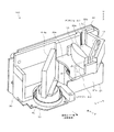
図2は、物体検出装置100の外観を示した斜視図である。図3〜図9は、物体検出装置100の内部構造を示した図である。詳しくは、図3は、物体検出装置100の内部構造を示した斜視図である。図4は、図3から保持部材30を省略した状態を示した図である。図5は、物体検出装置100の内部構造を示した正面図である。図6は、物体検出装置100の内部構造を示した平面図である。図7は、図6から保持部材30を省略した状態を示した図である。図8は、物体検出装置100の内部構造を示した側面図である。図9は、図8から保持部材30を省略した状態を示した図である。
FIG. 2 is a perspective view showing the appearance of the
図2に示すように、物体検出装置100のケース12は、正面視が矩形状の箱体である。ケース12の開口部12aは、透光カバー13で覆われている。透光カバー13は、所定の厚みのドーム状に形成されている。
As shown in FIG. 2, the
ケース12と透光カバー13で囲まれた内部空間には、図3〜図9に示すような光学系と、図1に示した電気系などが収納されている。図2の透光カバー13は、ケース12の内外に対して光を透過させる。
In the internal space surrounded by the
物体検出装置100は、たとえば、透光カバー13が車両の前方、後方、または左右側方を向くように、車両の前部、後部、または左右側部に設置される。その際、図2に示すように、ケース12の短辺方向が上下方向U、Dを向くように、物体検出装置100は車両に設置される。
The
図3〜図9に示すように、ケース12などの内部空間に収納された光学系は、LDモジュール2のLD、投光レンズ14、光偏向器4、受光レンズ16、反射鏡17、およびPDモジュール7のPDから成る。
As shown in FIGS. 3 to 9, the optical system housed in the internal space such as the
そのうち、LDモジュール2のLD、投光レンズ14、および光偏向器4は、投射光学系である。また、光偏向器4、受光レンズ16、反射鏡17、およびPDモジュール7のPDは、受光光学系である。
Among them, the LD of the
図4などに示すように、LDモジュール2は、厚みの薄い直方体状に形成されている。LDモジュール2の一側面2cには、複数のLDの発光部分(図4の符号LDの部分)が露出している。各LDは、光(高出力光パルス)を投射する。
As shown in FIG. 4 and the like, the
LDモジュール2は、図3〜図5に示すように、第1基板21の一方の実装面21aの端部に実装されている。そして、LDモジュール2は、物体検出装置100の中央部に配置されている。LDモジュール2の各LDの発光部分は、物体検出装置100の中央側でかつ第1基板21の実装面21aに対して平行な方向Lを向いている。このため、各LDは、実装面21aに対して主に平行な方向Lに光を投射する。
As shown in FIGS. 3 to 5, the
図4に示すように、LDモジュール2の一側面2cは、基板21の一側面21cと面一になっている。これにより、LDモジュール2の各LDから発せられた光が、基板21に遮られなくなる。
As shown in FIG. 4, one
図3、図5、および図8に示すように、第1基板21は、保持部材30により保持されている。詳しくは、保持部材30の前部(透光カバー13側)に設けられた第1保持部30aに、第1基板21はねじなどの固定具により固定されている。第1基板21の実装面21aは、透光カバー13側、すなわち対象物側を向いている。保持部材30は、ケース12内で固定具により固定される。
As shown in FIGS. 3, 5, and 8, the
LDモジュール2の発光方向側には、投光レンズ14が配置されている。投光レンズ14は、支持棒31を介して保持部材30に保持されている。投光レンズ14は、LDモジュール2の各LDから発せられた光の拡がりを調整する。
A
図3、図4、および図9などに示すように、PDモジュール7は、四角棒状に形成されている。PDモジュール7の一側面7cには、複数のPDの受光部分が上下方向U、Dに1列に配列されている(詳細図示省略)。
As shown in FIGS. 3, 4, 9, and the like, the
PDモジュール7は、第2基板22の一方の実装面22aに実装されている。PDモジュール7の各PDは、透光カバー13側でかつ第2基板22の実装面22aに対して垂直な方向Fを向いている。このため、各PDは、実装面22aに対して主に垂直な方向B(F方向と反対方向)に向かって来る光を受光する。
The
図3、図6、および図8などに示すように、第2基板22は、保持部材30により保持されている。詳しくは、保持部材30の後部(透光カバー13と反対側)に設けられた第2保持部30bに、第2基板22は固定具により固定されている。第2基板22の実装面22aは、透光カバー13側、すなわち対象物側を向いている。
As shown in FIGS. 3, 6, and 8, the
図3および図6に示すように、PDモジュール7は、保持部材30の上部に設けられた開口部30kから露出している。すなわち、対象物側から開口部30kを通して、PDモジュール7のPDの受光部分を臨めるようになっている。
As shown in FIGS. 3 and 6, the
保持部材30は、図7〜図9に示すように、第1基板21と第2基板22とを、両基板21、22の板厚方向に所定の間隔をおいて平行に保持している。また、保持部材30は、第1基板21を第2基板22に対して対象物側に保持している。
As shown in FIGS. 7 to 9, the holding
図10は、第1基板21と第2基板22の投影状態を示した図である。図10では、基板21、22と保持部材30以外の図示を省略している。図10に示すように、仮想光源Qにより第1基板21と第2基板22とを実装面21a、22aに対して垂直なF方向に投影する。この場合において、第1基板21の実装面21aに対して垂直な投影面21sと、第2基板22の実装面22aに対して垂直な投影面22sとが重なるように、両基板21、22は保持部材30により保持されている。
FIG. 10 is a diagram showing a projected state of the
第1基板21は、第2基板22より面積が小さくなるように形成されている。そして、第2基板22の実装面22aに対して垂直な投影面22s内に、第1基板21の実装面21aに対して垂直な投影面21sが収まるように、第1基板21と第2基板22とは配置されている。
The
第1基板21には、LDモジュール2の他に、図1に示した充電回路3の一部が実装されている。第1基板21より大きな第2基板22には、PDモジュール7の他に、図1に示したADC8、昇圧回路9、充電回路3の他部、モータ駆動回路5、制御部1、記憶部10、およびインタフェイス11などが実装されている。第1基板21と第2基板22とは、図示しないコネクタやFPC(Flexible Printed Circuits)により電気的に接続されている。
In addition to the
図3、図4、図7に示すように、第2基板22より対象物側には、投光レンズ14、光偏向器4、受光レンズ16、および反射鏡17が配置されている。
As shown in FIGS. 3, 4, and 7, the
光偏向器4は、回転鏡とも呼ばれていて、両面鏡4aとモータ4cなどから成る。モータ4cは第3基板23上に実装されている。第3基板23は、モータ4cの回転軸(図示せず)がU、D方向と平行になるように、ケース12内に固定具により固定されている。他の例として、第3基板23を保持部材30で保持してもよい。
The
第3基板23の板面は、第1基板21および第2基板22の各板面に対して垂直になっている。第3基板23と第2基板22は、図示しないコネクタやFPCにより電気的に接続されている。第3基板23は、第2基板22より面積が小さくなるように形成されている。第2基板22の実装面22aに対して垂直な投影面内に、第3基板23は配置されている(図示省略)。
The plate surface of the
モータ4cの回転軸の一端部(図3〜図5などで上側の端部)には、両面鏡4aが連結されている。モータ4cの回転軸に連動して、両面鏡4aは回転する。
A double-sided mirror 4a is connected to one end of the rotating shaft of the
受光レンズ16と反射鏡17は、第1基板21の上方に配置されている(図4)。受光レンズ16は、図6に示すように、光の入射面(凸面)が光偏向器4と対向するように、支持棒32を介して保持部材30に保持されている。受光レンズ16は、集光レンズから成る。
The
反射鏡17は、受光レンズ16の光偏向器4と反対側に配置されている。反射鏡17は、受光レンズ16とPDモジュール7の各PDの受光部分とに対して所定の角度で傾斜するように、保持部材30に保持されている。
The reflecting
図4に1点鎖線の矢印で示すように、LDモジュール2のLDから投射された投射光は、投光レンズ14により拡がりを調整された後、光偏向器4の両面鏡4aの下半分の部分に当たる。そして、その投射光は、両面鏡4aの下半分の部分により偏向されて、透光カバー13(図2)を透過し、対象物に照射される。つまり、光偏向器4は、LDモジュール2のLDからの投射光を第1基板21の対象物側に偏向する。それらの際、モータ4cが回転して、両面鏡4aの角度(向き)が変化することで、LDから発せられた光が透光カバー13の外方のLR−FB平面内の所定角度の範囲で走査される。
As shown by the one-dot chain line arrow in FIG. 4, the projection light projected from the LD of the
上記のように、透光カバー13を透過した投射光は、人や物体などの対象物で反射される。その反射光は、透光カバー13を透過した後、図4に2点鎖線の矢印で示すように、光偏向器4の両面鏡4aの上半分の部分で偏向されて、受光レンズ16に入射する。その際、モータ4cが回転して、両面鏡4aの角度(向き)が変化することで、透光カバー13の外方のLR−FB平面内の所定角度の範囲に入って来た対象物による反射光が両面鏡4aにより受光され、受光レンズ16の方へ偏向される。つまり、光偏向器4は、対象物からの反射光を主に両基板21、22と平行な方向Rへ偏向する。
As described above, the projection light transmitted through the
光偏向器4を経由して受光レンズ16に入射した反射光は、受光レンズ16で集光された後、反射鏡17で反射して、PDモジュール7のPDにより受光される。つまり、反射鏡17は、光偏向器4で偏向された反射光を第2基板22に対して垂直な方向Bに反射する。
The reflected light incident on the
上記の反射光の受光状態に応じてPDから出力される受光信号は、PDモジュール7やADC8で信号処理される。そして、この処理後の受光信号に基づいて、制御部1が対象物の有無を検出したり、対象物までの距離を算出したりする。
The light reception signal output from the PD according to the light reception state of the reflected light is subjected to signal processing by the
上述した光の投光経路と受光経路とを区切るために、保持部材30には隔壁30w(図3)が形成されている。
A
以上の実施形態によると、第1基板21に実装されたLDモジュール2のLDから、第1基板21の実装面21aに対して主に平行な方向Lに光が投射され、該投射光が光偏向器4により偏向されて、対象物に照射される。そして、対象物で反射された反射光が、光偏向器4により偏向された後、反射鏡17により第2基板22に対して垂直な方向Bに反射され、第2基板22に実装されたPDモジュール7のPDにより受光される。このため、LDモジュール2のLDから第1基板21の実装面21aに対して平行に光を投射しても、光の偏向により、対象物で反射した光をPDモジュール7のPDで受光して物体を検出することができる。
According to the above embodiment, light is projected from the LD of the
また、以上の実施形態では、LDモジュール2による主な光の投光方向Lと、PDモジュール7による主な光の受光方向Bとが垂直になるように、LDモジュール2とPDモジュール7とを配置している。そして、そのために、LDモジュール2を実装した第1基板21と、PDモジュール7を実装した第2基板22とを、両方の実装面21a、22a、すなわち板面が平行になるように、保持部材30により保持している。このため、第1基板21と第2基板22の板面が垂直になるように位置決めする場合に比べて、第1基板21と第2基板22とを容易に位置決めすることができる。
In the above embodiment, the
また、以上の実施形態では、各基板21、22の実装面21a、22aに対して垂直な投影面21s、22sが重なるように、第1基板21と第2基板22とを配置している。このため、各基板21、22を同一平面上に板面が位置するように並べて配置する場合に比べて、投影面21s、22sが重なった分だけ、物体検出装置100を小型化することができる。
Moreover, in the above embodiment, the 1st board |
また、以上の実施形態では、第1基板21を対象物側に配置し、第2基板22を第1基板21に対して対象物と反対側に配置しているので、対象物から第2基板22のPDまでの光の受光経路を長くとることができる。そして、受光経路に配置した受光レンズ16により、対象物からの反射光を集光させるといった、光学的な調整を容易に行うことができる。
Moreover, in the above embodiment, since the 1st board |
また、以上の実施形態では、投光レンズ14と光偏向器4と反射鏡17とを、第2基板22に対して対象物側に配置している。このため、LDから投射された光の投光経路と、対象物からPDまでの光の受光経路とを、第2基板22に対して対象物側に形成することができる。また、対象物からの反射光を、光偏向器4により主に両基板21、22と平行な方向Rへ偏向した後、反射鏡17により第2基板22に対して垂直な方向Bに反射することで、対象物からPDまでの光の受光経路を一層長くすることができる。
In the above embodiment, the
また、以上の実施形態では、保持部材30により、基板21、22、LDモジュール2、PDモジュール7、および反射鏡17を保持している。このため、基板21、22、LD、PD、および反射鏡17を保持部材30に一括して組み付けて、それぞれ容易に位置決めし、組み立て性を向上させることができる。
In the above embodiment, the holding
また、以上の実施形態では、制御部1やその他の回路3、5、8、9などの電気系を、第2基板22に実装している。このため、第1基板21に投光系以外の部品を実装しなくてもよくなり、その分第1基板21を小型化して、第2基板22の対象物側に光の投光経路と受光経路を配置するスペースを広く確保することができる。
In the above embodiment, the electrical system such as the
さらに、以上の実施形態では、第1基板21は第2基板22より面積が小さく、第2基板22の実装面22aに対して垂直な投影面22s内に、第1基板21の実装面21aに対して垂直な投影面21sが収まるように、第1基板21と第2基板22とを配置している。このため、第2基板22を大きくして、投光系以外の部品を第2基板22に実装し易くすることができる。また、第2基板22の対象物側に、光の投光経路と受光経路を設けるスペースを一層広く確保することができる。
Furthermore, in the above embodiment, the area of the
本発明は、上述した以外にも種々の実施形態を採用することができる。たとえば、以上の実施形態では、4個のLDを有するLDモジュール2と、32個のPDを有するPDモジュール7をそれぞれ1つ設けた例を示したが、本発明はこれのみに限定するものではない。LDモジュールやPDモジュールの設置数は、2つ以上でもよい。また、各モジュールにおけるLDやPDの数は、適宜選択すればよい。
The present invention can employ various embodiments other than those described above. For example, in the above embodiment, an example is shown in which one
また、以上の実施形態では、各基板21、22の実装面21a、22aに対して垂直な投影面21s、22sが完全に重なるように、第1基板21と第2基板22とを配置した例を示したが(図10)、投影面21s、22sの一部が重なるように、各基板21、22を配置してもよい。
Moreover, in the above embodiment, the example which has arrange | positioned the 1st board |
また、以上の実施形態では、光の投光経路の上方に光の受光経路を設けた例を示したが、本発明はこれのみに限定するものではない。これ以外に、光の投光経路の下方に光の受光経路を設けてもよい。 In the above embodiment, an example in which the light receiving path is provided above the light projecting path is shown, but the present invention is not limited to this. In addition, a light receiving path may be provided below the light projecting path.
さらに、以上の実施形態では、車載用の物体検出装置100に本発明を適用した例を挙げたが、その他の用途の物体検出装置に対しても、本発明を適用することは可能である。
Furthermore, although the example which applied this invention to the vehicle-mounted
1 制御部
4 光偏向器
17 反射鏡
21 第1基板
21a 第1基板の実装面
21s 第1基板の実装面に対して垂直な投影面
22 第2基板
22a 第2基板の実装面
22s 第2基板の実装面に対して垂直な投影面
30 保持部材
100 物体検出装置
B 第2基板の実装面に対して垂直な方向
L 第1基板の実装面に対して平行な方向
LD レーザダイオード(発光素子)
PD フォトダイオード(受光素子)
DESCRIPTION OF
PD photodiode (light receiving element)
Claims (6)
前記発光素子を実装した第1基板と、
受光素子と、
前記受光素子を実装した第2基板と、
前記第1基板と前記第2基板とを保持する保持部材と、
前記発光素子から投射された投射光を偏向して対象物に照射し、前記対象物で反射された反射光を偏向する光偏向器と、
前記光偏向器で偏向された前記反射光を反射して前記受光素子に導く反射鏡と、を備えた物体検出装置において、
前記発光素子は、前記第1基板の実装面に対して主に平行な方向に光を投射するように、前記第1基板の実装面に実装され、
前記受光素子は、前記第2基板の実装面に対して主に垂直な方向に向かって来る光を受光するように、前記第2基板の実装面に実装され、
前記保持部材は、前記第1基板の前記実装面に対して垂直な投影面と、前記第2基板の前記実装面に対して垂直な投影面とが重なるように、前記第1基板と前記第2基板とを平行に保持する、ことを特徴とする物体検出装置。 A light emitting element;
A first substrate on which the light emitting element is mounted;
A light receiving element;
A second substrate on which the light receiving element is mounted;
A holding member for holding the first substrate and the second substrate;
An optical deflector for deflecting the projection light projected from the light emitting element to irradiate the object and deflecting the reflected light reflected by the object;
A reflecting mirror that reflects the reflected light deflected by the light deflector and guides the reflected light to the light receiving element;
The light emitting element is mounted on the mounting surface of the first substrate so as to project light in a direction mainly parallel to the mounting surface of the first substrate.
The light receiving element is mounted on the mounting surface of the second substrate so as to receive light mainly coming in a direction perpendicular to the mounting surface of the second substrate,
The holding member includes the first substrate and the first substrate such that a projection surface perpendicular to the mounting surface of the first substrate overlaps a projection surface perpendicular to the mounting surface of the second substrate. An object detection apparatus characterized by holding two substrates in parallel.
前記保持部材は、前記第1基板を前記第2基板に対して前記対象物側に保持する、ことを特徴とする物体検出装置。 The object detection apparatus according to claim 1,
The object detection apparatus, wherein the holding member holds the first substrate on the object side with respect to the second substrate.
前記光偏向器と前記反射鏡とは、前記第2基板に対して前記対象物側に配置され、
前記光偏向器は、前記発光素子からの投射光を前記第1基板の前記対象物側に偏向し、前記対象物からの反射光を主に前記両基板と平行な方向へ偏向し、
前記反射鏡は、前記光偏向器で偏向された前記反射光を前記第2基板に対して垂直な方向に反射する、ことを特徴とする物体検出装置。 In the object detection device according to claim 1 or 2,
The optical deflector and the reflecting mirror are disposed on the object side with respect to the second substrate,
The light deflector deflects the projection light from the light emitting element toward the object side of the first substrate, deflects the reflected light from the object mainly in a direction parallel to the both substrates,
The object detection apparatus, wherein the reflecting mirror reflects the reflected light deflected by the optical deflector in a direction perpendicular to the second substrate.
前記保持部材は前記反射鏡も保持する、ことを特徴とする物体検出装置。 In the object detection device according to any one of claims 1 to 3,
The object detection apparatus, wherein the holding member also holds the reflecting mirror.
前記発光素子と前記受光素子と前記光偏向器の動作を制御し、前記受光素子から出力される受光信号に基づいて前記対象物を検出する制御部をさらに備え、
前記制御部は前記第2基板に実装されている、ことを特徴とする物体検出装置。 In the object detection device according to any one of claims 1 to 4,
A controller that controls operations of the light emitting element, the light receiving element, and the optical deflector, and that detects the object based on a light receiving signal output from the light receiving element;
The control unit is mounted on the second substrate.
前記第1基板は、前記第2基板より面積が小さく、
前記第2基板の前記実装面に対して垂直な投影面内に、前記第1基板の前記実装面に対して垂直な投影面が収まるように、前記第1基板と前記第2基板とは配置されている、ことを特徴とする物体検出装置。 In the object detection device according to any one of claims 1 to 5,
The first substrate has a smaller area than the second substrate,
The first substrate and the second substrate are arranged so that a projection surface perpendicular to the mounting surface of the first substrate is within a projection surface perpendicular to the mounting surface of the second substrate. An object detection device characterized by that.
Priority Applications (4)
| Application Number | Priority Date | Filing Date | Title |
|---|---|---|---|
| JP2016235466A JP6587599B2 (en) | 2016-12-02 | 2016-12-02 | Object detection device |
| DE102017220760.4A DE102017220760A1 (en) | 2016-12-02 | 2017-11-21 | OBJECT DETECTION DEVICE |
| CN201711224273.4A CN108152825A (en) | 2016-12-02 | 2017-11-29 | Article detection device |
| US15/829,439 US10018710B2 (en) | 2016-12-02 | 2017-12-01 | Object detection device |
Applications Claiming Priority (1)
| Application Number | Priority Date | Filing Date | Title |
|---|---|---|---|
| JP2016235466A JP6587599B2 (en) | 2016-12-02 | 2016-12-02 | Object detection device |
Publications (2)
| Publication Number | Publication Date |
|---|---|
| JP2018091730A JP2018091730A (en) | 2018-06-14 |
| JP6587599B2 true JP6587599B2 (en) | 2019-10-09 |
Family
ID=62164251
Family Applications (1)
| Application Number | Title | Priority Date | Filing Date |
|---|---|---|---|
| JP2016235466A Expired - Fee Related JP6587599B2 (en) | 2016-12-02 | 2016-12-02 | Object detection device |
Country Status (4)
| Country | Link |
|---|---|
| US (1) | US10018710B2 (en) |
| JP (1) | JP6587599B2 (en) |
| CN (1) | CN108152825A (en) |
| DE (1) | DE102017220760A1 (en) |
Families Citing this family (4)
| Publication number | Priority date | Publication date | Assignee | Title |
|---|---|---|---|---|
| JP7091908B2 (en) * | 2018-07-20 | 2022-06-28 | オムロン株式会社 | Lens unit, object detection device |
| CN109444848B (en) * | 2018-10-25 | 2021-03-19 | 上海禾赛科技股份有限公司 | Scanning device and scanning method thereof, and laser radar |
| JP7206860B2 (en) * | 2018-11-30 | 2023-01-18 | オムロン株式会社 | Lens unit, object detection device |
| CN113341424B (en) * | 2021-08-05 | 2021-11-05 | 锐驰智光(北京)科技有限公司 | Laser radar for preventing light leakage |
Family Cites Families (38)
| Publication number | Priority date | Publication date | Assignee | Title |
|---|---|---|---|---|
| US3214596A (en) * | 1962-10-31 | 1965-10-26 | Machinery Electrification Inc | Photoelectric sensor structure including light source and inclined lens |
| JPS59198378A (en) * | 1983-04-27 | 1984-11-10 | Nissan Motor Co Ltd | Optical radar equipment |
| DE69204886T2 (en) * | 1991-04-23 | 1996-04-04 | Nippon Electric Co | Measuring device for moving bodies. |
| JP3212243B2 (en) * | 1995-12-13 | 2001-09-25 | 三菱電機株式会社 | Optical radar device |
| JPH1163913A (en) * | 1997-08-15 | 1999-03-05 | Nikon Corp | Optical frequency region reflected light distribution measuring equipment |
| JP2000009651A (en) * | 1998-06-25 | 2000-01-14 | Nikon Corp | Substrate-inspecting device |
| JP2001208846A (en) * | 2000-01-28 | 2001-08-03 | Mitsubishi Electric Corp | Vehicle periphery monitoring device |
| JP2003149338A (en) * | 2001-11-09 | 2003-05-21 | Denso Corp | Object recognition device and distance measuring device |
| JP3816404B2 (en) * | 2002-01-31 | 2006-08-30 | 住友大阪セメント株式会社 | Monitoring system |
| JP2004125739A (en) * | 2002-10-07 | 2004-04-22 | Omron Corp | Object detection system and method |
| JP2006078317A (en) * | 2004-09-09 | 2006-03-23 | Seiko Epson Corp | Inspection method for body under inspection and its device |
| JP3936712B2 (en) * | 2004-09-22 | 2007-06-27 | 名菱テクニカ株式会社 | Parameter detection method and detection apparatus for detection object |
| JP2007101342A (en) * | 2005-10-04 | 2007-04-19 | Omron Corp | Distance measuring instrument |
| CN101042435B (en) * | 2006-03-23 | 2011-03-23 | 欧姆龙汽车电子株式会社 | Single pulse radar device |
| US20100133424A1 (en) * | 2007-05-26 | 2010-06-03 | Norman Matheson Lindsay | Electro-optical sensors |
| JP5181628B2 (en) * | 2007-11-12 | 2013-04-10 | 株式会社デンソーウェーブ | Laser radar equipment |
| US8305561B2 (en) * | 2010-03-25 | 2012-11-06 | Hokuyo Automatic Co., Ltd. | Scanning-type distance measuring apparatus |
| JP2012078152A (en) * | 2010-09-30 | 2012-04-19 | Omron Corp | Light projection beam adjusting method |
| US8844345B1 (en) * | 2010-10-25 | 2014-09-30 | Roehrig Engineering, Inc. | Imparting motion to a test object such as a motor vehicle in a controlled fashion |
| KR101561487B1 (en) * | 2012-03-19 | 2015-10-19 | 가부시키가이샤 무라타 세이사쿠쇼 | Optical sensor |
| JP6111617B2 (en) * | 2012-07-03 | 2017-04-12 | 株式会社リコー | Laser radar equipment |
| JP2014032149A (en) | 2012-08-06 | 2014-02-20 | Ricoh Co Ltd | Article detecting device |
| JP2014052366A (en) | 2012-08-06 | 2014-03-20 | Ricoh Co Ltd | Optical measurement instrument and vehicle |
| JP2015206590A (en) * | 2012-08-30 | 2015-11-19 | 三洋電機株式会社 | Information acquisition device and object detection device |
| JP2014059222A (en) * | 2012-09-18 | 2014-04-03 | Denso Corp | Optical radar device |
| US9063549B1 (en) * | 2013-03-06 | 2015-06-23 | Google Inc. | Light detection and ranging device with oscillating mirror driven by magnetically interactive coil |
| JP5683629B2 (en) * | 2013-03-27 | 2015-03-11 | オムロンオートモーティブエレクトロニクス株式会社 | Laser radar equipment |
| JP5683648B2 (en) * | 2013-03-27 | 2015-03-11 | オムロンオートモーティブエレクトロニクス株式会社 | Laser radar equipment |
| US20140293263A1 (en) * | 2013-03-28 | 2014-10-02 | James Justice | LIDAR Comprising Polyhedron Transmission and Receiving Scanning Element |
| JP6256673B2 (en) | 2013-06-03 | 2018-01-10 | 株式会社リコー | Projection optical system, object detection device |
| JP6292534B2 (en) | 2014-01-23 | 2018-03-14 | 株式会社リコー | Object detection device and sensing device |
| EP2937665B1 (en) * | 2014-04-23 | 2021-06-16 | Hexagon Technology Center GmbH | Distance measuring module with a variable optical attenuation unit from an LC cell |
| JP6362027B2 (en) * | 2014-05-13 | 2018-07-25 | 株式会社リコー | Object detection device and sensing device |
| DE102014110510A1 (en) * | 2014-07-25 | 2016-01-28 | Valeo Schalter Und Sensoren Gmbh | Circuit board set for the transmitting and receiving combination of an optoelectronic detection device, detection device with such a circuit board set and motor vehicle with such a detection device |
| DE102014110504A1 (en) | 2014-07-25 | 2016-01-28 | Valeo Schalter Und Sensoren Gmbh | Scanning optoelectronic measuring device and use of a heat conductor of a cover of an optoelectronic measuring device |
| US10107914B2 (en) * | 2015-02-20 | 2018-10-23 | Apple Inc. | Actuated optical element for light beam scanning device |
| EP3411660A4 (en) * | 2015-11-30 | 2019-11-27 | Luminar Technologies, Inc. | Lidar system with distributed laser and multiple sensor heads and pulsed laser for lidar system |
| EP3203259A1 (en) * | 2016-02-03 | 2017-08-09 | Konica Minolta, Inc. | Optical scanning type object detection device |
-
2016
- 2016-12-02 JP JP2016235466A patent/JP6587599B2/en not_active Expired - Fee Related
-
2017
- 2017-11-21 DE DE102017220760.4A patent/DE102017220760A1/en not_active Withdrawn
- 2017-11-29 CN CN201711224273.4A patent/CN108152825A/en not_active Withdrawn
- 2017-12-01 US US15/829,439 patent/US10018710B2/en not_active Expired - Fee Related
Also Published As
| Publication number | Publication date |
|---|---|
| CN108152825A (en) | 2018-06-12 |
| US10018710B2 (en) | 2018-07-10 |
| US20180156938A1 (en) | 2018-06-07 |
| DE102017220760A1 (en) | 2018-06-07 |
| JP2018091730A (en) | 2018-06-14 |
Similar Documents
| Publication | Publication Date | Title |
|---|---|---|
| JP6587599B2 (en) | Object detection device | |
| CN111656215B (en) | Laser radar device, driving assistance system, and vehicle | |
| JP6679472B2 (en) | Object detection device | |
| US10551035B2 (en) | Projection optical system and object detection device | |
| US20200309910A1 (en) | Mounting configurations for optoelectronic components in lidar systems | |
| JP7542658B2 (en) | Laser radar and distance measurement method | |
| CN110857976A (en) | Target detection device and target detection system | |
| JP6594282B2 (en) | Laser radar equipment | |
| JP2018151286A (en) | Object detector | |
| CN111656214B (en) | Optical radar device | |
| JP2018100881A (en) | Object detection device | |
| JP2018115995A (en) | Object detection device | |
| JP7183739B2 (en) | Semiconductor circuit unit, light source device, object detection device, sensing device and moving body | |
| WO2021187119A1 (en) | Scanning device and distance measuring device | |
| JP7410782B2 (en) | Electromagnetic wave detection device and detection module | |
| JP7456796B2 (en) | Substrate and scanning device | |
| WO2021182577A1 (en) | Ranging device | |
| US20220113409A1 (en) | Distance measuring device | |
| JP7155526B2 (en) | lidar device | |
| EP4202503A1 (en) | Automotive lighting device and automotive vehicle | |
| JP2023028729A (en) | Distance measuring device | |
| CN117233727A (en) | Lidar device for a vehicle and method for optically detecting the field of view of a vehicle | |
| CN116964476A (en) | Systems, methods, and apparatus for combining multiple arrays of optical components |
Legal Events
| Date | Code | Title | Description |
|---|---|---|---|
| A621 | Written request for application examination |
Free format text: JAPANESE INTERMEDIATE CODE: A621 Effective date: 20180828 |
|
| A977 | Report on retrieval |
Free format text: JAPANESE INTERMEDIATE CODE: A971007 Effective date: 20190827 |
|
| TRDD | Decision of grant or rejection written | ||
| A01 | Written decision to grant a patent or to grant a registration (utility model) |
Free format text: JAPANESE INTERMEDIATE CODE: A01 Effective date: 20190910 |
|
| A61 | First payment of annual fees (during grant procedure) |
Free format text: JAPANESE INTERMEDIATE CODE: A61 Effective date: 20190910 |
|
| R150 | Certificate of patent or registration of utility model |
Ref document number: 6587599 Country of ref document: JP Free format text: JAPANESE INTERMEDIATE CODE: R150 |
|
| LAPS | Cancellation because of no payment of annual fees |