JP6569578B2 - Plasma etching method - Google Patents
Plasma etching method Download PDFInfo
- Publication number
- JP6569578B2 JP6569578B2 JP2016068937A JP2016068937A JP6569578B2 JP 6569578 B2 JP6569578 B2 JP 6569578B2 JP 2016068937 A JP2016068937 A JP 2016068937A JP 2016068937 A JP2016068937 A JP 2016068937A JP 6569578 B2 JP6569578 B2 JP 6569578B2
- Authority
- JP
- Japan
- Prior art keywords
- etching
- film
- plasma etching
- gas
- silicon oxide
- Prior art date
- Legal status (The legal status is an assumption and is not a legal conclusion. Google has not performed a legal analysis and makes no representation as to the accuracy of the status listed.)
- Active
Links
Description
本発明は、プラズマエッチングガス及びプラズマエッチング方法に関するものであり、特に、シリコン酸化膜を選択的にプラズマエッチング可能な方法に関するものである。 The present invention relates to a plasma etching gas and a plasma etching method, and more particularly to a method capable of selectively plasma etching a silicon oxide film.
半導体デバイスの製造においては、被処理体上に形成された薄膜を微細加工するにあたり、処理ガスを用いてプラズマエッチングを行うことがある。かかる薄膜は、例えば、シリコン窒化膜やシリコン酸化膜等のシリコン化合物膜や、アモルファスカーボンや、フォトレジスト組成物などにより形成されうる、炭素を主成分とする有機膜や、多結晶シリコンやアモルファスシリコン等により形成されうる、無機物を主成分とする無機膜でありうる。これらの複数種の薄膜の中のうちの一つのエッチング加工対象とし、他の薄膜を非加工対象とする場合には、同じ被処理体上に形成された非加工対象に対して、加工対象を選択的にエッチングする必要がある。即ち、エッチング時の選択性を高める必要がある。 In manufacturing a semiconductor device, plasma etching may be performed using a processing gas when a thin film formed on an object to be processed is finely processed. Such a thin film is, for example, a silicon compound film such as a silicon nitride film or a silicon oxide film, an organic film containing carbon as a main component, amorphous silicon, a photoresist composition, or the like, polycrystalline silicon, or amorphous silicon. It can be an inorganic film containing an inorganic substance as a main component, which can be formed by, for example. When one of these multiple types of thin film is to be etched and the other thin film is to be non-processed, the processing target is set against the non-processed object formed on the same object. It is necessary to etch selectively. That is, it is necessary to increase the selectivity during etching.
そこで、従来、被処理体である基板上に設けられたシリコン酸化膜を選択的にエッチングするためのプラズマエッチング方法が提案されてきた(例えば、特許文献1及び2参照)。特許文献1には、少なくとも一つ以上の不飽和結合及び/又はエーテル結合を有し、且つ、臭素原子を有する、炭素数3又は4のフルオロカーボンを含有するプラズマエッチングガスを用いたプラズマエッチング方法が開示されている。また、特許文献2には、一般式Cx Bry Fz (ただしx,y,zは原子数を示す自然数であり、x≧2,y+z=2x+2の条件を満足する。)で表されるブロモフルオロカーボン化合物を含むエッチングガスを用いて酸化シリコン系材料層をエッチングするエッチング方法が開示されている。 Therefore, conventionally, a plasma etching method for selectively etching a silicon oxide film provided on a substrate which is an object to be processed has been proposed (see, for example, Patent Documents 1 and 2). Patent Document 1 discloses a plasma etching method using a plasma etching gas containing a fluorocarbon having 3 or 4 carbon atoms having at least one unsaturated bond and / or ether bond and having a bromine atom. It is disclosed. Further, in Patent Document 2, it is represented by a general formula C x B ry F z (where x, y, z are natural numbers indicating the number of atoms and satisfy the condition x ≧ 2, y + z = 2x + 2). An etching method for etching a silicon oxide-based material layer using an etching gas containing a bromofluorocarbon compound is disclosed.
近年、半導体デバイスの製造にあたり、エッチングにより形成される構造の高精度化に対する要求が高まっている。エッチングにより形成される構造を高精度化するためには、エッチング時の選択性を高めることが重要である。しかし、特許文献1及び2に開示されたプラズマエッチング方法は、シリコン酸化膜のエッチング選択性に改善の余地があった。 In recent years, in the manufacture of semiconductor devices, there has been an increasing demand for higher accuracy of structures formed by etching. In order to increase the accuracy of the structure formed by etching, it is important to increase the selectivity during etching. However, the plasma etching methods disclosed in Patent Documents 1 and 2 have room for improvement in the etching selectivity of the silicon oxide film.
そこで、本発明は、シリコン酸化膜を高選択的にエッチング可能な、プラズマエッチングガス及びプラズマエッチング方法を提供することを目的とする。 Accordingly, an object of the present invention is to provide a plasma etching gas and a plasma etching method capable of highly selectively etching a silicon oxide film.
本発明者らは、上記課題を解決することを目的として鋭意検討を行った。そして、本発明者は、プラズマエッチング用の処理ガスとして、臭素原子数/炭素原子数の比率が特定範囲内である臭素化合物を含有し、フッ素原子を含有しないガスを用いることで、シリコン酸化膜を高選択的にエッチング可能であることを見出し、本発明を完成させた。 The present inventors have intensively studied for the purpose of solving the above problems. Then, the present inventor uses a gas containing a bromine compound in which the ratio of the number of bromine atoms / the number of carbon atoms is within a specific range as a processing gas for plasma etching, and does not contain a fluorine atom. The present invention has been completed by finding that it can be etched with high selectivity.
即ち、この発明は、上記課題を有利に解決することを目的とするものであり、本発明のプラズマエッチングガスは、臭素原子数/炭素原子数の比率が0.4以上1.0以下である臭素化合物を含有し、且つ、フッ素原子を含有しないことを特徴とする。臭素原子数/炭素原子数の比率が上記特定範囲内である臭素化合物を含有し、フッ素原子を含有しないプラズマエッチングガスによれば、シリコン酸化膜を高選択的にエッチングすることができる。
ここで、本発明において「選択的に」エッチングするとは、エッチング選択比が1超であることを意味し、特に、「シリコン酸化膜を高選択的に」エッチングするとは、エッチング選択比が2以上、より好ましくは10以上、さらに好ましくは無限大であることを意味する。
なお、本明細書において、「エッチング選択比」とは、単位時間当たりの加工対象のエッチング深さを、非加工対象のエッチング深さで除して得られる値である。具体的には、「シリコン酸化膜の非加工対象に対するエッチング選択比」は、単位時間当たりのシリコン酸化膜のエッチング深さを、非加工対象のエッチング深さで除して得られた値である。ここで、非加工対象とは、例えば、シリコン窒化膜、無機膜、又は有機膜でありうる。
That is, the present invention aims to advantageously solve the above-mentioned problems, and the plasma etching gas of the present invention has a bromine atom / carbon atom ratio of 0.4 to 1.0. It is characterized by containing a bromine compound and not containing a fluorine atom. By using a plasma etching gas containing a bromine compound having a ratio of bromine atoms / carbon atoms in the specific range and not containing fluorine atoms, the silicon oxide film can be etched with high selectivity.
Here, “selectively” etching in the present invention means that the etching selectivity is more than 1, and in particular, “etching a silicon oxide film highly selectively” means that the etching selectivity is 2 or more. , More preferably 10 or more, still more preferably infinite.
In this specification, the “etching selectivity” is a value obtained by dividing the etching depth of the processing target per unit time by the etching depth of the non-processing target. Specifically, the “etching selectivity ratio of the silicon oxide film with respect to the non-processing target” is a value obtained by dividing the etching depth of the silicon oxide film per unit time by the etching depth of the non-processing target. . Here, the non-processing target can be, for example, a silicon nitride film, an inorganic film, or an organic film.
ここで、本発明のプラズマエッチングガスは、前記臭素化合物の炭素原子数が2又は3であることが好ましい。エッチング時のエッチング効率を一層向上させることができるからである。 Here, the plasma etching gas of the present invention preferably has 2 or 3 carbon atoms in the bromine compound. This is because the etching efficiency during etching can be further improved.
また、本発明のプラズマエッチングガスは、前記臭素化合物の沸点が、50℃以下であることが好ましい。プラズマエッチング装置及び配管等への負荷が小さく、さらに、プラズマエッチング処理を効率化することができるからである。 In the plasma etching gas of the present invention, the bromine compound preferably has a boiling point of 50 ° C. or lower. This is because the load on the plasma etching apparatus and the piping is small, and the plasma etching process can be made more efficient.
また、本発明のプラズマエッチングガスは、前記臭素化合物が水素原子を含むことが好ましい。エッチング時の選択性を一層向上させることができるからである。 In the plasma etching gas of the present invention, the bromine compound preferably contains a hydrogen atom. This is because the selectivity during etching can be further improved.
また、この発明は、上記課題を有利に解決することを目的とするものであり、本発明のプラズマエッチング方法は、シリコン酸化膜及びシリコン窒化膜を有する被処理体をプラズマエッチングするプラズマエッチング方法であって、処理容器内に前記被処理体を載置する準備工程と、上述した何れかのプラズマエッチングガスのプラズマにより、前記被処理体上のシリコン酸化膜をプラズマエッチングするエッチング工程と、を含み、前記シリコン酸化膜のシリコン窒化膜に対するエッチング選択比が2以上であり、且つ、シリコン酸化膜の有機膜及び/又は無機膜に対するエッチング選択比が2以上であることを特徴とする。臭素原子数/炭素原子数の比率が上記特定範囲内である臭素化合物を含有し、フッ素原子を含有しないプラズマエッチングガスを用いたプラズマエッチング方法によれば、シリコン酸化膜を高選択的にエッチングすることができる。 Another object of the present invention is to advantageously solve the above-mentioned problems, and the plasma etching method of the present invention is a plasma etching method for plasma-etching a target object having a silicon oxide film and a silicon nitride film. A preparatory step of placing the object to be processed in a processing container, and an etching step of plasma etching the silicon oxide film on the object to be processed by plasma of any of the plasma etching gases described above. The etching selectivity of the silicon oxide film to the silicon nitride film is 2 or more, and the etching selectivity of the silicon oxide film to the organic film and / or inorganic film is 2 or more. According to the plasma etching method using a plasma etching gas containing a bromine compound in which the ratio of bromine atoms / carbon atoms is within the specific range and not containing fluorine atoms, the silicon oxide film is highly selectively etched. be able to.
本発明によれば、シリコン酸化膜を高選択的にエッチング可能な、プラズマエッチングガス及びプラズマエッチング方法を提供することができる。 According to the present invention, it is possible to provide a plasma etching gas and a plasma etching method capable of highly selectively etching a silicon oxide film.
以下、本発明の実施形態について詳細に説明する。本発明のプラズマエッチングガス及びプラズマエッチング方法は、半導体デバイスの製造プロセスにおいて用いられうる。本発明のプラズマエッチング方法は、シリコン酸化膜及びシリコン窒化膜を有する被処理体をプラズマエッチング可能なプラズマエッチング方法である。被処理体は、プラズマエッチングで加工可能な対象物であれば特に限定されることなく、あらゆる対象物でありうる。被処理体としては、例えば、ガラス基板、シリコン単結晶ウエハー、ガリウム−砒素基板が挙げられる。そして、例えば、被処理体としてシリコン単結晶ウエハーを用いた場合には、被処理体上には、必要に応じて、例えば、シリコン窒化膜、シリコン酸化膜、有機膜、及び/又は、無機膜が形成されている。 Hereinafter, embodiments of the present invention will be described in detail. The plasma etching gas and the plasma etching method of the present invention can be used in a semiconductor device manufacturing process. The plasma etching method of the present invention is a plasma etching method capable of performing plasma etching on a target object having a silicon oxide film and a silicon nitride film. The object to be processed is not particularly limited as long as it is an object that can be processed by plasma etching, and can be any object. Examples of the object to be processed include a glass substrate, a silicon single crystal wafer, and a gallium-arsenide substrate. For example, when a silicon single crystal wafer is used as an object to be processed, for example, a silicon nitride film, a silicon oxide film, an organic film, and / or an inorganic film is formed on the object to be processed as necessary. Is formed.
なお、本明細書において、「シリコン窒化膜」とは、Si3N4(SiN)、SiCN、SiBCN等の窒素原子を含有するシリコン化合物により形成される膜のことをいう。さらに、本明細書において、「シリコン酸化膜」とは、SiО2、SiOC、SiOCH等の酸素原子を含有するシリコン化合物により形成される膜のことをいう。さらにまた、本明細書において、「有機膜」 とは、炭素を主成分とする膜をいう。「炭素を主成分とする」とは膜を形成する材料に含まれる炭素の割合が50質量%超であることをいい、具体的にはアモルファスカーボン等の炭素系材料や、フォトレジスト組成物などにより形成される膜(以下、レジスト膜とも称する)のことをいう。なお、フォトレジスト組成物としては、KrFレジスト組成物、ArFレジスト組成物、及びX線レジスト組成物等が挙げられる。さらに、本発明において、「無機膜」とは、シリコン酸化膜やシリコン窒化膜以外の、無機物を主成分とする膜であり、膜を形成する材料の50%超が無機物である膜をいい、具体的には、多結晶シリコン膜、及びアモルファスシリコン膜等が挙げられる。 In this specification, “silicon nitride film” refers to a film formed of a silicon compound containing nitrogen atoms such as Si 3 N 4 (SiN), SiCN, SiBCN, or the like. Further, in the present specification, the “silicon oxide film” refers to a film formed of a silicon compound containing oxygen atoms such as SiO 2 , SiOC, and SiOCH. Furthermore, in this specification, “organic film” refers to a film containing carbon as a main component. “Mainly containing carbon” means that the ratio of carbon contained in the material forming the film is more than 50% by mass. Specifically, carbon-based materials such as amorphous carbon, photoresist compositions, etc. This means a film formed by (hereinafter also referred to as a resist film). Examples of the photoresist composition include a KrF resist composition, an ArF resist composition, and an X-ray resist composition. Furthermore, in the present invention, the “inorganic film” is a film containing an inorganic substance as a main component other than a silicon oxide film or a silicon nitride film, and means a film in which more than 50% of the material forming the film is an inorganic substance. Specific examples include a polycrystalline silicon film and an amorphous silicon film.
また、本発明のプラズマエッチング方法において、「エッチング」とは、半導体デバイスの製造プロセスなどで用いられる被処理体に、極めて高集積化された微細パターンを食刻する技術をいう。また、「プラズマエッチング」とは、処理ガスに高周波の電場を印加してグロー放電を起こし、処理ガスを化学的に活性なイオン、電子、中性種に分離させて、これらの活性種とエッチング対象材料との化学的反応及び物理的衝突による反応を利用してエッチングを行う技術をいう。 In the plasma etching method of the present invention, “etching” refers to a technique of etching a very highly integrated fine pattern on a target object used in a semiconductor device manufacturing process or the like. “Plasma etching” is a process in which a high frequency electric field is applied to a processing gas to cause glow discharge, and the processing gas is separated into chemically active ions, electrons, and neutral species and etched with these active species. A technique for performing etching by utilizing a chemical reaction with a target material and a reaction caused by physical collision.
(プラズマエッチングガス)
本発明のプラズマエッチングガスは、臭素原子数/炭素原子数の比率が0.4以上1.0以下である臭素化合物を含有し、且つ、フッ素原子を含有しないこと必要とする。かかるプラズマエッチングガスによれば、シリコン窒化膜に対してシリコン酸化膜を高選択的にエッチングすることができる。上記条件を満たすプラズマエッチングガスとしては、例えば、炭素‐臭素結合を有する有機臭素化合物が挙げられ、具体的には、一般式C2H5Brにより表されうるブロモエタン、一般式C2H3Brで表されうる臭化ビニル、及び一般式CH3Brで表される臭化メチルが挙げられる。
(Plasma etching gas)
The plasma etching gas of the present invention needs to contain a bromine compound having a ratio of bromine atoms / carbon atoms of 0.4 or more and 1.0 or less, and no fluorine atoms. According to such plasma etching gas, the silicon oxide film can be highly selectively etched with respect to the silicon nitride film. Examples of the plasma etching gas that satisfies the above conditions include an organic bromine compound having a carbon-bromine bond, and specifically, bromoethane that can be represented by the general formula C 2 H 5 Br, a general formula C 2 H 3 Br And vinyl bromide represented by the general formula CH 3 Br.
ここで、本発明を完成するにあたり、まず、本発明者らは、プラズマエッチングガスとして臭素化合物のガスを使用した場合に、臭素化合物に含まれるBr原子の数がC原子の数の0.4倍未満である臭素化合物のガスは、シリコン酸化膜を選択的にエッチングすることができないことを見出した。さらに、本発明者らが検討を重ねたところ、プラズマエッチングガスにフッ素原子が含まれていると、シリコン窒化膜がエッチングされ易くなり、シリコン窒化膜に対してシリコン酸化膜を選択的にエッチングすることができないことが判明した。さらにまた、本発明者らは、臭素化合物に含まれるBr原子の数がC原子の数の1.0倍超となると、プラズマエッチングガスとして適さないことも見出した。そこで、本発明者らはこれらの知見に基づいて、臭素原子数/炭素原子数の比率が0.4以上1.0以下である臭素化合物を含有し、且つ、フッ素原子を含有しないガスが、シリコン窒化膜に対してシリコン酸化膜を選択的に加工するためのプラズマエッチングガスとして好適に使用しうることを見出し、本発明を完成させた。 Here, in completing the present invention, first, when the gas of bromine compound is used as the plasma etching gas, the present inventors set the number of Br atoms contained in the bromine compound to 0.4, which is the number of C atoms. It has been found that a bromine compound gas less than twice cannot selectively etch a silicon oxide film. Furthermore, as a result of repeated investigations by the present inventors, if the plasma etching gas contains fluorine atoms, the silicon nitride film is easily etched, and the silicon oxide film is selectively etched with respect to the silicon nitride film. It turns out that you can't. Furthermore, the present inventors have also found that when the number of Br atoms contained in the bromine compound exceeds 1.0 times the number of C atoms, it is not suitable as a plasma etching gas. Therefore, the present inventors, based on these findings, contains a bromine compound having a bromine atom / carbon atom ratio of 0.4 or more and 1.0 or less, and a gas containing no fluorine atom, The present invention has been completed by finding that it can be suitably used as a plasma etching gas for selectively processing a silicon oxide film with respect to a silicon nitride film.
さらに、プラズマエッチングガスにおいて、臭素化合物の炭素原子数が2又は3であることが好ましい。プラズマエッチングガスに含有される臭素化合物の炭素原子数が2又は3であれば、プラズマエッチングガスとして用いた場合に、脱離種の形成が容易であり、エッチング効率を向上させることができる。 Further, in the plasma etching gas, the bromine compound preferably has 2 or 3 carbon atoms. If the number of carbon atoms of the bromine compound contained in the plasma etching gas is 2 or 3, when used as the plasma etching gas, formation of desorbed species is easy, and the etching efficiency can be improved.
また、プラズマエッチングガスにおいて、臭素化合物の沸点が、50℃以下であることが好ましく、40℃以下であることがより好ましい。プラズマエッチングガスに含有される臭素化合物の沸点が50℃以下であれば、プラズマエッチングガスをプラズマエッチング装置に導入する際、配管等内での液化を防ぎ、液化に起因する障害の発生を回避することができるため、プラズマエッチング処理を効率化することができる。 In the plasma etching gas, the boiling point of the bromine compound is preferably 50 ° C. or less, and more preferably 40 ° C. or less. If the boiling point of the bromine compound contained in the plasma etching gas is 50 ° C. or less, when introducing the plasma etching gas into the plasma etching apparatus, liquefaction in the piping or the like is prevented, and occurrence of failures due to liquefaction is avoided. Therefore, the plasma etching process can be made efficient.
さらに、プラズマエッチングガスは、上述した臭素化合物が、更に水素原子を含むことが好ましい。より具体的には、臭素化合物が炭素-水素結合を含み、プラズマ条件下にてCHα(αは整数)のラジカルやイオンなどの活性種を生じうることが好ましい。これらの活性種は、シリコン窒化膜との反応性が比較的低く、シリコン窒化膜に対してシリコン酸化膜を一層選択的にエッチングすることが可能となるからである。さらに、臭素化合物が水素を含有することで、気相中の水素ラジカルがフッ素ラジカルと反応し、フッ化水素となり、シリコン窒化膜のエッチャントであるフッ素ラジカルを低減するため、シリコン窒化膜のエッチングが抑制されることによっても、シリコン窒化膜に対するシリコン酸化膜のエッチング選択性を一層向上させることができる。 Further, in the plasma etching gas, the bromine compound described above preferably further contains a hydrogen atom. More specifically, it is preferable that the bromine compound contains a carbon-hydrogen bond and can generate active species such as radicals and ions of CH α (α is an integer) under plasma conditions. This is because these active species have relatively low reactivity with the silicon nitride film, and the silicon oxide film can be more selectively etched with respect to the silicon nitride film. Furthermore, since the bromine compound contains hydrogen, hydrogen radicals in the gas phase react with fluorine radicals to form hydrogen fluoride, reducing fluorine radicals, which are etchants of the silicon nitride film. By being suppressed, the etching selectivity of the silicon oxide film with respect to the silicon nitride film can be further improved.
(プラズマエッチング方法)
本発明のプラズマエッチング方法は、シリコン酸化膜及びシリコン窒化膜を有する被処理体をプラズマエッチングするプラズマエッチング方法である。また、本発明のプラズマエッチング方法は、処理容器内に被処理体を載置する準備工程と、上述したプラズマエッチングガスのプラズマにより、被処理体上のシリコン酸化膜をプラズマエッチングするエッチング工程とを含む。そして、本発明のプラズマエッチング方法では、シリコン酸化膜のエッチング速度が、シリコン窒化膜のエッチング速度の2倍以上であり、且つ、シリコン酸化膜のエッチング速度が、有機膜及び/又は無機膜のエッチング速度の2倍以上である。以下、各工程について説明する。
(Plasma etching method)
The plasma etching method of the present invention is a plasma etching method for plasma-etching a target object having a silicon oxide film and a silicon nitride film. In addition, the plasma etching method of the present invention includes a preparation step of placing the object to be processed in the processing container, and an etching step of plasma etching the silicon oxide film on the object to be processed by the plasma of the plasma etching gas described above. Including. In the plasma etching method of the present invention, the etching rate of the silicon oxide film is at least twice the etching rate of the silicon nitride film, and the etching rate of the silicon oxide film is the etching rate of the organic film and / or the inorganic film. More than twice the speed. Hereinafter, each step will be described.
<準備工程>
まず、被処理体を、プラズマエッチング装置に備えられるドライエッチングチャンバー(すなわち、処理容器)内に載置し、処理容器内を脱気して真空にする。なお、本発明のプラズマエッチング方法は、特に限定されることなく、一般的なプラズマエッチング装置を用いて実施することができる。なかでも、反応性イオンエッチング(RIE)装置を用いることが好ましい。RIE装置としては、ヘリコン波方式プラズマエッチング装置、高周波誘導方式プラズマエッチング装置、平行平板型プラズマエッチング装置、マグネトロン方式プラズマエッチング装置、又はマイクロ波方式プラズマエッチング装置等が挙げられる。本発明においては、平行平板型プラズマエッチング装置、高周波誘導方式プラズマエッチング装置、及びマイクロ波方式プラズマエッチング装置が好適に使用されうる。高密度領域のプラズマを容易に発生させることができるからである。
<Preparation process>
First, an object to be processed is placed in a dry etching chamber (that is, a processing container) provided in a plasma etching apparatus, and the inside of the processing container is evacuated and evacuated. In addition, the plasma etching method of this invention is not specifically limited, It can implement using a general plasma etching apparatus. Among these, it is preferable to use a reactive ion etching (RIE) apparatus. Examples of the RIE apparatus include a helicon wave type plasma etching apparatus, a high frequency induction type plasma etching apparatus, a parallel plate type plasma etching apparatus, a magnetron type plasma etching apparatus, and a microwave type plasma etching apparatus. In the present invention, a parallel plate type plasma etching apparatus, a high frequency induction type plasma etching apparatus, and a microwave type plasma etching apparatus can be suitably used. This is because plasma in a high density region can be easily generated.
さらに、準備工程において、被処理体の温度を、例えば、−50℃以上、より好ましくは−20℃以上、さらに好ましくは−10℃以上、好ましくは300℃以下、より好ましくは200℃以下、更に好ましくは100℃以下に調節しても良い。なお、被処理体の温度は、例えば、ヘリウムガスなどの冷却ガス及び冷却装置を用いて制御することができる。そこへ、上述したプラズマエッチングガス、並びに、任意で、酸素ガス、及び希ガスを、所定の速度及び圧力となるように導入する。プラズマエッチングガスの導入速度は、処理ガス中における各種ガスの混合割合に比例させて決定すればよい。そして、処理容器内に処理ガスを供給している間、処理容器内の圧力は、通常、0.0013Pa以上1300Pa以下、好ましくは、0.13Pa以上5Pa以下の範囲に保持する。 Furthermore, in the preparation step, the temperature of the object to be processed is, for example, −50 ° C. or higher, more preferably −20 ° C. or higher, further preferably −10 ° C. or higher, preferably 300 ° C. or lower, more preferably 200 ° C. or lower, Preferably, you may adjust to 100 degrees C or less. Note that the temperature of the object to be processed can be controlled using a cooling gas such as helium gas and a cooling device, for example. Thereto, the above-described plasma etching gas and, optionally, oxygen gas and rare gas are introduced at a predetermined speed and pressure. The introduction rate of the plasma etching gas may be determined in proportion to the mixing ratio of various gases in the processing gas. And while supplying process gas in a process container, the pressure in a process container is normally hold | maintained in the range of 0.0013 Pa or more and 1300 Pa or less, Preferably, 0.13 Pa or more and 5 Pa or less.
任意でプラズマエッチングガスと共に処理容器内に供給可能な、希ガスとしては、例えば、ヘリウムガス、アルゴンガス、ネオンガス、クリプトンガス、及びキセノンガスからなる群から選ばれる少なくとも1種が挙げられる。なかでも、希ガスとしてはアルゴンガスを好適に使用することができる。処理ガスに対して希ガスや酸素ガスを混合して用いることにより、エッチング速度を必要に応じて調節することができる。処理ガスに希ガスを混合して用いる場合、希ガスの混合割合は、上述したプラズマエッチングガス100体積部に対して、通常、20000体積部以下、好ましくは15000体積部以下である。また、処理ガスに酸素ガスを混合して用いる場合、酸素ガスの混合割合は、上述したプラズマエッチングガス100体積部に対して、通常、1体積部以上、好ましくは30体積部以上、通常5000体積部以下、好ましくは、200体積部以下である。 Examples of the rare gas that can be optionally supplied into the processing container together with the plasma etching gas include at least one selected from the group consisting of helium gas, argon gas, neon gas, krypton gas, and xenon gas. Especially, argon gas can be used conveniently as a noble gas. By using a rare gas or oxygen gas mixed with the processing gas, the etching rate can be adjusted as necessary. In the case where a rare gas is mixed and used as a processing gas, the mixing ratio of the rare gas is usually 20000 parts by volume or less, preferably 15000 parts by volume or less with respect to 100 parts by volume of the plasma etching gas described above. When oxygen gas is mixed with the processing gas, the mixing ratio of the oxygen gas is usually 1 part by volume or more, preferably 30 parts by volume or more, usually 5000 volumes with respect to 100 parts by volume of the plasma etching gas described above. Part or less, preferably 200 parts by volume or less.
なお、プラズマエッチングガス、並びに任意でプラズマエッチングガスと併用可能な、希ガス、及び酸素ガス等の各ガスは、通常、それぞれ独立して、ボンベ等の容器に充填されて運搬され、プラズマエッチング装置に接続、設置される。そして、ボンベ等のバルブを開くことにより、各ガスが、プラズマの作用を受ける処理容器内に所定割合で導入され、各ガスにプラズマが作用し、後述するエッチング工程等にてエッチングを進行させることができる。 In addition, plasma etching gas and each gas such as rare gas and oxygen gas that can optionally be used in combination with plasma etching gas are usually filled and transported independently in a container such as a cylinder, and plasma etching apparatus Connected and installed. Then, by opening a valve such as a cylinder, each gas is introduced into the processing container that receives the action of plasma at a predetermined ratio, and the plasma acts on each gas to advance the etching in an etching process described later. Can do.
<エッチング工程>
エッチング工程は、プラズマエッチングガスのプラズマにより、被処理体上のシリコン酸化膜を非加工対象に対して選択的にプラズマエッチングする工程である。かかる選択的なエッチングは、上述したような、臭素原子数/炭素原子数の比率が0.4以上1.0以下である臭素化合物を含有し、且つ、フッ素原子を含有しないプラズマエッチングガスを用いることによって実施することができる。非加工対象は、シリコン窒化膜と、有機膜及び/又は無機膜でありうる。より具体的には、非加工対象は、Si3N4膜と、ArFレジスト組成物により形成された有機膜及び/又は多結晶シリコン膜でありうる。特に、エッチング工程におけるシリコン酸化膜のシリコン窒化膜に対するエッチング選択比、及びシリコン酸化膜の有機膜及び/又は無機膜に対するエッチング選択比は、2以上であり、10以上であることが好ましく、無限大であることがより好ましい。
なお、プラズマエッチングの効果をより良好に発現させる観点から、高密度プラズマ雰囲気下でエッチング工程を行うのが望ましい。エッチング工程におけるプラズマ密度は、特に限定されることなく、好ましくは1012/cm3以上、より好ましくは1012/cm3以上1013/cm3以下である。
<Etching process>
The etching process is a process in which the silicon oxide film on the object to be processed is selectively plasma etched with respect to a non-processed object by plasma of a plasma etching gas. Such selective etching uses a plasma etching gas that contains a bromine compound having a ratio of bromine atoms / carbon atoms of 0.4 to 1.0 and does not contain fluorine atoms, as described above. Can be implemented. The non-processing object can be a silicon nitride film, an organic film, and / or an inorganic film. More specifically, the non-processing target can be an Si 3 N 4 film and an organic film and / or a polycrystalline silicon film formed of an ArF resist composition. In particular, the etching selectivity of the silicon oxide film to the silicon nitride film and the etching selectivity of the silicon oxide film to the organic film and / or the inorganic film in the etching process are 2 or more, preferably 10 or more, and infinite. It is more preferable that
In addition, it is desirable to perform an etching process in a high-density plasma atmosphere from a viewpoint of expressing the effect of plasma etching better. The plasma density in the etching step is not particularly limited, and is preferably 10 12 / cm 3 or more, more preferably 10 12 / cm 3 or more and 10 13 / cm 3 or less.
以下、本発明について実施例に基づき具体的に説明するが、本発明はこれら実施例に限定されるものではない。
実施例および比較例において使用した被処理体、プラズマエッチング装置、及びプラズマエッチング条件は、それぞれ、以下の通りであった。また、実施例および比較例におけるエッチング選択比は、以下のようにして評価した。
EXAMPLES Hereinafter, although this invention is demonstrated concretely based on an Example, this invention is not limited to these Examples.
The object to be processed, the plasma etching apparatus, and the plasma etching conditions used in the examples and the comparative examples were as follows. In addition, the etching selectivity in Examples and Comparative Examples was evaluated as follows.
<被処理体>
被処理体として、シリコン単結晶ウエハーのチップ片を複数用意した。用意した複数のシリコン単結晶ウエハーのチップ片には、表面にシリコン窒化膜(Si3N4膜)を有するものと、表面にシリコン酸化膜(SiO2膜)を有するものと、表面に多結晶シリコン膜(Si膜)を有するものと、表面にArFレジスト組成物により形成された膜(ArF膜)を有するものとがあった。なお、ArF膜は、(メタ)アクリル樹脂ベースの(メタアクリル樹脂の含有比率が50質量%超である)市販の化学増幅型ArFレジスト組成物を用いて形成された膜であった。
<プラズマエッチング装置>
プラズマエッチング装置としては、平行平板型プラズマプラズマエッチング装置を使用した。平行平板型プラズマエッチング装置は、エッチングチャンバー(処理容器)内に、上部電極と、下部電極とを有し、上部電極の下面と下部電極の上面との間隔は35mmであった。平行平板型プラズマ発生装置の上部電極の周波数は60MHzであり、下部電極の周波数は2MHzであった。
<プラズマエッチング条件>
エッチング工程は、上部電極の電力を500W、下部電極の電力を200Wとし、処理容器内圧力を2.7Pa(約20mTorr)で一定にして行った。温度条件は、上部電極の温度が80℃、処理容器側壁部の温度が60℃、そして、下部電極の温度が20℃となるようにした。被処理体の温度は、下部電極の温度と同じ20℃であった。また、実施例、比較例にてプラズマエッチングの時間は全て60秒間とした。よって、実施例、比較例にて得られた被処理体のエッチング深さの値は、そのまま各プラズマエッチング方法の1分当たりのエッチング速度に相当した。
<To-be-processed object>
A plurality of chip pieces of a silicon single crystal wafer were prepared as objects to be processed. The prepared chip pieces of a plurality of silicon single crystal wafers include those having a silicon nitride film (Si 3 N 4 film) on the surface, those having a silicon oxide film (SiO 2 film) on the surface, and polycrystalline on the surface Some have a silicon film (Si film) and others have a film (ArF film) formed of an ArF resist composition on the surface. The ArF film was a film formed using a commercially available chemically amplified ArF resist composition based on (meth) acrylic resin (the content ratio of the methacrylic resin is more than 50% by mass).
<Plasma etching equipment>
A parallel plate type plasma plasma etching apparatus was used as the plasma etching apparatus. The parallel plate type plasma etching apparatus has an upper electrode and a lower electrode in an etching chamber (processing vessel), and the distance between the lower surface of the upper electrode and the upper surface of the lower electrode was 35 mm. The frequency of the upper electrode of the parallel plate type plasma generator was 60 MHz, and the frequency of the lower electrode was 2 MHz.
<Plasma etching conditions>
The etching process was performed by setting the power of the upper electrode to 500 W, the power of the lower electrode to 200 W, and keeping the pressure in the processing container constant at 2.7 Pa (about 20 mTorr). The temperature conditions were such that the temperature of the upper electrode was 80 ° C., the temperature of the side wall of the processing vessel was 60 ° C., and the temperature of the lower electrode was 20 ° C. The temperature of the object to be processed was 20 ° C., the same as the temperature of the lower electrode. In the examples and comparative examples, the plasma etching time was 60 seconds. Therefore, the values of the etching depths of the objects to be processed obtained in Examples and Comparative Examples correspond to the etching rate per minute of each plasma etching method as it is.
<エッチング選択比>
実施例、比較例において、各種ウエハーのエッチング前後の膜厚をエリプソメーターで測定し、その測定値からエッチング速度を算出した。なお、実施例、比較例では、エッチング時間は全て60秒間としたため、エッチング前の膜厚からエッチング後の膜厚を差し引いて得られた値は、そのままエッチング速度の値に対応する。そして、得られた速度から、以下の式に従ってエッチング選択比を算出した。なお、分母となる値が0以下となる場合には、選択比は無限大(∞)であったとした。また、分子となる値が0以下となる場合には、選択比は計測不能であったとして「-」と表記した。エッチング選択比の値が大きいほど、エッチング対象とする膜が優先的にエッチングされることを意味し、特にエッチング選択比の値が∞である場合には、エッチング工程においてエッチング対象ではない、分母とした膜(即ち、非加工対象である、シリコン窒化膜、多結晶シリコン膜、又はArF膜)が、全くエッチングされないか、むしろ非加工対象の膜上に堆積物が生じて保護されていたということを意味する。一方、分子となる値が0以下の場合には、エッチングされるべきである膜(即ち、シリコン酸化膜)が全くエッチングされていないか、むしろシリコン酸化膜上に堆積物が生じていたということを意味する。この場合、エッチング工程においてエッチング反応が進行せず、むしろ堆積反応が進行したことを意味する。
シリコン窒化膜に対するシリコン酸化膜のエッチング選択比(SiO2/SiN)=(SiO2膜のエッチング速度/Si3N4膜のエッチング速度)
多結晶シリコン膜に対するシリコン酸化膜のエッチング選択比(SiO2/Si)=(SiO2膜のエッチング速度/Si膜のエッチング速度)
ArF膜に対するシリコン酸化膜のエッチング選択比(SiO2/ArF)=(SiO2膜のエッチング速度/ArF膜のエッチング速度)
<Etching selectivity>
In Examples and Comparative Examples, film thicknesses of various wafers before and after etching were measured with an ellipsometer, and the etching rate was calculated from the measured values. In the examples and comparative examples, the etching time was all 60 seconds, so the value obtained by subtracting the film thickness after etching from the film thickness before etching corresponds to the value of the etching rate as it is. And the etching selectivity was computed from the obtained speed | rate according to the following formula | equation. When the value serving as the denominator is 0 or less, the selection ratio is assumed to be infinite (∞). Further, when the numerator value was 0 or less, the selectivity was indicated as “−” because measurement was impossible. A larger etching selectivity value means that the film to be etched is preferentially etched, and in particular, when the etching selectivity value is ∞, The film (ie, the silicon nitride film, polycrystalline silicon film, or ArF film that is the non-processed object) was not etched at all, or rather the deposit was formed on the non-processed film and was protected. Means. On the other hand, when the molecular value is 0 or less, the film to be etched (that is, the silicon oxide film) is not etched at all, or rather a deposit is generated on the silicon oxide film. Means. In this case, it means that the etching reaction does not proceed in the etching process, but rather the deposition reaction proceeds.
Etching selectivity ratio of silicon oxide film to silicon nitride film (SiO 2 / SiN) = (etching rate of SiO 2 film / etching rate of Si 3 N 4 film)
Etching selectivity ratio of silicon oxide film to polycrystalline silicon film (SiO 2 / Si) = (etching rate of SiO 2 film / etching rate of Si film)
Etching ratio of silicon oxide film to ArF film (SiO 2 / ArF) = (SiO 2 film etching rate / ArF film etching rate)
(実施例1)
まず、準備工程において、処理容器内に表面にSi3N4膜を有する被処理体と、表面にSiO2膜を有する被処理体と、表面にSi膜を有する被処理体と、表面にArF膜を有する被処理体とを各1枚ずつ配置し、処理容器内を真空とした。そして、処理容器内にブロモエタン(C2H5Br、臭素原子数/炭素原子数=0.5、沸点38℃)ガスを25sccmの速度で、酸素ガスを10sccmの速度で、アルゴンガスを200sccmの速度で導入し、上述したプラズマエッチング条件下でエッチング工程を行った。得られた被処理体について、上述の方法に従ってエッチング選択比を評価した結果を表1に示す。
Example 1
First, in the preparation step, a target object having a Si 3 N 4 film on the surface, a target object having a SiO 2 film on the surface, a target object having a Si film on the surface, and an ArF surface on the surface. One to-be-processed object which has a film | membrane was arrange | positioned 1 each, and the inside of a processing container was evacuated. Then, bromoethane (C 2 H 5 Br, number of bromine atoms / number of carbon atoms = 0.5, boiling point 38 ° C.) gas is supplied at a rate of 25 sccm, oxygen gas at a rate of 10 sccm, and argon gas at 200 sccm. Introduced at a rate, the etching process was performed under the plasma etching conditions described above. Table 1 shows the results of evaluating the etching selectivity of the obtained object to be processed according to the method described above.
(実施例2)
酸素ガスの導入速度を15sccmに変更した以外は、実施例1と同様にしてエッチング工程を行った。得られた被処理体について、上述の方法に従ってエッチング選択比を評価した結果を表1に示す。
(Example 2)
The etching process was performed in the same manner as in Example 1 except that the oxygen gas introduction rate was changed to 15 sccm. Table 1 shows the results of evaluating the etching selectivity of the obtained object to be processed according to the method described above.
(比較例1)
ブロモエタンガスに代えて、2‐ブロモ‐3,3,3,‐トリフルオロプロペン(C3H2BrF3、臭素原子数/炭素原子数=0.3、沸点34℃)ガスを25sccmで処理容器内に導入した以外は実施例1と同様にして、エッチング工程を行った。得られた被処理体について、上述の方法に従ってエッチング選択比を評価した結果を表1に示す。
(Comparative Example 1)
Instead of bromoethane gas, 2-bromo-3,3,3, -trifluoropropene (C 3 H 2 BrF 3 , number of bromine atoms / number of carbon atoms = 0.3, boiling point 34 ° C.) gas treated at 25 sccm The etching process was performed in the same manner as in Example 1 except that it was introduced into the container. Table 1 shows the results of evaluating the etching selectivity of the obtained object to be processed according to the method described above.
(比較例2)
ブロモエタンガスに代えて、2‐ブロモ‐3,3,3,‐トリフルオロプロペン(C3H2BrF3、臭素原子数/炭素原子数=0.3、沸点34℃)ガスを25sccmで処理容器内に導入した以外は実施例2と同様にして、エッチング工程を行った。得られた被処理体について、上述の方法に従ってエッチング選択比を評価した結果を表1に示す。
(Comparative Example 2)
Instead of bromoethane gas, 2-bromo-3,3,3, -trifluoropropene (C 3 H 2 BrF 3 , number of bromine atoms / number of carbon atoms = 0.3, boiling point 34 ° C.) gas treated at 25 sccm The etching process was performed in the same manner as in Example 2 except that it was introduced into the container. Table 1 shows the results of evaluating the etching selectivity of the obtained object to be processed according to the method described above.
(比較例3〜10)
ブロモエタンガスに代えて、2‐ブロモ‐3,3,3,‐トリフルオロプロペン(C3H2BrF3、臭素原子数/炭素原子数=0.3、沸点34℃)ガスを処理容器内に導入し、かかる2‐ブロモ‐3,3,3,‐トリフルオロプロペンガスの導入速度と、酸素ガスの導入速度を表1に示す通りに変更した以外は実施例1と同様にして、エッチング工程を行った。得られた被処理体について、上述の方法に従ってエッチング選択比を評価した結果を表1に示す。
(Comparative Examples 3 to 10)
Instead of bromoethane gas, 2-bromo-3,3,3, -trifluoropropene (C 3 H 2 BrF 3 , number of bromine atoms / number of carbon atoms = 0.3, boiling point 34 ° C.) gas in the processing vessel Etching was conducted in the same manner as in Example 1 except that the introduction rate of 2-bromo-3,3,3, -trifluoropropene gas and the introduction rate of oxygen gas were changed as shown in Table 1. The process was performed. Table 1 shows the results of evaluating the etching selectivity of the obtained object to be processed according to the method described above.
(比較例11)
ブロモエタンガス、酸素ガス、及びアルゴンガスに加えて、四フッ化炭素(CF4)を5sccmの速度で、処理容器内に導入した以外は実施例1と同様にして、エッチング工程を行った。得られた被処理体について、上述の方法に従ってエッチング選択比を評価した結果を表1に示す。
(Comparative Example 11)
The etching process was performed in the same manner as in Example 1 except that carbon tetrafluoride (CF 4 ) was introduced into the processing vessel at a rate of 5 sccm in addition to bromoethane gas, oxygen gas, and argon gas. Table 1 shows the results of evaluating the etching selectivity of the obtained object to be processed according to the method described above.
(比較例12)
ブロモエタンガスに代えて、2‐ブロモ‐1‐プロペン(C3H5Br、臭素原子数/炭素原子数=0.3、沸点48℃)ガスを25sccmで処理容器内に導入した以外は、実施例1と同様にして、エッチング工程を行った。得られた被処理体について、上述の方法に従ってエッチング選択比を評価した結果を表1に示す。
(Comparative Example 12)
Instead of bromoethane gas, 2-bromo-1-propene (C 3 H 5 Br, number of bromine atoms / number of carbon atoms = 0.3, boiling point 48 ° C.) gas was introduced into the processing vessel at 25 sccm, The etching process was performed in the same manner as in Example 1. Table 1 shows the results of evaluating the etching selectivity of the obtained object to be processed according to the method described above.
(比較例13〜18)
2‐ブロモ‐1‐プロペンガスの供給量を表1に示す通りに変更した以外は、比較例12と同様にして、エッチング工程を行った。得られた被処理体について、上述の方法に従ってエッチング選択比を評価した結果を表1に示す。
(Comparative Examples 13-18)
The etching process was performed in the same manner as in Comparative Example 12 except that the supply amount of 2-bromo-1-propene gas was changed as shown in Table 1. Table 1 shows the results of evaluating the etching selectivity of the obtained object to be processed according to the method described above.
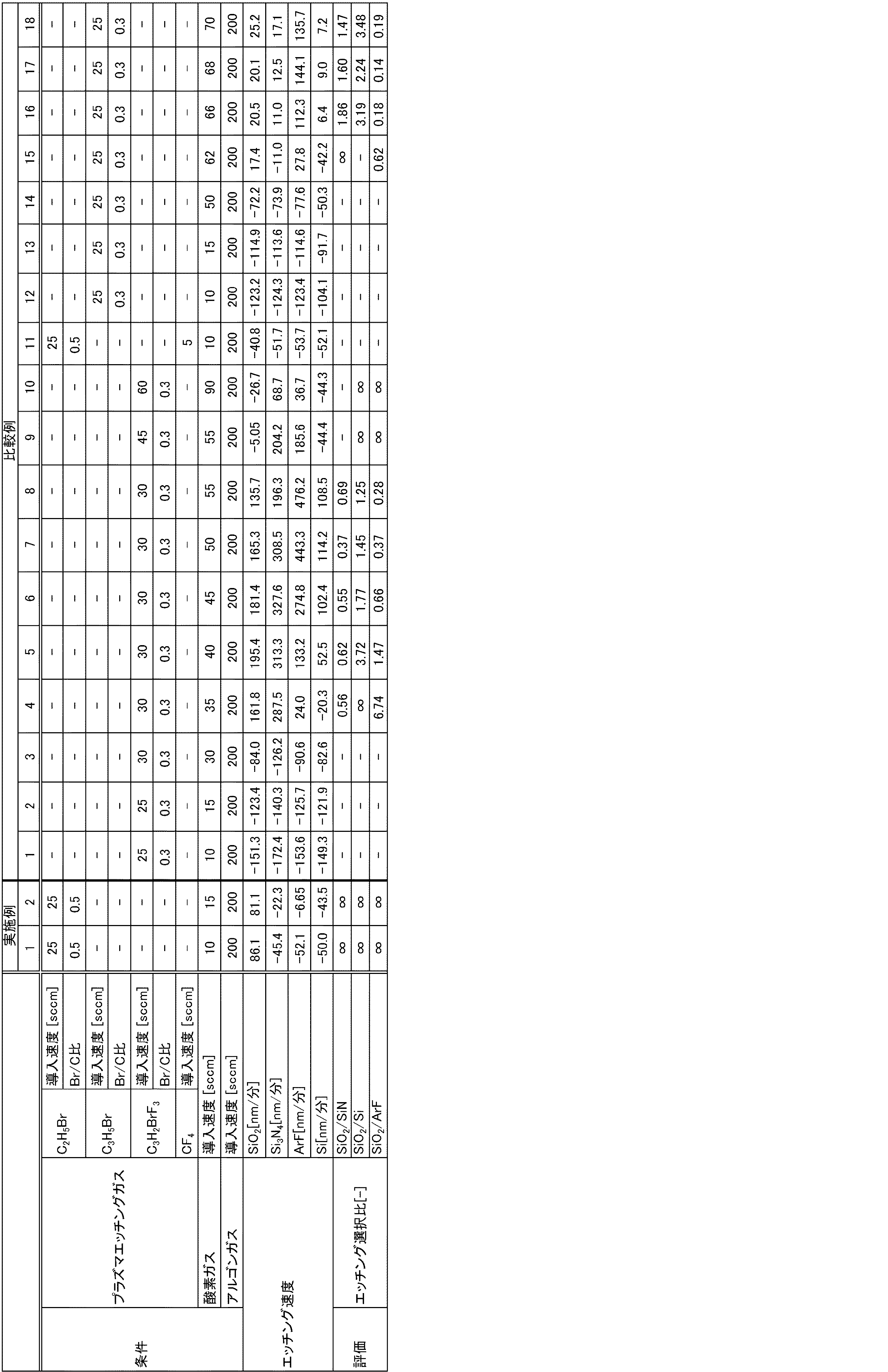
表1より、以下のことが分かる。まず、実施例1〜2のように、臭素原子数/炭素原子数の比率が0.5でありフッ素原子を含有しないブロモエタンガスをプラズマエッチングガスとして用いた場合、全ての非加工対象に対するシリコン酸化膜のエッチング選択比が無限大となっており、高選択的にシリコン酸化膜をエッチングできたことが分かる。一方、フッ素原子を含有する、及び/又は、臭素原子数/炭素原子数の比率が0.4未満である臭素化合物を含有するプラズマエッチングガスを用いた比較例1〜18では、シリコン窒化膜に対するシリコン酸化膜のエッチング選択比が2未満であるか、或いは、Si膜及び/又はArF膜に対するシリコン酸化膜のエッチング選択比が2未満であり、シリコン酸化膜を高選択的にエッチングできなかったことが分かる。
特に、比較例1〜10の臭素原子数/炭素原子数の比率が0.3である、2‐ブロモ‐3,3,3,‐トリフルオロプロペンガスをプラズマエッチングガスとして用いた場合では、加工対象であるシリコン酸化膜上に堆積膜が堆積する、又は、シリコン酸化膜のエッチング速度に対して、シリコン窒化膜のエッチング速度が同等かそれ以上となるため、シリコン酸化膜が選択的にエッチングできないことがわかる。
また、比較例11にて使用した臭素原子数/炭素原子数の比率が0.5であるブロモエタンガスと、少量の四フッ化炭素とを含むプラズマエッチングガスでは、加工対象であるシリコン酸化膜上にも堆積膜が堆積するため、シリコン酸化膜が選択的にエッチングできないことがわかる。
さらに、フッ素を含有せず、臭素原子数/炭素原子数の比率が0.3である2‐ブロモ‐1‐プロペンガスをプラズマエッチングガスとして用いた比較例12〜14、16〜18では、加工対象であるシリコン酸化膜上に堆積膜が堆積するか、又は、シリコン窒化膜のエッチング速度も比較的早くなるためにエッチング選択比の値が2未満と低く、シリコン酸化膜を選択的にエッチングできなかったことが分かる。
特に、2‐ブロモ‐1‐プロペンガスをプラズマエッチングガスとして用いた比較例15では、シリコン窒化膜に対するシリコン酸化膜のエッチング選択比は良好であるが、Si膜及びArF膜に対してシリコン酸化膜を選択的にエッチングすることができなかったことが分かる。
Table 1 shows the following. First, as in Examples 1 and 2, when a bromoethane gas having a bromine atom / carbon atom ratio of 0.5 and containing no fluorine atoms is used as a plasma etching gas, silicon for all non-processing objects is used. It can be seen that the etching selectivity of the oxide film is infinite, and the silicon oxide film can be etched with high selectivity. On the other hand, in Comparative Examples 1 to 18 using a plasma etching gas containing a fluorine atom and / or containing a bromine compound having a bromine atom / carbon atom ratio of less than 0.4, the silicon nitride film The etching selectivity of the silicon oxide film is less than 2, or the etching selectivity of the silicon oxide film to the Si film and / or ArF film is less than 2, and the silicon oxide film could not be etched with high selectivity. I understand.
In particular, in the case where 2-bromo-3,3,3, -trifluoropropene gas having a bromine atom number / carbon atom ratio of Comparative Examples 1 to 10 is 0.3, the plasma etching gas is processed. The deposited film is deposited on the target silicon oxide film, or the etching speed of the silicon nitride film is equal to or higher than the etching speed of the silicon oxide film, so that the silicon oxide film cannot be selectively etched. I understand that.
In addition, in the plasma etching gas containing the bromoethane gas having a bromine / carbon atom ratio of 0.5 and a small amount of carbon tetrafluoride used in Comparative Example 11, the silicon oxide film to be processed is used. It can be seen that the silicon oxide film cannot be selectively etched because the deposited film is also deposited on the top.
Further, in Comparative Examples 12 to 14 and 16 to 18 in which 2-bromo-1-propene gas containing no fluorine and having a bromine atom / carbon atom ratio of 0.3 was used as a plasma etching gas, The deposited film is deposited on the target silicon oxide film, or the etching speed of the silicon nitride film is relatively high, so the etching selectivity value is low as less than 2, and the silicon oxide film can be selectively etched. You can see that there wasn't.
In particular, in Comparative Example 15 using 2-bromo-1-propene gas as the plasma etching gas, the etching selectivity of the silicon oxide film to the silicon nitride film is good, but the silicon oxide film is compared to the Si film and ArF film. It can be seen that the film could not be selectively etched.
本発明によれば、シリコン酸化膜を高選択的にエッチングすることができる。 According to the present invention, the silicon oxide film can be etched with high selectivity.
Claims (4)
処理容器内に前記被処理体を載置する準備工程と、
臭素原子数/炭素原子数の比率が0.4以上1.0以下である臭素化合物を含有し、且つ、フッ素原子を含有しないプラズマエッチングガスのプラズマにより、前記被処理体上の前記シリコン酸化膜をプラズマエッチングするエッチング工程と、を含み、
前記シリコン酸化膜の前記シリコン窒化膜に対するエッチング選択比が2以上であり、且つ、前記シリコン酸化膜の有機膜及び/又は無機膜に対するエッチング選択比が2以上である、
プラズマエッチング方法。 A plasma etching method for plasma etching a target object having a silicon oxide film and a silicon nitride film,
A preparation step of placing the object to be processed in a processing container;
The silicon oxide film on the object to be processed by plasma of a plasma etching gas containing a bromine compound having a ratio of bromine atoms / carbon atoms of 0.4 to 1.0 and not containing fluorine atoms An etching process for plasma etching,
The etching selectivity of the silicon oxide film to the silicon nitride film is 2 or more, and the etching selectivity ratio of the silicon oxide film to the organic film and / or inorganic film is 2 or more.
Plasma etching method .
Priority Applications (1)
| Application Number | Priority Date | Filing Date | Title |
|---|---|---|---|
| JP2016068937A JP6569578B2 (en) | 2016-03-30 | 2016-03-30 | Plasma etching method |
Applications Claiming Priority (1)
| Application Number | Priority Date | Filing Date | Title |
|---|---|---|---|
| JP2016068937A JP6569578B2 (en) | 2016-03-30 | 2016-03-30 | Plasma etching method |
Publications (2)
| Publication Number | Publication Date |
|---|---|
| JP2017183534A JP2017183534A (en) | 2017-10-05 |
| JP6569578B2 true JP6569578B2 (en) | 2019-09-04 |
Family
ID=60007266
Family Applications (1)
| Application Number | Title | Priority Date | Filing Date |
|---|---|---|---|
| JP2016068937A Active JP6569578B2 (en) | 2016-03-30 | 2016-03-30 | Plasma etching method |
Country Status (1)
| Country | Link |
|---|---|
| JP (1) | JP6569578B2 (en) |
Families Citing this family (1)
| Publication number | Priority date | Publication date | Assignee | Title |
|---|---|---|---|---|
| WO2023100476A1 (en) * | 2021-12-02 | 2023-06-08 | 株式会社レゾナック | Method for forming deposition film |
Family Cites Families (4)
| Publication number | Priority date | Publication date | Assignee | Title |
|---|---|---|---|---|
| KR100230981B1 (en) * | 1996-05-08 | 1999-11-15 | 김광호 | Plasma etching method for manufacturing process of semiconductor device |
| JP2000208488A (en) * | 1999-01-12 | 2000-07-28 | Kawasaki Steel Corp | Etching method |
| JP4515956B2 (en) * | 2005-05-02 | 2010-08-04 | 株式会社日立ハイテクノロジーズ | Sample etching method |
| US8512586B2 (en) * | 2011-09-01 | 2013-08-20 | Tel Epion Inc. | Gas cluster ion beam etching process for achieving target etch process metrics for multiple materials |
-
2016
- 2016-03-30 JP JP2016068937A patent/JP6569578B2/en active Active
Also Published As
| Publication number | Publication date |
|---|---|
| JP2017183534A (en) | 2017-10-05 |
Similar Documents
| Publication | Publication Date | Title |
|---|---|---|
| TWI670768B (en) | Plasma etching method | |
| KR100874813B1 (en) | Dry etching gas and dry etching method | |
| JP5850043B2 (en) | Etching gas and etching method | |
| KR102340870B1 (en) | Plasma Etching Method | |
| CN109564868B (en) | Plasma etching method | |
| WO2020195559A1 (en) | Dry etching method and method for producing semiconductor device | |
| JP6569578B2 (en) | Plasma etching method | |
| WO2017159512A1 (en) | Plasma etching method | |
| JP2017050413A (en) | Plasma etching method | |
| US10497580B2 (en) | Plasma etching method | |
| WO2016117563A1 (en) | Plasma etching method | |
| JP2012043869A (en) | Etching gas and etching method | |
| JP2018032667A (en) | Plasma etching method | |
| WO2023074511A1 (en) | Etching gas and etching method using same | |
| JP2014192322A (en) | Etching method |
Legal Events
| Date | Code | Title | Description |
|---|---|---|---|
| A621 | Written request for application examination |
Free format text: JAPANESE INTERMEDIATE CODE: A621 Effective date: 20181001 |
|
| A131 | Notification of reasons for refusal |
Free format text: JAPANESE INTERMEDIATE CODE: A131 Effective date: 20190416 |
|
| A977 | Report on retrieval |
Free format text: JAPANESE INTERMEDIATE CODE: A971007 Effective date: 20190418 |
|
| A521 | Request for written amendment filed |
Free format text: JAPANESE INTERMEDIATE CODE: A523 Effective date: 20190529 |
|
| TRDD | Decision of grant or rejection written | ||
| A01 | Written decision to grant a patent or to grant a registration (utility model) |
Free format text: JAPANESE INTERMEDIATE CODE: A01 Effective date: 20190709 |
|
| A61 | First payment of annual fees (during grant procedure) |
Free format text: JAPANESE INTERMEDIATE CODE: A61 Effective date: 20190722 |
|
| R150 | Certificate of patent or registration of utility model |
Ref document number: 6569578 Country of ref document: JP Free format text: JAPANESE INTERMEDIATE CODE: R150 |
|
| R250 | Receipt of annual fees |
Free format text: JAPANESE INTERMEDIATE CODE: R250 |
|
| R250 | Receipt of annual fees |
Free format text: JAPANESE INTERMEDIATE CODE: R250 |