JP6568743B2 - Conductive noise suppression circuit and inverter device - Google Patents
Conductive noise suppression circuit and inverter device Download PDFInfo
- Publication number
- JP6568743B2 JP6568743B2 JP2015159672A JP2015159672A JP6568743B2 JP 6568743 B2 JP6568743 B2 JP 6568743B2 JP 2015159672 A JP2015159672 A JP 2015159672A JP 2015159672 A JP2015159672 A JP 2015159672A JP 6568743 B2 JP6568743 B2 JP 6568743B2
- Authority
- JP
- Japan
- Prior art keywords
- unit
- coil
- power supply
- common mode
- phase
- Prior art date
- Legal status (The legal status is an assumption and is not a legal conclusion. Google has not performed a legal analysis and makes no representation as to the accuracy of the status listed.)
- Active
Links
- 230000001629 suppression Effects 0.000 title claims description 51
- 239000003990 capacitor Substances 0.000 claims description 67
- 238000001514 detection method Methods 0.000 claims description 52
- 230000003321 amplification Effects 0.000 claims description 21
- 238000003199 nucleic acid amplification method Methods 0.000 claims description 21
- 238000009499 grossing Methods 0.000 claims description 15
- 230000008878 coupling Effects 0.000 claims description 5
- 238000010168 coupling process Methods 0.000 claims description 5
- 238000005859 coupling reaction Methods 0.000 claims description 5
- 230000018199 S phase Effects 0.000 description 20
- 229910001219 R-phase Inorganic materials 0.000 description 16
- 238000004804 winding Methods 0.000 description 7
- 238000010586 diagram Methods 0.000 description 6
- XEEYBQQBJWHFJM-UHFFFAOYSA-N Iron Chemical group [Fe] XEEYBQQBJWHFJM-UHFFFAOYSA-N 0.000 description 4
- 230000008859 change Effects 0.000 description 3
- 230000004907 flux Effects 0.000 description 3
- 230000001276 controlling effect Effects 0.000 description 2
- 230000009467 reduction Effects 0.000 description 2
- 239000004065 semiconductor Substances 0.000 description 2
- XUIMIQQOPSSXEZ-UHFFFAOYSA-N Silicon Chemical compound [Si] XUIMIQQOPSSXEZ-UHFFFAOYSA-N 0.000 description 1
- 235000010724 Wisteria floribunda Nutrition 0.000 description 1
- 230000008901 benefit Effects 0.000 description 1
- 239000004020 conductor Substances 0.000 description 1
- 238000005516 engineering process Methods 0.000 description 1
- 239000000696 magnetic material Substances 0.000 description 1
- 238000004519 manufacturing process Methods 0.000 description 1
- 238000005259 measurement Methods 0.000 description 1
- 230000004048 modification Effects 0.000 description 1
- 238000012986 modification Methods 0.000 description 1
- 230000007935 neutral effect Effects 0.000 description 1
- ZYHMJXZULPZUED-UHFFFAOYSA-N propargite Chemical compound C1=CC(C(C)(C)C)=CC=C1OC1C(OS(=O)OCC#C)CCCC1 ZYHMJXZULPZUED-UHFFFAOYSA-N 0.000 description 1
- 230000010349 pulsation Effects 0.000 description 1
- 230000001105 regulatory effect Effects 0.000 description 1
- 229910052710 silicon Inorganic materials 0.000 description 1
- 239000010703 silicon Substances 0.000 description 1
- 238000011144 upstream manufacturing Methods 0.000 description 1
- 229910000859 α-Fe Inorganic materials 0.000 description 1
Images


Landscapes
- Engineering & Computer Science (AREA)
- Power Engineering (AREA)
- Inverter Devices (AREA)
- Physics & Mathematics (AREA)
- Electromagnetism (AREA)
- Power Conversion In General (AREA)
Description
本発明は、伝導性ノイズ抑制回路及びインバータ装置に関する。 The present invention relates to a conductive noise suppression circuit and an inverter device.
モータなどを制御するために用いられるインバータ装置は、ダイオードブリッジやスイッチング素子などによって商用の交流電圧を直流電圧に変換する整流部を備えている。そして、インバータ装置は、変換された直流電圧を、スイッチング素子によって交流電圧に変換するインバータ部を備えている。 An inverter device used for controlling a motor or the like includes a rectifier that converts a commercial AC voltage into a DC voltage using a diode bridge, a switching element, or the like. And the inverter apparatus is provided with the inverter part which converts the converted DC voltage into an AC voltage by a switching element.
このようなインバータ装置は、スイッチング素子の動作などに起因して、電源線を伝わって他の電子機器に影響を与える伝導性ノイズを発生する。伝導性ノイズには、電源線間で往復するノーマルモードノイズ(ディファレンシャルモードノイズ)と、電源線と接地(アース)との間を伝わるコモンモードノイズとがある。 Such an inverter device generates conductive noise that travels through the power supply line and affects other electronic devices due to the operation of the switching element. Conductive noise includes normal mode noise (differential mode noise) reciprocating between power supply lines and common mode noise transmitted between the power supply line and ground (earth).
特許文献1には、交流電源の出力を直流電圧に変換する整流器と、電力用半導体素子のスイッチング動作により直流電圧を交流電圧に変換する電力変換器とを有する系に適用される伝導性ノイズフィルタであって、電力用半導体素子のスイッチング動作時に発生するコモンモード電圧を、交流電源と整流器間の線路に接続された接地コンデンサを介して検出するコモンモード電圧検出手段と、検出したコモンモード電圧に基づいて、コモンモード電圧と同じ大きさの逆極性の相殺用電圧を発生し、この相殺用電圧を線路における交流電源と接地コンデンサの接続点との間に重畳させてコモンモード電圧を相殺する相殺用電圧源とを備える伝導性ノイズフィルタが記載されている。
特許文献2には、ハイブリッド車などの高電圧モータとそれを駆動する三相インバータ回路とからなる車載用高電圧モータ装置のコモンモード電流をコモンモードノイズ検出回路により検出し、検出した電気信号によりコモンモードノイズキャンセル回路を駆動してコモンモードノイズキャンセル電圧を発生させ、発生したコモンモードノイズキャンセル電圧は出力コンデンサを通じて車載用高電圧モータ装置に加えられ、これによりコモンモード電流がキャンセルされる車載用高電圧モータ装置用コモンモードノイズキャンセル回路装置が記載されている。
In
特許文献3には、検出トランスと、フィルタ装置と、電圧増幅器と、電圧印加手段とを備え、検出トランスは、主巻線と、主巻線が巻回される共通鉄心と、共通鉄心の内側に配置され各主巻線間を仕切る漏れ磁束用鉄心と、共通鉄心に均等に巻回されて主巻線に流れる電流を検出する検出巻線とを有し、漏れ磁束用鉄心には主巻線を流れるノーマルモード電流により磁束が生じてノーマルモード電流に対するインダクタンスとして作用し、共通鉄心にはノーマルモード電流と主巻線を流れるコモンモード電流により磁束が生じてコモンモード電流に対するインダクタンスとして作用する高周波電流低減装置が記載されている。 Patent Document 3 includes a detection transformer, a filter device, a voltage amplifier, and voltage application means. The detection transformer includes a main winding, a common iron core around which the main winding is wound, and an inner side of the common iron core. And a magnetic flux leakage core that separates the main windings and a detection winding that is wound evenly around the common iron core and detects the current flowing through the main winding. Magnetic flux is generated by the normal mode current flowing through the wire and acts as an inductance for the normal mode current, and the common core generates a magnetic flux by the normal mode current and the common mode current flowing through the main winding, and acts as an inductance for the common mode current. A current reduction device is described.
非特許文献1には、コモンモードトランスをLISNとインバータの間に挿入し、接地コンデンサでのコモンモード電圧変動を検出し、これと逆極性の電圧をコモンモードトランスに発生させることにより、電源側への漏れ電流を原理的には完全に抑制することができる低電圧化電圧型アクティブフィルタが記載されている。
In
ところで、伝導性ノイズのレベルは、国際無線障害特別委員会CISPR(ComiteInternational Special des Perturbations Radioelectriques)の規格により規制されているため、伝導性ノイズを許容値以下に抑制できることが求められる。
本発明の目的は、伝導性ノイズを容易に抑制できる伝導性ノイズ抑制回路等を提供することにある。
By the way, since the level of conductive noise is regulated by the standard of the International Radio Interference Special Committee CISPR (Comite International Special des Perturbations Radioelectriques), it is required to be able to suppress the conductive noise below an allowable value.
The objective of this invention is providing the conductive noise suppression circuit etc. which can suppress conductive noise easily.
かかる目的のもと、本発明が適用される伝導性ノイズ抑制回路は、交流を供給する複数の電源線のそれぞれに直列に設けられ、相互に磁気結合する複数のコイルを有する第1のコイル部を備える。また、伝導性ノイズ抑制回路は、前記第1のコイル部に直列に接続されるとともに、前記複数の電源線のそれぞれに直列に設けられ、相互に磁気結合する複数のコイルを有する第2のコイル部を備える。そして、伝導性ノイズ抑制回路は、前記第1のコイル部と前記第2のコイル部とのいずれか一方に磁気結合してコモンモードノイズを検出する検出コイルを備える。そしてまた、伝導性ノイズ抑制回路は、前記検出コイルが検出したコモンモードノイズに対応する信号を増幅する増幅部を備える。さらに、前記第1のコイル部と前記第2のコイル部との間において前記複数の電源線のそれぞれに接続され、前記増幅部からの出力を当該複数の電源線のそれぞれに重畳する複数のコンデンサを有するコンデンサ部とを備える。さらにまた、前記コンデンサ部の有する前記複数のコンデンサのそれぞれの一方の端子は対応する前記複数の電源線のそれぞれに接続され、当該複数のコンデンサのそれぞれの他方の端子は共通に前記増幅部の出力端子のみに接続されている。 For this purpose, the conductive noise suppression circuit to which the present invention is applied is provided in series with each of a plurality of power supply lines that supply alternating current, and has a first coil portion that has a plurality of coils that are magnetically coupled to each other. Is provided. The conductive noise suppression circuit is connected in series to the first coil unit, and is provided in series with each of the plurality of power supply lines, and has a plurality of coils that are magnetically coupled to each other. A part. The conductive noise suppression circuit includes a detection coil that magnetically couples to one of the first coil portion and the second coil portion to detect common mode noise. The conductive noise suppression circuit further includes an amplifying unit that amplifies a signal corresponding to the common mode noise detected by the detection coil. Furthermore, a plurality of capacitors connected to each of the plurality of power supply lines between the first coil unit and the second coil unit, and superimposing an output from the amplification unit on each of the plurality of power supply lines And a capacitor portion. Furthermore, one terminal of each of the plurality of capacitors included in the capacitor unit is connected to each of the corresponding plurality of power supply lines, and each other terminal of the plurality of capacitors is commonly used as an output of the amplifier unit. Only connected to the terminal.
このような伝導性ノイズ抑制回路において、前記第1のコイル部と前記第2のコイル部とのいずれか他方に磁気的に結合してコモンモードノイズを検出するとともに、前記検出コイルと直列接続される他の検出コイルをさらに備えることを特徴とすることができる。 In such a conductive noise suppression circuit, common mode noise is detected by being magnetically coupled to one of the first coil portion and the second coil portion, and is connected in series with the detection coil. It is possible to further include another detection coil.
これにより、検出するコモンモードノイズの信号が大きくできる。 Thereby, the signal of the common mode noise to detect can be enlarged.
また、前記第1のコイル部のコイルと前記第2のコイル部のコイルとは、トロイダルコアに巻き回されたタップ付導線で構成されていることを特徴とすることができる。 Moreover, the coil of the said 1st coil part and the coil of the said 2nd coil part are comprised by the conducting wire with a tap wound by the toroidal core, It can be characterized by the above-mentioned.
これにより、伝導性ノイズ抑制回路が小型化できる。 Thereby, a conductive noise suppression circuit can be reduced in size.
さらに、前記増幅部は、電流増幅器を備えることを特徴とすることができる。 The amplifying unit may include a current amplifier.
これにより、コモンモードノイズの相殺が容易にできる。 Thereby, the common mode noise can be easily canceled.
また、他の観点からとらえると、本発明が適用されるインバータ装置は、交流を直流に整流する整流部と、前記整流部から出力される直流電圧を平滑化する平滑化部と、を備える。また、インバータ装置は、負荷に接続され、前記平滑化部により平滑化された直流を交流に変換して当該負荷へ出力するインバータ部と、前記整流部又は前記インバータ部において設けられ、伝導性ノイズを抑制する抑制部と、を備える。そして、前記抑制部が、交流を供給する複数の電源線のそれぞれに直列に設けられ、相互に磁気結合する複数のコイルを有する第1のコイル部を備える。また、抑制部は、前記第1のコイル部に直列に接続されるとともに、前記複数の電源線のそれぞれに直列に設けられ、相互に磁気結合する複数のコイルを有する第2のコイル部を備える。そして、抑制部は、前記第1のコイル部と前記第2のコイル部とのいずれか一方に磁気結合してコモンモードノイズを検出する検出コイルを備える。そしてまた、抑制部は、前記検出コイルが検出したコモンモードノイズに対応する信号を増幅する増幅部を備える。さらに、抑制部は、前記第1のコイル部と前記第2のコイル部との間において前記複数の電源線のそれぞれに接続され、前記増幅部からの出力を当該複数の電源線のそれぞれに重畳する複数のコンデンサを有するコンデンサ部を備える。さらにまた、前記コンデンサ部の有する前記複数のコンデンサのそれぞれの一方の端子は対応する前記複数の電源線のそれぞれに接続され、当該複数のコンデンサのそれぞれの他方の端子は共通に前記増幅部の出力端子のみに接続されている。 From another point of view, the inverter device to which the present invention is applied includes a rectifying unit that rectifies alternating current into direct current, and a smoothing unit that smoothes the direct-current voltage output from the rectifying unit. The inverter device is connected to a load, and is provided in the inverter unit that converts the direct current smoothed by the smoothing unit into alternating current and outputs the alternating current, and the rectifying unit or the inverter unit. A suppression unit that suppresses. And the said suppression part is provided in series with each of the several power wire which supplies alternating current, and is provided with the 1st coil part which has several coils which carry out magnetic coupling mutually. The suppression unit includes a second coil unit that is connected in series to the first coil unit and that is provided in series with each of the plurality of power supply lines and includes a plurality of coils that are magnetically coupled to each other. . The suppression unit includes a detection coil that detects common mode noise by being magnetically coupled to one of the first coil unit and the second coil unit. In addition, the suppression unit includes an amplification unit that amplifies a signal corresponding to the common mode noise detected by the detection coil. Furthermore, the suppression unit is connected to each of the plurality of power supply lines between the first coil unit and the second coil unit, and the output from the amplification unit is superimposed on each of the plurality of power supply lines. A capacitor unit having a plurality of capacitors. Furthermore, one terminal of each of the plurality of capacitors included in the capacitor unit is connected to each of the corresponding plurality of power supply lines, and each other terminal of the plurality of capacitors is commonly used as an output of the amplifier unit. Only connected to the terminal.
本発明によれば、伝導性ノイズを容易に抑制できる伝導性ノイズ抑制回路等を提供できる。 ADVANTAGE OF THE INVENTION According to this invention, the conductive noise suppression circuit etc. which can suppress conductive noise easily can be provided.
以下、添付図面を参照して、本発明の実施の形態について詳細に説明する。本発明の実施の形態で説明するインバータ装置(回路)は、例えばエアコンや冷蔵庫等の圧縮機に用いられるモータなどに電力を供給するために用いられる。インバータ装置は、商用の交流電源から供給される交流を直流に変換(整流)する。そして、その直流を平滑化した後に、交流に変換する。
ここでは、インバータ装置の負荷としてモータを例として説明するが、モータ以外が負荷であってもよい。
Embodiments of the present invention will be described below in detail with reference to the accompanying drawings. The inverter device (circuit) described in the embodiment of the present invention is used to supply electric power to a motor used in a compressor such as an air conditioner or a refrigerator. The inverter device converts (rectifies) alternating current supplied from a commercial alternating current power source into direct current. And after smoothing the direct current | flow, it converts into alternating current.
Here, a motor is described as an example of the load of the inverter device, but a load other than the motor may be used.
[第1の実施の形態]
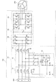
図1は、第1の実施の形態が適用されるインバータ装置100を示す図である。インバータ装置100は、中性相(N相)を備えた三相4線式の交流電源200から交流が供給される。ここでは、第一相から第三相を、R相、S相、T相と表記する。なお、交流電源200からR相、S相、T相及びN相を供給する電源線を、R相、S相、T相及びN相の電源線と表記する。相を区別しない場合は電源線と表記する。また、後述する第1のコイル部11及び第2のコイル部13が直列に接続されていても同様に電源線と表記する。
[First Embodiment]
FIG. 1 is a diagram showing an
ここでは、インバータ装置100は、負荷として三相交流で制御されるモータ300に接続されているとする。モータ300は、例えば、DCブラシレスモータである。なお、モータ300は、他の三相交流モータであってもよい。
Here, it is assumed that the
インバータ装置100は、伝導性ノイズを抑制する抑制部10、交流電源200から供給される交流を直流に整流する整流部20を備える。また、インバータ装置100は、整流部20から出力された直流を平滑化する平滑化部30を備える。そして、インバータ装置100は、平滑化された直流を三相交流に変換して、モータ300に供給するインバータ部40を備える。
なお、図1に示すように、一部の端子は接地されている。
The
As shown in FIG. 1, some terminals are grounded.
インバータ装置100において、交流電源200側から抑制部10、整流部20、平滑化部30、インバータ部40の順に接続されている。そして、インバータ部40がモータ300に接続されている。
In the
抑制部10は、伝導性ノイズを抑制する。抑制部10については、後述する。
The
整流部20は、例えば6つの整流ダイオードD1〜D6から構成されるダイオードブリッジを備える。6つの整流ダイオードD1〜D6は、交流電源200から供給される交流を直流に整流する。整流ダイオードD1〜D6をそれぞれ区別しないときは、整流ダイオードDと表記する。
The
平滑化部30は、平滑コンデンサ(平滑キャパシタ)Csを備える。平滑コンデンサCsは、整流部20が整流した直流の高電圧側の配線(図1における上側の配線)と基準電圧側の配線(図1における下側の配線)との間に接続されている。
The smoothing
インバータ部40は、スイッチング素子Stと帰還ダイオードDfとをそれぞれ有する6つのスイッチング回路SC1〜SC6を備える。なお、スイッチング回路SC1〜SC6を区別しない場合には、スイッチング回路SCと表記する。
そして、上アームのスイッチング回路SC1と下アームのスイッチング回路SC2とが直列接続され、接続点がモータ300の端子に接続されている。そして、直列接続された上アームのスイッチング回路SC1と下アームのスイッチング回路SC2は、高電圧側の配線と基準電圧側の配線との間に設けられている。他のスイッチング回路SC3〜SC6も同様である。
なお、スイッチング素子Stには、例えば絶縁ゲートバイポーラトランジスタ(IGBT(Insulated Gate Bipolar Transistor))などを用いうる。
The
The upper arm switching circuit SC1 and the lower arm switching circuit SC2 are connected in series, and the connection point is connected to the terminal of the
For example, an insulated gate bipolar transistor (IGBT) can be used as the switching element St.
ここで、第1の実施の形態が適用されるインバータ装置100の動作を説明する。
商用の交流電源200は、伝導性ノイズを抑制する抑制部10を介して、交流電圧を整流部20に供給する。整流部20は、ブリッジ状に接続された整流ダイオードD1〜D6により、交流電源200から供給された交流電圧を直流電圧に整流する。平滑化部30は、平滑コンデンサCsにより、整流部20で整流された直流電圧の脈動を平滑化する。インバータ部40は、スイッチング回路SCにおけるスイッチング素子Stのオン・オフの制御により、モータ300に対して交流電圧を供給する。
Here, the operation of the
The commercial
(抑制部10)
以下では、抑制部10を説明する。抑制部10は、コモンモードノイズを検出し、フィードバックして抑制するアクティブ型の伝導性ノイズ抑制回路である。なお、電力が供給される方向において、抑制部10に対して、交流電源200側を上流側、整流部20側を下流側と表記する。
(Suppression unit 10)
Below, the
抑制部10は、第1のコイル部11、検出コイルL1A、コンデンサ部12、第2のコイル部13及び増幅部14を備える。第1のコイル部11、コンデンサ部12、第2のコイル部13は、交流電源200側から、この順に接続されている。なお、第1のコイル部11が交流電源200に接続され、第2のコイル部13が整流部20に接続されている。そして、検出コイルL1Aが、第1のコイル部11と磁気的に結合するように設けられている。
The
第1のコイル部11は、R相、S相、T相、N相の電源線毎に直列に接続されたコイル(巻線)L1R、L1S、L1T、L1Nを備える。ここでは、コイルL1R、L1S、L1T、L1Nをそれぞれ区別しないときは、コイルL1と表記する。
ここで、コイルとは、インダクタを構成するように螺旋(ループ)状に巻かれた導線をいう。
The
Here, the coil refers to a conductive wire wound in a spiral shape so as to constitute an inductor.
これらのコイルL1R、L1S、L1T、L1Nは、電源線の一部を構成する導線(ワイヤ)であって、1個のトロイダルコアに巻き回されて構成されている。トロイダルコアは、例えば、断面が円形の円環状(ドーナツ形状)のフェライトなどの磁性体で構成されている。トロイダルコアは鉄心と呼ばれることがある。なお、トロイダルコアは、円環状でなくともよく、四角形や三角形などの多角形の枠状であってもよい。また、断面形状も四角形や三角形などの形状であってもよい。 These coils L1 R , L1 S , L1 T , and L1 N are conductive wires (wires) that constitute a part of the power supply line, and are wound around one toroidal core. The toroidal core is made of, for example, a magnetic material such as an annular (doughnut-shaped) ferrite having a circular cross section. Toroidal cores are sometimes called iron cores. Note that the toroidal core does not have to be annular, and may be a polygonal frame such as a quadrangle or a triangle. The cross-sectional shape may also be a shape such as a square or a triangle.
そして、コイルL1R、L1S、L1T、L1Nは、1個のトロイダルコアに互いに隣接するように巻き回されている。よって、コイルL1R、L1S、L1T、L1Nは、相互に磁気的に結合(磁気結合)している。なお、コイルL1R、L1S、L1T、L1Nは、図1に“・”で示す極性になるように巻き回されている。 The coils L1 R , L1 S , L1 T and L1 N are wound around one toroidal core so as to be adjacent to each other. Therefore, the coils L1 R , L1 S , L1 T , and L1 N are magnetically coupled (magnetically coupled) to each other. The coils L1 R , L1 S , L1 T , and L1 N are wound so as to have a polarity indicated by “·” in FIG.
そして、検出コイルL1Aは、第1のコイル部11に磁気的に結合(磁気結合)するように設けられている。例えば、検出コイルL1Aは、1個のトロイダルコアにコイルL1R、L1S、L1T、L1Nと隣接するよう巻き回されている。また、1個のトロイダルコアにコイルL1R、L1S、L1T、L1Nが互いに隣接するように巻き回され、検出コイルL1AがコイルL1R、L1S、L1T、L1Nに重なるように巻き回れてもよい。なお、検出コイルL1Aは、図1に“・”で示す極性になるように巻き回されている。
検出コイルL1Aの一方の端子は、接地されている。そして、他方の端子は、後述する増幅部14に接続されている。
Then, the detection coil L1 A is provided so as to magnetically coupled (magnetically coupled) to the
One terminal of the detection coil L1 A is grounded. The other terminal is connected to an amplifying
コイルL1R、L1S、L1T、L1Nは、交流電源200から電流が流れる電源線の一部を構成する。よって、コイルL1R、L1S、L1T、L1Nは、流れる電流に対応した太さの導線(ワイヤ)で構成されている。一方、検出コイルL1Aは、後述するように、コモンモードノイズの電流(以下では、コモンモード電流と表記する。)を検出する。よって、検出コイルL1Aは、コモンモード電流が検出できる太さの導線(ワイヤ)で構成されていればよい。
なお、コイルL1R、L1S、L1T、L1Nは、同じインダクタンスであるとよい。
Coils L1 R , L1 S , L1 T , and L1 N constitute part of a power supply line through which current flows from
Note that the coils L1 R , L1 S , L1 T , and L1 N may have the same inductance.
コモンモード電流は、インバータ部40のスイッチング素子Stのスイッチングにより、モータ300などの浮遊容量を介して、接地に対して漏れた高周波の電流である。よって、コモンモード電流は、R相、S相、T相、N相の電源線と接地(アース)との間で同じ方向に流れる。
インダクタであるコイルL1R、L1S、L1T、L1Nは、高周波信号であるコモンモード電流に対して抵抗として働く。よって、コイルL1R、L1S、L1T、L1Nは、コモンモードノイズを抑制(低減)する。しかし、第1のコイル部11では、コモンモードノイズは除去しきれない。
The common mode current is a high-frequency current that leaks to the ground via the stray capacitance of the
The inductors L1 R , L1 S , L1 T , and L1 N that are inductors function as a resistance against a common mode current that is a high-frequency signal. Therefore, the coils L1 R , L1 S , L1 T , and L1 N suppress (reduce) common mode noise. However, the
コモンモード電流がコイルL1R、L1S、L1T、L1Nに流れると、トロイダルコアを介して検出コイルL1Aにコモンモード電流に比例した電流を誘起する。
すなわち、第1のコイル部11と検出コイルL1Aとは、電流トランスとして機能し、コモンモード電流を検出する検出トランスを構成する。
When the common mode current flows through the coils L1 R , L1 S , L1 T and L1 N , a current proportional to the common mode current is induced in the detection coil L1 A via the toroidal core.
That is, the
なお、ノーマルモードノイズは電源線間で往復するように流れる。よって、トロイダルコアに巻き回されたコイルL1R、L1S、L1T、L1Nは、流れるノーマルモードノイズを互いに打ち消すように機能する。 Note that normal mode noise flows so as to reciprocate between power lines. Therefore, the coils L1 R , L1 S , L1 T , and L1 N wound around the toroidal core function to cancel the normal mode noise that flows.
コンデンサ部12は、コンデンサC1R、C1S、C1T、C1Nを備えている。コンデンサC1R、C1S、C1T、C1Nのそれぞれの一方の端子は、R相、S相、T相、N相のそれぞれの電源線に接続されている。コンデンサC1R、C1S、C1T、C1Nのそれぞれの他方の端子は、後述する増幅部14の出力端子に共通に接続されている。すなわち、増幅部14における演算増幅器141の出力(コモンモードノイズの電流を相殺する電流)が、コンデンサC1R、C1S、C1T、C1Nを介して、R相、S相、T相、N相のそれぞれの電源線に重畳される。ここでは、コンデンサC1R、C1S、C1T、C1Nをそれぞれ区別しないときは、コンデンサC1と表記する。
なお、コンデンサC1R、C1S、C1T、C1Nは、同じ容量であるとよい。
The
The capacitors C1 R , C1 S , C1 T , and C1 N may have the same capacity.
コンデンサC1R、C1S、C1T、C1Nは、R相、S相、T相、N相の電源線間に設けられている。例えば、直列接続されたコンデンサC1RとコンデンサC1Sとが、R相の電源線とS相の電源線との間に設けられている。よって、これらのコンデンサC1R、C1S、C1T、C1Nは、R相、S相、T相、N相の電源線を流れるノーマルモードノイズを互いに打ち消すように機能する。 Capacitors C1 R , C1 S , C1 T , and C1 N are provided between R-phase, S-phase, T-phase, and N-phase power lines. For example, a capacitor C1 R and a capacitor C1 S connected in series are provided between an R-phase power line and an S-phase power line. Therefore, these capacitors C1 R , C1 S , C1 T , and C1 N function to cancel normal mode noises flowing through the R-phase, S-phase, T-phase, and N-phase power lines.
第2のコイル部13は、R相、S相、T相、N相の電源線毎に直列に接続されたコイルL2R、L2S、L2T、L2Nを備える。これらのコイルL2R、L2S、L2T、L2Nは、電源線の一部を構成する導線(ワイヤ)であって、第1のコイル部11と同様に、他の1個のトロイダルコアに巻き回されて構成されている。よって、コイルL2R、L2S、L2T、L2Nは、相互に磁気的に結合(磁気結合)している。なお、コイルL2R、L2S、L2T、L2Nは、図1に“・”で示す極性になるように巻き回されている。ここでは、コイルL2R、L2S、L2T、L2Nをそれぞれ区別しないときは、コイルL2と表記する。
なお、コイルL2R、L2S、L2T、L2Nは、同じインダクタンスであるとよい。
The
The coils L2 R , L2 S , L2 T , and L2 N are preferably the same inductance.
インダクタであるコイルL2R、L2S、L2T、L2Nは、第1のコイル部11と同様に、コモンモード電流に対して抵抗として働く。よって、コイルL2R、L2S、L2T、L2Nは、コモンモードノイズを抑制(低減)する。しかし、第1のコイル部11と同様に、第2のコイル部13でも、コモンモードノイズは除去しきれない。
また、トロイダルコアに巻き回されたコイルL2R、L2S、L2T、L2Nは、ノーマルモードノイズを互いに打ち消すように機能する。
The inductors L2 R , L2 S , L2 T , and L2 N that are inductors function as a resistance against the common mode current, similarly to the
The coils L2 R , L2 S , L2 T , and L2 N wound around the toroidal core function to cancel normal mode noise from each other.
増幅部14は、演算増幅器(オペアンプ)141、抵抗R1、R2、R3及びコンデンサC2、C3を備えている。検出コイルL1Aの他方の端子は、抵抗R1を介して接地されている。
抵抗R1の接地されていない側の端子は、演算増幅器141の非反転入力端子(図1では“+”と表記し、以下では非反転入力端子(+)と表記する。)に接続されている。
The amplifying
The terminal on the ungrounded side of the resistor R1 is connected to a non-inverting input terminal (denoted as “+” in FIG. 1 and denoted as a non-inverting input terminal (+) in the following) of the
コンデンサC2は帰還コンデンサ、抵抗R3は帰還抵抗であって、並列接続されている。そして、コンデンサC2及び抵抗R3のそれぞれの一方の端子は、演算増幅器141の反転入力端子(図1では“−”と表記し、以下では反転入力端子(−)と表記する。)に接続されている。一方、コンデンサC2及び抵抗R3のそれぞれの他方の端子は、演算増幅器141の出力端子に接続されている。そして、演算増幅器141の反転入力端子(−)は、抵抗R2を介して接地されている。さらに、位相を調整するためのコンデンサC3が、演算増幅器141の出力端子と、演算増幅器141の駆動電源端子(不図示)との間に設けられている。ここでは、演算増幅器141は、電流増幅器として構成されている。
The capacitor C2 is a feedback capacitor, and the resistor R3 is a feedback resistor, which are connected in parallel. One terminal of each of the capacitor C2 and the resistor R3 is connected to an inverting input terminal of the operational amplifier 141 (denoted as “−” in FIG. 1 and hereinafter denoted as an inverting input terminal (−)). Yes. On the other hand, the other terminal of each of the capacitor C2 and the resistor R3 is connected to the output terminal of the
抑制部10は、次のように動作する。
まず、第1のコイル部11において、検出コイルL1Aが、R相、S相、T相、N相の電源線におけるコモンモードノイズ(コモンモード電流)を検出する。次に、増幅部14の演算増幅器141が、コモンモード電流を増幅して、コンデンサ部12を介して、R相、S相、T相、N相のそれぞれの電源線に供給(重畳)する。なお、演算増幅器141は、コモンモードノイズを打ち消す(相殺する)ようにコモンモード電流を増幅する。よって、R相、S相、T相、N相の電源線におけるコモンモードノイズが抑制される。
なお、コンデンサ部12のコンデンサC1R、C1S、C1T、C1Nにより、R相、S相、T相、N相のそれぞれの電源線のコモンモードノイズのレベルに対応して、重畳する電流が設定される。
The
First, the
The capacitors C1 R , C1 S , C1 T , and C1 N in the
なお、上記では、増幅部14は、検知されたコモンモード電流を増幅するとしたが、コモンモード電流が変換された電圧(コモンモード電圧)を増幅するようにしてもよい。
In the above description, the
以上説明したように、抑制部10は、伝導性ノイズであるノーマルモードノイズ及びコモンモードノイズを抑制する。
As described above, the
次に、第2のコイル部13の機能について説明する。
図2は、第1の実施の形態が適用されるインバータ装置100における抑制部10及び整流部20のノイズを抑制する周波数帯域における交流等価回路である。図2(a)は、図1に対応した交流等価回路、図2(b)は、増幅部14における演算増幅器141の出力端子から見た交流等価回路である。
コモンモードノイズは、高周波信号(交流的)である。よって、コイルL1、L2は、交流的には抵抗として機能し、コンデンサC1は、交流的には短絡(ショート)となる。また、交流電源200のR相、S相、T相、N相は、交流的には短絡(ショート)となる。そして、整流部20の整流ダイオードDは、交流的には短絡(ショート)となる。
よって、図2(a)、(b)では、コイルL1、L2は抵抗の記号で表記し、コンデンサC1は線で結んでいる。なお、整流部20の整流ダイオードDはそのままダイオードの記号で表記している。
Next, the function of the
FIG. 2 is an AC equivalent circuit in a frequency band that suppresses noise of the
Common mode noise is a high-frequency signal (alternating current). Therefore, the coils L1 and L2 function as resistors in terms of alternating current, and the capacitor C1 is short-circuited (shorted) in terms of alternating current. Further, the R phase, S phase, T phase, and N phase of the
Therefore, in FIGS. 2A and 2B, the coils L1 and L2 are represented by resistance symbols, and the capacitor C1 is connected by a line. Note that the rectifier diode D of the
図2(a)に示すように、増幅部14における演算増幅器141の非反転入力端子(+)には、検出コイルL1A及び抵抗R1が並列接続されている。検出コイルL1Aは、交流的には抵抗として機能する。よって、演算増幅器141の非反転入力端子(+)に対するインピーダンスが高い。よって、第1のコイル部11が検出したコモンモード電流に対応する電圧が高くなる。よって、コモンモード電流に対応する電圧が演算増幅器141に入力されやすくなるとともに、コモンモード電流の変化に追随しやすくなり、コモンモードノイズが精度よく抑制できる。
As shown in FIG. 2 (a), the non-inverting input terminal of the
なお、コモンモードノイズの検出方法として、コンデンサ部12と同様の複数のコンデンサを介して検出することが考えられる。この場合、図2(a)における第1のコイル部11がコンデンサ部12と同様な構成になる。コンデンサは、交流的に短絡(ショート)となるため、演算増幅器141の非反転入力端子(+)に対するインピーダンスが低くなり、コモンモード電流に対応する電圧が低くなってしまう。よって、コモンモード電流に対応する電圧が演算増幅器141に入力されにくく、コモンモード電流の変化に追随しづらい。
そこで、第1の実施の形態が適用される抑制部10では、コモンモードノイズ(コモンモード電流)の検出を、検出コイルL1Aで行っている。このため、演算増幅器141の入力端子(非反転入力端子(+))に対するインピーダンスを高く設定できる。
As a common mode noise detection method, it is conceivable to detect through a plurality of capacitors similar to the
Therefore, the suppressing
一方、図2(b)に示すように、増幅部14における演算増幅器141の出力端子は、第1のコイル部11のコイルL1R、L1S、L1T、L1Nをそれぞれ介して接地される。また、演算増幅器141の出力端子は、第2のコイル部13のコイルL2R、L2S、L2Tのそれぞれと整流部20の整流ダイオードD1〜D6との直列接続を介して接地される。なお、コイルL2Nは、整流ダイオードDを介さずに接地される。
このとき、整流ダイオードD1〜D6は交流的に短絡(ショート)である。しかし、コイルL1R、L1S、L1T、L1N及びコイルL2R、L2S、L2T、L2Nは交流的には抵抗として機能する。よって、演算増幅器141の負荷は、インピーダンスが高い。よって、演算増幅器141の出力端子は、高い電圧でコモンモードノイズを打ち消す(相殺する)電流を出力できる。
On the other hand, as shown in FIG. 2B, the output terminal of the
At this time, the rectifier diodes D1 to D6 are short-circuited in an alternating manner. However, the coils L1 R , L1 S , L1 T , L1 N and the coils L2 R , L2 S , L2 T , L2 N function as resistors in terms of alternating current. Therefore, the load of the
一例として、コモンモードノイズを抑制するために必要な演算増幅器141の出力電圧は、±20V程度である。このとき、出力電流は、±0.3A程度となる。
このような出力電圧及び出力電流は、広く用いられている演算増幅器(オペアンプ)で対応しうる。
As an example, the output voltage of the
Such output voltage and output current can be handled by a widely used operational amplifier (op amp).
なお、コモンモードノイズを打ち消す(相殺する)電流または電圧を、コンデンサC1の代わりに、電源線に直列接続されたインダクタを介して行うことが考えられる。この際、低いインピーダンスの駆動回路(例えばプッシュプル型のトランジスタ回路)で電流を供給すると、インダクタのインダクタンスが変動し、電源線に流れる電流を変動させてしまう。
これに対して、第1の実施の形態が適用される抑制部10では、演算増幅器141の負荷が第1のコイル部11のコイルL1と第2のコイル部13のコイルL2との並列接続となっている。よって、インピーダンスが高い。これにより、電源線に流れる電流に与える影響が抑制されている。
It is conceivable that the current or voltage that cancels (cancels) the common mode noise is performed via an inductor connected in series to the power supply line instead of the capacitor C1. At this time, if a current is supplied by a low-impedance driving circuit (for example, a push-pull transistor circuit), the inductance of the inductor fluctuates and the current flowing through the power supply line fluctuates.
On the other hand, in the
図3は、第1の実施の形態が適用されないインバータ装置110を示す図である。
図3に示すように、第1の実施の形態が適用されないインバータ装置110は、図1のインバータ装置100が備える第2のコイル部13を備えない。さらに、次に説明するように、N相を備えない。よって、N相の電源線などを破線で示す。すなわち、インバータ装置110は、三相3線式の交流電源200により交流が供給される。他の構成は、図1に示した第1の実施の形態が適用されるインバータ装置100と同様であるので、説明を省略する。
FIG. 3 is a diagram illustrating an
As illustrated in FIG. 3, the
図4は、第1の実施の形態が適用されないインバータ装置110の抑制部10及び整流部20のノイズを抑制する周波数帯域における交流等価回路である。図4(a)は、図3に対応した交流等価回路、図4(b)は、増幅部14における演算増幅器141の出力端子から見た交流等価回路である。
図2(a)、(b)と同様に、コイルL1は、交流的には抵抗として機能し、コンデンサC1は、交流的には短絡(ショート)となる。また、交流電源200のR相、S相、T相、N相は、交流的には短絡(ショート)となる。そして、整流部20の整流ダイオードDは、交流的には短絡(ショート)となる。
FIG. 4 is an AC equivalent circuit in a frequency band that suppresses noise in the
Similar to FIGS. 2A and 2B, the coil L1 functions as a resistance in terms of alternating current, and the capacitor C1 is short-circuited in terms of alternating current. Further, the R phase, S phase, T phase, and N phase of the
増幅部14における演算増幅器141の非反転入力端子(+)に関しては、図1、図2(a)に示した第1の実施の形態が適用されるインバータ装置100と同様である。すなわち、演算増幅器141の非反転入力端子(+)に対するインピーダンスが高い。よって、第1のコイル部11において検出されたコモンモード電流に対応する電圧が高くなり、増幅部14の演算増幅器141に入力されやすい。
The non-inverting input terminal (+) of the
一方、図4(b)に示すように、増幅部14における演算増幅器141の出力端子は、整流部20の整流ダイオードD1〜D6を介して接地される。このとき、整流ダイオードD1〜D6は、接地に対して、電流の流れる向きが交互に接続される。よって、演算増幅器141の出力端子からの電圧が正負のいずれであっても、整流ダイオードD1〜D6のいずれかにより順方向で接地される。
例えば、シリコンダイオードの場合、順方向の電圧が低く、30Aの電流を流しても電圧は1.5V程度である。
すなわち、コンデンサ部12を介して、コモンモード電流を打ち消すための電流を供給しようとすると、低電圧で大電流を供給することが必要となる。しかし、広く用いられている演算増幅器141では、例えば1.5Vの電圧で30Aの電流を供給することは難しい。
On the other hand, as shown in FIG. 4B, the output terminal of the
For example, in the case of a silicon diode, the forward voltage is low, and the voltage is about 1.5 V even when a current of 30 A is passed.
That is, if it is attempted to supply a current for canceling the common mode current via the
なお、N相の電源線があると、図4(b)に示すように、演算増幅器141の出力端子が、接地されてしまう。このため、第1の実施の形態が適用されないインバータ装置110では、N相の電源線を用いることができない。
If there is an N-phase power line, the output terminal of the
以上説明したように、第1の実施の形態が適用されるインバータ装置100では、抑制部10は、第1のコイル部11及び第2のコイル部13を備えている。これによって、演算増幅器141の入力端子(非反転入力端子(+))から見たインピーダンスが高い。これにより、検出されたコモンモード電流の変動に対して追随しやすい。よって、精度よくコモンモードノイズが抑制できる。また、演算増幅器141の出力端子から見たインピーダンスが高い。これにより、広く用いられている演算増幅器141が適用できる。
すなわち、コモンモードノイズを含む伝導性ノイズが容易に抑制できる。
As described above, in the
That is, conductive noise including common mode noise can be easily suppressed.
図5は、第1の実施の形態が適用されるインバータ装置100の抑制部10によるコモンモードノイズを説明する図である。図5における縦軸は、擬似電源回路網(LISN:Line Impedance Stabilization Network)のノイズ測定用抵抗の両端の電圧降下である雑音端子電圧(dB(μV))である。横軸は、周波数(MHz)である。また、図5には、国際無線障害特別委員会CISPRにより設定された許容値を示している。
FIG. 5 is a diagram illustrating common mode noise caused by the
第1の実施の形態が適用されるインバータ装置100において、増幅部14は、演算増幅器141を駆動する駆動電源が供給される(オン)と動作し、駆動電源が供給されない(オフ)と動作しない。図5には、演算増幅器141のオンの状態(増幅部オン)とオフの状態(増幅部オフ)とを記載している。
In the
増幅部オンでは、演算増幅器141が動作し、コイルL1Aが検知したコモンモード電流が増幅される。よって、コモンモード電流を打ち消す電流が、コンデンサ部12からR相、S相、T相、N相のそれぞれの電源線に供給(重畳)される。すなわち、増幅部オンでは、抑制部10が動作している。
一方、増幅部オフでは、演算増幅器141は動作せず、コイルL1Aが検知したコモンモード電流が増幅されない。よって、コモンモード電流を打ち消す電流は、コンデンサ部12からR相、S相、T相、N相のそれぞれの電源線に供給(重畳)されない。すなわち、増幅部オフでは、抑制部10が動作していない。
The amplification unit on, the
On the other hand, in the amplification unit off, the
図5において、増幅部オンと増幅部オフとを比較すると、増幅部オフでは、0.5MHz以下の周波数帯において、雑音端子電圧が許容値を超えている。しかし、増幅部オンでは、雑音端子電圧が許容値を下回っている。
第1の実施の形態が適用されるインバータ装置100では、抑制部10により、コモンモードノイズが抑制されている。すなわち、抑制部10により、伝導性ノイズが抑制されている。
In FIG. 5, when the amplification unit on and the amplification unit off are compared, the noise terminal voltage exceeds the allowable value in the frequency band of 0.5 MHz or less when the amplification unit is off. However, when the amplification unit is on, the noise terminal voltage is below the allowable value.
In the
そして、第1の実施の形態が適用されるインバータ装置100では、N相の電源線に係る伝導性ノイズについても、抑制されている。
また、抑制部10における増幅部14の演算増幅器141を、電流増幅器としている。これにより、コモンモード電流を打ち消す(相殺する)電流が制御しやすくしている。
In the
In addition, the
なお、上記においては、検出コイルL1Aを第1のコイル部11に磁気結合させた。しかし、検出コイルL1Aを第2のコイル部13に磁気結合させてもよい。同様に動作する。
In the above, the magnetic coupling is not the detection coils L1 A to the
[第2の実施の形態]
図1に示した第1の実施の形態のインバータ装置100は、三相4線式の交流電源200から交流が供給された。第2の実施の形態のインバータ装置100は、三相3線式の交流電源200から交流が供給される。
図6は、第2の実施の形態が適用されるインバータ装置100を示す図である。
図6に示すように、第2の実施の形態のインバータ装置100は、図1のインバータ装置100において、N相の電源線を備えない。すなわち、三相3線式の交流電源200に対応する。他の構成は、図1に示した第1の実施の形態が適用されるインバータ装置100と同様であるので、同じ符号を付して説明を省略する。
[Second Embodiment]
The
FIG. 6 is a diagram illustrating an
As shown in FIG. 6, the
三相3線式の交流電源200を用いるインバータ装置100でも、第1の実施の形態で説明したように、抑制部10により、伝導性ノイズが抑制される。
Even in the
[第3の実施の形態]
第1の実施の形態が適用されるインバータ装置100及び第2の実施の形態が適用されるインバータ装置100は、三相の交流電源200から交流が供給された。これに対して、第3の実施の形態が適用されるインバータ装置100は、単相2線式の交流電源200から交流が供給される。
図7は、第3の実施の形態が適用されるインバータ装置100を示す図である。
図7に示すように、第3の実施の形態が適用されるインバータ装置100は、図1のインバータ装置100において、R相、S相をX相、Y相とし、T相、N相を備えない。そして、整流部20は、4個の整流ダイオードD1〜D4を備えている。すなわち、単相2線式の交流電源200に対応する。他の構成は、図1に示した第1の実施の形態が適用されるインバータ装置100と同様であるので、同じ符号を付して説明を省略する。なお、RをXに、SをYに置き換えている。
[Third Embodiment]
The
FIG. 7 is a diagram illustrating an
As shown in FIG. 7, the
単相2線式の交流電源200を用いるインバータ装置100でも、第1の実施の形態で説明したように、抑制部10により、伝導性ノイズが抑制される。
Even in the
[第4の実施の形態]
第1の実施の形態が適用されるインバータ装置100では、第1のコイル部11に検出コイルL1Aを磁気結合させた。第4の実施の形態が適用されるインバータ装置100では、抑制部10の第2のコイル部13に検出コイルL2Aをさらに磁気結合させている。検出コイルL2Aもコモンモード電流を検出する。
[Fourth Embodiment]
In the
図8は、第4の実施の形態が適用されるインバータ装置100を示す図である。
図8の第4の実施の形態が適用されるインバータ装置100では、第2のコイル部13に対しても、検出コイルL2Aが追加されている。そして、検出コイルL1Aの一方の端子は、接地されず、検出コイルL2Aの一方の端子と接続されている。そして、検出コイルL2Aの他方の端子が接地されている。
他の構成は、図1に示した第1の実施の形態が適用されるインバータ装置100と同様であるので、同じ符号を付して説明を省略する。
FIG. 8 is a diagram showing an
In the
Other configurations are the same as those of the
このように、検出コイルL1A、L2Aを設けることで、インピーダンスが大きくなり、コモンモード電流に対して取り出される信号が大きくなる。よって、コモンモード電流の変化により追随しやすくなり、コモンモードノイズがより精度よく抑制できる。 Thus, by providing the detection coils L1 A and L2 A , the impedance is increased and the signal taken out with respect to the common mode current is increased. Therefore, it becomes easy to follow the change of the common mode current, and the common mode noise can be suppressed more accurately.
この場合、第1のコイル部11のコイルL1Rと第2のコイル部13のコイルL2Rとを、タップ付導線(ワイヤ)で構成し、一個のトロイダルコアに巻き回す。そして、導線(ワイヤ)の一方を交流電源200側のR相の電源線に接続し、導線(ワイヤ)の他方を負荷側(整流部20を含む下流側)のR相の電源線に接続する。そして、タップにコンデンサC1Rを接続する。他のコイルL1S、L1T、L1N及びコイルL2S、L2T、L2Nも同様とする。そして、検出コイルL1A及び検出コイルL2Aも同様に、導線(ワイヤ)を一個のトロイダルコアに巻き回す。
このようにすることで、第1のコイル部11と第2のコイル部13とを一つにできる。
In this case, a coil L2 R of the coil L1 R and the
By doing in this way, the
なお、コイルL1R、L1S、L1T、L1Nと検出コイルL1Aとを一方のトロイダルコアに巻き回し、コイルL2R、L2S、L2T、L2Nと検出コイルL2Aとを他のトロイダルコアに巻き回してもよい。このようにすることで、第1のコイル部11及び検出コイルL1Aを組み合わせた部品と、第2のコイル部13及び検出コイルL2Aを組み合わせた部品とが同じになる。よって、部品の製造及び管理が容易になる。
The coils L1 R , L1 S , L1 T , L1 N and the detection coil L1 A are wound around one toroidal core, and the coils L2 R , L2 S , L2 T , L2 N and the detection coil L2 A are connected to the other You may wind around a toroidal core. By doing in this way, the component which combined the
なお、第2又は第3の実施の形態が適用されるインバータ装置100の抑制部10の第2のコイル部13に対して検出コイルL2Aを設けてもよい。
It is also possible to provide a detection coil L2 A to the
第1の実施の形態から第4の実施の形態が適用されるインバータ装置100では、交流電源200と整流部20との間に抑制部10を設けた。インバータ部40とインバータ装置100の負荷であるモータ300との間に抑制部10を設けてもよい。すなわち、抑制部10は、交流を供給する電源線に設ければよい。
In the
第1の実施の形態から第4の実施の形態において示したインバータ装置100は、一例である。よって、インバータ装置100は、説明した以外の電子部材(抵抗、コンデンサ、コイルなど)や回路を含んで構成されていてもよい。
The
第1の実施の形態から第4の実施の形態では、インバータ装置100において、伝導性ノイズを抑制する抑制部10を説明した。
しかし、伝導性ノイズを抑制する抑制部10は、インバータ装置100以外の伝導性ノイズを発生する装置に適用されてもよい。
In the first to fourth embodiments, the
However, the
その他、本発明の趣旨に反しない限りにおいて様々な変形や実施の形態の組み合わせを行っても構わない。 In addition, various modifications and combinations of embodiments may be performed without departing from the spirit of the present invention.
10…抑制部、11…第1のコイル部、12…コンデンサ部、13…第2のコイル部、14…増幅部、20…整流部、30…平滑化部、40…インバータ部、100、110…インバータ装置、141…演算増幅器、200…交流電源、300…モータ、C1、C1R、C1S、C1T、C1N、C1X、C1Y、C2、C3…コンデンサ、Cs…平滑コンデンサ、D、D1〜D6…整流ダイオード、Df…帰還ダイオード、L1、L1R、L1S、L1T、L1N、L2、L2R、L2S、L2T、L2N…コイル、L1A、L2A…検出コイル、R1〜R3…抵抗、SC、SC1〜SC6…スイッチング回路、St…スイッチング素子
DESCRIPTION OF
Claims (5)
前記第1のコイル部に直列に接続されるとともに、前記複数の電源線のそれぞれに直列に設けられ、相互に磁気結合する複数のコイルを有する第2のコイル部と、
前記第1のコイル部と前記第2のコイル部とのいずれか一方に磁気結合してコモンモードノイズを検出する検出コイルと、
前記検出コイルが検出したコモンモードノイズに対応する信号を増幅する増幅部と、
前記第1のコイル部と前記第2のコイル部との間において前記複数の電源線のそれぞれに接続され、前記増幅部からの出力を当該複数の電源線のそれぞれに重畳する複数のコンデンサを有するコンデンサ部と、を備え、
前記コンデンサ部の有する前記複数のコンデンサのそれぞれの一方の端子は対応する前記複数の電源線のそれぞれに接続され、当該複数のコンデンサのそれぞれの他方の端子は共通に前記増幅部の出力端子のみに接続されている
伝導性ノイズ抑制回路。 A first coil unit having a plurality of coils provided in series with each of a plurality of power supply lines for supplying alternating current and magnetically coupled to each other;
A second coil unit connected in series to the first coil unit and provided in series with each of the plurality of power supply lines, and having a plurality of coils magnetically coupled to each other;
A detection coil for detecting common mode noise by magnetic coupling to one of the first coil portion and the second coil portion;
An amplifier for amplifying a signal corresponding to the common mode noise detected by the detection coil;
A plurality of capacitors connected to each of the plurality of power supply lines between the first coil unit and the second coil unit and superimposing an output from the amplification unit on each of the plurality of power supply lines; A capacitor portion ;
One terminal of each of the plurality of capacitors included in the capacitor unit is connected to each of the corresponding plurality of power supply lines, and the other terminal of each of the plurality of capacitors is commonly connected only to the output terminal of the amplification unit. Connected conductive noise suppression circuit.
前記整流部から出力される直流電圧を平滑化する平滑化部と、
負荷に接続され、前記平滑化部により平滑化された直流を交流に変換して当該負荷へ出力するインバータ部と、
前記整流部又は前記インバータ部において設けられ、伝導性ノイズを抑制する抑制部と、を備え、
前記抑制部が、
交流を供給する複数の電源線のそれぞれに直列に設けられ、相互に磁気結合する複数のコイルを有する第1のコイル部と、
前記第1のコイル部に直列に接続されるとともに、前記複数の電源線のそれぞれに直列に設けられ、相互に磁気結合する複数のコイルを有する第2のコイル部と、
前記第1のコイル部と前記第2のコイル部とのいずれか一方に磁気結合してコモンモードノイズを検出する検出コイルと、
前記検出コイルが検出したコモンモードノイズに対応する信号を増幅する増幅部と、
前記第1のコイル部と前記第2のコイル部との間において前記複数の電源線のそれぞれに接続され、前記増幅部からの出力を当該複数の電源線のそれぞれに重畳する複数のコンデンサを有するコンデンサ部と、を備え、
前記コンデンサ部の有する前記複数のコンデンサのそれぞれの一方の端子は対応する前記複数の電源線のそれぞれに接続され、当該複数のコンデンサのそれぞれの他方の端子は共通に前記増幅部の出力端子のみに接続されている
ことを特徴とするインバータ装置。 A rectifier that rectifies alternating current into direct current;
A smoothing unit that smoothes a DC voltage output from the rectifying unit;
An inverter unit connected to a load and converting the direct current smoothed by the smoothing unit into alternating current and outputting the alternating current;
Provided in the rectification unit or the inverter unit, and a suppression unit for suppressing conductive noise,
The suppression unit is
A first coil unit having a plurality of coils provided in series with each of a plurality of power supply lines for supplying alternating current and magnetically coupled to each other;
A second coil unit connected in series to the first coil unit and provided in series with each of the plurality of power supply lines, and having a plurality of coils magnetically coupled to each other;
A detection coil for detecting common mode noise by magnetic coupling to one of the first coil portion and the second coil portion;
An amplifier for amplifying a signal corresponding to the common mode noise detected by the detection coil;
A plurality of capacitors connected to each of the plurality of power supply lines between the first coil unit and the second coil unit and superimposing an output from the amplification unit on each of the plurality of power supply lines; A capacitor portion ;
One terminal of each of the plurality of capacitors included in the capacitor unit is connected to each of the corresponding plurality of power supply lines, and the other terminal of each of the plurality of capacitors is commonly connected only to the output terminal of the amplification unit. An inverter device characterized by being connected .
Priority Applications (3)
| Application Number | Priority Date | Filing Date | Title |
|---|---|---|---|
| JP2015159672A JP6568743B2 (en) | 2015-08-12 | 2015-08-12 | Conductive noise suppression circuit and inverter device |
| KR1020160015430A KR102561123B1 (en) | 2015-08-12 | 2016-02-11 | Conduction noise filtering circuit, inverting device and compressor |
| US15/216,355 US10177702B2 (en) | 2015-08-12 | 2016-07-21 | Conduction noise filtering circuit, inverting device, and compressor |
Applications Claiming Priority (1)
| Application Number | Priority Date | Filing Date | Title |
|---|---|---|---|
| JP2015159672A JP6568743B2 (en) | 2015-08-12 | 2015-08-12 | Conductive noise suppression circuit and inverter device |
Publications (2)
| Publication Number | Publication Date |
|---|---|
| JP2017038500A JP2017038500A (en) | 2017-02-16 |
| JP6568743B2 true JP6568743B2 (en) | 2019-08-28 |
Family
ID=58048153
Family Applications (1)
| Application Number | Title | Priority Date | Filing Date |
|---|---|---|---|
| JP2015159672A Active JP6568743B2 (en) | 2015-08-12 | 2015-08-12 | Conductive noise suppression circuit and inverter device |
Country Status (2)
| Country | Link |
|---|---|
| JP (1) | JP6568743B2 (en) |
| KR (1) | KR102561123B1 (en) |
Families Citing this family (12)
| Publication number | Priority date | Publication date | Assignee | Title |
|---|---|---|---|---|
| JP2018148671A (en) * | 2017-03-03 | 2018-09-20 | ダイキン工業株式会社 | Power supply board, power supply unit and refrigerator |
| JP6858070B2 (en) * | 2017-05-08 | 2021-04-14 | 三星電子株式会社Samsung Electronics Co.,Ltd. | Conductive noise suppression device, power conversion device and motor device |
| JP6873892B2 (en) * | 2017-12-22 | 2021-05-19 | パナソニックIpマネジメント株式会社 | Switching power supply |
| KR102034651B1 (en) * | 2018-02-01 | 2019-10-21 | 엘지전자 주식회사 | Power supply of an air conditioner |
| KR101945463B1 (en) * | 2018-05-02 | 2019-02-07 | 울산과학기술원 | A Transformer-Isolated Common-Mode Active EMI Filter without Additional Components on Power Line, and Method for reducing EMI noise using it |
| CN111614094B (en) * | 2019-02-22 | 2023-08-18 | 欧姆龙株式会社 | Electromagnetic interference filter circuit |
| US11996769B2 (en) * | 2020-06-04 | 2024-05-28 | Mitsubishi Electric Corporation | Noise filter |
| EP4181371A4 (en) * | 2020-07-13 | 2023-08-02 | Mitsubishi Electric Corporation | Noise filter |
| JP7295483B2 (en) * | 2021-09-30 | 2023-06-21 | ダイキン工業株式会社 | Noise reduction circuits, load systems, power converters and refrigerators |
| JP7288206B2 (en) * | 2021-09-30 | 2023-06-07 | ダイキン工業株式会社 | Noise reduction circuit, power conversion device and refrigeration device |
| JP7315862B2 (en) * | 2021-09-30 | 2023-07-27 | ダイキン工業株式会社 | Power conversion equipment and refrigeration equipment |
| JP2023105341A (en) * | 2022-01-19 | 2023-07-31 | サンデン株式会社 | Active filter device and electric compressor provided with the same |
Family Cites Families (5)
| Publication number | Priority date | Publication date | Assignee | Title |
|---|---|---|---|---|
| JP2006238310A (en) * | 2005-02-28 | 2006-09-07 | Tdk Corp | Lc composite component and noise suppressing circuit using the same |
| JP5263663B2 (en) * | 2008-08-28 | 2013-08-14 | 富士電機株式会社 | Conductive noise filter |
| WO2011125944A1 (en) * | 2010-04-05 | 2011-10-13 | 三菱電機株式会社 | Leakage current reducing device |
| JP5705144B2 (en) * | 2012-01-27 | 2015-04-22 | 三菱電機株式会社 | High frequency current reduction device and detection transformer |
| JP2014241711A (en) * | 2013-04-19 | 2014-12-25 | シャフナー・エーエムファウ・アクチェンゲゼルシャフト | Active EMC filter |
-
2015
- 2015-08-12 JP JP2015159672A patent/JP6568743B2/en active Active
-
2016
- 2016-02-11 KR KR1020160015430A patent/KR102561123B1/en active IP Right Grant
Also Published As
| Publication number | Publication date |
|---|---|
| KR102561123B1 (en) | 2023-07-28 |
| JP2017038500A (en) | 2017-02-16 |
| KR20170020199A (en) | 2017-02-22 |
Similar Documents
| Publication | Publication Date | Title |
|---|---|---|
| JP6568743B2 (en) | Conductive noise suppression circuit and inverter device | |
| US11088614B2 (en) | Conductive noise suppressor, power converter, and motor device | |
| JP5528543B2 (en) | Leakage current reduction device | |
| CN102342010B (en) | Leakage current reduction device | |
| KR100403541B1 (en) | Active Common Mode EMI Filter for Eliminating Conducted Electromagnetic Interference | |
| CN104901521B (en) | Noise filter | |
| JP2010057268A (en) | Conductive noise filter | |
| EP3109987B1 (en) | Active common mode filter device | |
| JP6783214B2 (en) | Noise reduction device | |
| EP2612427A2 (en) | Circuit arrangement and method for reducing common-mode noise in a switched-mode power supply, and a switched-mode power supply | |
| JP7514074B2 (en) | MOTOR DRIVE HAVING A FILTER INCLUDE A THREE-PHASE DIFFERENTIAL MODE REACTOR EXHIBITING COMMON MODE ATTENUATION - Patent application | |
| US10742154B2 (en) | Motor driving device | |
| JP2001231268A (en) | Power conversion device | |
| JP4835930B2 (en) | Inverter device provided with ground fault detection means | |
| US8319462B2 (en) | Output filter and power conversion apparatus having the same | |
| JP6239468B2 (en) | Medical equipment | |
| JP5141228B2 (en) | Active filter device and power conversion device | |
| JP5070929B2 (en) | Active filter device and power conversion device | |
| JP2009077533A (en) | Active filter device and power converter | |
| JP2012034149A (en) | Power source line filter | |
| WO2023054508A1 (en) | Power conversion device and refrigeration device | |
| JP2024052240A (en) | Common mode current detector and active noise canceller | |
| JP2013102697A (en) | Semiconductor power-conversion device |
Legal Events
| Date | Code | Title | Description |
|---|---|---|---|
| A621 | Written request for application examination |
Free format text: JAPANESE INTERMEDIATE CODE: A621 Effective date: 20180524 |
|
| A977 | Report on retrieval |
Free format text: JAPANESE INTERMEDIATE CODE: A971007 Effective date: 20190320 |
|
| A131 | Notification of reasons for refusal |
Free format text: JAPANESE INTERMEDIATE CODE: A131 Effective date: 20190409 |
|
| A521 | Request for written amendment filed |
Free format text: JAPANESE INTERMEDIATE CODE: A523 Effective date: 20190605 |
|
| TRDD | Decision of grant or rejection written | ||
| A01 | Written decision to grant a patent or to grant a registration (utility model) |
Free format text: JAPANESE INTERMEDIATE CODE: A01 Effective date: 20190730 |
|
| A61 | First payment of annual fees (during grant procedure) |
Free format text: JAPANESE INTERMEDIATE CODE: A61 Effective date: 20190805 |
|
| R150 | Certificate of patent or registration of utility model |
Ref document number: 6568743 Country of ref document: JP Free format text: JAPANESE INTERMEDIATE CODE: R150 |
|
| R250 | Receipt of annual fees |
Free format text: JAPANESE INTERMEDIATE CODE: R250 |
|
| R250 | Receipt of annual fees |
Free format text: JAPANESE INTERMEDIATE CODE: R250 |
|
| R250 | Receipt of annual fees |
Free format text: JAPANESE INTERMEDIATE CODE: R250 |