JP6556736B2 - Sizing multiple sections gated by constraining the voltage drop - Google Patents
Sizing multiple sections gated by constraining the voltage drop Download PDFInfo
- Publication number
- JP6556736B2 JP6556736B2 JP2016546760A JP2016546760A JP6556736B2 JP 6556736 B2 JP6556736 B2 JP 6556736B2 JP 2016546760 A JP2016546760 A JP 2016546760A JP 2016546760 A JP2016546760 A JP 2016546760A JP 6556736 B2 JP6556736 B2 JP 6556736B2
- Authority
- JP
- Japan
- Prior art keywords
- capacitance
- section
- circuit
- sections
- power
- Prior art date
- Legal status (The legal status is an assumption and is not a legal conclusion. Google has not performed a legal analysis and makes no representation as to the accuracy of the status listed.)
- Active
Links
Images


Classifications
-
- G—PHYSICS
- G05—CONTROLLING; REGULATING
- G05B—CONTROL OR REGULATING SYSTEMS IN GENERAL; FUNCTIONAL ELEMENTS OF SUCH SYSTEMS; MONITORING OR TESTING ARRANGEMENTS FOR SUCH SYSTEMS OR ELEMENTS
- G05B13/00—Adaptive control systems, i.e. systems automatically adjusting themselves to have a performance which is optimum according to some preassigned criterion
- G05B13/02—Adaptive control systems, i.e. systems automatically adjusting themselves to have a performance which is optimum according to some preassigned criterion electric
- G05B13/0205—Adaptive control systems, i.e. systems automatically adjusting themselves to have a performance which is optimum according to some preassigned criterion electric not using a model or a simulator of the controlled system
-
- H—ELECTRICITY
- H03—ELECTRONIC CIRCUITRY
- H03K—PULSE TECHNIQUE
- H03K19/00—Logic circuits, i.e. having at least two inputs acting on one output; Inverting circuits
- H03K19/0008—Arrangements for reducing power consumption
- H03K19/0016—Arrangements for reducing power consumption by using a control or a clock signal, e.g. in order to apply power supply
-
- G—PHYSICS
- G01—MEASURING; TESTING
- G01R—MEASURING ELECTRIC VARIABLES; MEASURING MAGNETIC VARIABLES
- G01R19/00—Arrangements for measuring currents or voltages or for indicating presence or sign thereof
- G01R19/0084—Arrangements for measuring currents or voltages or for indicating presence or sign thereof measuring voltage only
-
- G—PHYSICS
- G01—MEASURING; TESTING
- G01R—MEASURING ELECTRIC VARIABLES; MEASURING MAGNETIC VARIABLES
- G01R21/00—Arrangements for measuring electric power or power factor
- G01R21/006—Measuring power factor
-
- G—PHYSICS
- G01—MEASURING; TESTING
- G01R—MEASURING ELECTRIC VARIABLES; MEASURING MAGNETIC VARIABLES
- G01R27/00—Arrangements for measuring resistance, reactance, impedance, or electric characteristics derived therefrom
- G01R27/02—Measuring real or complex resistance, reactance, impedance, or other two-pole characteristics derived therefrom, e.g. time constant
- G01R27/26—Measuring inductance or capacitance; Measuring quality factor, e.g. by using the resonance method; Measuring loss factor; Measuring dielectric constants ; Measuring impedance or related variables
- G01R27/2605—Measuring capacitance
-
- H—ELECTRICITY
- H03—ELECTRONIC CIRCUITRY
- H03K—PULSE TECHNIQUE
- H03K17/00—Electronic switching or gating, i.e. not by contact-making and –breaking
- H03K17/51—Electronic switching or gating, i.e. not by contact-making and –breaking characterised by the components used
- H03K17/56—Electronic switching or gating, i.e. not by contact-making and –breaking characterised by the components used by the use, as active elements, of semiconductor devices
- H03K17/687—Electronic switching or gating, i.e. not by contact-making and –breaking characterised by the components used by the use, as active elements, of semiconductor devices the devices being field-effect transistors
-
- H—ELECTRICITY
- H03—ELECTRONIC CIRCUITRY
- H03K—PULSE TECHNIQUE
- H03K19/00—Logic circuits, i.e. having at least two inputs acting on one output; Inverting circuits
- H03K19/003—Modifications for increasing the reliability for protection
- H03K19/00315—Modifications for increasing the reliability for protection in field-effect transistor circuits
Description
[0001] 本開示の複数の態様は、一般にパワーゲーティング(power gating)に関し、より具体的には、電圧降下(voltage droop)を制約することによって、パワーゲーティングされた複数のセクション(power-gated sections)をサイジング(sizing)することに関する。 [0001] Aspects of the present disclosure relate generally to power gating, and more specifically, power-gated sections by constraining voltage droop. Sizing).
[0002] パワー分配ネットワーク(PDN:power distribution network)は、電力供給装置(power supply)(例えば、バッテリ)から、ダイ上の様々な回路へ電力を分配(distribute)するために使用され得る。電力を節約するために、PDNは、パワーゲーティングを用い得、そこでは、PDNは、ある回路が非アクティブの時、その回路からの電力漏れ(power leakage)を防ぐために、電力供給装置からその回路を切断する。回路のディメンション(dimensions)が、ディープナノメートル範囲へと(into the deep nanometer range)スケールダウンされるにつれ、電力漏れは著しく増加する。故に、パワーゲーティングは、電力消費を低減し、モバイルデバイスのバッテリ寿命を延ばすために、重要性を増してきている。 [0002] A power distribution network (PDN) may be used to distribute power from a power supply (eg, a battery) to various circuits on the die. To save power, the PDN may use power gating, where the PDN removes power from the power supply to prevent power leakage from that circuit when that circuit is inactive. Disconnect. As the circuit dimensions are scaled down into the deep nanometer range, power leakage increases significantly. Therefore, power gating has become increasingly important in order to reduce power consumption and extend the battery life of mobile devices.
[0003] 以下は、1つ以上の実施形態の基本的な理解を提供するために、そのような実施形態の簡略化された概要を提示する。この概要は、考えられる全ての実施形態の広範な概観ではなく、全ての実施形態の重要要素や決定的要素を特定するようにも、何れかまたは全ての実施形態の範囲を定める(delineate)ようにも意図されていない。その唯一の目的は、後に提示されるより詳細な説明への前置きとして、簡略化された形式で1つ以上の実施形態のうちのいくつかの概念を提示することである。 [0003] The following presents a simplified summary of such embodiments in order to provide a basic understanding of one or more embodiments. This summary is not an extensive overview of all possible embodiments, but should delineate any or all embodiments to identify key or critical elements for all embodiments. Also not intended. Its sole purpose is to present some concepts of one or more embodiments in a simplified form as a prelude to the more detailed description that is presented later.
[0004] 第1の態様に従って、ダウンストリーム回路におけるパワーゲーティングされた複数のセクションをサイジングするための方法がここに説明される。この方法は、アップストリーム回路のキャパシタンスと、電圧降下制約条件(a voltage-droop constraint)とに基づいて、第1のセクションに関するキャパシタンスを決定することと、アップストリーム回路のキャパシタンスと、電圧降下制約条件と、第1のセクションに関する決定されたキャパシタンスとに基づいて、第2のセクションに関するキャパシタンスを決定することと、アップストリーム回路のキャパシタンスと、電圧降下制約条件と、第1のおよび第2のセクションに関する決定されたキャパシタンスとに基づいて、第3のセクションに関するキャパシタンスを決定することと、を備える。この方法はまた、第1の、第2の、および第3のセクションの各々のサイズを、それらセクションの各々に関する決定されたキャパシタンスに基づいて決定することを備える。 [0004] According to a first aspect, a method for sizing power-gated sections in a downstream circuit is described herein. The method determines the capacitance for the first section based on the upstream circuit capacitance and a voltage-droop constraint, and the upstream circuit capacitance and voltage drop constraint. And determining the capacitance for the second section based on the determined capacitance for the first section, the capacitance of the upstream circuit, the voltage drop constraint, and for the first and second sections Determining a capacitance for the third section based on the determined capacitance. The method also comprises determining the size of each of the first, second, and third sections based on the determined capacitance for each of the sections.
[0005] 第2の態様は、漸進的に(progressively)サイズが大きくなる複数のセクションを備える回路をパワーアップするための方法に関する。この方法は、回路をパワーアップ(powering up)するための信号を受信することと、その信号に応答して、サイズが大きくなっていく順番で、複数のセクションを連続的に(sequentially)パワーアップすることとを備える。 [0005] A second aspect relates to a method for powering up a circuit comprising a plurality of sections that progressively increase in size. This method sequentially powers up multiple sections in order of increasing size in response to receiving a signal to power up the circuit and in response to the signal. To prepare.
[0006] 第3の態様は、漸進的にサイズが大きくなる複数のセクションを備える回路をパワーアップするための装置に関する。この装置は、回路をパワーアップするための信号を受信するための手段と、その信号に応答して、サイズが大きくなっていく順番で、複数のセクションを連続的にパワーアップするための手段とを備える。 [0006] A third aspect relates to an apparatus for powering up a circuit comprising a plurality of sections of progressively increasing size. The apparatus includes: means for receiving a signal for powering up the circuit; and means for continuously powering up the sections in order of increasing size in response to the signal. Is provided.
[0007] 第4の態様は、漸進的にサイズが大きくなる複数のセクションを備える回路をパワーアップするための装置に関する。この装置は、複数のスイッチを備え、ここで、それらスイッチの各々は、複数のセクションのうちのそれぞれ1つをパワーレールに選択的に接続するように構成される。この装置はまた、それらスイッチが、サイズが大きくなっていく順番で、複数のセクションを連続的にパワーアップするように、それらスイッチを連続的に閉じるように構成される電力管理デバイスを備える。 [0007] A fourth aspect relates to an apparatus for powering up a circuit comprising a plurality of sections of progressively increasing size. The apparatus includes a plurality of switches, wherein each of the switches is configured to selectively connect a respective one of the plurality of sections to the power rail. The apparatus also includes a power management device configured to sequentially close the switches so that the switches sequentially power up the sections in order of increasing size.
[0008] 前述した目的および関連する目的を達成するために、1つ以上の実施形態は、以下で十分に説明され、且つ特許請求の範囲において具体的に指摘される特徴を備える。以下の説明および添付図面は、1つ以上の実施形態のある特定の例示的な態様を詳細に記載する。しかしながら、これらの態様は、様々な実施形態の原理が用いられ得る様々な方法のほんの一部しか示しておらず、説明される実施形態は、そのような態様およびそれらの同等物の全てを含むことが意図されている。 [0008] To achieve the foregoing and related objectives, one or more embodiments comprise the features fully described below and specifically pointed out in the claims. The following description and the annexed drawings set forth in detail certain illustrative aspects of the one or more embodiments. However, these aspects represent only a few of the various ways in which the principles of the various embodiments may be used, and the described embodiments include all such aspects and their equivalents. Is intended.
[0016] 添付図面に関連して以下に記載される詳細な説明は、様々な構成のうちの1つの説明として意図されており、ここに説明される概念が実施され得る唯一の構成を表すようには意図されていない。詳細な説明は、様々な概念の徹底した理解を提供することを目的として特定の詳細を含む。しかしながら、これらの概念がこれらの特定の詳細なしに実施され得ることは、当業者に明らかであるだろう。いくつかの例では、そのような概念をあいまいにすることを避けるために、周知の構造およびコンポーネントはブロック図の形式で示される。 [0016] The detailed description set forth below in connection with the appended drawings is intended as a description of one of a variety of configurations, and represents the only configuration in which the concepts described herein may be implemented. Is not intended. The detailed description includes specific details for the purpose of providing a thorough understanding of various concepts. However, it will be apparent to those skilled in the art that these concepts may be practiced without these specific details. In some instances, well-known structures and components are shown in block diagram form in order to avoid obscuring such concepts.
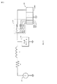
[0017] 図1は、DC電力供給装置110からアップストリーム回路115およびダウンストリーム回路120へ電力を分配するためのパワー分配ネットワーク(PDN:power distribution network)の例を示す。図1におけるインダクタLおよびレジスタRは、それぞれ、電力供給装置110と回路115および120との間のパッケージング相互接続(packaging interconnects)ならびに基板のインダクタンスおよび抵抗をモデル化(model)する。アップストリーム回路115およびダウンストリーム回路120は、同じダイ上に配置され得る。
FIG. 1 shows an example of a power distribution network (PDN) for distributing power from the DC
[0018] PDNは、電力を節約するためにパワーゲーティングを用い得る。この点で、PDNは、ダウンストリーム回路120を電力供給装置110に選択的に接続するための電力スイッチ130を含む。ダウンストリーム回路120がアクティブである時、電力スイッチ130は、ダウンストリーム回路120に電力を供給するためにオンにされ(turned on)、ダウンストリーム回路120が非アクティブである時、電力スイッチ130は、電力供給装置110をダウンストリーム回路120から切断するためにオフにされる(turned off)。これにより、ダウンストリーム回路120が非アクティブである時、ダウンストリーム回路120からの電力漏れが低減され、電力の節約になる。
[0018] The PDN may use power gating to save power. In this regard, the PDN includes a
[0019] ダウンストリーム回路120がアクティブである時、電力スイッチ130を通したIR電圧降下(voltage drop)を最小化するために、電力スイッチ130が非常に低い抵抗を有することが望ましい。しかしながら、これは、電力スイッチ130が最初に閉じられた時にアップストリーム回路115における供給電圧に大きな降下(droop)を招く可能性があり、アップストリーム回路115における論理に誤動作を生じさせる可能性がある。その大きな電圧降下は、ダウンストリーム回路120における複数のキャパシタによって引き起こされる。それらキャパシタは、ダウンストリーム回路120のトランジスタ中の寄生メタルラインキャパシタ(parasitic metal-line capacitors)および寄生キャパシタ(parasitic capacitors)を含み得る。ダウンストリーム回路120におけるそれらキャパシタは、ダウンストリーム回路120が非アクティブ状態から最初に覚醒される時、ほぼ全く電荷を有さない(have approximately no charge)。その結果、アップストリーム回路115およびダウンストリーム回路120が初めに電力スイッチ130によって接続される時、大量の電荷が、アップストリーム回路115におけるキャパシタからダウンストリーム回路120におけるキャパシタへ素早く流れ、アップストリーム回路115における供給電圧に降下を引き起こす。PDNは、PDNにおけるインダクタンスが原因で、電圧降下を防ぐのに十分な程速く電荷を供給することができない。
[0019] When the
[0020] 電圧降下のサイズは、以下の方程式によって近似され(be approximated)得る。

[0021] 方程式(1)から分かるように、電圧降下は、ダウンストリーム回路120のキャパシタンスがアップストリーム回路115のキャパシタンスと比較して大きい時、大きくなる可能性がある。例えば、CupとCdnとがおおよそ等しい時、Droopはおおよそ0.5(すなわち、供給電圧の50%)であり、それは大抵の場合には容認し難い程高い(unacceptably high)。
As can be seen from equation (1), the voltage drop can be large when the capacitance of the
[0022] 電圧降下を容認可能な限界内に保つための1つのアプローチは、ダウンストリーム回路120を複数のセクション(電力ドメイン)へ分割し、全体のダウンストリーム回路120を一度にパワーアップする代わりに、ダウンストリーム回路120のそれら複数のセクションを連続的にパワーアップすることである。この点で、図2は、ダウンストリーム回路120がN個の等しいサイズのセクション210(1)−210(N)へ分割され、電力スイッチ130がN個のスイッチ230(1)−230(N)を備える例を示す。各スイッチ230(1)−230(N)は、セクション210(1)−210(N)のうちのそれぞれ1つを電力供給装置110に選択的に接続するように構成される。これにより、ダウンストリーム回路120の各セクション210(1)−210(N)が別々にパワーアップされることが可能になる。
[0022] One approach to keeping the voltage drop within acceptable limits is to divide the
[0023] ダウンストリーム回路120が非アクティブの時、電力漏れを低減するために、スイッチ230(1)−230(N)は全て開かれる。ダウンストリーム回路120が非アクティブ状態から覚醒される(be awakened)ことになる時、スイッチ230(1)−230(N)は、ダウンストリーム回路120のセクション210(1)−210(N)を連続的にパワーアップするために連続的にオンにされる。第1のスイッチ230(1)は、時間t0においてオンにされ、第2のスイッチ230(2)は、時間t1においてオンにされ、第3のスイッチ230(3)は、時間t2においてオンにされ、N番目のスイッチ230(N)が時間t(N−1)においてオンにされるまで、そのように続く(and so forth)。隣接したスイッチ間の時間遅延は、複数のスイッチのうちの1つがオンにされる時、アップストリーム回路115が名目供給電圧(nominal supply voltage)に戻って落ち着く(settle back)のに十分な時間を取るまで次のスイッチがオンにされないように、選ばれ得る。
[0023] When the
[0024] このように、ダウンストリーム回路120が覚醒されることになる時、スイッチ230(1)−230(N)は、全体のダウンストリーム回路120を一度にパワーアップする代わりに、ダウンストリーム回路120のセクション210(1)−210(N)を連続的にパワーアップするために、連続的にオンにされる。各セクション210(1)−210(N)は、ダウンストリーム回路120のキャパシタンスのごく一部のみを有する。したがって、スイッチ230(1)−230(N)がオンにされる度に、充電される(charged up)必要があるのはダウンストリーム回路120のキャパシタンスのごく一部のみであり、これは格段により小さい電圧降下をもたらす。
[0024] Thus, when the
[0025] このアプローチの難点は、ダウンストリーム回路120のセクション210(1)−210(N)を連続的にパワーアップすることが、ダウンストリーム回路120の起動時間(wakeup time)を増加させることである。したがって、電圧降下制約条件内にまだ留まりながらもダウンストリーム回路の起動時間を低減するために、複数のセクションのサイズを最適化するための技法が望まれることになる。
[0025] The difficulty with this approach is that continuously powering up sections 210 (1) -210 (N) of
[0026] 以下にさらに説明されるように、本開示の実施形態は、電圧降下制約条件内にまだ留まりながらも起動時間を低減するために、ダウンストリーム回路のパワーゲーティングされた複数のセクションをサイジングするための技法を提供する。 [0026] As further described below, embodiments of the present disclosure sizing multiple power-gated sections of downstream circuitry to reduce start-up time while still remaining within voltage drop constraints Provide techniques for
[0027] 上の方程式(1)は、ダウンストリームキャパシタンスCdnを、アップストリームキャパシタンスCupおよびDroopの関数として(as a function of)表現するために、以下のように書き直され得る。
[0028] 方程式(2)は、ダウンストリーム回路120の各セクションに関するキャパシタンスを決定するために、以下のように、拡張されることができる。
[0029] 方程式(3)から分かるように、より多くのセクションがパワーアップされるにつれて、各セクションに関するキャパシタンスは漸進的に増加する。これは、方程式(3)におけるトータルのアップストリームキャパシタンス(すなわち、
[0030] 図3は、本開示の実施形態に従って、漸進的にサイズが大きくなる複数のセクション310(1)−310(M)へ分割されたダウンストリーム回路120を示す。上述したように、事実上の(effective)アップストリームキャパシタンスは、より多くのセクションがパワーアップされるにつれて増加するので、セクション310(1)−310(M)は漸進的にサイズが大きくなる。電力スイッチ130は、M個のスイッチ330(1)−330(M)を備え、ここで、各スイッチ330(1)−330(M)は、セクション310(1)−310(M)のうちのそれぞれ1つを電力供給装置110へ選択的に接続するように構成される。
[0030] FIG. 3 illustrates the
[0031] ダウンストリーム回路120が非アクティブ状態から覚醒されることになる時、スイッチ330(1)−330(M)は、サイズが大きくなっていく順番で(すなわち、最も小さいセクション310(1)から最も大きなセクション310(M)へと)、ダウンストリーム回路120のセクション310(1)−310(M)を連続的にパワーアップする。セクション310(1)−310(M)のサイズを漸進的に大きくすることは、等しいサイズの複数のセクションを使用することに比べて、パワーアップシーケンスの間にパワーアップされることが必要なセクションの数を低減し、したがって、ダウンストリーム回路120の起動時間を低減する。
[0031] When the
[0032] 方程式(3)は、本開示の実施形態に従って、ダウンストリーム回路120のパワーゲーティングされたセクション310(1)−310(M)のサイズを決定するための反復的なプロセスにおいて使用されることができる。第1の反復において、ダウンストリーム回路120の第1のセクション310(1)に関するキャパシタンスCdn(1)が、アップストリーム回路115のキャパシタンスCupと電圧降下制約条件とに基づいて、方程式(3)を使用して決定される。第1の反復について、方程式(3)は、前のセクションがないので、方程式(2)に等しい。電圧降下制約条件が0.05である例の場合、第1のセクション310(1)のキャパシタンスCdn(1)は、おおよそ0.05263*Cupである。第1のセクション310(1)のキャパシタンスCdn(1)が決定された後、第1のセクション310(1)のサイズは、第1のセクション310(1)のキャパシタンスCdn(1)を、ダウンストリーム回路120のキャパシタンス密度(単位面積当たりのキャパシタンス)で割ることによって、決定され得る。
[0032] Equation (3) is used in an iterative process to determine the size of the power-gated sections 310 (1) -310 (M) of the
[0033] 第2の反復において、ダウンストリーム回路120の第2のセクション310(2)に関するキャパシタンスCdn(2)は、アップストリーム回路115のキャパシタンスCupと、第1のセクション310(1)(前のセクション)のキャパシタンスCdn(1)と、電圧降下制約条件とに基づいて、方程式(3)を使用して決定される。電圧降下制約条件が0.05である例の場合、第2のセクション310(2)のキャパシタンスCdn(2)は、おおよそ0.0554*Cupである。したがって、第2のセクション310(2)のキャパシタンスCdn(2)は、第1のセクション310(1)のキャパシタンスCdn(1)よりも大きい。第2のセクション310(2)のキャパシタンスCdn(2)が決定された後、第2のセクション310(2)のサイズは、第2のセクション310(2)のキャパシタンスCdn(2)を、ダウンストリーム回路120のキャパシタンス密度で割ることによって、決定され得る。第2のセクション310(2)のキャパシタンスCdn(2)は、第1のセクション310(1)のキャパシタンスCdn(1)よりも大きいので、第2のセクション310(2)のサイズは、(比較的一様な(relatively uniform)キャパシタンス密度を想定すると)第1のセクション310(1)のサイズよりも大きい。
[0033] In the second iteration, the capacitance C dn (2) relates to the
[0034] 第3の反復では、ダウンストリーム回路120の第3のセクション310(3)に関するキャパシタンスCdn(3)は、アップストリーム回路115のキャパシタンスCupと、第1のおよび第2のセクション310(1)および310(2)(前のセクション)のキャパシタンスCdn(1)およびCdn(2)の合計と、電圧降下制約条件とに基づいて、方程式(3)を使用して決定される。電圧降下制約条件が0.05である例の場合、第3のセクションのキャパシタンスCdn(3)は、おおよそ0.0583*Cupである。したがって、第3のセクション310(3)のキャパシタンスCdn(3)は、第1のおよび第2のセクション310(1)および310(2)の各々のキャパシタンスよりも大きい。第3のセクション310(3)のキャパシタンスCdn(3)が決定された後、第3のセクション310(3)のサイズは、第3のセクション310(3)のキャパシタンスCdn(3)を、ダウンストリーム回路120のキャパシタンス密度で割ることによって、決定され得る。第3のセクション310(3)のキャパシタンスCdn(3)は、第1のおよび第2のセクション310(1)および310(2)の各々のキャパシタンスよりも大きいので、第3のセクション310(3)のサイズは、(比較的一様なキャパシタンス密度を想定すると)第1のおよび第2のセクション310(1)および310(2)の各々のサイズよりも大きい。
[0034] In the third iteration, the capacitance C dn (3) about the
[0035] 後続のセクション310(4)−310(M)のサイズは、追加的な反復を実行することにより決定され得、そこでは、各後続のセクションのキャパシタンスは、アップストリーム回路115のキャパシタンスCupと、前の複数のセクションのキャパシタンスの合計と、電圧降下制約条件とに基づいて、方程式(3)を使用して決定される。各後続のセクションのサイズは、その後続のセクションに関する決定されたキャパシタンスを、キャパシタンス密度で割ることによって決定される。前の複数のセクションのキャパシタンスの合計は各反復において増加するので、キャパシタンス(およびゆえにサイズ)は、各反復において増加する。
[0035] The size of subsequent sections 310 (4) -310 (M) may be determined by performing additional iterations, where the capacitance of each subsequent section is the capacitance C of
[0036] 反復的なプロセスは、複数のセクションのサイズの合計がダウンストリーム回路120の全エリアをカバーするまで続き得る。各反復は1つのセクションに対応するので、反復的なプロセスがストップする時、反復の数は、ダウンストリーム回路におけるセクション(電力ドメイン)の数に等しくなる。したがって、反復的なプロセスはまた、ダウンストリーム回路120が分割されることになるセクションの数(すなわち、M)を決定するためにも使用され得る。
[0036] The iterative process may continue until the sum of the sizes of the sections covers the entire area of the
[0037] 反復的なプロセスによって決定される複数のセクションのサイズの合計は、ダウンストリーム回路120のエリアよりも若干大きいことがあり得る。例えば、セクション310(1)−310(M−1)のサイズの合計がダウンストリーム回路120のエリアよりも若干小さいことがあり得る一方で、セクション310(1)−310(M)のサイズの合計がダウンストリーム回路120のエリアよりも若干大きいことがあり得る。この場合、セクション310(1)−310(M)のサイズは、セクション310(1)−310(M)のサイズの合計をダウンストリーム回路120のエリアにフィットさせるために、少量だけ比例的に(proportionally)低減され得る。
[0037] The sum of the sizes of the sections determined by an iterative process may be slightly larger than the area of the
[0038] 図4は、本開示の実施形態に従って、ダウンストリーム回路におけるパワーゲーティングされた複数のセクションをサイジングするための方法400を示す。
[0038] FIG. 4 illustrates a
[0039] ステップ410において、第1のセクションに関するキャパシタンスは、アップストリーム回路のキャパシタンスと電圧降下制約条件とに基づいて、決定される。例えば、第1のセクション(例えば、310(1))に関するキャパシタンス(例えば、Cdn(1))は、方程式(3)を使用して決定され得る。
[0039] In
[0040] ステップ420において、第2のセクションに関するキャパシタンスは、アップストリーム回路のキャパシタンスと、電圧降下制約条件と、第1のセクションに関する決定されたキャパシタンスとに基づいて、決定される。例えば、第2のセクション(例えば、310(2))に関するキャパシタンス(例えば、Cdn(2))は、方程式(3)を使用して決定され得、そこでは、方程式(3)における実効アップストリームキャパシタンス(effective upstream capacitance)は、アップストリーム回路(例えば、アップストリーム回路115)のキャパシタンスと第1のセクションに関するキャパシタンスとの合計である。
[0040] In
[0041] ステップ430において、第3のセクションに関するキャパシタンスは、アップストリーム回路のキャパシタンスと、電圧降下制約条件と、第1のおよび第2のセクションに関する決定されたキャパシタンスとに基づいて、決定される。例えば、第3のセクション(例えば、310(3))に関するキャパシタンス(例えば、Cdn(3))は、方程式(3)を使用して決定され得、そこでは、方程式(3)における実効アップストリームキャパシタンスは、アップストリーム回路(例えば、アップストリーム回路115)のキャパシタンスと第1のセクションおよび第2のセクションに関するキャパシタンスとの合計である。
[0041] At
[0042] ステップ440において、第1の、第2の、および第3のセクションの各々のサイズは、それらセクションの各々に関する決定されたキャパシタンスに基づいて、決定される。例えば、各セクションのサイズは、そのセクションに関する決定されたキャパシタンスを、ダウンストリーム回路のキャパシタンス密度で割ることによって、決定され得る。
[0042] In
[0043] 上述したように、電圧降下を決定するための方程式(1)は、スイッチが閉じられている時に有する抵抗がゼロ(すなわち、オン抵抗ゼロ)である理想的な電力スイッチを想定する。その結果、方程式(1)は、電力供給装置110からの電荷の寄与なく(with no charge contribution)スイッチが閉じられる時のアップストリーム回路115におけるキャパシタからダウンストリームキャパシタ120におけるキャパシタへの電荷の即座の転送(instantaneous transfer of charge)を電圧降下の原因と想定する。方程式(1)において電力供給装置110からの電荷の寄与がない理由は、PDNにおけるインダクタンスが、電力供給装置110が電荷をアップストリーム回路115に即座に供給することを防ぐからである。
[0043] As described above, equation (1) for determining the voltage drop assumes an ideal power switch that has zero resistance when the switch is closed (ie, zero on-resistance). As a result, equation (1) indicates that the instantaneous charge from the capacitor in the
[0044] 実際には、電力スイッチは、スイッチが閉じられる時、少量の抵抗を有し得る。スイッチの抵抗およびダウンストリーム回路120のキャパシタンスは、ある時間期間にわたってアップストリーム回路115からダウンストリーム回路120へ電荷が転送されることを引き起こすRC時定数(an RC time constant)を形成する。これは、電力供給装置110に、電圧降下を低減するためにアップストリーム回路115に電荷を供給するための時間を与える。その結果、実際の電圧降下は、方程式(1)で予測される電圧降下よりも小さい。
[0044] In practice, the power switch may have a small amount of resistance when the switch is closed. The resistance of the switch and the capacitance of the
[0045] それでも、方程式(1)によって予測される電圧降下は、スイッチの抵抗が低い時、実際の電圧降下の良好な近似値(good approximation)を提供する。これは、スイッチの抵抗が低い時、RC時定数は、電力供給装置110とアップストリーム回路115との間のPDNインダクタンス(例えば、基板およびパッケージングインダクタンス(packaging inductance))に関連する時定数よりも格段に小さいからである。その結果、アップストリーム回路115からダウンストリーム回路120への電荷の転送は、電力供給装置110からアップストリーム回路115への電荷の転送よりも格段に速く、その場合、方程式(1)によって予測される電圧降下は、実際の電圧降下に比較的近い。
[0045] Nevertheless, the voltage drop predicted by equation (1) provides a good approximation of the actual voltage drop when the switch resistance is low. This is because when the switch resistance is low, the RC time constant is greater than the time constant associated with the PDN inductance (eg, board and packaging inductance) between the
[0046] 上述したように、方程式(1)は、オン抵抗がゼロの(with zero on resistance)理想的なスイッチを想定しているので、方程式(1)を使用して決定される電圧降下は、実際の電圧降下よりも小さい。方程式(1)は、以下のように、電圧降下の式に補正係数(correction factor)を乗じることによって、スイッチの抵抗を考慮に入れるように修正され得る。
[0047] ダウンストリームキャパシタンスCdnを決定するための方程式(2)は、以下のように、方程式(4)に基づいて、修正され得る。
[0048] 図5は、本開示の実施形態に従って、パワーアップシーケンスの間の、アップストリーム回路115に関する電圧波形510、ならびにダウンストリーム回路120の第1の2つのセクション310(1)および310(2)に関する電圧波形520(1)および520(2)の例を示す。時間t0の前には、アップストリーム回路115の電圧は、電力供給装置110の供給電圧Vddにおおよそ等しい。また、時間t0の前には、ダウンストリーム回路120は、非アクティブであり、電力スイッチ130のスイッチ330(1)−330(M)の全ては、開かれている。その結果、第1のおよびセクションセクション310(1)および310(2)の各々の電圧は、おおよそゼロボルトである。
[0048] FIG. 5 illustrates a voltage waveform 510 for the
[0049] 時間t0において、第1のセクション310(1)に関するスイッチ330(1)は、第1のセクション310(1)をパワーアップするために閉じられる。これによって、電荷が、アップストリーム回路115におけるキャパシタからスイッチ330(1)を通して第1のセクション310(1)におけるキャパシタへと素早く流れる。電荷の転送は、アップストリーム回路115の電圧を素早く低減し、アップストリーム回路115における電圧降下515(1)をもたらす。低いオン抵抗を有するスイッチ(a switch having low on resistance)の場合、PDNのインダクタンスが電力供給装置110からアップストリーム回路115への転送電荷を遅くするので、電力供給装置110からの電荷は、電圧降下515(1)にそれほどの影響を与えない。電圧降下515(1)は、方程式(3)または(6)に従って第1のセクション310(1)をサイジングすることで、電圧降下制約条件(例えば、0.05)によって制限(bounded)され得る。図5に示される電圧降下515(1)のサイズは、説明し易さのために誇張されていることは理解されるべきである。
[0049] At time t0, the switch 330 (1) for the first section 310 (1) is closed to power up the first section 310 (1). This causes charge to flow quickly from the capacitor in the
[0050] 電圧降下515(1)の後、第1のセクション310(1)およびアップストリーム回路115の電圧が発振(oscillate)し、第1のセクション310(1)およびアップストリーム回路115においてパワーレールにおける電圧リップル(a voltage ripple)525(1)を生成する。この発振は、PDNのインダクタンス、第1のセクション310(1)およびアップストリーム回路115のキャパシタンス、並びに、PDN、アップストリーム回路115および第1のセクション310(1)の抵抗によって形成されるRLC回路の共振によって引き起こされる。共振は、第1のスイッチ330(1)を閉じることからもたらされる電圧降下515(1)によってトリガされる。RLC回路の共振周波数は、以下によって近似され得る。
[0051] 時間t0から時間遅延後、第2のセクション310(2)に関するスイッチ330(2)は、第2のセクション310(2)をパワーアップするために時間t1において閉じられる。1つの態様では、時間遅延は、第1のセクション310(1)およびアップストリーム回路115における電圧が、(整定時間(settling time)と称される)供給電圧Vddに近い値に落ち着くために十分な時間を提供する。例えば、整定時間は、リップル525(1)の電圧スイング(swing)が名目供給電圧の2パーセントより小さい値に減少するためにかかる時間であり得る。したがって、第2のセクション310(2)に関するスイッチ330(2)が閉じられる時間までに、アップストリーム回路115および第1のセクション310(1)は、おおよそ供給電圧Vddまで充電されている。
[0051] After a time delay from time t0, switch 330 (2) for second section 310 (2) is closed at time t1 to power up second section 310 (2). In one aspect, the time delay is sufficient for the voltage in the first section 310 (1) and the
[0052] 時間t1において、スイッチ330(2)は、第2のセクション310(2)をアップストリーム回路115および第1のセクション310(1)に接続し、これによって電荷が第1のセクション310(1)およびアップストリーム回路115におけるキャパシタから第2のセクション310(2)におけるキャパシタへと素早く流れる。電荷の転送は、第1のセクション310(1)およびアップストリーム回路115の電圧を素早く低減し、アップストリーム回路115および第1のセクション310(1)における電圧降下515(2)をもたらす。電圧降下515(2)は、方程式(3)または(6)に従って第2のセクション310(2)をサイジングすることで、電圧制約条件(例えば、0.05)によって制限され得る。図5に示される電圧降下515(2)のサイズは、説明し易さのために誇張されていることは理解されるべきである。
[0052] At time t1, the switch 330 (2) connects the second section 310 (2) to the
[0053] 電圧降下515(2)の後、第1のおよび第2のセクション310(1)および310(2)、ならびにアップストリーム回路115の電圧が発振し、パワーレールにおいて電圧リップル525(2)を生成する。リップル525(2)は、時間の経過と共に消滅し、第1のおよび第2のセクション310(1)および310(2)、ならびにアップストリーム回路115の電圧は、供給電圧Vddに近い値に落ち着く。
[0053] After voltage drop 515 (2), the voltage of first and second sections 310 (1) and 310 (2) and
[0054] 時間t1からの時間遅延の後、第3のセクション310(3)に関するスイッチ330(3)は、第3のセクション310(3)(図5に示されていない)をパワーアップするために閉じられる。時間遅延は、第3のセクション310(3)に関するスイッチ330(3)が閉じられる時間までに、アップストリーム回路115ならびに第1のおよび第2のセクション310(1)および310(2)がおおよそ供給電圧Vddまで充電されているように、リップル525(2)の整定時間におおよそ等しい可能性がある。
[0054] After a time delay from time t1, switch 330 (3) for third section 310 (3) powers up third section 310 (3) (not shown in FIG. 5). Closed. The time delay is approximately provided by the
[0055] 図6は、本開示の実施形態に従って、電力スイッチ130の例示的なインプリメンテーションを示す。この実施形態では、ダウンストリーム回路120のセクション310(1)−310(M)を連続的にパワーアップするためのスイッチ632(1)−632(M)は、複数のP型金属酸化膜半導体(PMOS)トランジスタスイッチを備える。各PMOSスイッチ632(1)−632(M)は、それぞれのゲートをハイ(high)に駆動することによって開かれ(オフにされ)得、それぞれのゲートをロー(low)に駆動することによって閉じられ(オンにされ)得る。図6は、各セクション310(1)−310(M)につき1つのPMOSスイッチ632(1)−632(M)を示しているが、電力スイッチ130は、各セクション310(1)−310(M)につき2つ以上のPMOSスイッチ632(1)−632(M)を備え得ることは理解されるべきである。例えば、電力スイッチ130は、各セクションに関して並列に接続された複数のPMOSスイッチを備え得る。
[0055] FIG. 6 illustrates an exemplary implementation of the
[0056] この実施形態では、スイッチ632(1)−632(M)は、電力管理デバイス640によって制御される。ダウンストリーム回路120が非アクティブ状態に入る場合、電力管理デバイス640は、電力漏れを低減するためにダウンストリーム回路120の各セクション310(1)−310(M)を、電力供給装置110から切断するために、スイッチ632(1)−632(M)の全てを開き得る。ダウンストリーム回路120が非アクティブ状態から覚醒される場合、電力管理デバイス640は、ダウンストリーム回路120のセクション310(1)−310(M)を連続的にパワーアップするために、パワーアップシーケンスの間にスイッチ632(1)−632(M)を連続的に閉じ(オンにし)得る。セクション310(1)−310(M)は、漸進的にサイズが大きくなり得、電力管理デバイス640は、セクション310(1)−310(M)がサイズが大きくなっていく順番で(すなわち、最も小さいセクション310(1)から最も大きなセクション310(M)へと)、パワーアップされるように、スイッチ632(1)−632(M)を連続的に閉じ(オンにし)得る。
[0056] In this embodiment, the switches 632 (1) -632 (M) are controlled by the
[0057] 電力管理デバイス640は、遅延チェーン652を形成するために直列に結合された複数の遅延素子650(1)−650(M−1)およびパワーゲートコントローラ645を備える。電力管理デバイス640の出力は、第1の遅延素子650(1)の入力および第1のスイッチ632(1)のゲートに結合される。遅延素子650(1)−650(M−1)の各々の出力は、スイッチ632(2)−632(M)のうちのそれぞれ1つのゲートに結合される。より具体的には、第1の遅延素子650(1)の出力は、第2のスイッチ632(2)のゲートに結合され、第2の遅延素子650(2)の出力は、第3のスイッチ632(3)のゲートに結合される、等(and so on)である。
[0057] The
[0058] ダウンストリーム回路120が非アクティブ状態から覚醒される場合、パワーゲートコントローラ645は、スイッチ632(1)−632(M)を連続的にオンにするために、時間t0において遅延チェーン652にパワーアップ信号を出力する。例えば、ダウンストリーム回路120は、アプリケーションまたは他の回路がダウンストリーム回路120を使用する必要がある時、覚醒され得る。スイッチ632(1)−632(M)がPMOSスイッチを使用してインプリメントされる時、PMOSスイッチのゲートをローに駆動することはPMOSスイッチをオンにするので、パワーアップ信号は、低電圧信号(論理ゼロ)を備え得る。
[0058] When the
[0059] 時間t0において、パワーアップ信号は、第1のセクション310(1)をパワーアップするために第1のスイッチ632(1)をオンにする。第1の遅延素子650(1)は、第1の時間遅延だけパワーアップ信号を遅延させ、時間t1において第2の遅延素子650(2)および第2のスイッチ632(2)へパワーアップ信号を出力する。したがって、第1の遅延素子650(1)の出力は、時間t0から第1の時間遅延後に、第2のスイッチ632(2)をオンにする。第1の時間遅延は、第1のセクション310(1)およびアップストリーム回路115における電圧のための整定時間におおよそ等しい可能性がある。
[0059] At time t0, the power up signal turns on the first switch 632 (1) to power up the first section 310 (1). The first delay element 650 (1) delays the power-up signal by a first time delay, and sends the power-up signal to the second delay element 650 (2) and the second switch 632 (2) at time t1. Output. Therefore, the output of the first delay element 650 (1) turns on the second switch 632 (2) after a first time delay from time t0. The first time delay may be approximately equal to the settling time for the voltage in the first section 310 (1) and the
[0060] 第2の遅延素子650(2)は、第2の時間遅延だけパワーアップ信号を遅延させ、時間t2において第3の遅延素子(図6に示されていない)および第3のスイッチ632(3)にパワーアップ信号を出力する。したがって、第2の遅延素子650(2)の出力は、第2の時間遅延の後、第3のスイッチ632(3)をオンにする。第2の時間遅延は、第1のおよび第2のセクション310(1)および310(2)、ならびにアップストリーム回路115における電圧のための整定時間におおよそ等しい可能性がある。
[0060] The second delay element 650 (2) delays the power-up signal by a second time delay, and a third delay element (not shown in FIG. 6) and a
[0061] 一般に、各遅延素子650(1)−650(M−1)は、その遅延素子の時間遅延だけパワーアップ信号を遅延させる。したがって、各遅延素子650(1)−650(M−1)の出力は、前のスイッチがオンにされた時間から時間遅延後に、それぞれのスイッチ632(2)−632(M)をオンにし、ここで、時間遅延は、その遅延素子の時間遅延におおよそ等しい。各遅延素子650(1)−650(M−1)の時間遅延は、前の複数のセクションおよびアップストリーム回路115における電圧のための整定時間におおよそ等しい可能性がある。
[0061] Generally, each delay element 650 (1) -650 (M-1) delays the power-up signal by the time delay of the delay element. Thus, the output of each delay element 650 (1) -650 (M-1) turns on the respective switch 632 (2) -632 (M) after a time delay from the time when the previous switch was turned on, Here, the time delay is approximately equal to the time delay of the delay element. The time delay of each delay element 650 (1) -650 (M-1) may be approximately equal to the settling time for the voltage in the previous sections and
[0062] 最後の遅延素子650(M−1)の出力は、パワーゲートコントローラ645に結合され得、その場合、パワーアップ信号は、遅延素子650(1)−650(M−1)を通して伝播した後、パワーゲートコントローラ645へ戻る。この実施形態では、パワーゲートコントローラ645は、パワーアップ信号の戻りを、ダウンストリーム回路120のセクション310(1)−310(M)がパワーアップされたことを示すインジケーションとして扱い得る。
[0062] The output of the last delay element 650 (M-1) may be coupled to a
[0063] 1つの実施形態では、ダウンストリーム回路120は、さまざまなサイズのパワーゲーティングされた複数のセクションへ分割されることができるメモリを備え得る。例えば、メモリは、多数のビット線を備え得、そこでは、各セクション310(1)−310(M)は、ビット線のサブセットを備える。この例では、各ビット線への電力は、別個のスイッチによって制御され得る。これは、回路設計者に、各セクションのビット線の数の選択について、ゆえに各セクションのサイズについて、柔軟性を提供する。セクションのビット線の数が多くなる程、そのセクションのサイズは大きくなる。
[0063] In one embodiment, the
[0064] 各セクションのサイズは、複数の異なるサイズから選択され得、ここで、各サイズは、異なる数のビット線に対応する。この例では、セクションのサイズが決定される時(例えば、方程式(3)または(6)に基づいて)、回路設計者は、複数のサイズから、そのセクションの決定されたサイズに最も近いサイズを選択し得る。最も近いサイズが、決定されたよりサイズよりも大きい場合には、回路設計者は、電圧降下制約条件が満たされることを保証するために、決定されたサイズより小さい、最も近いサイズを選択し得る。 [0064] The size of each section may be selected from a plurality of different sizes, where each size corresponds to a different number of bit lines. In this example, when the size of a section is determined (eg, based on equations (3) or (6)), the circuit designer can determine from the multiple sizes the size closest to the determined size of the section. You can choose. If the closest size is larger than the determined size, the circuit designer may select the closest size that is smaller than the determined size to ensure that the voltage drop constraint is met.
[0065] 図7は、本開示の実施形態に従って、漸進的にサイズが大きくなる複数のセクションを備える回路をパワーアップするための方法700を示す。
[0065] FIG. 7 illustrates a
[0066] ステップ710において、回路をパワーアップするための信号が受信される。例えば、信号は、パワーゲートコントローラ(例えば、パワーゲートコントローラ645)によって出力されたパワーアップ信号を備え得る。
[0066] In
[0067] ステップ720において、信号に応答して、複数のセクションは、サイズが大きくなっていく順番で、連続的にパワーアップされる。例えば、パワーアップ信号は、複数のセクション(例えば、310(1)−310(M))を電力供給装置(例えば、電力供給装置110)へ接続する複数のスイッチ(例えば、スイッチ632(1)−632(M))を、連続的にオンにする遅延チェーン(例えば、遅延チェーン625)を伝播(propagate down)し得る。
[0067] In
[0068] 本開示の先の説明は、当業者が本開示を製造するまたは使用することを可能にするために提供される。本開示への様々な修正は、当業者にとって容易に明らかであろうし、ここに定義された一般的な原理は、本開示の範囲または精神から逸脱することなく、他のバリエーションにも適用され得る。したがって、本開示は、ここに説明された例に限定されるようには意図されておらず、ここに開示された原理および新規な特徴と一致する最も広い範囲を与えられるべきである。
以下に、本願出願の当初の特許請求の範囲に記載された発明を付記する。
[C1]
ダウンストリーム回路におけるパワーゲーティングされた複数のセクションをサイジングするための方法であって、
アップストリーム回路のキャパシタンスと、電圧降下制約条件とに基づいて、第1のセクションに関するキャパシタンスを決定することと、
前記アップストリーム回路の前記キャパシタンスと、前記電圧降下制約条件と、前記第1のセクションに関する前記決定されたキャパシタンスとに基づいて、第2のセクションに関するキャパシタンスを決定することと、
前記アップストリーム回路の前記キャパシタンスと、前記電圧降下制約条件と、前記第1のおよび第2のセクションに関する前記決定されたキャパシタンスとに基づいて、第3のセクションに関するキャパシタンスを決定することと、
前記複数のセクションの各々に関する前記決定されたキャパシタンスに基づいて、前記第1の、第2の、および第3のセクションの各々のサイズを決定することと、
を備える、方法。
[C2]
前記ダウンストリーム回路は、メモリを備える、C1に記載の方法。
[C3]
前記第2のセクションに関する前記キャパシタンスを決定することは、前記アップストリーム回路の前記キャパシタンスと、前記第1のセクションに関する前記決定されたキャパシタンスとの合計に基づいて、前記第2のセクションに関する前記キャパシタンスを決定することを備える、C1に記載の方法。
[C4]
前記第3のセクションに関する前記キャパシタンスを決定することは、前記アップストリーム回路の前記キャパシタンスと、前記第1のセクションに関する前記決定されたキャパシタンスと、前記第2のセクションに関する前記決定されたキャパシタンスとの合計に基づいて、前記第3の第2のセクションに関する前記キャパシタンスを決定することを備える、C3に記載の方法。
[C5]
前記第1の、第2の、および第3のセクションの各々の前記サイズを決定することは、前記複数のセクションの各々に関する前記決定されたキャパシタンスを、キャパシタンス密度で割ることを備える、C1に記載の方法。
[C6]
前記第1のセクションに関する前記キャパシタンスを決定することは、補正係数に基づいて、前記第1のセクションに関する前記キャパシタンスを決定することを備える、C1に記載の方法。
[C7]
前記補正係数は少なくとも0.8の値を有する、C6に記載の方法。
[C8]
前記電圧降下制約条件は、おおよそ0.05またはそれより小さい、C1に記載の方法。
[C9]
漸進的にサイズが大きくなる複数のセクションを備える回路をパワーアップするための方法であって、
前記回路をパワーアップするための信号を受信することと、
前記信号に応答して、サイズが大きくなっていく順番で、前記複数のセクションを連続的にパワーアップすることと、
を備える、方法。
[C10]
前記複数のセクションは異なるキャパシタンスを有し、前記複数のセクションを連続的にパワーアップすることは、キャパシタンスが増えていく順番で前記複数のセクションを連続的にパワーアップすることを備える、C9に記載の方法。
[C11]
前記回路は、前記複数のセクションに分割されたメモリを備える、C9に記載の方法。
[C12]
前記複数のセクションの各々は、別個のスイッチによってパワーレールに選択的に接続され、前記複数のセクションを連続的にパワーアップすることは、前記複数のスイッチを連続的に閉じることを備える、C9に記載の方法。
[C13]
前記複数のスイッチを連続的に閉じることは、
前記複数のセクションのうちの第1の1つに関する前記スイッチを閉じることと、
時間遅延の後に、前記複数のセクションのうちの第2の1つに関する前記スイッチを閉じることと、ここにおいて、前記時間遅延は、前記複数のセクションのうちの前記第1の1つに関する前記スイッチを前記閉じることによってトリガされる前記パワーレールにおける電圧リップルの整定時間と等しいかまたはそれより長い、
を備える、C12に記載の方法。
[C14]
漸進的にサイズが大きくなる複数のセクションを備える回路をパワーアップするための装置であって、
前記回路をパワーアップするための信号を受信するための手段と、
前記信号に応答して、サイズが大きくなっていく順番で、前記複数のセクションを連続的にパワーアップするための手段と、
を備える、装置。
[C15]
前記複数のセクションは異なるキャパシタンスを有し、前記複数のセクションを連続的にパワーアップするための前記手段は、キャパシタンスが増えていく順番で前記複数のセクションを連続的にパワーアップするための手段を備える、C14に記載の装置。
[C16]
前記回路は、前記複数のセクションに分割されたメモリを備える、C14に記載の装置。
[C17]
前記複数のセクションの各々は、別個のスイッチによってパワーレールに選択的に接続され、および前記複数のセクションを連続的にパワーアップするための前記手段は、前記複数のスイッチを連続的に閉じるための手段を備える、C14に記載の装置。
[C18]
前記複数のスイッチを連続的に閉じるための前記手段は、
前記複数のセクションのうちの第1の1つに関する前記スイッチを閉じるための手段と、
時間遅延の後に、前記複数のセクションのうちの第2の1つに関する前記スイッチを閉じるための手段と、ここにおいて、前記時間遅延は、前記複数のセクションのうちの前記第1の1つに関する前記スイッチを前記閉じることによってトリガされる前記パワーレールにおける電圧リップルの整定時間と等しいかまたはそれより長い、
を備える、C17に記載の装置。
[C19]
漸進的にサイズが大きくなる複数のセクションを備える回路をパワーアップするための装置であって、
複数のスイッチと、ここにおいて、前記複数のスイッチの各々は、前記複数のセクションのうちのそれぞれ1つをパワーレールに選択的に接続するように構成される、
前記複数のスイッチが、サイズが大きくなっていく順番で前記複数のセクションを連続的にパワーアップするように、前記複数のスイッチを連続的に閉じるように構成される、電力管理デバイスと、
を備える、装置。
[C20]
前記複数のセクションは異なるキャパシタンスを有し、前記電力管理デバイスは、前記複数のスイッチが、キャパシタンスが増えていく順番で前記複数のセクションを連続的にパワーアップするように、前記複数のスイッチを連続的に閉じるように構成される、C19に記載の装置。
[C21]
前記回路は、前記複数のセクションに分割されたメモリを備える、C19に記載の装置。
[C22]
前記電力管理デバイスは、
遅延チェーンを形成するために直列に結合された複数の遅延素子と、各スイッチは、前記遅延チェーンに沿った異なるポイントに結合される、
前記回路が非アクティブ状態からパワーアップされることになる場合、パワーアップ信号を前記遅延チェーンへ出力するように構成されるパワーゲートコントローラと、
を備える、C19に記載の装置。
[C23]
前記複数のスイッチの各々は、1つ以上のP型金属酸化膜半導体(PMOS)トランジスタを備え、前記パワーアップ信号は低電圧信号である、C22に記載の装置。
[C24]
前記遅延素子のうちの1つの時間遅延は、前記複数のスイッチのうちの1つを閉じることによってトリガされる前記パワーレールにおける電圧リップルの整定時間と等しいかまたはそれより長い、C23に記載の装置。
[0068] The previous description of the disclosure is provided to enable any person skilled in the art to make or use the disclosure. Various modifications to this disclosure will be readily apparent to those skilled in the art and the generic principles defined herein may be applied to other variations without departing from the scope or spirit of this disclosure. . Accordingly, this disclosure is not intended to be limited to the examples described herein but is to be accorded the widest scope consistent with the principles and novel features disclosed herein.
Hereinafter, the invention described in the scope of claims of the present application will be appended.
[C1]
A method for sizing multiple power-gated sections in a downstream circuit comprising:
Determining the capacitance for the first section based on the capacitance of the upstream circuit and the voltage drop constraint;
Determining a capacitance for a second section based on the capacitance of the upstream circuit, the voltage drop constraint, and the determined capacitance for the first section;
Determining a capacitance for a third section based on the capacitance of the upstream circuit, the voltage drop constraint, and the determined capacitance for the first and second sections;
Determining the size of each of the first, second, and third sections based on the determined capacitance for each of the plurality of sections;
A method comprising:
[C2]
The method of C1, wherein the downstream circuit comprises a memory.
[C3]
Determining the capacitance with respect to the second section may include determining the capacitance with respect to the second section based on a sum of the capacitance of the upstream circuit and the determined capacitance with respect to the first section. The method of C1, comprising determining.
[C4]
Determining the capacitance for the third section is the sum of the capacitance of the upstream circuit, the determined capacitance for the first section, and the determined capacitance for the second section. The method of C3, comprising determining the capacitance for the third second section based on.
[C5]
C1, wherein determining the size of each of the first, second, and third sections comprises dividing the determined capacitance for each of the plurality of sections by a capacitance density. the method of.
[C6]
The method of C1, wherein determining the capacitance for the first section comprises determining the capacitance for the first section based on a correction factor.
[C7]
The method of C6, wherein the correction factor has a value of at least 0.8.
[C8]
The method of C1, wherein the voltage drop constraint is approximately 0.05 or less.
[C9]
A method for powering up a circuit comprising multiple sections of progressively increasing size, comprising:
Receiving a signal to power up the circuit;
Continually powering up the plurality of sections in order of increasing size in response to the signal;
A method comprising:
[C10]
The plurality of sections have different capacitances, and sequentially powering up the plurality of sections comprises sequentially powering up the plurality of sections in order of increasing capacitance. the method of.
[C11]
The method of C9, wherein the circuit comprises a memory divided into the plurality of sections.
[C12]
Each of the plurality of sections is selectively connected to a power rail by a separate switch, and continuously powering up the plurality of sections comprises sequentially closing the plurality of switches to C9 The method described.
[C13]
Continuously closing the plurality of switches includes
Closing the switch for a first one of the plurality of sections;
Closing the switch for a second one of the plurality of sections after a time delay, wherein the time delay turns on the switch for the first one of the plurality of sections. Equal to or longer than the settling time of the voltage ripple in the power rail triggered by the closing,
The method of C12, comprising:
[C14]
An apparatus for powering up a circuit comprising a plurality of sections of progressively increasing size,
Means for receiving a signal for powering up the circuit;
Means for continuously powering up the plurality of sections in order of increasing size in response to the signal;
An apparatus comprising:
[C15]
The plurality of sections have different capacitances, and the means for sequentially powering up the plurality of sections comprises means for continuously powering up the plurality of sections in order of increasing capacitance. The apparatus of C14, comprising.
[C16]
The apparatus of C14, wherein the circuit comprises a memory divided into the plurality of sections.
[C17]
Each of the plurality of sections is selectively connected to a power rail by a separate switch, and the means for continuously powering up the plurality of sections is for continuously closing the plurality of switches. The apparatus of C14, comprising means.
[C18]
The means for sequentially closing the plurality of switches comprises:
Means for closing the switch for a first one of the plurality of sections;
Means for closing the switch for a second one of the plurality of sections after a time delay, wherein the time delay is for the first one of the plurality of sections; Equal to or longer than the settling time of the voltage ripple in the power rail triggered by the closing of the switch,
The apparatus according to C17, comprising:
[C19]
An apparatus for powering up a circuit comprising a plurality of sections of progressively increasing size,
A plurality of switches, wherein each of the plurality of switches is configured to selectively connect a respective one of the plurality of sections to a power rail;
A power management device configured to sequentially close the plurality of switches such that the plurality of switches continuously power up the plurality of sections in order of increasing size;
An apparatus comprising:
[C20]
The plurality of sections have different capacitances, and the power management device continuously switches the plurality of switches such that the plurality of switches continuously power up the plurality of sections in order of increasing capacitance. The device of C19, wherein the device is configured to automatically close.
[C21]
The apparatus of C19, wherein the circuit comprises a memory divided into the plurality of sections.
[C22]
The power management device is
A plurality of delay elements coupled in series to form a delay chain, and each switch is coupled to a different point along the delay chain;
A power gate controller configured to output a power up signal to the delay chain if the circuit is to be powered up from an inactive state;
The apparatus according to C19, comprising:
[C23]
The apparatus according to C22, wherein each of the plurality of switches comprises one or more P-type metal oxide semiconductor (PMOS) transistors, and the power-up signal is a low voltage signal.
[C24]
The apparatus of C23, wherein a time delay of one of the delay elements is equal to or longer than a settling time of a voltage ripple in the power rail triggered by closing one of the plurality of switches. .
Claims (10)
アップストリーム回路の供給端子間で定義される前記アップストリーム回路に対応するキャパシタンスと、電圧降下制約条件とに基づいて、第1のセクションに関する供給端子間で定義される前記ダウンストリーム回路に対応するキャパシタンスを決定することと、
前記アップストリーム回路の前記キャパシタンスと、前記電圧降下制約条件と、前記第1のセクションに関する前記決定されたキャパシタンスとに基づいて、第2のセクションに関する供給端子間で定義される前記ダウンストリーム回路に対応するキャパシタンスを決定することと、
前記アップストリーム回路の前記キャパシタンスと、前記電圧降下制約条件と、前記第1のおよび第2のセクションに関する前記決定されたキャパシタンスとに基づいて、第3のセクションに関する供給端子間で定義される前記ダウンストリーム回路に対応するキャパシタンスを決定することと、
前記複数のセクションの各々に関する前記決定されたキャパシタンスに基づいて、前記第1の、第2の、および第3のセクションの各々のサイズを決定することと、
を備える、方法。 A method for sizing multiple power-gated sections in a downstream circuit comprising:
And the capacitance corresponding to the upstream circuit defined between the supply terminals of the upstream circuit, on the basis of the voltage drop constraints, the capacitance corresponding to the downstream circuit defined between the supply terminal for the first section And determining
Corresponding to the downstream circuit defined between the supply terminals for the second section based on the capacitance of the upstream circuit, the voltage drop constraint, and the determined capacitance for the first section Determining the capacitance to be
The down defined between supply terminals for a third section based on the capacitance of the upstream circuit, the voltage drop constraint, and the determined capacitance for the first and second sections. Determining the capacitance corresponding to the stream circuit;
Determining the size of each of the first, second, and third sections based on the determined capacitance for each of the plurality of sections;
A method comprising:
アップストリーム回路の供給端子間で定義される前記アップストリーム回路に対応するキャパシタンスと、電圧降下制約条件とに基づいて、第1のセクションに関する供給端子間で定義される前記ダウンストリーム回路に対応するキャパシタンスを決定するための手段と、
前記アップストリーム回路の前記キャパシタンスと、前記電圧降下制約条件と、前記第1のセクションに関する前記決定されたキャパシタンスとに基づいて、第2のセクションに関する供給端子間で定義される前記ダウンストリーム回路に対応するキャパシタンスを決定するための手段と、
前記アップストリーム回路の前記キャパシタンスと、前記電圧降下制約条件と、前記第1のおよび第2のセクションに関する前記決定されたキャパシタンスとに基づいて、第3のセクションに関する供給端子間で定義される前記ダウンストリーム回路に対応するキャパシタンスを決定するための手段と、
前記複数のセクションの各々に関する前記決定されたキャパシタンスに基づいて、前記第1の、第2の、および第3のセクションの各々のサイズを決定するための手段と、
を備える、装置。 An apparatus for sizing multiple power-gated sections in a downstream circuit,
And the capacitance corresponding to the upstream circuit defined between the supply terminals of the upstream circuit, on the basis of the voltage drop constraints, the capacitance corresponding to the downstream circuit defined between the supply terminal for the first section Means for determining
Corresponding to the downstream circuit defined between the supply terminals for the second section based on the capacitance of the upstream circuit, the voltage drop constraint, and the determined capacitance for the first section Means for determining the capacitance to be
The down defined between supply terminals for a third section based on the capacitance of the upstream circuit, the voltage drop constraint, and the determined capacitance for the first and second sections. Means for determining a capacitance corresponding to the stream circuit;
Means for determining a size of each of the first, second, and third sections based on the determined capacitance for each of the plurality of sections;
An apparatus comprising:
Applications Claiming Priority (3)
| Application Number | Priority Date | Filing Date | Title |
|---|---|---|---|
| US14/157,503 US9367054B2 (en) | 2014-01-16 | 2014-01-16 | Sizing power-gated sections by constraining voltage droop |
| US14/157,503 | 2014-01-16 | ||
| PCT/US2015/011762 WO2015109188A1 (en) | 2014-01-16 | 2015-01-16 | Sizing power-gated sections by constraining voltage droop |
Publications (3)
| Publication Number | Publication Date |
|---|---|
| JP2017509202A JP2017509202A (en) | 2017-03-30 |
| JP2017509202A5 JP2017509202A5 (en) | 2018-02-08 |
| JP6556736B2 true JP6556736B2 (en) | 2019-08-07 |
Family
ID=52446439
Family Applications (1)
| Application Number | Title | Priority Date | Filing Date |
|---|---|---|---|
| JP2016546760A Active JP6556736B2 (en) | 2014-01-16 | 2015-01-16 | Sizing multiple sections gated by constraining the voltage drop |
Country Status (7)
| Country | Link |
|---|---|
| US (1) | US9367054B2 (en) |
| EP (1) | EP3095193A1 (en) |
| JP (1) | JP6556736B2 (en) |
| KR (1) | KR102219822B1 (en) |
| CN (1) | CN105917583B (en) |
| BR (1) | BR112016016431A2 (en) |
| WO (1) | WO2015109188A1 (en) |
Families Citing this family (4)
| Publication number | Priority date | Publication date | Assignee | Title |
|---|---|---|---|---|
| KR102184740B1 (en) * | 2014-06-16 | 2020-11-30 | 에스케이하이닉스 주식회사 | Electronic device and electronic system with the same |
| US9438244B2 (en) * | 2014-10-28 | 2016-09-06 | Xilinx, Inc. | Circuits for and methods of controlling power within an integrated circuit |
| US10152112B2 (en) * | 2015-06-10 | 2018-12-11 | Sonics, Inc. | Power manager with a power switch arbitrator |
| US10928886B2 (en) | 2019-02-25 | 2021-02-23 | Intel Corporation | Frequency overshoot and voltage droop mitigation apparatus and method |
Family Cites Families (15)
| Publication number | Priority date | Publication date | Assignee | Title |
|---|---|---|---|---|
| JP2797761B2 (en) * | 1991-07-11 | 1998-09-17 | 日本電気株式会社 | Power-on circuit |
| AU7706198A (en) | 1997-05-30 | 1998-12-30 | Micron Technology, Inc. | 256 meg dynamic random access memory |
| KR100780750B1 (en) | 2006-05-11 | 2007-11-30 | 한국과학기술원 | Power Network Using Standard Cell and Power Gating Cell, and Semiconductor Device Using a Power Network |
| JP2008065732A (en) | 2006-09-11 | 2008-03-21 | Nec Electronics Corp | Design method and design system for semiconductor integrated circuit |
| US20080120514A1 (en) * | 2006-11-10 | 2008-05-22 | Yehea Ismail | Thermal management of on-chip caches through power density minimization |
| US7868479B2 (en) * | 2007-06-27 | 2011-01-11 | Qualcomm Incorporated | Power gating for multimedia processing power management |
| US8958575B2 (en) * | 2007-06-29 | 2015-02-17 | Qualcomm Incorporated | Amplifier with configurable DC-coupled or AC-coupled output |
| JP5326628B2 (en) | 2008-03-03 | 2013-10-30 | 富士通株式会社 | Electronic circuit equipment |
| US8302059B2 (en) | 2008-05-27 | 2012-10-30 | Nxp B.V. | Power switch design method and program |
| EP2369509A1 (en) | 2010-03-01 | 2011-09-28 | Nxp B.V. | Method of generating an integrated circuit layout and integrated circuit |
| US8266569B2 (en) | 2010-03-05 | 2012-09-11 | Advanced Micro Devices, Inc. | Identification of critical enables using MEA and WAA metrics |
| JP2011199094A (en) * | 2010-03-23 | 2011-10-06 | Renesas Electronics Corp | Semiconductor integrated circuit and method of controlling power switch of the semiconductor integrated circuit |
| WO2011137339A2 (en) | 2010-04-30 | 2011-11-03 | Cornell University | Systems and methods for zero-delay wakeup for power gated asynchronous pipelines |
| WO2012012291A2 (en) * | 2010-07-19 | 2012-01-26 | National Semiconductor Corporation | Adaptive signal equalizer with segmented coarse and fine controls |
| JP6100076B2 (en) * | 2012-05-02 | 2017-03-22 | 株式会社半導体エネルギー研究所 | Processor |
-
2014
- 2014-01-16 US US14/157,503 patent/US9367054B2/en active Active
-
2015
- 2015-01-16 EP EP15702610.5A patent/EP3095193A1/en not_active Withdrawn
- 2015-01-16 WO PCT/US2015/011762 patent/WO2015109188A1/en active Application Filing
- 2015-01-16 KR KR1020167021743A patent/KR102219822B1/en active IP Right Grant
- 2015-01-16 CN CN201580004789.0A patent/CN105917583B/en not_active Expired - Fee Related
- 2015-01-16 JP JP2016546760A patent/JP6556736B2/en active Active
- 2015-01-16 BR BR112016016431A patent/BR112016016431A2/en not_active IP Right Cessation
Also Published As
| Publication number | Publication date |
|---|---|
| JP2017509202A (en) | 2017-03-30 |
| WO2015109188A1 (en) | 2015-07-23 |
| BR112016016431A2 (en) | 2017-08-08 |
| KR20160108433A (en) | 2016-09-19 |
| US20150198933A1 (en) | 2015-07-16 |
| EP3095193A1 (en) | 2016-11-23 |
| US9367054B2 (en) | 2016-06-14 |
| CN105917583A (en) | 2016-08-31 |
| CN105917583B (en) | 2021-05-07 |
| KR102219822B1 (en) | 2021-02-23 |
Similar Documents
| Publication | Publication Date | Title |
|---|---|---|
| US10651733B2 (en) | Bridge driver for a switching voltage regulator which is operable to soft-switch and hard-switch | |
| TWI691824B (en) | Electric power conversion device and method for estimating current | |
| JP6556736B2 (en) | Sizing multiple sections gated by constraining the voltage drop | |
| TW201904180A (en) | Soft-charging of switched capacitors in power converter circuits | |
| US20070279100A1 (en) | Recycling Charge to Reduce Energy Consumption During Mode Transition in Muiltithreshold Complementary Metal-Oxide-Semiconductor (MTCMOS) Circuits | |
| KR102022355B1 (en) | Power Gating Circuit of System On Chip | |
| JP2009147934A (en) | Sizing and arrangement of charge recycling (cr) of multi-threshold cmos (mtcmos) circuit | |
| CN106462174B (en) | To minimize the method and apparatus of switching noise interference | |
| JP2009147933A (en) | Charge recycling of power gated cmos circuit and super cutoff cmos circuit | |
| US20140167868A1 (en) | Power-efficient multi-frequency resonant clock meshes | |
| JP6553057B2 (en) | Voltage-dependent die RC modeling for system-level power distribution networks | |
| US11128281B2 (en) | Reduced-power electronic circuits with wide-band energy recovery using non-interfering topologies | |
| US20140184295A1 (en) | Controlled resonant power transfer | |
| US7705626B2 (en) | Design structure to eliminate step response power supply perturbation | |
| JP2009064921A (en) | Semiconductor device and power compensation method | |
| Bezzam et al. | An energy-recovering reconfigurable series resonant clocking scheme for wide frequency operation | |
| WO2009067470A2 (en) | Charge recycling a 1 of n ndl gate with a time varying power supply | |
| Meshkat et al. | A fully integrated soft switched high frequency resonant DC‐DC voltage regulator | |
| Xu et al. | Decoupling capacitance design strategies for power delivery networks with power gating | |
| Sathe | Quasi-resonant clocking: A run-time control approach for true voltage-frequency-scalability | |
| US11038413B2 (en) | Power converter with overshoot compensation for a switching device | |
| JP2011199113A (en) | Analyzer and semiconductor device | |
| Sheikhaei et al. | Energy recycling from multigigahertz clocks using fully integrated switching converters | |
| CN103701451A (en) | Input-driven domino circuit design | |
| Anusha et al. | MTCMOS DESIGN FOR EFFECTIVE VOLTAGE DROP CONTROL |
Legal Events
| Date | Code | Title | Description |
|---|---|---|---|
| A521 | Request for written amendment filed |
Free format text: JAPANESE INTERMEDIATE CODE: A523 Effective date: 20171221 |
|
| A621 | Written request for application examination |
Free format text: JAPANESE INTERMEDIATE CODE: A621 Effective date: 20171221 |
|
| A131 | Notification of reasons for refusal |
Free format text: JAPANESE INTERMEDIATE CODE: A131 Effective date: 20181204 |
|
| A977 | Report on retrieval |
Free format text: JAPANESE INTERMEDIATE CODE: A971007 Effective date: 20181130 |
|
| A521 | Request for written amendment filed |
Free format text: JAPANESE INTERMEDIATE CODE: A523 Effective date: 20190122 |
|
| TRDD | Decision of grant or rejection written | ||
| A01 | Written decision to grant a patent or to grant a registration (utility model) |
Free format text: JAPANESE INTERMEDIATE CODE: A01 Effective date: 20190611 |
|
| A61 | First payment of annual fees (during grant procedure) |
Free format text: JAPANESE INTERMEDIATE CODE: A61 Effective date: 20190710 |
|
| R150 | Certificate of patent or registration of utility model |
Ref document number: 6556736 Country of ref document: JP Free format text: JAPANESE INTERMEDIATE CODE: R150 |
|
| R250 | Receipt of annual fees |
Free format text: JAPANESE INTERMEDIATE CODE: R250 |
|
| R250 | Receipt of annual fees |
Free format text: JAPANESE INTERMEDIATE CODE: R250 |