JP6552410B2 - Fast fabrication of devices with individually patterned anisotropy - Google Patents
Fast fabrication of devices with individually patterned anisotropy Download PDFInfo
- Publication number
- JP6552410B2 JP6552410B2 JP2015514406A JP2015514406A JP6552410B2 JP 6552410 B2 JP6552410 B2 JP 6552410B2 JP 2015514406 A JP2015514406 A JP 2015514406A JP 2015514406 A JP2015514406 A JP 2015514406A JP 6552410 B2 JP6552410 B2 JP 6552410B2
- Authority
- JP
- Japan
- Prior art keywords
- light
- slm
- substrate
- polarization
- layer
- Prior art date
- Legal status (The legal status is an assumption and is not a legal conclusion. Google has not performed a legal analysis and makes no representation as to the accuracy of the status listed.)
- Active
Links
Images


Classifications
-
- G—PHYSICS
- G03—PHOTOGRAPHY; CINEMATOGRAPHY; ANALOGOUS TECHNIQUES USING WAVES OTHER THAN OPTICAL WAVES; ELECTROGRAPHY; HOLOGRAPHY
- G03F—PHOTOMECHANICAL PRODUCTION OF TEXTURED OR PATTERNED SURFACES, e.g. FOR PRINTING, FOR PROCESSING OF SEMICONDUCTOR DEVICES; MATERIALS THEREFOR; ORIGINALS THEREFOR; APPARATUS SPECIALLY ADAPTED THEREFOR
- G03F7/00—Photomechanical, e.g. photolithographic, production of textured or patterned surfaces, e.g. printing surfaces; Materials therefor, e.g. comprising photoresists; Apparatus specially adapted therefor
- G03F7/70—Microphotolithographic exposure; Apparatus therefor
- G03F7/70058—Mask illumination systems
- G03F7/70191—Optical correction elements, filters or phase plates for controlling intensity, wavelength, polarisation, phase or the like
-
- G—PHYSICS
- G02—OPTICS
- G02B—OPTICAL ELEMENTS, SYSTEMS OR APPARATUS
- G02B5/00—Optical elements other than lenses
- G02B5/30—Polarising elements
- G02B5/3025—Polarisers, i.e. arrangements capable of producing a definite output polarisation state from an unpolarised input state
-
- B—PERFORMING OPERATIONS; TRANSPORTING
- B29—WORKING OF PLASTICS; WORKING OF SUBSTANCES IN A PLASTIC STATE IN GENERAL
- B29D—PRODUCING PARTICULAR ARTICLES FROM PLASTICS OR FROM SUBSTANCES IN A PLASTIC STATE
- B29D11/00—Producing optical elements, e.g. lenses or prisms
- B29D11/00634—Production of filters
- B29D11/00644—Production of filters polarizing
-
- B—PERFORMING OPERATIONS; TRANSPORTING
- B42—BOOKBINDING; ALBUMS; FILES; SPECIAL PRINTED MATTER
- B42D—BOOKS; BOOK COVERS; LOOSE LEAVES; PRINTED MATTER CHARACTERISED BY IDENTIFICATION OR SECURITY FEATURES; PRINTED MATTER OF SPECIAL FORMAT OR STYLE NOT OTHERWISE PROVIDED FOR; DEVICES FOR USE THEREWITH AND NOT OTHERWISE PROVIDED FOR; MOVABLE-STRIP WRITING OR READING APPARATUS
- B42D25/00—Information-bearing cards or sheet-like structures characterised by identification or security features; Manufacture thereof
- B42D25/30—Identification or security features, e.g. for preventing forgery
- B42D25/36—Identification or security features, e.g. for preventing forgery comprising special materials
- B42D25/364—Liquid crystals
-
- G—PHYSICS
- G02—OPTICS
- G02B—OPTICAL ELEMENTS, SYSTEMS OR APPARATUS
- G02B27/00—Optical systems or apparatus not provided for by any of the groups G02B1/00 - G02B26/00, G02B30/00
- G02B27/28—Optical systems or apparatus not provided for by any of the groups G02B1/00 - G02B26/00, G02B30/00 for polarising
- G02B27/286—Optical systems or apparatus not provided for by any of the groups G02B1/00 - G02B26/00, G02B30/00 for polarising for controlling or changing the state of polarisation, e.g. transforming one polarisation state into another
-
- G—PHYSICS
- G02—OPTICS
- G02B—OPTICAL ELEMENTS, SYSTEMS OR APPARATUS
- G02B5/00—Optical elements other than lenses
- G02B5/30—Polarising elements
- G02B5/3083—Birefringent or phase retarding elements
-
- G—PHYSICS
- G03—PHOTOGRAPHY; CINEMATOGRAPHY; ANALOGOUS TECHNIQUES USING WAVES OTHER THAN OPTICAL WAVES; ELECTROGRAPHY; HOLOGRAPHY
- G03F—PHOTOMECHANICAL PRODUCTION OF TEXTURED OR PATTERNED SURFACES, e.g. FOR PRINTING, FOR PROCESSING OF SEMICONDUCTOR DEVICES; MATERIALS THEREFOR; ORIGINALS THEREFOR; APPARATUS SPECIALLY ADAPTED THEREFOR
- G03F1/00—Originals for photomechanical production of textured or patterned surfaces, e.g., masks, photo-masks, reticles; Mask blanks or pellicles therefor; Containers specially adapted therefor; Preparation thereof
-
- G—PHYSICS
- G02—OPTICS
- G02F—OPTICAL DEVICES OR ARRANGEMENTS FOR THE CONTROL OF LIGHT BY MODIFICATION OF THE OPTICAL PROPERTIES OF THE MEDIA OF THE ELEMENTS INVOLVED THEREIN; NON-LINEAR OPTICS; FREQUENCY-CHANGING OF LIGHT; OPTICAL LOGIC ELEMENTS; OPTICAL ANALOGUE/DIGITAL CONVERTERS
- G02F1/00—Devices or arrangements for the control of the intensity, colour, phase, polarisation or direction of light arriving from an independent light source, e.g. switching, gating or modulating; Non-linear optics
- G02F1/01—Devices or arrangements for the control of the intensity, colour, phase, polarisation or direction of light arriving from an independent light source, e.g. switching, gating or modulating; Non-linear optics for the control of the intensity, phase, polarisation or colour
- G02F1/13—Devices or arrangements for the control of the intensity, colour, phase, polarisation or direction of light arriving from an independent light source, e.g. switching, gating or modulating; Non-linear optics for the control of the intensity, phase, polarisation or colour based on liquid crystals, e.g. single liquid crystal display cells
- G02F1/1303—Apparatus specially adapted to the manufacture of LCDs
-
- G—PHYSICS
- G02—OPTICS
- G02F—OPTICAL DEVICES OR ARRANGEMENTS FOR THE CONTROL OF LIGHT BY MODIFICATION OF THE OPTICAL PROPERTIES OF THE MEDIA OF THE ELEMENTS INVOLVED THEREIN; NON-LINEAR OPTICS; FREQUENCY-CHANGING OF LIGHT; OPTICAL LOGIC ELEMENTS; OPTICAL ANALOGUE/DIGITAL CONVERTERS
- G02F2203/00—Function characteristic
- G02F2203/12—Function characteristic spatial light modulator
Description
分野
本発明は、個別にパターン化された異方性を有する素子を高速に製造するための方法、及び、装置に関する。
FIELD The present invention relates to a method and apparatus for high speed manufacturing of individually patterned elements having anisotropy.
背景
パターン化された異方性(anisotropic properties)を有する素子は、例えば、光学素子として公知であり、光学素子は、局所的に異なる光学軸方向を有し、重合、又は、架橋した液晶を含んだ層を含む。このような層は、例えば、局所的に異なるアライメント方向を呈するアライメント層上に架橋性液晶材料を適用することによって調製される。液晶材料は、基底アライメント層の局所的なアライメント方向を取り入れ、次いで、配向を固定するために架橋させられる。
Background Elements with patterned anisotropic properties are known, for example, as optical elements, which have locally different optical axis directions and contain polymerized or crosslinked liquid crystals. Including layers. Such a layer is prepared, for example, by applying a crosslinkable liquid crystal material on an alignment layer that exhibits locally different alignment directions. The liquid crystal material incorporates the local alignment direction of the underlying alignment layer and is then crosslinked to fix the alignment.
局所的に異なるアライメント方向を有するアライメント層は、光の偏光に感度を有する材料の層が直線偏光光に暴露される場合に、光配向技術によって容易に調製され得る。パターン化されたアライメントは、光配向層の異なる領域の暴露のために光の偏光方向を変化させることによって、達成される。例えば、米国特許第7,375,888号では、このアライメントが、続く暴露工程では異なるフォトマスクで光配向層の一部を覆うことによって、実行される。 Alignment layers having locally different alignment directions can be readily prepared by photo-alignment techniques when a layer of material that is sensitive to the polarization of light is exposed to linearly polarized light. Patterned alignment is achieved by changing the polarization direction of the light for exposure of different areas of the photoalignment layer. For example, in US Pat. No. 7,375,888, this alignment is performed by covering a portion of the photoalignment layer with a different photomask in a subsequent exposure step.
先に記載した光学素子などの、個別にパターン化された異方性を有する素子は、それぞれの情報を有する別個のフォトマスクを使用することによって、上記の方法で原則的に製造され得る。しかしながら、このような方法は、大量に製造するにはほとんど適用不可能である。 Elements with individually patterned anisotropy, such as the optical elements described above, can in principle be manufactured in the above manner by using separate photomasks with the respective information. However, such methods are hardly applicable for mass production.
概要
本発明の目的は、パターンが素子毎に変化し得る場合に、個別にパターン化された異方性を有する素子を製造することを可能にする装置を提供することである。本発明の別の目的は、このような素子を高速に製造するための方法を提供することである。
Overview The object of the present invention is to provide a device which makes it possible to produce devices with individually patterned anisotropy, if the pattern can vary from device to device. Another object of the present invention is to provide a method for manufacturing such devices at high speed.
異方性は、例えば、光吸収、複屈折、導電性、分子配向、他の材料、例えば液晶のアライメントの特性、又は、弾性率などの機械的特性であってもよい。本出願の関連では、「アライメント方向」という用語は、異方性の対称軸を指す。 The anisotropy may be, for example, light absorption, birefringence, conductivity, molecular orientation, other materials such as alignment characteristics of liquid crystals, or mechanical characteristics such as elastic modulus. In the context of the present application, the term "alignment direction" refers to an anisotropic symmetry axis.
本出願の関連では、光配向可能材料は、光の偏光に感度を有し、適した波長の偏光光への暴露の際に異方性が誘導され得る材料である。加えて、光配向された材料という用語は、アライニング光への暴露によってアラインされた光配向可能材料(photo-alignable material)を指すために使用される。 In the context of this application, a photoalignable material is a material that is sensitive to the polarization of light and whose anisotropy can be induced upon exposure to polarized light of a suitable wavelength. In addition, the term photo-aligned material is used to refer to a photo-alignable material that is aligned by exposure to aligning light.
光配向可能材料で誘導される異方性は、光配向可能材料と接触する従材料(slave material)へ更に伝達されてもよい。結果として、従材料もまた、異方性を呈することができる。従材料は、偏光光へ暴露される前に、光配向可能材料と混合されてもよく、又は、光配向された材料の表面と接触させられてもよい。 The anisotropy induced in the photoalignable material may be further transmitted to a slave material in contact with the photoalignable material. As a result, the slave material can also exhibit anisotropy. The slave material may be mixed with the photoalignable material before being exposed to polarized light, or may be brought into contact with the surface of the photoaligned material.
本出願の関連では、「従材料」は、光配向された材料との接触の際に異方性を確立する能力を有した任意の材料を指す。光配向された材料の、及び、従材料の異方性の性質は、互いに異なってもよい。例えば、従材料は、可視光に対する光吸収異方性を呈してもよく、したがって偏光子としての機能を果たすことができるが、光配向された材料の異方性は、分子配向に関するだけであってもよい。アライニング光に感度を有しないが、アライニング光への暴露の際に光反応する感光部分との相互作用のために異方性を創出する光配向可能材料の一部分、例えばコポリマー、が同様に存在してもよい。このような材料は、光配向可能材料の、及び、従材料の特性を呈するが、光配向可能材料の意味に包含される。 In the context of the present application, "secondary material" refers to any material that has the ability to establish anisotropy upon contact with a photo-oriented material. The anisotropic nature of the photo-oriented material and the slave material may be different from each other. For example, the secondary material may exhibit light absorption anisotropy to visible light and thus can function as a polarizer, but the anisotropy of the photo-oriented material is only related to molecular orientation May be A portion of a photoalignable material, such as a copolymer, that is not sensitive to aligning light but that also creates anisotropy due to interaction with the photosensitive moiety that is photoreactive upon exposure to aligning light It may exist. Such materials exhibit the properties of photoalignable materials and secondary materials, but are included within the meaning of photoalignable materials.
従材料は、重合性(polymerizable)、及び/又は、非重合性(non-polymerizable)化合物を含んでもよい。本出願の関連において、「重合性(polymerizable)」、及び、「重合した(polymerized)」という用語は、それぞれ「架橋性(cross-linkable)」、及び、「架橋した(cross-linked)」の意味を包含する。同様に、「重合(polymerization)」は「架橋(cross-linking)」の意味を包含する。 The secondary material may comprise a polymerizable and / or non-polymerizable compound. In the context of the present application, the terms "polymerizable" and "polymerized" refer to "cross-linkable" and "cross-linked" respectively Include the meaning. Similarly, "polymerization" includes the meaning of "cross-linking".
好ましくは、従材料は自己組織化材料(self organizing material)である。従材料は液晶材料(liquid crystal material)であることがより好ましく、従材料は液晶ポリマー材料(liquid crystal polymer material)であることが特に好ましい。 Preferably, the slave material is a self organizing material. The secondary material is more preferably a liquid crystal material, and the secondary material is particularly preferably a liquid crystal polymer material.
本出願の関連において使用されるような液晶ポリマー(LCP:liquid crystal polymer)材料は、液晶モノマー、及び/又は、液晶オリゴマー、及び/又は、液晶ポリマー、及び/又は、架橋した液晶を含む液晶材料を意味する。液晶材料が液晶モノマーを含む場合には、このようなモノマーは、典型的に、異方性が光配向された材料との接触によりLCP材料に創出された後に、重合してもよい。重合は、熱処理によって、又は、好ましくはuv(紫外線)−光を含む、化学線光(actinic light)に対する暴露によって、開始され得る。LCP−材料は、単一のタイプの液晶化合物からなってもよいが、異なる重合性、及び/又は、非重合性化合物の組成物であってもよく、化合物のすべてが液晶化合物でなければならないというわけではない。更に、LCP材料は、例えば光開始剤、又は、等方性若しくは異方性蛍光、及び/若しくは、非蛍光染料などの、添加剤を含有してもよい。 A liquid crystal polymer (LCP) material as used in the context of this application is a liquid crystal material comprising liquid crystal monomers and / or liquid crystal oligomers and / or liquid crystal polymers and / or cross-linked liquid crystals. Means Where the liquid crystal material includes a liquid crystal monomer, such a monomer may typically be polymerized after anisotropy has been created in the LCP material by contact with the photoaligned material. The polymerization can be initiated by heat treatment or by exposure to actinic light, preferably including uv (ultraviolet) light. The LCP-material may consist of a single type of liquid crystal compound, but may be a composition of different polymerizable and / or non-polymerizable compounds, all of the compounds must be liquid crystal compounds Not that. Furthermore, the LCP material may contain additives, such as, for example, photoinitiators, or isotropic or anisotropic fluorescent and / or non-fluorescent dyes.
本出願の関連では、光配向可能材料を含む層はまた、偏光光に既に暴露されたかどうかにかかわらず、光制御分子配向(LCMO:light controlled molecular orientation)層と称される。したがって、本明細書で使用されるようなLCMO層は、偏光光に暴露されない間は異方性を有しなくてもよく、偏光光に暴露された後に異方性を有する。典型的に、LCMO層は、基板に適用された薄層であり得る。LCMO層が厚く、機械的に十分安定していることも可能であり、結果として、LCMO層が追加的な基板なしで取り扱われ得る。LCMO層が厚い場合には、LCMO層はまた、基板の機能を有する。 In the context of the present application, the layer comprising the photoalignable material is also referred to as a light controlled molecular orientation (LCMO) layer, whether or not it has already been exposed to polarized light. Thus, an LCMO layer as used herein may have no anisotropy while not being exposed to polarized light, and has an anisotropy after being exposed to polarized light. Typically, the LCMO layer can be a thin layer applied to a substrate. It is also possible that the LCMO layer is thick and mechanically stable enough so that the LCMO layer can be handled without additional substrate. If the LCMO layer is thick, the LCMO layer also has the function of a substrate.
本出願の関連では、「アライニング光」という用語は、光配向可能材料に異方性を誘導することができ、少なくとも部分的に直線、又は、楕円偏光される光を意味する。好ましくは、アライニング光は、5:1を超える偏光度で直線偏光される。アライニング光の波長、強度、及び、エネルギーは、光配向可能材料の感光性に応じて選択される。典型的に、波長は、UV−A、UV−B、及び/若しくは、UV−C領域内、又は、可視領域内にある。好ましくは、アライニング光は、450nm未満の波長の光を含む。アライニング光が420nm未満の波長の光を含むことがより好ましい。 In the context of the present application, the term "aligning light" means light which can induce anisotropy in the photoalignable material and is at least partially linearly or elliptically polarized. Preferably, the aligning light is linearly polarized with a degree of polarization greater than 5: 1. The wavelength, intensity and energy of the aligning light are selected according to the photosensitivity of the photoalignable material. Typically, the wavelength is in the UV-A, UV-B, and / or UV-C region, or in the visible region. Preferably, the aligning light includes light having a wavelength of less than 450 nm. More preferably, the aligning light includes light having a wavelength of less than 420 nm.
アライニング光が直線偏光される場合には、アライニング光の偏光面は、アライニング光の伝搬方向、及び、偏光方向によって画定される面を意味する。アライニング光が楕円偏光される場合には、偏光面は、光の伝搬方向によって、及び、偏光楕円の長軸によって画定される面を意味する。 When the aligning light is linearly polarized, the polarization plane of the aligning light means a plane defined by the propagation direction of the aligning light and the polarization direction. When the aligning light is elliptically polarized, the plane of polarization means the plane defined by the propagation direction of the light and by the major axis of the polarization ellipse.
本発明の第1の態様によれば、個別にパターン化された異方性を有する素子を製造するための装置が提供される。装置は、
− 基板のための支持体と、
− 第1の偏光面(polarization plane)を有する空間変調(spatially modulated)されたアライニング光(aligning light)を提供する露光ユニットと、を備え、露光ユニットは、
− 光源と、
− 空間光変調器(spatial light modulator)であって、例えばコンピュータによって、電子的に制御が可能である空間光変調器と、
− 投影レンズと、を収容する。
According to a first aspect of the invention, there is provided an apparatus for manufacturing individually patterned elements having anisotropy. The device
-A support for the substrate;
An exposure unit for providing spatially modulated aligning light having a first polarization plane, the exposure unit comprising:
-A light source;
-A spatial light modulator, which can be controlled electronically, for example by a computer;
A projection lens;
このような装置は、フォトマスクを使用することなくパターン化された異方性を生成するために、LCMO層の照射のための空間変調されたアライニング光の異なるパターンを順次に提供することを可能にする。空間光変調器が電子的に制御が可能であるので、空間変調されたアライニング光の異なるパターンを素早く提供することが可能であり、したがって、個別にパターン化された情報を有する素子の高速、及び、自動的な製造が実行可能となる。 Such an apparatus provides sequentially providing different patterns of spatially modulated aligning light for illumination of the LCMO layer in order to generate patterned anisotropy without using a photomask. to enable. Since the spatial light modulator is electronically controllable, it is possible to quickly provide different patterns of spatially modulated aligning light, and thus high speeds of elements with individually patterned information, And, automatic manufacture becomes feasible.
好ましくは、基板のための支持体は、基板を、段階的に若しくは継続的に、又は、その両方で、移動させることができる。支持体は、例えば、バッチ処理のための基板の単片のために設計されてもよく、又は、例えばリールからリールまで、連続的な処理のために可撓性基板を移送してもよい。連続的な処理のための装置は、バッファシステムを備えてもよく、バッファシステムは、装置の他の部分では基板が移動したまま、露光ユニットの位置で基板の移動を局所的に停止することを可能にする。 Preferably, the support for the substrate is capable of moving the substrate stepwise or continuously or both. The support may be designed, for example, for a single piece of substrate for batch processing, or may transfer a flexible substrate for continuous processing, eg, from reel to reel. The apparatus for continuous processing may comprise a buffer system that stops the movement of the substrate locally at the position of the exposure unit while the substrate is moving in other parts of the apparatus. to enable.
基板面という用語は、基板が露光ユニットの空間変調されたアライニング光に暴露されることになる位置での、基板の上表面を組み込む面を指すために、本出願の関連では使用される。基板は装置の一部ではないので、基板面は、所望の基板が照射されることになる状況のための仮想面である。 The term substrate surface is used in the context of the present application to refer to the surface incorporating the upper surface of the substrate at the position where the substrate is to be exposed to the spatially modulated aligning light of the exposure unit. Because the substrate is not part of the device, the substrate surface is a virtual surface for the situation where the desired substrate is to be illuminated.
本出願の関連では、光の空間変調は、光強度の変調を指す。 In the context of this application, spatial modulation of light refers to modulation of light intensity.
任意の種類の空間光変調器(SLM:spatially light modulator)が、アライニング光を空間変調するために使用され得る。好ましくは、SLMは、liquid crystal on silicon(LCOS)ディスプレイなどの、透過型液晶ディスプレイ(LCD)若しくは反射型LCD、デジタルミラーデバイス(DMD)、又は、有機発光ダイオード(OLED)ディスプレイである。 Any type of spatial light modulator (SLM) may be used to spatially modulate the aligning light. Preferably, the SLM is a transmissive liquid crystal display (LCD) or reflective LCD, such as a liquid crystal on silicon (LCOS) display, a digital mirror device (DMD), or an organic light emitting diode (OLED) display.
本出願で使用されるようなSLMは、空間変調された光の生成のために必要とされる任意の光学、又は、電気的手段を備える。例えば、LCD、又は、LCOS−ディスプレイがSLMとして使用される場合には、SLMはまた、所望の強度変調を生成するために、到来する光を偏光して、透過、又は、反射光をそれぞれ分析するための適切な偏光子を含む。 SLMs as used in the present application comprise any optical or electrical means required for the generation of spatially modulated light. For example, if an LCD or LCOS-display is used as the SLM, then the SLM also polarizes the incoming light and analyzes the transmitted or reflected light respectively to produce the desired intensity modulation. To include appropriate polarizers.
「SLM光」という用語は、SLMによって空間変調された、所望の投射方向に沿って伝搬する光を意味する。換言すると、SLM光は、光配向可能材料の照射のために所望される光だけを包含する。例えば、DMDのマイクロミラーからアブソーバまで屈折される光は、「SLM光」の意味に包含されない。 The term “SLM light” means light that is spatially modulated by the SLM and propagates along the desired projection direction. In other words, the SLM light contains only the light desired for the illumination of the photoalignable material. For example, light refracted from a DMD micromirror to an absorber is not included in the meaning of “SLM light”.
光の偏光は、光源と照射される基板の位置との間の光路上の任意の点で実行され得る。偏光光のための手段、又は、光の偏光状態を変化させる手段は、光源と空間光変調器との間、及び/又は、空間光変調器と基板との間の任意の場所に位置決定され得る。光源が偏光光を発することもまた可能である。 Polarization of light may be performed at any point on the light path between the light source and the position of the substrate to be illuminated. The means for polarized light or the means for changing the polarization state of the light is located anywhere between the light source and the spatial light modulator and / or between the spatial light modulator and the substrate. obtain. It is also possible for the light source to emit polarized light.
原則的に、光源の物理的寸法が露光ユニットの光学系と両立できるようにされる限り、所望の波長領域の光を提供する任意のタイプの光源が使用可能である。好ましくは、光源は、高圧若しくは超高圧水銀ランプ、又は、発光ダイオード(LED)である。空間光変調器が、自発光であってもよく、有機発光ダイオード(OLED)に基づいてもよい。この場合、光源は、空間光変調器の一部であるとみなされる。好ましくは、光源は、450nm未満の波長の光を発する。光源が350nm〜420nmの波長領域の光を発することがより好ましい。 In principle, any type of light source providing light in the desired wavelength range can be used as long as the physical dimensions of the light source are made compatible with the optics of the exposure unit. Preferably, the light source is a high pressure or ultra high pressure mercury lamp or a light emitting diode (LED). The spatial light modulator may be self-luminous or based on an organic light emitting diode (OLED). In this case, the light source is considered to be part of the spatial light modulator. Preferably, the light source emits light of wavelength less than 450 nm. More preferably, the light source emits light in a wavelength region of 350 nm to 420 nm.
好ましくは、SLMは、市販のデジタルディスプレイ、又は、プロジェクタで使用されるユニットなどの、アドレス可能ユニットのマトリックスを有する。これらのユニットは、ピクセルとして一般に公知である。しかしながら、本発明によるSLMは、マトリックスタイプのSLMに限定されず、SLMは任意の形状、及び、配置のアドレス可能ユニットを含んでもよい。「ピクセル」という用語は、本出願の関連では、形状、又は、配置とは無関係に、これらのアドレス可能ユニットを指すために、総称的に使用される。 Preferably, the SLM has a matrix of addressable units, such as commercially available digital displays or units used in projectors. These units are commonly known as pixels. However, SLMs according to the present invention are not limited to matrix type SLMs, and SLMs may include addressable units of any shape and arrangement. The term "pixel" is used generically in the context of the present application to refer to these addressable units, regardless of shape or arrangement.
本出願の関連では、「SLM露光ユニット」という用語は、空間変調されたアライニング光を提供することができ、光源、投影レンズ、及び、空間光変調器を収容する露光ユニットを意味する。 In the context of the present application, the term "SLM exposure unit" means an exposure unit capable of providing spatially modulated aligning light and containing a light source, a projection lens and a spatial light modulator.
SLM露光ユニットは、光源、SLM、投影レンズ、及び、偏光手段などの、構成部品が共通のハウジングに位置する構成に制限されない。それよりもむしろ、構成部品が、物理的に分離され、SLM露光ユニットの機能を共に提供するように配置されてもよい。例えば、光源、及び、SLMがハウジングに配置され、偏光子が、ハウジングの外側にあり、例えば、基板面の近くに位置決定される場合であっても、アライニング光の偏光を提供する偏光子はSLM露光ユニットの一部とみなされる。 The SLM exposure unit is not limited to an arrangement in which the components are located in a common housing, such as the light source, the SLM, the projection lens and the polarization means. Rather, the components may be physically separated and arranged to provide the functionality of the SLM exposure unit together. For example, a polarizer that provides polarization of aligning light even when the light source and the SLM are disposed in the housing and the polarizer is outside the housing and is positioned near the substrate surface, for example. Are considered as part of the SLM exposure unit.
好ましい実施形態では、装置は、第2の偏光面を有するアライニング光を提供する手段を備える。第2の偏光面を有するアライニング光は、同様にSLM露光ユニットであってもよい追加的な偏光源によって提供されてもよく、及び/又は、SLM露光ユニットが、第1の、及び、第2の偏光面を有するアライニング光を提供することができる。 In a preferred embodiment, the device comprises means for providing aligning light having a second polarization plane. Aligning light having a second polarization plane may be provided by an additional polarization source, which may also be a SLM exposure unit, and / or the SLM exposure unit comprises a first and a second Aligning light having two polarization planes can be provided.
本発明による装置は、LCMO層、及び/又は、好ましくはLCP−材料である従材料の層を適用するコーティング、又は、印刷ユニットを更に備えてもよい。理想的には、装置は、LCMO層を適用する1つと、好ましくはLCP材料である従材料を適用するもう1つの、2つのコーティング、又は、印刷ユニットを備える。 The device according to the invention may further comprise a coating or printing unit applying a layer of LCMO and / or a secondary material, preferably a LCP-material. Ideally, the apparatus comprises two coating or printing units, one applying an LCMO layer and another applying a slave material, preferably an LCP material.
本発明による装置は、基板を持ち上げ異なる処理ステージへ搬送する基板取扱システムを更に備えてもよい。 The apparatus according to the invention may further comprise a substrate handling system for lifting the substrate and transporting it to a different processing stage.
好ましくは、本発明による装置は、基板、及び、基板上のコーティングの温度を上昇させる加熱ステージを備える。 Preferably, the apparatus according to the invention comprises a substrate and a heating stage for raising the temperature of the coating on the substrate.
装置は、例えば従材料の、重合反応を開始するための化学線光を提供する光源を更に収容する。 The apparatus further contains a light source, for example a secondary material, providing actinic light for initiating the polymerization reaction.
本発明の第2の態様によれば、個別にパターン化された異方性を有する光学素子を高速に製造するための方法が提供される。方法は、
− LCMO層を準備する工程と、
− LCMO層をSLM露光ユニットの空間変調されたアライニング光に暴露する工程であって、光の空間変調が電子的に制御された空間光変調器によって生成される工程と、を含む。
According to a second aspect of the present invention, there is provided a method for rapidly producing an optical element having individually patterned anisotropy. The method is
-Preparing a LCMO layer;
Exposing the LCMO layer to the spatially modulated aligning light of the SLM exposure unit, wherein the spatial modulation of the light is generated by an electronically controlled spatial light modulator.
好ましくは、光配向可能材料は、300〜450nmの波長領域の光に感度を有し、より好ましくは350〜420nmの波長領域、最も好ましくは380〜410nmの領域の光に感度を有する。 Preferably, the photoalignable material is sensitive to light in the wavelength region of 300-450 nm, more preferably sensitive to light in the wavelength region of 350-420 nm, most preferably 380-410 nm.
本発明の好ましい方法では、LCMO層は、異方性が光配向可能材料との接触によって創出され得る従材料を含む。好ましくは、従材料はLCP材料である。アライニング光への暴露の間、及び/又は、後にLCMO層を加熱することは、従材料の異方性を創出する助けとなる。任意に、方法はまた、熱処理、又は、化学線光への暴露によって従材料の重合を開始する工程を含む。 In a preferred method of the invention, the LCMO layer comprises a secondary material whose anisotropy can be created by contact with a photoalignable material. Preferably, the secondary material is an LCP material. Heating the LCMO layer during and / or after the exposure to the aligning light helps to create the anisotropy of the secondary material. Optionally, the method also includes the step of initiating polymerization of the slave material by heat treatment or exposure to actinic light.
本発明の別の好ましい方法では、従材料が、照射されたLCMO層上に適用される。好ましくは、従材料はLCP材料である。従材料の層の加熱は、従材料の異方性を創出する助けとなる。任意に、方法はまた、熱処理、又は、化学線光への暴露によって従材料の重合を開始する工程を含む。 In another preferred method of the invention, a slave material is applied over the irradiated LCMO layer. Preferably, the secondary material is an LCP material. The heating of the layer of the secondary material helps to create the anisotropy of the secondary material. Optionally, the method also comprises the step of initiating the polymerization of the secondary material by heat treatment or exposure to actinic light.
対応するSLM光がそれぞれのピクセルの最大強度を有するようにSLMのピクセルのすべてが切り替えられる場合に、基板の表面に投射されるアライニング光の強度の空間分布が均一でないことがあり得る。これは、例えば、光源の、又は、投射光学系の幾何学的形状によって引き起こされ得る。強度分布を均一にするために、SLMのそれぞれのピクセルからの放射が、最大放射と比較して低減されてもよい。不均一を補償するためにSLMにアドレスすることにより光学設定、及び、光の空間変調によって引き起こされる空間強度変化は、本発明の意味における光の変調とみなされない。したがって、それぞれのピクセルに対して、動作中に使用されている最大、及び、最小強度レベルにそれぞれ対応するオン状態、及び、オフ状態が定められる。それゆえ、オン状態は100%の光強度と定義されるが、例えば較正による、最大可能光強度に対応しない。 If all of the SLM pixels are switched so that the corresponding SLM light has the maximum intensity of each pixel, the spatial distribution of the intensity of the aligning light projected onto the surface of the substrate may not be uniform. This can be caused, for example, by the geometry of the light source or of the projection optics. The radiation from each pixel of the SLM may be reduced as compared to the maximum radiation in order to make the intensity distribution uniform. Optical settings by addressing the SLM to compensate for non-uniformity and spatial intensity changes caused by spatial modulation of the light are not considered as modulation of the light within the meaning of the invention. Thus, for each pixel, an on state and an off state are defined that correspond to the maximum and minimum intensity levels being used during operation, respectively. Therefore, the on-state is defined as 100% light intensity, but does not correspond to the maximum possible light intensity, eg by calibration.
本出願の関連では、「投影エリア」という表現は、SLMのピクセルのすべてがオン状態であるようにアドレスされるときにSLM露光ユニットの焦点面に照明されるエリアである。 In the context of this application, the expression “projection area” is the area that is illuminated on the focal plane of the SLM exposure unit when all of the pixels of the SLM are addressed to be on.
本発明が、添付図面によって更に示される。様々な特徴が必ずしも尺度通りに描かれていないことを強調しておく。 The invention is further illustrated by the attached drawings. It is emphasized that the various features are not necessarily drawn to scale.
発明の詳細な説明
本発明による方法、及び、装置は、空間変調されたアライニング光をLCMO層の表面上に投射することによって、個別にパターン化された異方性を有する素子の高速な製造を可能にする。
DETAILED DESCRIPTION OF THE INVENTION The method and apparatus according to the present invention is a rapid fabrication of individually patterned elements with anisotropy by projecting spatially modulated aligning light onto the surface of the LCMO layer. Enable.
本発明の一態様によれば、基板のための支持体、第1の偏光面を有する空間変調されたアライニング光を提供する空間光変調器を備えた露光ユニットを備える装置が提供される。露光ユニットは、例えば、光源、投影レンズ、及び、コンピュータによって電子的に制御が可能である空間光変調器を備える。 According to one aspect of the present invention, there is provided an apparatus comprising: a support for a substrate, an exposure unit comprising a spatial light modulator for providing spatially modulated aligning light having a first polarization plane. The exposure unit includes, for example, a light source, a projection lens, and a spatial light modulator that can be electronically controlled by a computer.
本出願の関連では基板のための支持体は、基板を担持、取扱、又は、搬送することができる任意の機械部品であり得る。例えば、支持体は単純な基板ホルダであり得、基板ホルダ上に、1つ以上の基板が、バッチプロセスにおけるSLM露光ユニットの空間変調されたアライニング光への基板の暴露のために、設置され得る。支持体はまた、装置の異なる処理ステージへ移動することができる可動式基板ホルダであってもよい。支持体の高度な変形例、例えばロボットアームは、好ましくは、例えばコンピュータによって電子的に制御されて、基板を追加的に持ち上げることができ、異なる処理ステージへ基板を移動させることができる。用語支持体はまた、リールツーリール製造設備などの継続的な製造装置の、リールなどの基板搬送システムを含む。 In the context of the present application, the support for the substrate may be any mechanical part capable of carrying, handling or transporting the substrate. For example, the support can be a simple substrate holder on which one or more substrates are placed for exposure of the substrate to the spatially modulated aligning light of the SLM exposure unit in a batch process. obtain. The support may also be a movable substrate holder that can be moved to different processing stages of the apparatus. Advanced variations of the support, such as a robotic arm, are preferably electronically controlled, for example by a computer, which can additionally lift the substrate and move the substrate to a different processing stage. The term support also includes substrate transport systems, such as reels, of continuous manufacturing equipment, such as reel-to-reel manufacturing equipment.
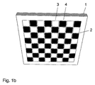
図1aは、マトリックス状に配置されるピクセル2を有したSLM1を示す。図1aのピクセルはオフ状態である。オフ状態は、対応するSLM光強度が最も低いことを意味し、対応してすべてのピクセルが黒で描かれる。
FIG. 1a shows an
図1bでは、SLM1のピクセル2はチェック模様画像を表示するようにアドレスされ、ピクセル3はオン状態に切り替えられ、ピクセル4はオフ状態である。
In FIG. 1b,
一般に、ピクセルは、任意の形態を有することができ、マトリックス状に配置される必要はない。図1a、及び、図1bのSLMは、任意のタイプのSLMを表す。図1a、及び、図1bのSLMは、例えば、liquid crystal on silicon(LCOS)ディスプレイなどの透過型、又は、反射型LCD、DMD、又は、OLEDディスプレイであり得る。簡潔に示すため、SLMのピクセルだけが示され、電気回路、又は、偏光素子などの、SLMの他の部分は示されない。偏光素子は、偏光光を提供するため、及び、偏光状態の空間的変化を光強度の空間的変化に変換するために、LCD−SLMの場合には必要とされる。 In general, the pixels can have any form and need not be arranged in a matrix. The SLMs of FIGS. 1a and 1b represent any type of SLM. The SLM of FIGS. 1a and 1b can be, for example, a transmissive or reflective LCD, DMD, or OLED display such as a liquid crystal on silicon (LCOS) display. For the sake of simplicity, only the pixels of the SLM are shown, and other parts of the SLM, such as electrical circuits or polarization elements, are not shown. A polarizing element is required in the case of LCD-SLMs to provide polarized light and to convert the spatial change in polarization state into a spatial change in light intensity.
光源から発せられる光の偏光を生じさせるために、ワイヤグリッド偏光子、プリズム偏光子、ブリュースタータイプ偏光子、多層干渉偏光子、又は、染料タイプ若しくはヨウ素系シート偏光子のような吸収偏光子などの、所望の波長領域に好適な任意のタイプの偏光子が使用可能である。光源自体が偏光光を発してもよく、結果として、SLMのタイプに応じて、追加的な偏光子が必要とされなくてもよい。 Wire grid polarizers, prism polarizers, Brewster polarizers, multilayer interference polarizers, or absorbing polarizers such as dye-type or iodine-based sheet polarizers to produce polarization of light emitted from the light source Any type of polarizer suitable for the desired wavelength range can be used. The light source itself may emit polarized light, and as a result, depending on the type of SLM, no additional polarizer may be required.
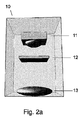
図2aは、光源11、SLM12としての透過型LCD、及び、投影レンズ13を備えた、SLM露光ユニット10の第1の例を示す。SLMとしてのLCDの動作のために必要とされる偏光素子は、SLMの一部であると想定され、示されない。偏光素子は、SLMの一部とみなされるが、必ずしもLCDと物理的に接触する必要はない。LCDの入口偏光子は、光源11とLCD12との間の任意の場所に存在してもよいが、LCDに同様に積層され得る。別個の偏光子の代わりに、光源が偏光光を発することも可能である。出口偏光子は、LCDとSLM露光ユニットの焦点面との間の任意の場所に存在してもよい。例えば、出口偏光子は、LCDに取り付けられてもよいが、SLM露光ユニットの任意のハウジングの外側の、照射される基板の位置の近くにも、同様に存在することができる。
FIG. 2 a shows a first example of a
反射型LCDがSLMとして使用される場合、光源の位置は図2aの例の位置と比較して変化し、SLMの一部としての偏光素子は、偏光ビームスプリッタなどの、反射型LCDに固有なものとなり得る。 When a reflective LCD is used as the SLM, the position of the light source changes compared to the position of the example of FIG. 2a, and a polarizing element as part of the SLM is inherent in the reflective LCD, such as a polarizing beam splitter. It can be a thing.
LCDがSLMとして使用される場合には、SLM光は既に偏光し、その結果、SLM露光ユニットは第1の偏光面を有する空間変調されたアライニング光を提供する。 If the LCD is used as an SLM, the SLM light is already polarized so that the SLM exposure unit provides spatially modulated aligning light having a first polarization plane.
図2bは、SLM21としてのDMD、光源22、投影レンズ23、及び、偏光子24を備えた、SLM露光ユニット20の第2の例を示す。偏光子は、先に記載したような任意のタイプであり得、光源からアライニング光に暴露される基板までの光路の任意の場所に位置決定され得る。図2bのSLM露光ユニットは、第1の偏光面を有する空間変調されたアライニング光を提供する。
FIG. 2 b shows a second example of the
好ましい実施形態では、SLM露光ユニットは、第1、及び、第2の偏光面を有したアライニング光を順次に提供することができる。複数の偏光面を有したアライニング光を順次に提供することができるSLM露光ユニットがより好ましい。複数の偏光面を提供することは偏光素子によって達成され得、偏光面は、異なる方向へ、又は、受動的な光学リターダ、又は、LCDなどの、偏光光の偏光面を変化させることができる受動若しくは能動光学素子によって、調節され得る。第1の偏光面と第2以上の偏光面との間の好ましい角度範囲は、35度〜55度、及び、80度〜100度であるが、生成される所望のアライメントパターンに応じて、任意の他の角度が同様に使用され得る。好ましくは、第2の、又は、複数の偏光面を提供するこのような手段は、例えばコンピュータによって、自動で制御され得る。これにより、好ましくはコンピュータによって制御された、アライニング光の異なる偏光面、及び、異なる空間変調パターンをそれぞれ有する、第1の、第2の、更には複数の照射を自動で実行することが可能となる。 In a preferred embodiment, the SLM exposure unit can sequentially provide aligning light with first and second polarization planes. More preferably, an SLM exposure unit capable of sequentially providing aligning light having a plurality of polarization planes. Providing multiple polarization planes can be achieved by polarization elements, which can be in different directions or passively capable of changing the polarization plane of polarized light, such as a passive optical retarder or LCD. Or may be adjusted by active optics. Preferred angle ranges between the first polarization plane and the second or more polarization planes are 35 to 55 degrees and 80 to 100 degrees, but are arbitrary depending on the desired alignment pattern to be generated Other angles of can be used as well. Preferably, such means for providing a second or multiple planes of polarization can be controlled automatically, for example by a computer. Thereby, it is possible to automatically execute the first, second, and a plurality of irradiations, each having different polarization planes of aligning light and different spatial modulation patterns, preferably controlled by a computer. It becomes.
第2の、又は、複数の偏光面のアライニング光を提供するために、偏光子は移動可能、及び/又は、回転可能であってもよい。例えば、偏光される光の光路の内外に交互に移動することが可能な、異なる偏光方向をそれぞれが提供するように調節された2つ以上の偏光子が存在してもよい。異なる偏光子は別個の部品でも、又は、単一のデバイスに一体化されてもよく、結果として、2つ以上の領域が異なる偏光方向を呈する。例えば、異なる偏光方向を有した偏光エリアを呈する可撓性基板の端部が、エンドレスループを形成するために、互いに固定されてもよい。異なる偏光面を有するアライニング光を順次に提供するために、異なる偏光エリアが、例えば周期的に、光路の内外に移動することができるように、偏光エリアを有するこのようなエンドレス基板は位置決定され、及び、回転することができる。異なる偏光子、及び/又は、偏光エリアを移動させる代わりに、偏光子が、回転可能なステージに載置されてもよい。これにより、異なる偏光面を順次に提供するために、偏光子を回転させることができる。一例として、図2bに示されるSLM露光ユニットの偏光子24は、偏光方向を変化させるように回転可能であってもよい。したがって、SLM露光ユニット20はまた、第2の、又は、複数の偏光面を有する光を提供することができる。好ましくは、偏光子(単数、又は、複数)、及び/又は、偏光エリアの移動、又は、回転は、モータによって駆動される。有利には、モータは、電子的に制御が可能である。好ましくは、偏光子(単数、又は、複数)の移動、及び/又は、回転は、SLMの画像生成と電子的に同期する。
The polarizer may be movable and / or rotatable to provide aligning light of the second or multiple polarization planes. For example, there may be more than one polarizer, each tuned to provide different polarization directions, which can be alternately moved in and out of the light path of the light to be polarized. Different polarizers may be separate parts or be integrated into a single device, such that two or more regions exhibit different polarization directions. For example, the ends of the flexible substrate presenting polarization areas with different polarization directions may be fixed to one another to form an endless loop. Such an endless substrate with polarization areas is positioned so that different polarization areas can be moved in and out of the light path, for example, periodically, in order to sequentially provide aligning light with different polarization planes And can be rotated. Instead of moving different polarizers and / or polarization areas, the polarizers may be mounted on a rotatable stage. This allows the polarizer to be rotated to provide different planes of polarization sequentially. As an example, the
図2aのSLM12のように、LCDがSLMとして使用される場合、SLMの出口偏光子が、空間変調された偏光状態の空間変調された光強度への変換のために必要とされる。アライニング光の偏光面を変化させるために出口偏光子を回転させることは当然可能であるが、これは、アライニング光の空間変調、及び/又は、強度に悪影響を与える恐れがある。したがって、機能的にSLMの一部である偏光素子の偏光方向は、LCDに対して固定されることが好ましい。
As in the
第2の偏光面を有する光を提供するために、追加的な偏光子が、LCD−SLMの後の光路に組み込まれ得る。しかしながら、SLMからの光は既に偏光されているので、SLM出口偏光子の偏光方向と追加的な偏光子の偏光方向が一致しない場合には、アライニング光の強度は減少することになる。追加的な偏光子の偏光方向がSLM出口偏光子の偏光方向に対して垂直である場合には、SLMからの光は更に完全に遮断されることになる。本発明の好ましい実施形態によれば、SLMとして透過型、又は、反射型LCDを有するSLM露光ユニットは、偏光解消素子、及び、追加的な偏光子を更に備える。本明細書で使用されるような偏光解消素子は、SLM光の伝搬方向に垂直な面の偏光異方性を低減、又は、除去する機能を有する。偏光解消素子は、例えば光学リターダ、特に直線偏光光を円偏光光に変換する4分の1波長リターダであってもよく、円偏光光はSLM光の伝搬方向に垂直な面の偏光異方性を有しない。偏光解消素子の他の例は、光学拡散体、多結晶体、又は、ランダム配向液晶である。追加的な偏光子が、次いで、先に記載したように、第2の、又は、複数の偏光面を有するアライニング光を提供するために、アライニング光の強度を低減させずに、好ましくは電子的に制御されて、異なる偏光方向に定められ得る。 Additional polarizers may be incorporated into the light path behind the LCD-SLM to provide light having a second polarization plane. However, since the light from the SLM is already polarized, the intensity of the aligning light will decrease if the polarization direction of the SLM exit polarizer and the polarization direction of the additional polarizer do not match. If the polarization direction of the additional polarizer is perpendicular to the polarization direction of the SLM exit polarizer, the light from the SLM will be more completely blocked. According to a preferred embodiment of the present invention, the SLM exposure unit having a transmissive or reflective LCD as the SLM further comprises a depolarizing element and an additional polarizer. Depolarization elements as used herein have the function of reducing or eliminating polarization anisotropy in a plane perpendicular to the propagation direction of SLM light. The depolarizing element may be, for example, an optical retarder, particularly a quarter-wave retarder that converts linearly polarized light into circularly polarized light, and the circularly polarized light has polarization anisotropy in a plane perpendicular to the propagation direction of SLM light. Do not have Another example of the depolarizing element is an optical diffuser, a polycrystal, or a randomly aligned liquid crystal. Preferably, without reducing the intensity of the aligning light, the additional polarizer then provides aligning light having a second or multiple polarization planes, as described above. It can be electronically controlled to define different polarization directions.
SLM露光ユニット10のSLM12が透過型LCDである一例が、図2cに示される。図2aの露光ユニットに加えて、図2cの露光ユニットは、偏光解消素子15、及び、追加的な偏光子14を備える。偏光子14は、空間変調されたアライニング光を提供するために、異なる方向に定められ得る。
An example where the
既に上述したように、SLM露光ユニットはハウジングを必要としない。したがって、図2a〜2cに描かれるようなハウジングは、何らかの限定を意図するものではない。 As already mentioned above, the SLM exposure unit does not require a housing. Thus, the housing as depicted in FIGS. 2a-2c is not intended to be limiting in any way.
本発明の好ましい実施形態によれば、SLM露光ユニットは、偏光光の偏光面を変化させることができる光学、又は、電気光学素子を備える。このような素子は、暴露される基板への、偏光光の経路の任意の場所に位置決定され得る。例えば、図2aの露光ユニットでは、素子はSLM12の後の光路に設置され得、図2bの露光ユニットでは、素子は偏光子24の後の光路に設置され得る。したがって、第2の、又は、複数の偏光面を有する光が、偏光素子の偏光方向を異なる方向に定めずに、順次に提供され得る。
According to a preferred embodiment of the present invention, the SLM exposure unit comprises an optical or electro-optical element capable of changing the polarization plane of polarized light. Such elements can be positioned anywhere in the path of polarized light to the substrate to be exposed. For example, in the exposure unit of FIG. 2a, the element may be placed in the light path after
この目的のための受動光学素子は、例えば、移動、及び/又は、回転可能な光学リターダであってもよい。例えば、光学リターダは、偏光光の偏光面を変化させるために、偏光光の経路の内外に移動することができる。偏光光の経路に交互に移動することが可能な、別々にアラインされた光学軸方向を有する2つ以上の光学リターダを使用することも可能である。このようなリターダは別個の部品でも、又は、単一のデバイスに一体化されてもよく、結果として、2つ以上の領域が異なる光学軸の方向を有した光位相差を呈する。例えば、異なる光学軸方向を有した位相差エリアを呈する可撓性基板の端部が、エンドレスループを形成するために、互いに固定されてもよい。異なる偏光面を有するアライニング光を順次に提供するために、異なる位相差エリアが、例えば周期的に、光路の内外に移動することができるように、異なる位相差領域を有するこのようなエンドレス基板は位置決定され、及び、回転することができる。異なるリターダ、及び/又は、位相差エリアを移動させる代わりに、リターダが、回転可能なステージに載置されてもよい。これにより、異なる偏光面を順次に提供するために、リターダを回転させることができる。好ましくは、リターダ(単数、又は、複数)、及び/又は、位相差エリア(単数、又は、複数)の移動、又は、回転は、モータによって駆動される。有利には、モータは、電子的に制御が可能である。好ましくは、リターダ(単数、又は、複数)の移動、及び/又は、回転は、SLMの画像生成と電子的に同期する。好ましくは、受動光学素子は、好ましくは互いに対して移動、及び/又は、回転可能な、半波リターダ、又は、直列の2つの4分の1波長リターダを含む。 Passive optical elements for this purpose may, for example, be movable and / or rotatable optical retarders. For example, an optical retarder can be moved in and out of the path of polarized light to change the polarization plane of the polarized light. It is also possible to use two or more optical retarders with separately aligned optical axis directions, which can be moved alternately in the path of polarized light. Such retarders may be separate parts or be integrated into a single device, such that two or more regions exhibit optical retardation with different optical axis orientations. For example, the ends of the flexible substrate presenting retardation areas with different optical axis directions may be fixed to one another to form an endless loop. Such an endless substrate with different retardation regions, such that different retardation areas can be moved in and out of the light path, for example periodically, to sequentially provide aligning light with different polarization planes Can be positioned and rotated. Instead of moving different retarders and / or retardation areas, the retarders may be mounted on a rotatable stage. This allows the retarder to be rotated to provide different polarization planes sequentially. Preferably, movement or rotation of the retarder (s) and / or the retardation area (s) is / are driven by a motor. Advantageously, the motor can be controlled electronically. Preferably, the movement and / or rotation of the retarder (s) are / is electronically synchronized with the imaging of the SLM. Preferably, the passive optical elements preferably include half-wave retarders, or two quarter-wave retarders in series, which are movable and / or rotatable relative to each other.
偏光光の偏光面を変化させるために適切な電気光学素子は、例えば偏光子のない液晶(LC)セルであり、液晶の構成、及び/又は、実効複屈折がセルの電極への電圧の印加によって修正される。液晶セルのタイプ、及び、構成に応じて、偏光光の偏光状態、及び/又は、偏光方向の両方が、液晶セルを通過することによって変化し得る。例えば、液晶セルが捩れネマチックタイプであり、到来する光が直線偏光される場合には、液晶がセルへの電圧の印加によって垂直構成に切り替えられる限り、液晶セルを通過する際の偏光方向は変化しない。しかしながら、電圧が液晶セルに印加されない場合には、セルが導波条件を満たし、セルが適宜到来する光の偏光方向に対してアラインされるのであれば、液晶は、到来する偏光光の偏光方向をツイストの角度によって回転させるツイストした構成を形成する。同様に、垂直にアラインされた(VA)タイプのLCセルが、使用され得る。電圧がセルに印加されない限り、VA−LCセルは光の偏光状態に影響を及ぼさない。セルに対する電圧の印加の際に、液晶セルが入射する偏光光のために複屈折となるように、液晶は異なる構成へ切り替わる。セルパラメータ、及び、電圧が正確に選択される場合には、偏光光の偏光面はセルを通過する際に変化する。好ましくは、光の偏光面を変化させるための電圧が印加されるときに、VA−LCセルは、半波リターダとしての機能を果たす。 A suitable electro-optic element for changing the polarization plane of the polarized light is, for example, a liquid crystal (LC) cell without a polarizer, where the composition of the liquid crystal and / or the effective birefringence is applied to the electrode of the cell. Corrected by Depending on the type and configuration of the liquid crystal cell, both the polarization state of the polarized light and / or the polarization direction can be changed by passing through the liquid crystal cell. For example, if the liquid crystal cell is of the twisted nematic type and the incoming light is linearly polarized, the polarization direction changes as it passes through the liquid crystal cell as long as the liquid crystal is switched to the vertical configuration by the application of voltage to the cell. do not do. However, if a voltage is not applied to the liquid crystal cell, the cell meets the guiding conditions and if the cell is properly aligned with the polarization direction of the incoming light, then the liquid crystal is the polarization direction of the incoming polarization light A twisted structure is formed in which the is rotated by the twist angle. Similarly, vertically aligned (VA) type LC cells may be used. As long as no voltage is applied to the cell, the VA-LC cell does not affect the polarization state of the light. Upon application of a voltage to the cell, the liquid crystal switches to a different configuration so that the liquid crystal cell is birefringent due to the incident polarized light. If the cell parameters and voltage are selected correctly, the polarization plane of the polarized light will change as it passes through the cell. Preferably, the VA-LC cell acts as a half wave retarder when a voltage is applied to change the polarization plane of the light.
液晶セルの代わりに、他の電子、又は、磁気制御可能な手段が、例えば磁気光学ファラデー効果を使用して、光の偏光方向を修正するために使用され得る。 Instead of liquid crystal cells, other electronic or magnetically controllable means can be used to modify the polarization direction of light, for example using the magneto-optical Faraday effect.
電気光学素子が偏光光の偏光面を変化させるために使用される場合には、偏光子の、又は、リターダなどの受動偏光回転素子の機械的な調節が回避可能であり、異なる偏光面間の切り替えが非常に速い。 If an electro-optical element is used to change the polarization plane of the polarized light, mechanical adjustment of the polarizer or of a passive polarization rotation element such as a retarder can be avoided and between the different polarization planes Switching is very fast.
本発明の好ましい実施形態では、SLM露光ユニットは、SLMとしてのDMD、SLMの照明のための光を提供する2つの光源を備え、2つの光源から発する光は、2つの異なる偏光面でそれぞれ偏光され、その後SLMに到達する。この目的のために、光源自体が偏光光を提供してもよく、又は、偏光子が光源とSLMとの間の光路に配置されてもよい。2つの光源の光は、例えば、SLMを順次に照らすことができる。同時に、SLMに適用されるパターンが変化してもよく、結果として、露光ユニットは異なるパターン、及び、偏光方向を有する空間変調されたアライニング光を順次に提供することができる。好ましくは、SLMの照明のための起点は、第1、及び、第2の光源間で周期的に変化し、結果として、SLMに到達する光の偏光方向は周期的に変化し続ける。この変化は、例えば、第1、及び、第2の光源からの光を、例えば機械的、又は、光電子シャッタにより、交互に遮断することによって実行され得る。2つの光源からの光を交互に遮断する代わりに、例えば周期的に、光源がオン/オフに交互に切り替えられてもよい。好ましくは、LEDが2つの光源のために使用される。 In a preferred embodiment of the present invention, the SLM exposure unit comprises two light sources that provide light for illumination of the SLM, the DMD as the SLM, and the light emitted from the two light sources is respectively polarized in two different planes of polarization. And then reach the SLM. For this purpose, the light source itself may provide polarized light, or a polarizer may be arranged in the light path between the light source and the SLM. The light from the two light sources can, for example, sequentially illuminate the SLM. At the same time, the pattern applied to the SLM may change, and as a result, the exposure unit can sequentially provide different patterns and spatially modulated aligning light having a polarization direction. Preferably, the origin for illumination of the SLM changes periodically between the first and second light sources, and as a result, the polarization direction of the light reaching the SLM continues to change periodically. This change may be performed, for example, by alternately blocking the light from the first and second light sources, for example by means of a mechanical or optoelectronic shutter. Instead of alternately blocking the light from the two light sources, the light sources may be switched on / off alternately, for example periodically. Preferably, LEDs are used for the two light sources.
本発明の別の好ましい実施形態では、装置は、第2の偏光面のアライニング光を提供する追加的な偏光源を備える。 In another preferred embodiment of the invention, the device comprises an additional polarization source providing aligning light of the second polarization plane.
好ましくは、追加的な偏光源もまた、SLM露光ユニットである。2つのSLM露光ユニットから発せられるアライニング光の偏光面は、同一であってもよく、又は、互いに異なる。好ましくは、2つの露光ユニットの投影エリアが、互いに重なり、同一であり得るように、SLM露光ユニットは配置される。これにより、基板、又は、基板のための支持体を移動させずに、同時に、又は、順次に2つの露光ユニットのアライニング光に層を暴露することができる。 Preferably, the additional polarization source is also an SLM exposure unit. The polarization planes of the aligning light emitted from the two SLM exposure units may be identical or different from one another. Preferably, the SLM exposure units are arranged so that the projection areas of the two exposure units can overlap and be the same. This allows the layer to be exposed to the aligning light of the two exposure units simultaneously or sequentially without moving the substrate or the support for the substrate.
本発明の別の好ましい実施形態では、装置は2つのSLM露光ユニットを備え、LCMO層に傾斜角を誘発するためにそれぞれのアライニング光が斜めの角度で基板面に投射されるように、SLM露光ユニットの一方、又は、両方が配置される。好ましくは、両方の露光ユニットのアライニング光が斜めの角度で基板面に投射され、両方の露光ユニットからのアライニング光の入射面が互いに平行か、又は、互いに一致する。このような実施形態のために、斜めの角度が基板面の法線に対して対称であることが好ましい。上で使用されるような入射面とは、アライニング光の平均伝搬方向、及び、基板面の法線によって画定される面を意味する。 In another preferred embodiment of the present invention, the apparatus comprises two SLM exposure units, so that each aligning light is projected onto the substrate surface at an oblique angle to induce a tilt angle in the LCMO layer. One or both of the exposure units are arranged. Preferably, the aligning light of both exposure units is projected onto the substrate surface at an oblique angle, and the incident surfaces of the aligning light from both exposure units are parallel to each other or coincide with each other. For such embodiments, it is preferred that the oblique angle be symmetrical with respect to the normal to the substrate surface. By incident surface as used above is meant the surface defined by the average propagation direction of the aligning light and the normal to the substrate surface.
アライニング光の偏光面を照射の前に一定の角度に設定する代わりに、アライニング光の空間変調を経時的に変化させながら、偏光面を継続的に回転させてもよい。したがって、本発明による装置のSLM露光ユニットは、継続的に回転することができる、アライニング光の偏光面を変化させることが可能な偏光子14、若しくは、24、又は、光学素子を備えてもよい。
Instead of setting the polarization plane of the aligning light at a certain angle before irradiation, the polarization plane may be continuously rotated while changing the spatial modulation of the aligning light with time. Thus, the SLM exposure unit of the device according to the invention may also be provided with a
基板のバッチ処理のために設計される装置では、例えば基板の一定の縁部と平行な線によって画定され得る基板の方向が、アライニング光の偏光面に対して、異なる角度に調節可能であってもよい。これは、アライニング光に第2の偏光面を提供することの変形例となる。この目的のために、基板のための支持体が回転可能であることが好ましい。 In an apparatus designed for batch processing of substrates, for example, the direction of the substrate, which can be defined by a line parallel to a certain edge of the substrate, can be adjusted to different angles with respect to the polarization plane of the aligning light. May be This is a modification of providing the second polarization plane for the aligning light. For this purpose it is preferred that the support for the substrate is rotatable.
本発明の好ましい実施形態によれば、装置は、先に記載したような1つ以上のSLM露光ユニット、及び、任意に追加的な偏光源、更にLCMO層、及び/又は、従材料の層を適用するためのコーティング、又は、印刷ユニットを備える。理想的には、装置は、LCMO層を適用する1つと従材料を適用するもう1つの、コーティング、及び/又は、印刷のための2つのユニットを備える。原理上、装置の大きさに適合する限り、任意のタイプのコーティング、又は、印刷方法が使用可能である。使用可能なコーティング技術としては、スピンコーティング、ブレードコーティング、ナイフコーティング、キスロールコーティング、リバースキスコーティング、キャストコーティング、しごきコーティング、浸漬、はけ塗り、ローラーコーティング、流し塗り、射出成形、ワイヤコーティング、スプレーコーティング、デイップコーティング、旋回コーティング、エアーナイフコーティング、リバースロールコーティング、グラビアコーティング、スロットダイコーティング、ホットメルトコーティング、ローラーコーティング、又は、フレキソコーティングが挙げられるが、これらに限定されない。使用可能な印刷技術としては、シルクスクリーン印刷、凸版印刷、フレキソ印刷、ジェット印刷、凹版印刷、直接グラビア印刷、オフセットグラビア印刷、リソグラフ印刷、オフセット印刷が挙げられるが、これらに限定されない。好ましい方法は、ローラーコーティング、スロットダイコーティング、オフセット印刷、及び、ジェット印刷である。 According to a preferred embodiment of the present invention, the apparatus comprises one or more SLM exposure units as described above, and optionally an additional polarization source, in addition an LCMO layer and / or a layer of slave material. A coating or printing unit for application is provided. Ideally, the device comprises two units for coating and / or printing, one for applying the LCMO layer and the other for applying the secondary material. In principle, any type of coating or printing method can be used as long as it fits the size of the device. Available coating technologies include spin coating, blade coating, knife coating, kiss roll coating, reverse kiss coating, cast coating, iron coating, dipping, brushing, roller coating, flow coating, injection molding, wire coating, and spraying. Examples include, but are not limited to, coating, dip coating, swirl coating, air knife coating, reverse roll coating, gravure coating, slot die coating, hot melt coating, roller coating, or flexo coating. Usable printing techniques include, but are not limited to, silk screen printing, letterpress printing, flexographic printing, jet printing, intaglio printing, direct gravure printing, offset gravure printing, lithographic printing, and offset printing. Preferred methods are roller coating, slot die coating, offset printing, and jet printing.
本発明によれば、装置は、1つ以上の加熱ステージを更に備えてもよく、加熱ステージは、残留溶媒を除去するべく、及び/又は、簡単な配向のためにLCMOの、及び/又は、従材料の粘度を減少させるべく、コーティングを既定の温度まで加熱するために使用され得る。更に、加熱ステージは、従材料の重合を開始するために使用されてもよい。加熱ステージは、例えば赤外線加熱器、温風送風機、オーブン、マイクロ波、又は、熱板を使用して、熱を生成し、伝達する公知の手段を使用することができる。装置がバッチ処理のために設計される場合には、支持体自体が加熱可能であってもよい。 According to the invention, the apparatus may further comprise one or more heating stages, which are for removing residual solvent and / or of the LCMO and / or for easy orientation. It can be used to heat the coating to a predetermined temperature to reduce the viscosity of the secondary material. Furthermore, a heating stage may be used to initiate the polymerization of the secondary material. As the heating stage, for example, an infrared heater, a hot air blower, an oven, a microwave, or a hot plate can be used, and known means for generating and transferring heat can be used. If the device is designed for batch processing, the support itself may be heatable.
装置は、従材料の重合を開始するための化学線光を提供する硬化ユニットとして追加的な光源を更に備えてもよい。好ましくは、光源は、420nm未満の波長領域の光を提供する。好ましいタイプの光源は、UV−LEDなどのLED、及び、高圧水銀ランプである。 The apparatus may further comprise an additional light source as a curing unit that provides actinic light for initiating polymerization of the slave material. Preferably, the light source provides light in the wavelength region below 420 nm. Preferred types of light sources are LEDs, such as UV-LEDs, and high pressure mercury lamps.
好ましくは、ステージが装置に存在する限り、本発明による装置は、SLM露光ユニット、追加的な光源、コーティング、又は、印刷ユニットのステージ、及び、加熱ステージなどの、装置の異なるステージの所望の位置に基板を移動させる手段を備える。基板の移動が、自動処理を可能にするために、例えばコンピュータによって、電子的に制御が可能であることが好ましい。 Preferably, as long as the stage is present in the apparatus, the apparatus according to the present invention is a desired position of different stages of the apparatus, such as SLM exposure unit, additional light source, coating or printing unit stage, and heating stage. Means for moving the substrate. The movement of the substrate is preferably electronically controllable, for example by a computer, in order to allow automatic processing.
図3に示される本発明による装置30の例は、第1のコーティング、又は、印刷ユニット33、第2のコーティング、又は、印刷ユニット34、SLM露光ユニット31、ヒータ35、硬化ユニット36、基板39のための支持体37、及び、摺動プロファイル38を備える。支持体37は、支持体上の基板を装置の異なるユニットへ位置決定するために、摺動プロファイル38に沿って移動することができる。好ましくは、支持体の移動はコンピュータによって制御されるが、コンピュータは図3に示されない。SLM露光ユニット31は、第1の、及び、第2の偏光面を有するアライニング光を提供する手段を有した、先に記載したユニットのいずれかであり得る。露光ユニットのSLMはコンピュータによって好ましくは制御されるが、同様にコンピュータは図3に示されない。ヒータ35は、例えば、赤外線加熱器、又は、温風送風機であり得る。硬化ユニット36は、従材料の重合を開始するための化学線光を提供する光源を備える。
The example of the
図3に示されるような装置では、第1のコーティング、又は、印刷ユニット33はLCMO層を基板に適用するために使用され、第2のコーティング、又は、印刷ユニット34は従材料をコーティング、又は、印刷するために使用され得る。製造プロセスは、この場合、例えば、以下の通りとなり得る。基板39を支持体37上に位置決定すること、基板を有した支持体を第1のコーティング、又は、印刷ユニット33の下に移動させること、光配向可能材料を含んだ溶液を基板にコーティング、又は、印刷すること、残留する溶媒を除去するために支持体をヒータ35へ移動させること、支持体を露光ユニット31へ移動させること、露光ユニットの偏光面を第1の方向に設定すること、所望のパターンを提供するために露光ユニットのSLMにアドレスすること、露光ユニットの空間変調されたアライニング光を基板上のLCMO層に照射すること、露光ユニットの偏光面を第2の方向に設定すること、所望のパターンを提供するため、又は、すべてのピクセルをオン状態に切り替えるために露光ユニットのSLMにアドレスすること、露光ユニットのアライニング光を基板に照射すること、支持体を第2のコーティング、又は、印刷ユニット34へ移動させること、基板のLCMO層上に従材料を適用すること、基板の温度を上昇させるために支持体をヒータ35の下方に移動させること、基板を有した支持体を硬化ユニットへ移動させること、及び、従材料の重合のために化学線光を提供すること。液晶材料のタイプによっては、重合は、不活性雰囲気下で実行されなければならない場合がある。図3による装置を使用した上記のプロセスは、コンピュータによって制御されても、完全に自動であってもよい。
In an apparatus as shown in FIG. 3, a first coating or
バッチ処理のために同様に設計される本発明による代替実施形態では、装置は、基板を装置の異なるステージへ搬送するために、ロボットアーム、又は、任意の他の適切な取扱システムを備える。内部の基板搬送の他に、取扱システムはまた、装置の内側、又は、外側に配置された基板の重ね合わせから処理される基板を持ち上げるために、及び/又は、処理した基板を界面取扱システムへ送出するか、又は、所望の位置に堆積させるために使用されてもよい。ロボットアームなどの基板取扱システムは、コンピュータによって好ましくは制御される。このような構成は、例えば、すべての基板搬送、及び、調節工程、照射、コーティング、及び/又は、印刷、層の乾燥、従材料の重合、並びに、基板の入出の管理を含んだ、基板の自動処理を可能にする。一例として、自動カセットツーカセット処理が実行可能である。 In an alternative embodiment according to the invention, which is also designed for batch processing, the apparatus comprises a robotic arm or any other suitable handling system to transport the substrate to different stages of the apparatus. In addition to internal substrate transport, the handling system may also be used to lift substrates to be processed from the stack of substrates placed inside or outside the apparatus, and / or to handle interfaced substrates to the interface handling system. It may be delivered or used to deposit at the desired location. A substrate handling system such as a robot arm is preferably controlled by a computer. Such arrangements include, for example, all substrate transport and conditioning processes, irradiation, coating and / or printing, layer drying, secondary material polymerization, and substrate entry / exit management. Enable automatic processing. As an example, automatic cassette to cassette processing can be performed.
基板取扱システムとしてのロボットアームを備える装置40の一例が、図4に示される。装置は、第1のコーティング、又は、印刷ユニット43、第2のコーティング、又は、印刷ユニット44、第1の偏光面を有する空間変調されたアライニング光を提供するSLM露光ユニット41、第2の偏光面を有するアライニング光を提供する偏光源42、オーブン45、硬化ユニット46、基板47のための支持体、ロボットアーム48、並びに、入出基板を格納するカセット49、及び、50を備える。ロボットアーム48に接続される支持体47は、例えば穴、又は、チャネルを通過して適用される真空によって実行され得る、基板51を持ち上げ固定する手段を有する。ロボットアームは、支持体を異なる処理ユニットへ移動させる。ロボットアームと同様に異なる処理ユニットもコンピュータ制御され、結果として、個別にパターン化された異方性を有する素子の完全に自動的な製造がカセットからカセットへと実行され得る。単純化の理由により、コンピュータ、並びに、電気、及び、機械的接続は、図に示されない。SLM露光ユニット41は、先に記載したSLM露光ユニットのいずれかであってもよい。偏光源42は、SLM露光ユニット41により提供されるアライニング光の偏光面とは異なる偏光面を有する他、均一な光強度を有するアライニング光を提供する。硬化ユニット46は、従材料の重合反応を開始するための化学線光を提供する光源を備える。
An example of a
図4に示されるような装置では、第1のコーティング、又は、印刷ユニット43はLCMO層を基板に適用するために使用され、第2のコーティング、又は、印刷ユニット44は従材料をコーティング、又は、印刷するために使用され得る。カセット49に処理される基板を提供した後、自動的な製造プロセスは、この場合、例えば、以下の通りとなり得る。基板51をロボットアーム48に接続された支持体47でカセット49から持ち上げること、基板を有した支持体を第1のコーティング、又は、印刷ユニット43の下に移動させること、光配向可能材料を含んだ溶液を基板51にコーティングすること、残留する溶媒を除去するためにコーティングされた基板を有する支持体をオーブン45に位置決定すること、基板を有する支持体を露光ユニット41へ移動させること、所望のパターンを提供するために露光ユニットのSLMにアドレスすること、露光ユニットの空間変調されたアライニング光を基板上のLCMO層に照射すること、基板を有する支持体を偏光源42へ移動させること、LCMO層を偏光源42のアライニング光に暴露すること、支持体を第2のコーティング、又は、印刷ユニット44へ移動させること、基板の照射されたLCMO層上へ従材料を適用すること、基板を有する支持体をオーブン45に位置決定し、基板を有する支持体を硬化ユニットへ移動させる、及び、従材料の重合を開始するための化学線光を提供すること。従材料のタイプによっては、重合は、不活性雰囲気下で実行されなければならない場合がある。
In the apparatus as shown in FIG. 4, the first coating or
図5は、本発明による装置の一例を示す。装置は、リールツーリール製造における、第1の偏光面を有する空間変調されたアライニング光での、及び、第2の偏光面のアライニング光での、可撓性基板の、又は、可撓性基板上の光配向可能材料の順次照射のために設計される。図5の装置60は、第1の偏光面を有する空間変調されたアライニング光を提供するSLM露光ユニット61、第2の偏光面を有するアライニング光を提供する偏光源62、並びに、基板63のための支持体64、及び、65を備える。支持体64、及び、65は、リールツーリールで基板を移動させることができるようにされる。単純な実施形態では、この移動は、例えばクランクを使用して一方、又は、両方の支持体を回転させるによって、手動で実行される。好ましくは、支持体64、及び、65の一方、又は、両方が、モータによって駆動される。基板は、支持体64から支持体65へと、又は、反対方向へと移動することができる。装置60はコーティングユニットを備えないので、基板が例えば基板に前コーティングされたLCMO層を含んでもよく、又は、LCMO層自体が基板として形成される。SLM露光ユニット61は、先に記載したSLM露光ユニットのいずれかであってもよい。偏光源62は、SLM露光ユニット61により提供されるアライニング光の偏光面とは異なる偏光面を有する他、均一な光強度を有するアライニング光を提供し、SLMを備える必要はない。
FIG. 5 shows an example of a device according to the invention. The device is or is flexible in a reel-to-reel manufacture with a spatially modulated aligning light with a first polarization plane and with a second polarization plane aligning light. Designed for sequential illumination of photoalignable materials on flexible substrates. The
リールツーリール製造のための装置は、例えば、光配向可能材料をコーティング若しくは印刷するユニット、及び/又は、従材料をコーティング、又は、印刷するユニットなどの、追加的なユニット、並びに、任意に、オーブン、赤外線加熱器、又は、温風送風機などの、基板の温度を局所的に上昇させる手段を備えてもよい。図6は、本発明による装置70の一例を示す。装置は、基板73のための支持体74、及び、75、第1のコーティング、又は、印刷ユニット76、オーブン78、第1の偏光面を有する空間変調されたアライニング光を提供するSLM露光ユニット71、第2の偏光面を有するアライニング光を提供する偏光源72、第2のコーティング、又は、印刷ユニット77、オーブン79、硬化ユニット80、並びに、処理される可撓性基板を誘導、及び、支持するロール81を備える。SLM露光ユニット71は、先に記載した露光ユニットのいずれかであってもよい。偏光源72は、露光ユニット71により提供されるアライニング光の偏光面とは異なる偏光面を有する他、均一な光強度を有するアライニング光を提供する。硬化ユニット80は、従材料の重合を開始するための化学線光を提供する光源を備える。支持体74、及び、75は、支持体74のリールから支持体75のリールまで基板を移動させることができるようにされる。好ましくは、支持体74、及び、75の一方、又は、両方は、モータによって駆動される。装置70は、パターン化された異方性を有する素子の完全に自動的な製造を可能にする。
An apparatus for reel-to-reel manufacturing includes, for example, an additional unit, such as a unit that coats or prints a photo-alignable material and / or a unit that coats or prints a slave material, and optionally, A means may be provided to locally raise the temperature of the substrate, such as an oven, an infrared heater or a hot air blower. FIG. 6 shows an example of a
図5、及び、図6の例のようなリールツーリール処理のための装置では、基板は、継続的に移動してもよいし、又は、空間変調されたアライニング光での照射のために少なくとも露光ユニット61、71の位置で止められてもよい。基板が露光ユニット61、71の投影エリア内で継続的に移動する場合には、空間変調された光により提供されるパターンが動きぼけなくLCMO層の層に再現されるように注意することが重要であり得る。例えば、パターンで照射される基板のエリアがSLM露光ユニットの投影エリアに接近する度に、フラッシュとして空間変調された光を提供することによって、これは実行され得、結果として、パターンが単一のフラッシュの短時間内にLCMO層に再現される。代替的に、SLMにより提供されるパターンが、基板の移動と同期してスクロールする。この目的のために、基板の速度、又は、支持体64、65、74、75、又は、誘導ロール81の回転速度が、スクロールするパターン生成を制御する電気信号をSLMに提供するために、適切な手段によって監視され得る。マトリックスタイプのSLMでは、スクロールはライン毎に好ましくは実行される。これは、SLMが適用されたパターンを1ラインずつ周期的に移動させることを意味し、結果として、アライニング光の空間変調が基板と同期して移動する。
In an apparatus for reel-to-reel processing such as the example of FIGS. 5 and 6, the substrate may be moved continuously or for illumination with spatially modulated aligning light. It may be stopped at least at the position of the
図6の装置などの、装置を使用した場合、個別にパターン化された異方性を有する素子を製造するためのプロセスは、以下の工程を含み得る。リールツーリール製造のための装置における可撓性基板73を支持体74のリール上に準備し、基板が移動し支持体75のリール上へ行き着くように装置を操作すること、光配向可能材料を含む溶液をコーティング、又は、印刷ユニット76で基板73にコーティング、又は、印刷すること、残留する溶媒を除去するために基板をオーブン78で加熱し、個別の情報のスクロールパターンを提供するために露光ユニット71のSLMにアドレスすることで投射されるパターンが基板73と同一の速さ、及び、方向でSLM露光ユニット71の投影エリア内で移動すること、露光ユニット71からの第1の偏光面の空間変調されたアライニング光を基板上のLCMO層に照射すること、偏光源72からの第2の偏光面のアライニング光を基板上のLCMO層に照射すること、コーティング、又は、印刷ユニット77で照射されたLCMO層上に従材料をコーティング、又は、印刷すること、任意に基板をオーブン79で加熱すること、従材料の重合を硬化ユニット80の化学線光への暴露によって開始し、処理した基板を支持体75のリール上に巻き上げること。従材料のタイプによっては、重合は、不活性雰囲気下で実行されなければならない場合がある。
When using a device, such as the device of FIG. 6, the process for manufacturing a device with individually patterned anisotropy may include the following steps. Preparing the
図7は、図6の装置70の変形例であり追加的にパージユニット82を備えた装置90を示す。パージユニット82では、非重合化合物が処理された層から除去され得る。パージユニットは、典型的に、非重合化合物を溶解することが可能な溶媒を収容する。
FIG. 7 shows a
LCMO層が、最初にSLM露光ユニット61、71の空間変調されたアライニング光に暴露され、次いで偏光源62、72からの第2の偏光面のアライニング光に暴露されてもよいので、基板移動の方向に対するSLM露光ユニット61、71の、及び、偏光源62、72の順次の配置は置き換えられてもよい。
Since the LCMO layer may be first exposed to the spatially modulated aligning light of the
図5の例での装置は、予め準備されたLCMO層での個別のパターンのリールツーリール生成のためだけに設計され、図6の装置は、必要なコーティング工程を含み、個別にパターン化された異方性を有する素子を自動で製造することを可能にするが、本発明によるリールツーリール製造装置は、1つのコーティング工程を含むだけでもよい。例えば、装置は、光配向可能材料を含む層を適用するコーティングユニット76、及び、オーブン78を備えるが、コーティングユニット77、オーブン79、及び、硬化ユニット80を備えなくてもよい。このような装置では、LCMO層は適用され、個別のパターンがLCMO層に生成され得る。従材料の任意の層は、次いで、別個の装置で、コーティングされ任意に重合されなければならない。同様に、本発明によるリールツーリール装置は、照射されたLCMO層上に従材料の層を生成するコーティングユニット77、オーブン79、及び、硬化ユニット80を備えてもよい。このような装置で使用するために、基板がLCMO層で前コーティングされてもよく、又は、LCMO層が基板として形成されてもよい。SLM露光ユニット71、及び、偏光源72への暴露によって必要な配向パターンを生成した後に、従材料が、コーティング、又は、印刷ユニット77によってコーティング、又は、印刷され、オーブン79で乾燥、及び、配向され、硬化ユニット80で重合されて、結果として、個別にパターン化された異方性を有する所望の素子がもたらされる。
The device in the example of FIG. 5 is designed only for reel-to-reel generation of individual patterns in the pre-prepared LCMO layer, the device of FIG. 6 includes the necessary coating steps and is individually patterned Although it is possible to automatically manufacture elements having different anisotropy, the reel-to-reel manufacturing apparatus according to the present invention may only include one coating step. For example, the apparatus comprises a
上記の実施形態のいずれかによる装置は、例えば永続的な情報を印刷する手段、又は、装置で製造された素子を他の基板若しくはデバイスに積層する手段などの、ユニットを更に備えてもよい。 The device according to any of the above embodiments may further comprise a unit, such as, for example, means for printing permanent information or means for laminating the device produced in the device to another substrate or device.
本発明による装置は、ユニットの一定の組み合わせなどの、一定の実施形態に制限されない。それよりもむしろ、異なるタイプの露光ユニット、コーティング、又は、印刷ユニット、加熱ステージ、化学線光源、基板のための支持体、及び、基板取扱システムが、自由に装置に組み合わせられ得る。 The device according to the invention is not limited to certain embodiments, such as certain combinations of units. Rather, different types of exposure units, coating or printing units, heating stages, actinic light sources, substrates for substrates, and substrate handling systems can be freely combined in the apparatus.
本発明は、更に、個別にパターン化された異方性を有する素子を高速に製造するための方法に関する。本発明による方法は、
− LCMO層を準備する工程と、
− 第1の偏光面を有するSLM露光ユニットの空間変調されたアライニング光にLCMO層を暴露する工程と、を含む。
The invention further relates to a method for the rapid production of devices with individually patterned anisotropy. The method according to the invention is
-Preparing a LCMO layer;
Exposing the LCMO layer to spatially modulated aligning light of an SLM exposure unit having a first plane of polarization.
LCMO層は、コーティング、及び/又は、印刷によって適用されてもよく、基板のエリア全体に、又は、エリアの一部だけに提供されてもよい。 The LCMO layer may be applied by coating and / or printing, and may be provided over the entire area of the substrate or only a portion of the area.
先に記載したような方法で、LCMO層に更なるアライメント処理が施されない場合には、LCMO層はアライニング光に暴露されたエリアでだけ異方性を呈する。したがって、LCMO層に、又は、LCMO層上に備えられた従材料は、アライニング光に暴露されたLCMO層のエリアでだけLCMO材料との接触のために異方性を確立し、それらのエリアの外側では異方性は創出されない。LCP材料が従材料として使用される場合には、このように製造されるパターン化された異方性を有する素子は、したがって、液晶材料がアラインされるエリア、及び、液晶材料がアラインされないエリアを含む。このように生成されるパターンは、偏光光に見ることができる。 In the manner described above, if the LCMO layer is not further aligned, the LCMO layer exhibits anisotropy only in areas exposed to aligning light. Thus, the slave material provided on or on the LCMO layer establishes anisotropy for contact with the LCMO material only in the area of the LCMO layer exposed to the aligning light, and those areas Anisotropy is not created outside of. In the case where LCP material is used as a secondary material, the device with patterned anisotropy produced in this way therefore has an area in which the liquid crystal material is aligned and an area in which the liquid crystal material is not aligned. Including. The pattern generated in this way can be seen in polarized light.
ピクセルのそれぞれがオン、又は、オフ状態であるようにSLMがアドレスされてもよく、アライニング光の空間的変化が、強度が最も低いレベルか、又は、最も高いレベルを有するようにされるという結果がもたらされる。このようなSLM−アドレス方式は、以下、デジタルアドレッシングと称される。代替的に、オン、及び、オフ状態の間の中間状態にピクセルをアドレスすることが可能であり、アライニング光の空間的変化がグレーレベルも備えるという結果がもたらされる。このようなSLM−アドレス方式は、以下、グレースケールアドレッシングと称される。 The SLM may be addressed so that each of the pixels is in the on or off state, and the spatial variation of the aligning light is made to have the lowest or highest intensity level. The result is brought about. Such an SLM-addressing scheme is hereinafter referred to as digital addressing. Alternatively, it is possible to address the pixel to an intermediate state between the on and off states, resulting in the spatial variation of the aligning light also comprising a gray level. Such an SLM-addressing scheme is hereinafter referred to as grayscale addressing.
本発明の好ましい方法では、デジタルアドレッシングがSLM−アドレス方式として使用される。本発明の別の好ましい方法では、グレースケールアドレッシングがSLM−アドレス方式として使用される。 In the preferred method of the present invention, digital addressing is used as the SLM-addressing scheme. In another preferred method of the invention, grayscale addressing is used as the SLM-address scheme.
好ましい方法では、LCMO層は、第1の偏光面の空間変調されたアライニング光への暴露の前か後のどちらかに、第2の偏光面を有するアライニングに追加的に暴露される。第2の偏光面のアライニング光が、第1の偏光面のアライニング光によって照射されないエリアにだけ提供されてもよい。これは、例えば、同様にSLM露光ユニットにより、第2の偏光面のアライニング光を提供することによって実行され得る。 In a preferred method, the LCMO layer is additionally exposed to an alignment having a second polarization plane, either before or after exposure of the first polarization plane to the spatially modulated aligning light. Aligning light of the second polarization plane may be provided only in areas not illuminated by the aligning light of the first polarization plane. This can be performed, for example, by providing aligning light of the second polarization plane, also by the SLM exposure unit.
代替的に、2つの暴露工程が、LCMO層の少なくともいくつかのエリアが第1、及び、第2の偏光面のアライニング光に、いずれかの順序で、順次に暴露されるようにされる。これは、例えばSLM露光ユニットの空間変調されたアライニング光への暴露の前か後のどちらかにLCMO層を偏光源のアライニング光に暴露することによって、実行され得る。 Alternatively, the two exposure steps cause at least some areas of the LCMO layer to be sequentially exposed in either order to the aligning light of the first and second polarization planes. . This may be performed, for example, by exposing the LCMO layer to the aligning light of the polarization source either before or after exposure of the SLM exposure unit to the spatially modulated aligning light.
別の好ましい方法では、LCMO層は、複数の偏光面を有するアライニングに暴露される。第2の、及び、更なる偏光面のアライニング光は、アライニング光によってまだ照射されていないエリアにだけ提供されてもよい。好ましくは、これは、同様にSLM露光ユニットにより、第2の、及び/、又は、更なる偏光面のアライニング光を提供することによって実行される。 In another preferred method, the LCMO layer is exposed to an alignment having multiple polarization planes. Aligning light of the second and further polarization planes may be provided only in areas not already illuminated by the aligning light. Preferably, this is carried out by providing aligning light of the second and / or further polarization planes as well by the SLM exposure unit.
光配向可能材料の性質、スペクトル強度分布、及び、アライニング光の露光量に応じて、2つ以上の偏光面のアライニング光に暴露されるエリアでの結果として生じる局所的なアライメント方向が、アライニング光のどちらかの偏光面に暴露されるだけであるエリアで創出されるアライメント方向と異なってもよい。したがって、第1、第2、、又は、追加的な暴露工程での局所的な露光量によって、二重、又は、多重に暴露されたエリアでの結果として生じるアライメント方向を制御することが可能である。 Depending on the nature of the photoalignable material, the spectral intensity distribution and the exposure of the aligning light, the resulting local alignment direction in the area exposed to the aligning light of two or more polarization planes is: It may be different from the alignment direction created in the area that is only exposed to either polarization plane of the aligning light. Thus, it is possible to control the resulting alignment direction in double or multiple exposed areas by local exposure at the first, second or additional exposure steps. is there.
本発明の好ましい方法によれば、グレースケールアドレッシングが、第1の偏光面を有するアライニング光での照射のためのSLM−アドレス方式として使用され、LCMO層が第2の偏光面を有するアライニング光に暴露されることで、第1、及び、第2の偏光面のアライニング光に暴露され第1の偏光面のアライニング光の露光量が互いに異なったエリアが存在する。 According to a preferred method of the invention, grayscale addressing is used as the SLM-addressing scheme for illumination with aligning light having a first polarization plane, and the LCMO layer is aligned with a second polarization plane. By being exposed to light, there are areas exposed to the aligning light of the first and second polarization planes and the exposure amounts of the aligning light of the first polarization plane are different from each other.
好ましい方法では、第2の偏光面のアライニング光もまた、グレースケールアドレッシングが使用されるSLM露光ユニットによって提供される。同一のSLM露光ユニットが、第1、及び、第2の偏光面の空間変調された光を提供するために使用されてもよい。この方法の好ましい変形例によれば、SLMのアドレッシングは、投射された第1の偏光面を有するSLM光がLCMO層上の少なくとも一定のエリアでグレースケールパターンを表し、投射された第2の偏光面のSLM光が異なる勾配のグレースケール強度を有する以外はLCMO層上の同じの場所で同じのパターンを表すようにされる。写真で使用される用語では、第2の偏光面を有して投射されるグレースケールパターンは、第1の偏光面を有して投射されるグレースケールパターンと同じパターンであるが、ガンマ補正される。方法の好ましい変形例では、ガンマ補正は、第2の偏光面を有して投射されるパターンのグレースケールが第1の偏光面を有して投射されるパターンのグレースケールと比べて反転されるようにされる。これは、LCMO層の同じエリアへのグレースケール画像、及び、グレースケール画像のネガの投射に対応するが、画像、及び、ネガティブ画像のためのアライニング光の偏光面は互いに異なる。 In a preferred method, aligning light of the second polarization plane is also provided by the SLM exposure unit where gray scale addressing is used. The same SLM exposure unit may be used to provide spatially modulated light of the first and second polarization planes. According to a preferred variant of this method, the addressing of the SLM is such that the SLM light with the projected first polarization plane represents a grayscale pattern in at least certain areas on the LCMO layer and the projected second polarization The same location on the LCMO layer is made to represent the same pattern except that the SLM light of the surface has different gradient gray scale intensities. In terms used in photography, the grayscale pattern projected with the second plane of polarization is the same pattern as the grayscale pattern projected with the first plane of polarization, but is gamma corrected. Ru. In a preferred variant of the method, the gamma correction is inverted with respect to the gray scale of the pattern projected with the second polarization plane compared to the gray scale of the pattern projected with the first polarization plane. It will be. This corresponds to a negative projection of the grayscale image and the grayscale image on the same area of the LCMO layer, but the planes of polarization of the aligning light for the image and the negative image are different from each other.
先に記載した方法では、SLM露光ユニット、及び、基板が、LCMO層の照射の間、互いに対して相対位置を保ってもよいし、又は、SLM露光ユニット、及び、基板が互いに対して移動してもよい。例えば、方法は、先に記載したような、基板が照射の間に移動するリールツーリール製造装置で使用され得る。別の例は、SLM露光ユニットが、照射の間、固定された基板上を継続的に移動する。SLM露光ユニット、及び、基板が互いに対して移動する場合には、移動に応じて、SLM露光ユニット、及び、基板の投影エリアが互いに対して移動する。本発明による好ましい方法では、SLM露光ユニットの投影エリアは、SLM露光ユニットのアライニング光へのLCMO層の暴露の間、基板に対して移動し、LCMO層に投射されるパターンがSLMのピクセルを横切ってスクロールするようにSLMはアドレスされる。好ましくは、SLMは、行、及び、列のラインを形成するマトリックス状に配置されたピクセルを含み、パターンはライン毎にスクロールされる。例えば、ラインはSLMの列によって形成され、表示されるパターンは1列ずつ周期的にシフトされる。シフトする際に、第1の列の内容が第2の列へ移動し、第2の列の内容が第3の列へ移動するなど、連続する。同じの画像が再び再現されることになる場合には、最後の列の内容が再び第1の列にシフトされる。代替の画像が再現されることになる場合には、SLMの第1の列はその画像の対応するラインを表示する。 In the method described above, the SLM exposure unit and the substrate may be kept relative to each other during irradiation of the LCMO layer, or the SLM exposure unit and the substrate move relative to each other May be For example, the method may be used in a reel-to-reel manufacturing apparatus where the substrate moves during irradiation, as described above. Another example is that the SLM exposure unit moves continuously on the fixed substrate during illumination. When the SLM exposure unit and the substrate move relative to each other, the SLM exposure unit and the projection area of the substrate move relative to each other in response to the movement. In a preferred method according to the present invention, the projection area of the SLM exposure unit moves relative to the substrate during exposure of the LCMO layer to the aligning light of the SLM exposure unit, and the pattern projected on the LCMO layer causes the SLM pixels to The SLM is addressed to scroll across. Preferably, the SLM includes pixels arranged in a matrix forming rows of lines and columns of lines, and the pattern is scrolled line by line. For example, the lines are formed by SLM columns, and the displayed pattern is shifted periodically by one column. In shifting, the contents of the first column move to the second column, the contents of the second column move to the third column, etc. If the same image is to be reproduced again, the content of the last row is again shifted to the first row. If an alternative image is to be reproduced, the first column of the SLM displays the corresponding line of that image.
スクロールのため、投射されるパターンは、SLM露光ユニットの投影エリア内で移動する。スクロール速度は、投射されるパターンと基板との間の相対速度を低減させるように選択される。理想的には、スクロールする速さは、投射されるパターンのそれぞれの部分が、投射されている間、基板上でその位置を維持するようにされる。 Due to the scrolling, the projected pattern moves within the projection area of the SLM exposure unit. The scroll speed is selected to reduce the relative speed between the projected pattern and the substrate. Ideally, the scrolling speed is such that each part of the projected pattern maintains its position on the substrate while being projected.
SLM露光、及び、基板が照射の間移動しない場合のように、スクロール方法は、2つ以上の偏光面の空間変調されたアライニング光を提供するために修正されてもよい。例えば、空間変調されたアライニング光の偏光面は、パターンのスクロールのための時間フレーム内で、異なる値に順次に設定されてもよい。先に記載したような、単一のSLM露光ユニットで異なる偏光面を有する光を提供する任意の手段が、この目的のために使用され得る。好ましくは、偏光面の変化は、自動で制御されて、スクロール方式と同期する。方法の好ましい変形例では、投射されるパターンはグレースケールパターンであり、SLMにより提供されるパターンは、2つの値の間でのアライニング光の偏光面の切り替えと同期して先に記載したようなポジティブ、及び、ネガティブ画像を交互に提供するように、周期的に反転される。 As in SLM exposure and when the substrate does not move during illumination, the scrolling method may be modified to provide spatially modulated aligning light of two or more polarization planes. For example, the polarization plane of the spatially modulated aligning light may be sequentially set to different values within the time frame for scrolling of the pattern. Any means of providing light having different polarization planes in a single SLM exposure unit, as described above, may be used for this purpose. Preferably, the change in polarization plane is automatically controlled to synchronize with the scroll system. In a preferred variant of the method, the projected pattern is a gray scale pattern, and the pattern provided by the SLM is as described above in synchronism with the switching of the plane of polarization of the aligning light between two values. Inverted periodically to provide alternating positive and negative images.
基板の速度とスクロールする速さを同期させるために、基板速度を測定して、SLMアドレッシングのためのスクロールアルゴリズムをトリガするのに好適な信号を提供する、適切な監視手段が使用され得る。 In order to synchronize the speed of the substrate with the speed of scrolling, suitable monitoring means can be used that measures the substrate speed and provides a suitable signal to trigger a scrolling algorithm for SLM addressing.
基板の面から逸れた好ましい方向のない異方性を生成することが所望されるだけである限り、アライニング光の平均入射方向は、典型的に基板に直交する。従材料、例えば液晶材料をアラインするための傾斜角などの、面から逸れた好ましい方向を有する異方性の生成のために、斜めに入射する光でLCMO層を照射することが好ましい。この斜めに入射する光は、第1の偏光面を有するSLM露光ユニットのアライニング光、及び/若しくは、空間変調されるか、若しくは、変調されない、更なる暴露工程のアライニング光であり得、又は、非偏光化学線光であってもよい。例えば、SLM露光ユニットの垂直に入射する変調されたアライニング光に、そして同一か、又は、異なる偏光面を有する斜めに入射する変調されないアライニング光に加え、又は、斜めに入射する変調されない非偏光化学線光にも、LCMO層を暴露することによって、パターン化された傾斜した異方性を有する素子を生成することが可能である。垂直に、及び、斜めに入射する光への暴露は、いずれの順序であってもよく、また同時に実行されてもよい。方法の別の変形例では、LCMO層の同じエリアが、2つのSLM露光ユニットの空間変調されたアライニング光に暴露され、SLM露光ユニットの少なくとも1つがLCMO層の表面に対して斜めにアライニング光を照射する。2つのSLM露光ユニットの両方が、LCMO層の表面に対して斜めにアライニング光を照射する場合には、2つのSLM露光ユニットから発せられる光線によって画定される入射面は、同平面でも、又は、交差してもよい。同様に、対応する偏光面は、同一でも異なってもよい。 The average incident direction of the aligning light is typically orthogonal to the substrate, as long as it is only desired to produce an anisotropy without a preferred direction away from the plane of the substrate. It is preferable to irradiate the LCMO layer with obliquely incident light in order to generate anisotropy having a preferred direction deviating from the surface, such as a tilt angle for aligning subordinate materials, for example liquid crystal materials. This obliquely incident light can be the aligning light of an SLM exposure unit having a first polarization plane and / or the aligning light of a further exposure step, either spatially modulated or unmodulated, Or non-polarized actinic light may be sufficient. For example, in addition to the vertically aligned modulated aligning light of the SLM exposure unit, and in addition to the obliquely incident unmodulated aligning light having the same or different polarization plane, It is also possible to produce devices with patterned sloped anisotropy by exposing the LCMO layer to polarized actinic light. The exposure to vertically and obliquely incident light may be in any order and may be performed simultaneously. In another variation of the method, the same area of the LCMO layer is exposed to the spatially modulated aligning light of the two SLM exposure units, and at least one of the SLM exposure units is aligned obliquely with respect to the surface of the LCMO layer. I irradiate light. When both two SLM exposure units emit aligning light obliquely with respect to the surface of the LCMO layer, the incident surface defined by the light rays emitted from the two SLM exposure units is the same plane, or , May cross. Likewise, corresponding polarization planes may be identical or different.
先に記載した方法のいずれかのためのLCMO層の光配向可能材料は、異方性が、光反応機構から独立した、アライニング光への暴露の際に創出され得る任意の種類の感光材料であってもよい。したがって、好適な光配向可能材料は、例えば、アライニング光への暴露の際に、異方性が、光二量化、光分解、トランスシス転移、又は、光フリース転位によって誘導される材料である。好ましい光配向可能材料は、アライニング光への暴露の際に、創出される異方性が、光配向された材料と接触する従材料が配向され得るようにされる材料である。好ましくは、このような従材料は、液晶材料、特にLCP−材料である。 The LCMO layer photoalignable material for any of the previously described methods is any type of photosensitive material in which anisotropy can be created upon exposure to aligning light, independent of the photoreaction mechanism. It may be Thus, suitable photo-alignable materials are, for example, materials whose anisotropy is induced by photodimerization, photolysis, transcis transition, or light-Fries rearrangement upon exposure to aligning light. Preferred photo-alignable materials are materials that, upon exposure to aligning light, create anisotropy that allows a secondary material in contact with the photo-oriented material to be oriented. Preferably, such secondary materials are liquid crystal materials, in particular LCP-materials.
先に記載されるような光配向可能材料は、アライニング光への暴露の際に好ましい方向を発現し、したがって異方性を創出することが可能な光配向可能部分を組み込む。このような光配向可能部分は、好ましくは異方性吸収特性を有する。典型的には、このような部分は、230〜500nmの波長領域内で吸収を呈する。好ましくは、光配向可能部分は、300〜450nmの波長領域の光の吸収を呈し、350〜420nmの波長領域の吸収を呈する部分がより好ましく、380〜410nmの波長領域の吸収を呈する部分が最も好ましい。 Photoalignable materials as described above incorporate a photoalignable portion that develops a preferred direction upon exposure to aligning light and thus can create anisotropy. Such a photo-alignable portion preferably has anisotropic absorption characteristics. Typically, such moieties exhibit absorption in the 230-500 nm wavelength region. Preferably, the photo-alignable portion exhibits absorption of light in the wavelength region of 300 to 450 nm, more preferably has absorption in the wavelength region of 350 to 420 nm, and most preferably has absorption in the wavelength region of 380 to 410 nm. preferable.
好ましくは、光配向可能部分は、炭素−炭素、炭素−窒素、又は、窒素−窒素二重結合を有する。 Preferably, the photoalignable moiety has a carbon-carbon, carbon-nitrogen or nitrogen-nitrogen double bond.
例えば、光配向可能部分は、置換された、又は、置換されていないアゾ染料、アントラキノン、クマリン、メロシアニン、メタン、2−フェニルアゾチアゾール、2−フェニルアゾベンゾチアゾール、スチルベン、シアノスチルベン、カルコン、シンナメート、スチルバゾリウム、1,4−ビス(2−フェニルエチレニル)ベンゼン、4,4’−ビス(アリールアゾ)スチルベン、ペリレン、4,8−ジアミノ−1,5−ナフトキノン染料、2つの芳香環と共役したケトン部分、又は、ケトン誘導体を有するジアリールケトン、例えば置換されたベンゾフェノン、ベンゾフェノンイミン、フェニルヒドラゾン、及び、セミカルバゾンである。 For example, the photoalignable moiety is a substituted or unsubstituted azo dye, anthraquinone, coumarin, merocyanine, methane, 2-phenylazothiazole, 2-phenylazobenzothiazole, stilbene, cyanostilbene, chalcone, cinnamate , Stilbazolium, 1,4-bis (2-phenylethylenyl) benzene, 4,4′-bis (arylazo) stilbene, perylene, 4,8-diamino-1,5-naphthoquinone dye, conjugated with two aromatic rings Ketone moieties or diaryl ketones with ketone derivatives, such as substituted benzophenones, benzophenone imines, phenylhydrazones and semicarbazones.
上に挙げた異方性吸収材料の調製は、例えばHoffmanらの米国特許第4,565,424号、Jonesらの米国特許第4,401,369号、Cole、Jr.らの米国特許第4,122,027号、Etzbachらの米国特許第4,667,020号、及び、Shannonらの米国特許第5,389,285号によって示されるように公知である。 The preparation of the anisotropic absorbent materials listed above can be found, for example, in US Pat. No. 4,565,424 to Hoffman et al., US Pat. No. 4,401,369 to Jones et al., Cole, Jr. U.S. Pat. No. 4,122,027, U.S. Pat. No. 4,667,020 to Etzbach et al., And U.S. Pat. No. 5,389,285 to Shannon et al.
好ましくは、光配向可能部分は、アリールアゾ、ポリ(アリールアゾ)、スチルベン、シアノスチルベン、シンナメート、又は、カルコンを含む。 Preferably, the photoalignable moiety comprises arylazo, poly (arylazo), stilbene, cyanostilbene, cinnamate or chalcone.
光配向可能材料は、モノマー、オリゴマー、又は、ポリマーの形態を有してもよい。光配向可能部分は、ポリマー、又は、オリゴマーの主鎖中に、又は、側鎖中に共有結合され得、又は、モノマーの一部であってもよい。 The photoalignable material may have the form of a monomer, an oligomer or a polymer. The photoalignable moiety may be covalently linked in the backbone of the polymer or oligomer or in the side chain or may be part of a monomer.
ポリマーとは、例えば、ポリアクリレート、ポリメタクリレート、ポリイミド、ポリアミック酸、ポリマレインイミド、ポリ−2−クロロアクリレート、ポリ−2−フェニルアクリレート;置換されていない、又は、C1〜C6アルキル置換されたポリアクリルアミド、ポリメタクリルアミド、ポリ−2−クロロアクリルアミド、ポリ−2−フェニルアクリルアミド、ポリビニルエーテル、ポリビニルエステル、ポリスチレン誘導体、ポリシロキサン、ポリアクリル酸若しくはポリメタクリル酸の直鎖状若しくは分岐状アルキルエステル;1〜20の炭素原子のアルキル残基を有するポリフェノキシアルキルアクリレート、ポリフェノキシアルキルメタクリレート、ポリフェニルアルキルメタクリレート;ポリアクリルニトリル、ポリメタクリルニトリル、ポリスチレン、ポリ−4−メチルスチレン、又は、これらの混合物を意味する。 Polymers include, for example, polyacrylates, polymethacrylates, polyimides, polyamic acids, polymaleimides, poly-2-chloroacrylates, poly-2-phenyl acrylates; unsubstituted or C 1 -C 6 alkyl substituted Polyacrylamide, polymethacrylamide, poly-2-chloroacrylamide, poly-2-phenylacrylamide, polyvinyl ether, polyvinyl ester, polystyrene derivatives, polysiloxane, polyacrylic acid or linear or branched alkyl ester of polymethacrylic acid Polyphenoxyalkyl acrylates having an alkyl residue of 1 to 20 carbon atoms, polyphenoxyalkyl methacrylates, polyphenylalkyl methacrylates; polyacrylonitriles, polymetas Rirunitoriru, polystyrene, poly-4-methyl styrene, or means a mixture thereof.
光配向可能材料はまた、異なるタイプの光配向可能部分を有する化合物を含んだ組成物であってもよい。例えば、最大吸収波長は、異なる光配向可能部分で異なってもよい。好ましい組成物は、UV−A波長領域の光に対して主に反応性である光配向可能部分を有する化合物、及び、UV−B波長領域の光に対して主に反応性である光配向可能部分を有する化合物を含む。光配向可能材料はまた、光配向可能部分、及び、光増感剤を有する化合物を含んだ組成物であってもよい。好適な光増感剤は、例えばケトクマリン、及び、ベンゾフェノンである。 The photoalignable material may also be a composition comprising compounds having different types of photoalignable moieties. For example, the maximum absorption wavelength may be different for different photoalignable moieties. Preferred compositions include compounds having photo-alignable moieties that are primarily reactive to light in the UV-A wavelength region, and photo-alignables that are primarily reactive to light in the UV-B wavelength region. It includes compounds having a moiety. The photoalignable material may also be a composition that includes a photoalignable portion and a compound having a photosensitizer. Suitable photosensitizers are, for example, ketocoumarin and benzophenone.
更に、好ましい光配向可能モノマー、又は、オリゴマー、又は、ポリマーは、米国特許第5,539,074号、米国特許第6,201,087号、米国特許第6,107,427号、米国特許第6,632,909号、及び、米国特許第7,959,990号に記載される。 Further, preferred photoalignable monomers or oligomers or polymers are disclosed in US Pat. No. 5,539,074, US Pat. No. 6,201,087, US Pat. No. 6,107,427, US Pat. No. 6,632,909 and US Pat. No. 7,959,990.
本発明の方法のための好ましい光配向可能材料を選択するために、光配向可能材料を含むLCMO層は吸収係数α(λ)によって特徴づけられてもよく、吸収は、LCMO層の異方性を誘導することができる光反応機構に関する。吸収係数α(λ)は、通常通り定義され、ランベルトの法則に従って、照射されていないLCMO層の吸収A(λ)から導かれ得る。 In order to select a preferred photoalignable material for the method of the invention, the LCMO layer comprising the photoalignable material may be characterized by an absorption coefficient α (λ), the absorption being the anisotropy of the LCMO layer Relates to a light reaction mechanism capable of inducing The absorption coefficient α (λ) is defined as usual and can be derived from the absorption A (λ) of the unirradiated LCMO layer according to Lambert's law.

式中、LはLCMO層の厚み、λは吸収が測定される光の波長である。吸収Aは、以下の数式のように、入射、及び、透過光の強度I0、及び、It、それぞれから決定される。 Where L is the thickness of the LCMO layer and λ is the wavelength of light at which absorption is measured. The absorption A is determined from the incident and transmitted light intensities I 0 and I t , respectively, as in the following equation.
本発明の方法のために、350nm〜420nmの波長領域内に、LCMO層が200[1/cm]より大きい、より好ましくは2000[1/cm]より大きい、最も好ましくは20000[1/cm]より大きい吸収係数を有する少なくとも1つの波長が存在することが好ましい。380nm〜410nmの波長領域内に、LCMO層が200[1/cm]より大きい、より好ましくは2000[1/cm]より大きい、最も好ましくは20000[1/cm]より大きい吸収係数を有する少なくとも1つの波長が存在することが更に好ましい。 For the method of the present invention, the LCMO layer is greater than 200 [1 / cm], more preferably greater than 2000 [1 / cm], most preferably 20000 [1 / cm] within the wavelength range of 350 nm to 420 nm. Preferably there is at least one wavelength with a larger absorption coefficient. In the wavelength region of 380 nm to 410 nm, the LCMO layer has an absorption coefficient greater than 200 [1 / cm], more preferably greater than 2000 [1 / cm], most preferably greater than 20000 [1 / cm]. More preferably, there are two wavelengths.
上記の方法のいずれかで使用されるようなLCMO層は、異方性が光配向可能材料との接触によって創出され得る従材料を含んでもよい。好ましくは、従材料はLCP材料である。従材料を含有したLCMO層を使用する方法は、好ましくは、アライニング光への暴露の間、及び/又は、後に、LCMO層を加熱する工程を含む。方法はまた、熱処理、又は、化学線光への暴露によって従材料の重合を開始することを含んでもよい。 The LCMO layer as used in any of the above methods may comprise a secondary material whose anisotropy can be created by contact with a photoalignable material. Preferably, the slave material is an LCP material. The method of using an LCMO layer containing a slave material preferably includes heating the LCMO layer during and / or after exposure to aligning light. The method may also include initiating polymerization of the slave material by heat treatment or exposure to actinic light.
先に記載した方法の好ましい変形例では、従材料は、追加的な工程で、照射されたLCMO層上に適用される。好ましくは、従材料はLCP材料である。従材料は、コーティング、及び/又は、印刷によって適用されてもよく、全基板エリアに、又は、エリアの一部だけに適用されてもよい。従材料は、LCMO層の少なくとも一部を覆い、LCMO層のエリア全体に適用される必要がない。好ましくは、方法は、従材料の層を加熱することを伴う。方法はまた、熱処理、又は、化学線光への暴露によって従材料の重合を開始することを含んでもよい。従材料の性質によっては、窒素、又は、真空などの、不活性雰囲気下で重合を実行することが有用であり得る。 In a preferred variant of the previously described method, the secondary material is applied on the irradiated LCMO layer in an additional step. Preferably, the slave material is an LCP material. The secondary material may be applied by coating and / or printing, and may be applied to the entire substrate area or to only part of the area. The slave material covers at least a portion of the LCMO layer and need not be applied to the entire area of the LCMO layer. Preferably, the method involves heating the layer of slave material. The method may also include initiating polymerization of the slave material by heat treatment or exposure to actinic light. Depending on the nature of the slave material, it may be useful to perform the polymerization under an inert atmosphere, such as nitrogen or vacuum.
従材料がLCMO層に含まれるか、又は、LCMO層上に適用される場合には、上記の方法は、残った層に微細構造を生成するために、例えば蒸発、又は、溶媒で溶解することによって、従材料から非重合材料を除去する追加的な工程を更に含んでもよい。このような方法で使用されることになる従材料は、重合を開始する際に重合、及び、非重合材料の相分離が発生するように設計されてもよい。例えば、従材料は、非重合性液晶を含むことができる。 If the secondary material is included in or applied to the LCMO layer, the method described above may, for example, evaporate or dissolve in a solvent to produce a microstructure in the remaining layer. May further include the additional step of removing non-polymerized material from the secondary material. Secondary materials to be used in such a method may be designed such that polymerization and phase separation of non-polymerized materials occur upon initiation of polymerization. For example, the secondary material can include non-polymerizable liquid crystals.
従材料は、等方性若しくは異方性染料、及び/又は、蛍光染料を含有してもよい。 The slave material may contain isotropic or anisotropic dyes and / or fluorescent dyes.
先に記載した方法は、追加的な層がLCMO層の下に、及び/又は、LCMO層より上に、及び/又は、従材料より上にコーティングされる追加的な工程を含んでもよい。上記の方法の工程はまた、基板の片側、及び/又は、両側上のスタックにこのような層を適用するために、繰り返されてもよい。 The method described above may comprise the additional step of the additional layer being coated below the LCMO layer and / or above the LCMO layer and / or above the secondary material. The above method steps may also be repeated to apply such layers to the stack on one side and / or both sides of the substrate.
基板は、剛性であっても、又は、可撓性であってもよい。更に、基板は、半透明であっても、又は、不透明であってもよく、着色されてもよい。基板のための典型的な材料は、ガラス、プラスチック、紙、又は、金属である。基板自体が光配向可能材料を含むことも可能である。この場合、基板自体がLCMO層であり、追加的な基板が必要とされなくてもよい。基板は、反射層、染料を含有する層、又は、誘電体層などの、1つ以上の層を含んでもよい。リールツーリール製造に対しては、基板は可撓性ポリマー箔であることが好ましい。 The substrate may be rigid or flexible. Further, the substrate may be translucent, opaque, or colored. Typical materials for the substrate are glass, plastic, paper, or metal. It is also possible that the substrate itself comprises a photoalignable material. In this case, the substrate itself is an LCMO layer and no additional substrate may be required. The substrate may include one or more layers, such as a reflective layer, a layer containing a dye, or a dielectric layer. For reel-to-reel manufacturing, the substrate is preferably a flexible polymer foil.
先に記載した方法は、上記の方法のいずれかによって製造される素子が別の基板、デバイス、又は、製品に積層される追加的な工程を更に含んでもよい。他の基板は、例えば、保安デバイスの一部、又は、任意の種類の身分証明書、決済カード、若しくは銀行券であってもよい。 The method described above may further comprise the additional step of the device produced by any of the above methods being laminated to another substrate, device or product. Other substrates may be, for example, part of a security device or any type of identification card, payment card, or bank note.
上記の方法を適用することによって、LCMO層での、並びに、LCMO層の光配向された材料との接触による従材料での、個別の、及び/又は、複雑なパターン化された異方性の生成が、実行可能である。このような層、及び/又は、層構造体は、光学、及び、電気光学素子で好ましくは使用される。例えば、上記の方法により調製されるLCMO層は、複数の配向方向を提供するために、LCDの液晶のための配向層として使用され得る。 By applying the method described above, individual and / or complex patterned anisotropy of the LCMO layer and of the secondary material by contact with the photo-oriented material of the LCMO layer Generation is feasible. Such layers and / or layer structures are preferably used in optical and electrooptical devices. For example, the LCMO layer prepared by the above method can be used as an alignment layer for liquid crystals of LCD to provide multiple alignment directions.
好ましくは、上記の方法は、好ましい軸の方向が局所的に異なる構造化光学的異方性素子を製造するために使用される。光学的異方性は、異なる光学的特性を指してもよい。例えば、光学的異方性は光の吸収を指すことができ、結果として、局所的に異なる偏光軸を有するパターン化された偏光子がもたらされる。異方性吸収特性は、異方性吸収染料を含有したLCP従材料によって達成されてもよい。光学的異方性はまた、屈折率を指すことができ、結果として、局所的に異なる光学軸を有する複屈折素子がもたらされる。複屈折は、LCP従材料で達成されてもよい。光学的異方性はまた、例えば、蛍光を指してもよい。異方性蛍光特性は、異方性吸収、及び/又は、異方性蛍光染料を含有したLCP従材料によって達成されてもよい。光学的異方性はまた、散乱を指してもよい。異方性散乱を呈する光学素子は、配向された従材料から非重合材料を溶解することによって達成されてもよい。構造化光学的異方性素子が、例えば、光学セキュリティ素子として使用されてもよい。 Preferably, the above method is used to produce structured optically anisotropic elements with locally different preferred axial directions. Optical anisotropy may refer to different optical properties. For example, optical anisotropy can refer to the absorption of light, resulting in a patterned polarizer with locally different polarization axes. Anisotropic absorption properties may be achieved with LCP slave materials containing anisotropic absorbing dyes. Optical anisotropy can also refer to the refractive index, resulting in birefringent elements with locally different optical axes. Birefringence may be achieved with an LCP slave material. Optical anisotropy may also refer to fluorescence, for example. Anisotropic fluorescence properties may be achieved by anisotropically absorbing and / or LCP slave materials containing anisotropic fluorescent dyes. Optical anisotropy may also refer to scattering. Optical elements that exhibit anisotropic scattering may be achieved by dissolving non-polymerized material from an oriented slave material. Structured optically anisotropic elements may be used, for example, as optical security elements.
特に興味深いものは、異なる領域で多数の好ましい軸の方向を典型的に有した、高度に複雑な素子である。例えば、素子は、同時にすべてを見ることができないが、素子を回転若しくは傾斜させるか、又は、観察のために使用される偏光子を回転させることによって、交互に見えるようにされ得る2つ以上のパターン、又は、画像を含んでもよい。別の例では、素子を回転若しくは傾斜させるか、又は、観察のために使用される偏光子を回転させることによって動画の印象が創出され得るように、好ましい軸方向が局所的に変化し得る。 Of particular interest are highly complex devices that typically have multiple preferred axis orientations in different regions. For example, two or more elements can not be viewed all at the same time, but can be made to appear alternately by rotating or tilting the elements or by rotating a polarizer used for observation. It may include a pattern or an image. In another example, the preferred axial direction may be locally changed such that moving image impressions can be created by rotating or tilting the element or rotating the polarizer used for viewing.
更に、このような光学的異方性素子は、偏光面の空間的変化を有する偏光光を生成するか、又は、偏光光の偏光状態を局所的に修正するために、光学的アプリケーションで使用されてもよい。例えば、局所的に異なる光学軸方向を有するパターン化された複屈折素子は、偏光コンバータマスクとして使用され得、偏光コンバータマスクは、LCMO層の照射のために偏光面の空間的変化を有するアライニング光を提供するように、入射する偏光光の偏光面を局所的に修正する。 Furthermore, such optically anisotropic elements are used in optical applications to generate polarized light with a spatial change in the plane of polarization or to locally modify the polarization state of polarized light. May be For example, a patterned birefringent element having locally different optical axis directions can be used as a polarization converter mask, which aligns with a spatial change in the plane of polarization for illumination of the LCMO layer. The polarization plane of the incident polarized light is locally modified to provide the light.
適用例1(バッチ処理)
97重量%のMEK、及び、3重量%のCHNからなる溶媒混合物に3重量%の光配向可能ポリマーPを溶解することにより、溶液S(PA)を調製した。
Application example 1 (batch processing)
Solution S (PA) was prepared by dissolving 3% by weight of photoalignable polymer P in a solvent mixture consisting of 97% by weight of MEK and 3% by weight of CHN.
吸収係数(390nm)は、90500[1/cm]とした。 The absorption coefficient (390 nm) was 90500 [1 / cm].
97重量%のMEK、及び、3重量%のCHNからなる溶媒混合物に15重量%の混合物MLCPを溶解することにより、LCP−溶液S1(LCP)を調製した。
混合物MLCPは、重合性液晶を含み、
76.4%のLC1
14.3%のLC2
4.8%のLC3
4%のIrgacure 907
0.5%のBHT、からなる。
An LCP-solution S1 (LCP) was prepared by dissolving 15% by weight of the mixture MLCP in a solvent mixture consisting of 97% by weight of MEK and 3% by weight of CHN.
The mixture MLCP contains a polymerizable liquid crystal and
76.4% LC1
14.3% LC2
4.8% LC3
4% Irgacure 907
0.5% BHT.
この適用例による処理のための装置は、以下を備える。
− 直径18μmの16つのノズルを備える第1のインクジェットへッド(REA Jet)。第1のインクジェットへッドは、溶液S(PA)を提供する。
− ヒータとしての150WのIRランプ
− SLM露光ユニット。このSLM露光ユニットは、768×1024のマイクロミラーを有する0.7インチの対角のDMD(Texas Instruments)、及び、390nmで光を発する光源としての高出力LEDを備える。露光ユニットは、投影レンズ、及び、390nm波長で約200:1の偏光コントラストを有するuv−透過型線形偏光子(Moxtek)を更に収容する。偏光子は、SLM光の経路に沿って見たとき投影レンズの後に位置し、コンピュータ制御されるモータ駆動の回転ステージに載置される。SLM露光ユニットの光学系は、DMDにより提供されるパターンの1:1画像を生成するようにされる。
− LCP−溶液S1(LCP)を提供する第2のインクジェットへッド
− 硬化ユニットとしての390nm波長の光を提供する高出力UVLEDランプ(Phonox)
− x、y移動ステージに載置された可動式支持テーブル。x、y移動ステージは、モータ駆動され、コンピュータによって制御可能であり、結果として、支持テーブルは上記の処理ユニットのそれぞれへ自動で移動することができる。
An apparatus for processing according to this application example includes:
A first inkjet head (REA Jet) with 16 nozzles of 18 μm diameter. The first inkjet head provides a solution S (PA).
-150W IR lamp as heater-SLM exposure unit. The SLM exposure unit comprises a 0.7 inch diagonal DMD (Texas Instruments) with 768 × 1024 micro mirrors and a high power LED as a light source emitting light at 390 nm. The exposure unit further contains a projection lens and a uv-transmissive linear polarizer (Moxtek) having a polarization contrast of about 200: 1 at 390 nm wavelength. The polarizer is positioned behind the projection lens when viewed along the path of the SLM light and is placed on a computer-controlled motor-driven rotary stage. The optics of the SLM exposure unit are adapted to produce a 1: 1 image of the pattern provided by the DMD.
-A second inkjet head providing LCP-solution S1 (LCP)-a high power UV LED lamp (Phonox) providing light of 390 nm wavelength as a curing unit
A movable support table mounted on an x, y movement stage. The x and y movement stages are motor driven and can be controlled by a computer, with the result that the support table can be automatically moved to each of the above processing units.
アルミナイズ表面を有する7cmx12cm、23μm厚のPET箔のシートを、支持テーブル上にテーピングした。次に支持テーブルを、第1のインクジェットへッドの出発位置へ移動させ、次いでインクジェットへッドの下に50m/分の速さで移動させることで、6cm×10cmのエリアを有するS(PA)の均一な湿潤フィルムをアルミナイズPET箔上にコーティングした。コーティングされた箔を有するテーブルを、溶媒の蒸発のためにIRランプの下に次いで移動させた。この結果、約50nm厚の均一な固体LCMO層がもたらされた。テーブルを、SLM露光ユニットの下に次に移動させた。基板、及び、LCMO層のエリアをDMD画像の最大の大きさより大きく選択したので、複数の画像を並べて続いて投射することができた。 A 7 cm × 12 cm, 23 μm thick sheet of PET foil with an aluminized surface was taped on a support table. Next, the support table is moved to the starting position of the first inkjet head and then moved under the inkjet head at a speed of 50 m / min, so that S (PA having an area of 6 cm × 10 cm is obtained. ) Uniform wet film on aluminized PET foil. The table with the coated foil was then moved under an IR lamp for evaporation of the solvent. This resulted in a uniform solid LCMO layer about 50 nm thick. The table was then moved under the SLM exposure unit. Since the area of the substrate and the LCMO layer was selected to be larger than the maximum size of the DMD image, a plurality of images could be projected side by side.
第1の二値画像を、13μmの解像度、0.1秒の露光時間に対応する20mJ/cm2のUVエネルギー密度で、LCMO層の第1のエリア上に投射した。第1の照射後、偏光子を45度回転し、そして第1の画像の反転を、基板を移動させずに、第1の照射のパラメータと同じ照射パラメータを使用して投射した。したがって、等しい露光エネルギーだが、2つの異なる偏光方向、すなわち0度、及び、45度で照射された、LCMO層の第1のエリア内の異なる領域からなる潜像を創出した。 The first binary image was projected onto the first area of the LCMO layer with a UV energy density of 20 mJ / cm 2 corresponding to a resolution of 13 μm, an exposure time of 0.1 seconds. After the first illumination, the polarizer was rotated 45 degrees, and the first image reversal was projected using the same illumination parameters as the first illumination parameters, without moving the substrate. Thus, a latent image was created consisting of different areas within the first area of the LCMO layer illuminated with two different polarization directions, ie 0 degrees and 45 degrees, but with equal exposure energy.
LCMOコーティングされた箔を有する支持体を、次に、SLM露光ユニットの下の別の位置へ移動させることで、露光ユニットの露光エリアを、まだ暴露されていないLCMO層のエリアに適合させた。第2の画像、及び、その反転画像を、第1の画像のために先に記載したように、暴露した。LCMO層の異なるエリアに追加的な画像を投射することによって照射プロセスを繰り返し、3×6のマトリックスに配置された18の異なる潜像のセットを生成した。 The support with the LCMO coated foil was then moved to another position below the SLM exposure unit to adapt the exposure area of the exposure unit to the area of the LCMO layer that was not yet exposed. The second image and its reverse image were exposed as described above for the first image. The illumination process was repeated by projecting additional images on different areas of the LCMO layer to generate a set of 18 different latent images arranged in a 3 × 6 matrix.
次いで、テーブルを第2のインクジェットへッドの下に移動させることで、LCP−溶液S1(LCP)の層をLCMO層上にコーティングした。 Then, a layer of LCP-solution S1 (LCP) was coated on the LCMO layer by moving the table under the second inkjet head.
続いて、箔を有するテーブルを、溶媒を蒸発させると同時に液晶モノマーをアニール処理するためのIRランプの下に移動させ、基底LCMO層によって提供される配向情報に従って分子を配向させた。次いで、箔を有するテーブルを、液晶モノマーの重合を開始するための高出力UVLEDランプ(390nm光)の下に移動させた。結果として生じた固体LCPフィルムの厚さは1100nmで、4分の1波長リターダに対応する140nmの光学的位相差を有した。結果として生じた層構造体は、肉眼で見えない18の異なる複屈折の潜像を含んだ。しかしながら、線形偏光子で見たとき、偏光子を第1の照射のエリアのLCPフィルムの光学軸と平行に配向した場合には、画像はポジティブコントラストで現れ、偏光子を45度回転したときには、画像はネガティブコントラストで確認された。 Subsequently, the table with the foil was moved under an IR lamp for annealing the liquid crystal monomer while evaporating the solvent and orienting the molecules according to the orientation information provided by the underlying LCMO layer. The table with the foil was then moved under a high power UV LED lamp (390 nm light) to initiate the polymerization of the liquid crystal monomer. The thickness of the resulting solid LCP film was 1100 nm, with an optical retardation of 140 nm corresponding to a quarter wave retarder. The resulting layered structure contained 18 different birefringence latent images that were not visible to the naked eye. However, when viewed with a linear polarizer, if the polarizer is oriented parallel to the optical axis of the LCP film in the first illumination area, the image will appear in positive contrast and when the polarizer is rotated 45 degrees, The image was confirmed with negative contrast.
適用例2(リールツーリール処理)
この例は、連続的な製造プロセスでの個別の高解像度画像の製造を実証するリールツーリール処理を記載する。
Application Example 2 (Reel to Reel Processing)
This example describes a reel-to-reel process that demonstrates the production of individual high resolution images in a continuous manufacturing process.
97重量%のMEK、及び、3重量%のCHNからなる溶媒混合物に30重量%の混合物MLCPを溶解することにより、LCP−溶液S2(LCP)を調製した。 An LCP-solution S2 (LCP) was prepared by dissolving 30% by weight of the mixture MLCP in a solvent mixture consisting of 97% by weight of MEK and 3% by weight of CHN.
この例で使用される装置は、第2のコーティングユニット77、第2の加熱ユニット79、及び、硬化ユニット80を備えないので、図6の装置の修正されたバーションである。図6の実施形態に加えて、装置は、支持体74とコーティングユニット76との間に位置決定された、コロナ処理ユニットを備える。コーティングユニットは、リバースキスコーティングタイプである。
The apparatus used in this example is a modified version of the apparatus of FIG. 6 as it does not comprise a
同じのタイプの露光ユニット71を、先の適用例1に記載したように使用した。23μm厚のアルミナイズPET箔を、支持体74から支持体75へ5メートル/分のウェブ速さで継続的に移動する基板として使用した。したがって、コロナ処理ユニットを最初に通過させた後に、基板をコーティングユニットに到達させ、溶液S(PA)の均一な湿潤フィルムをPET基板のアルミニウム側にコーティングした。湿潤フィルムを、次いで、3mの長さの熱風オーブンで、90度で乾燥させ、約50nm厚の固体LCMO層を得た。基板を、適用例1に記載されたSLM−露光ユニットと類似したSLM−露光ユニット71へ更に移動させた。暴露の間、移動している基板を補償するために、画像の投射を、スクロールモードを使用して実行した。この目的のために、装置は、移動している基板の速さに比例する周波数を有したトリガパルス列を生成する同期ユニットを備える。DMDのスクロールする速さを、調節可能な周波数逓倍器を介して瞬間的なウェブ速さと等しくした。このようにして、露光ユニットの投射される画像、及び、基板を、同じ速さで移動させた。ウェブの遅い速さ変化は、同期ユニットによって即座に補償された。DMDメモリに、連続的なループで提供される768×1024ピクセルの100つの個別の2値画像を搭載した。照射を、ウェブの移動方向(0度)と平行なアライニング光の偏光面で、スクロールモードを使用して実行した。
The same type of
SLM露光ユニットを通過させた後、基板上のLCMO層を、偏光源72のアライニング光に暴露した。偏光源72は、水銀ランプ(GEW)を含み、偏光子(Moxtek)を備える。偏光面を、ウェブの移動方向に対して45度に設定した。偏光源72のアライニング光は、空間変調されず、画像エリア全体で均一であった。偏光源72からのアライニング光のための照射エネルギーを、SLM−露光ユニット71からの空間変調されたアライニング光の照射エネルギーの半分として選択した。次いで、基板を、支持体75のリール上に巻き上げた。
After passing through the SLM exposure unit, the LCMO layer on the substrate was exposed to the aligning light of
LCMOコーティングされ照射された基板を、続いて巻き戻し、次いで、いくつかの修正を伴う以外は同一の機械を使用した第2のコーティングのために支持体74に載置した。コロナ処理器を非アクティブにし、SLM露光ユニット71をオフに切り替え、露光ユニット72の偏光子を、非偏光光を提供するために除去し、コーティングユニットにLCP溶液S2(LCP)を準備した。LCPコーティング工程のために基板を支持体74から支持体75へ再び移動させることによって、LCP溶液S2(LCP)の層をLCMO層上にコーティングユニットによって適用した。次いで、湿潤フィルムを約56度の温度で、オーブン78で乾燥させ、同時に、LCPモノマーを基底構造化LCMO層に従って整列させた。次いで、露光ユニット72からの均一な非配向UVA光で架橋を開始することによって、液晶モノマーを固定した。最後に、処理された箔を支持体75のリール上に巻き上げた。固体LCPフィルムは、約1100nmの厚さを有し、可視光に対する4分の1波長リターダに対応する光学的位相差を有した。
The LCMO coated and irradiated substrate was subsequently unwound and then mounted on a
適用例1でのように、複屈折の潜像は肉眼で視認できなかった。しかしながら、線形偏光子で見た場合、偏光子を第1の照射のエリアのLCPフィルムの光学軸と平行に配向したときには、画像はポジティブコントラストで現れ、偏光子を45度回転したときには、画像はネガティブコントラストで確認された。 As in Application Example 1, the latent image of birefringence was not visible to the naked eye. However, when viewed with a linear polarizer, the image appears in positive contrast when the polarizer is oriented parallel to the optical axis of the LCP film in the first illumination area, and when the polarizer is rotated 45 degrees, the image is It was confirmed by negative contrast.
適用例3
同一の装置を、適用例1に記載されるように使用した。適用例1でのように、アルミナイズPET箔を、S(PA)の層でコーティングし、IRランプ下で乾燥させた。次いで、試料をSLM露光ユニットの下に移動させた。この場合、投射されることになった画像は、図8に示されるような、9つの2値副画像からなる。それぞれの副画像は2つの明るいピクセル−列を含み、残存エリアは暗い。明るい列の位置を副画像毎に変化させた。明るいエリアが重ならず、画像のセット全体の順次暴露により完全な投影エリアが暴露されるように、副画像のセットを設計した。更に、偏光光の方位方向を、図8の矢印によって示されるように、それぞれの暴露の後偏光子を15度回転させることによって、暴露毎に変化させた。
Application example 3
The same apparatus was used as described in Application Example 1. As in Application Example 1, an aluminized PET foil was coated with a layer of S (PA) and dried under an IR lamp. The sample was then moved under the SLM exposure unit. In this case, the image to be projected is composed of nine binary sub-images as shown in FIG. Each sub-image contains two bright pixel-columns and the remaining area is dark. The position of the bright row was changed for each sub-image. The set of sub-images was designed such that the bright areas do not overlap and the sequential exposure of the entire set of images exposes the complete projection area. In addition, the azimuthal direction of the polarized light was changed from exposure to exposure by rotating the polarizer by 15 degrees after each exposure, as shown by the arrows in FIG.
この複数の暴露の後、LCP層を、適用例1に記載されるように、LCMO層上にコーティングし、乾燥、及び、硬化させた。 After this multiple exposure, the LCP layer was coated onto the LCMO layer, dried and cured as described in Application Example 1.
結果として、肉眼で非可視であるが、線形偏光子で見たときに十分に認識可能な、構造化複屈折LCP層となった。複屈折の列の偏光面と光学軸との間の角度に応じて、列が様々なグレーレベルを示して現れた。偏光子を回転させたときに、個別のグレーレベルが変化し、動画の印象が生成された。 The result is a structured, birefringent LCP layer that is invisible to the naked eye but sufficiently discernible when viewed with a linear polarizer. Depending on the angle between the polarization plane of the birefringent array and the optical axis, the array appeared to show different gray levels. As the polarizer was rotated, the individual gray levels changed, creating a moving image impression.
記載された特定の実施態様に本発明を限定する意図ではないことを理解すべきである。反対に、本発明の趣旨、及び、範囲内のすべての修正物、等価物、及び、代替物を網羅する意図である。 It should be understood that the intention is not to limit the invention to the particular embodiments described. On the contrary, it is intended to cover all modifications, equivalents, and alternatives falling within the spirit and scope of the invention.
Claims (17)
− 基板のための支持体(37、47、64、65、74、75)と、
− 第1の偏光面及び第2の偏光面を有する空間強度変調されたアライニング光を提供する露光ユニット(10、20、31、41、61、71)と、を備え、
前記露光ユニットが、
− 光源(11、22)と、
− 空間光強度変調器(12、21)であって、電子的に制御が可能である空間光強度変調器と、
−前記空間光強度変調器の一部ではないように構成される、前記光の偏光のための手段と、
− 投影レンズ(13、23)と、
を収容し、
前記光の偏光のための手段は、前記空間光強度変調器と前記基板面との間に配置され、前記偏光面の変化が電子的に制御が可能である
装置。 An apparatus (30, 40, 60, 70, 90) for producing individually patterned elements having anisotropy,
A support (37, 47, 64, 65, 74, 75) for the substrate;
-An exposure unit (10, 20, 31, 41, 61, 71) for providing a spatial intensity modulated aligning light having a first polarization plane and a second polarization plane,
The exposure unit
A light source (11, 22);
A spatial light intensity modulator (12, 21), which can be controlled electronically;
Means for polarization of the light , which are arranged not to be part of the spatial light intensity modulator ;
-A projection lens (13, 23),
Contain
A means for polarization of the light is disposed between the spatial light intensity modulator and the substrate surface, wherein changes in the polarization plane can be electronically controlled.
請求項1に記載の装置。 With an additional light source (42, 62, 72) providing polarized light,
The apparatus of claim 1.
請求項1又は2に記載の装置。 Additionally provided with a coating or printing unit (33, 34, 43, 44, 76, 77),
The apparatus according to claim 1 or 2.
請求項1〜3のいずれか1項に記載の装置。 Additionally comprising means (35, 45, 78, 79) for heating the substrate,
An apparatus according to any one of the preceding claims.
請求項1〜4のいずれか1項に記載の装置。 Additionally equipped with a purge unit (82),
The apparatus of any one of Claims 1-4.
請求項1〜5のいずれか1項に記載の装置の使用。 Use of an apparatus according to any one of claims 1 to 5 for producing a device with patterned anisotropy.
− LCMO(light controlled molecular orientation:光制御分子配向)層を準備する工程と、
− 請求項1の装置の中で、前記露光ユニット(10、20、31、41、61、71)の空間光強度変調器(以下、SLMとも記載)で空間強度変調された前記第1の偏光面を有するアライニング光であって、前記第1の偏光面を有して投射されるSLM光の空間的変化がグレーレベルを備え、及び、前記第1の偏光面を有して投射されるSLM光が、前記LCMO層上の少なくとも所定のエリア内におけるグレースケールのパターンを表すように前記SLMがアドレッシングされたアライニング光、に前記LCMO層を暴露する工程と、
− 前記露光ユニットによって同様に提供される第2の偏光面を有する空間強度変調されたアライニング光であって、前記第1の偏光面を有して投射されるSLM光とは異なる勾配のグレースケール強度を有する以外は同じパターンを表すアライニング光、に前記LCMO層上の同じ位置で、前記LCMO層を暴露する工程と、
を含む方法。 A method for manufacturing individually patterned anisotropy elements at high speed,
-Providing a light controlled molecular orientation (LCMO) layer,
-In the apparatus according to claim 1, the first polarization spatially modulated by the spatial light intensity modulator (hereinafter also described as SLM) of the exposure unit (10, 20, 31, 41, 61, 71) Aligning light having a surface, wherein the spatial change of the SLM light projected with the first polarization plane has a gray level and is projected with the first polarization plane Exposing the LCMO layer to aligning light, wherein the SLM is addressed to represent a gray scale pattern in at least a predetermined area on the LCMO layer;
-A spatial intensity-modulated aligning light with a second polarization plane which is likewise provided by the exposure unit, the gray having a different gradient than the SLM light projected with the first polarization plane Exposing the LCMO layer to aligning light representing the same pattern but having a scale intensity at the same location on the LCMO layer;
Method including.
請求項7に記載の方法。 The gray scale of the projected pattern having the second polarization plane is inverted compared to the gray scale of the projected pattern having the first polarization plane
The method of claim 7.
請求項7〜8のいずれか1項に記載の方法。 The projected areas of the SLM exposure unit (61, 71) and the substrate (63, 73) move relative to each other during the exposure of the aligning light of the SLM exposure unit to the LCMO layer, and the LCMO The SLM (1) is addressed such that the pattern to be projected onto the layer scrolls across each pixel of the SLM,
The method according to any one of claims 7 to 8.
請求項7〜9のいずれか1項に記載の方法。 Aligning light whose spatial intensity is modulated by the SLM exposure unit is incident obliquely on the LCMO layer.
The method according to any one of claims 7 to 9.
請求項7〜10のいずれか1項に記載の方法。 The LCMO layer is additionally exposed to obliquely incident polarized or unpolarized actinic light,
The method according to any one of claims 7 to 10.
請求項7〜11のいずれか1項に記載の方法。 There is at least one wavelength in the region of 350 nm to 420 nm for which the LCMO layer has an absorption coefficient greater than 200 1 / cm.
The method according to any one of claims 7 to 11.
請求項12に記載の方法。 The LCMO layer has an absorption coefficient greater than 2000 1 / cm,
The method of claim 12.
請求項12に記載の方法。 The LCMO layer has an absorption coefficient greater than 20000 [1 / cm],
The method of claim 12.
請求項7〜14のいずれか1項に記載の方法。 In a subsequent step, a slave material is applied over the irradiated LCMO layer.
The method according to any one of claims 7 to 14.
請求項15に記載の方法。 The secondary material is a liquid crystal polymer material,
The method of claim 15.
請求項15又は16のいずれか1項に記載の方法。 In an additional step, non-polymerized material is removed from said secondary material,
17. A method according to any one of claims 15 or 16.
Applications Claiming Priority (3)
| Application Number | Priority Date | Filing Date | Title |
|---|---|---|---|
| EP12170012 | 2012-05-30 | ||
| EP12170012.4 | 2012-05-30 | ||
| PCT/EP2013/059779 WO2013178453A1 (en) | 2012-05-30 | 2013-05-13 | Fast generation of elements with individually patterned anisotropy |
Related Child Applications (1)
| Application Number | Title | Priority Date | Filing Date |
|---|---|---|---|
| JP2019072047A Division JP2019133183A (en) | 2012-05-30 | 2019-04-04 | Fast production of elements with individually patterned anisotropy |
Publications (3)
| Publication Number | Publication Date |
|---|---|
| JP2015518183A JP2015518183A (en) | 2015-06-25 |
| JP2015518183A5 JP2015518183A5 (en) | 2016-02-18 |
| JP6552410B2 true JP6552410B2 (en) | 2019-07-31 |
Family
ID=48446309
Family Applications (2)
| Application Number | Title | Priority Date | Filing Date |
|---|---|---|---|
| JP2015514406A Active JP6552410B2 (en) | 2012-05-30 | 2013-05-13 | Fast fabrication of devices with individually patterned anisotropy |
| JP2019072047A Pending JP2019133183A (en) | 2012-05-30 | 2019-04-04 | Fast production of elements with individually patterned anisotropy |
Family Applications After (1)
| Application Number | Title | Priority Date | Filing Date |
|---|---|---|---|
| JP2019072047A Pending JP2019133183A (en) | 2012-05-30 | 2019-04-04 | Fast production of elements with individually patterned anisotropy |
Country Status (8)
| Country | Link |
|---|---|
| US (1) | US9869935B2 (en) |
| EP (1) | EP2856223B1 (en) |
| JP (2) | JP6552410B2 (en) |
| KR (1) | KR102184244B1 (en) |
| CN (1) | CN104364682B (en) |
| AU (2) | AU2013269942B2 (en) |
| BR (1) | BR112014029923A2 (en) |
| WO (1) | WO2013178453A1 (en) |
Families Citing this family (8)
| Publication number | Priority date | Publication date | Assignee | Title |
|---|---|---|---|---|
| EP3036094B1 (en) | 2013-08-19 | 2019-11-20 | ROLIC Technologies AG | Method of production of a photo-alignable object and photo-alignable materials |
| KR20150086159A (en) * | 2014-01-17 | 2015-07-27 | 주식회사 엘지화학 | Preparing method for polarizer having locally depolarizied area, polarizer and polarizing plate manufactured by using the same |
| KR102240655B1 (en) * | 2014-02-13 | 2021-04-16 | 삼성디스플레이 주식회사 | Exposure apparatus and exposure method using the same |
| CN104460069B (en) * | 2014-12-30 | 2017-11-14 | 京东方科技集团股份有限公司 | One kind contraposition equipment and its alignment method |
| CN104570538B (en) * | 2015-01-27 | 2017-11-24 | 京东方科技集团股份有限公司 | A kind of display device |
| DE102016006390A1 (en) * | 2016-05-24 | 2017-11-30 | Audi Ag | Lighting device for a motor vehicle to increase the visibility of an obstacle |
| JP2018060001A (en) * | 2016-10-04 | 2018-04-12 | 東京エレクトロン株式会社 | Auxiliary exposure apparatus and method for acquiring exposure light quantity distribution |
| US10809626B2 (en) * | 2017-10-26 | 2020-10-20 | The United States Of America As Represented By The Secretary Of The Air Force | Generation of vector partially coherent optical sources using phase-only spatial light modulators |
Family Cites Families (41)
| Publication number | Priority date | Publication date | Assignee | Title |
|---|---|---|---|---|
| US4122027A (en) | 1976-11-08 | 1978-10-24 | General Electric Company | Dichroic liquid crystal composition with 4,4-bis (substituted naphthylazo)azobenzene dichroic dyes |
| US4565424A (en) | 1980-12-12 | 1986-01-21 | Minnesota Mining And Manufacturing Company | Asymmetric dichroic dye molecules having poly(arylazo) linking groups, a bis-substituted aryl thiazyl end group, and another end group |
| US4401369A (en) | 1981-10-19 | 1983-08-30 | Electronic Display Systems, Inc. | Class of dichroic dyes for use with liquid crystals |
| DE3406209A1 (en) | 1984-02-21 | 1985-08-29 | Basf Ag, 6700 Ludwigshafen | AZO DYES AND LIQUID CRYSTAL MATERIALS CONTAINING THESE DYES |
| US5389285A (en) | 1989-12-11 | 1995-02-14 | Hercules Incorporated | Liquid crystal coupled dichroic dyes |
| JP3179580B2 (en) * | 1992-07-30 | 2001-06-25 | 浜松ホトニクス株式会社 | Apparatus using optical address type optical modulator |
| DE59408097D1 (en) | 1993-02-17 | 1999-05-20 | Rolic Ag | Orientation layer for liquid crystals |
| US5841581A (en) * | 1994-06-15 | 1998-11-24 | Eastman Kodak Company | Method and apparatus for making a spatially selective high resolution light filter |
| EP0689084B1 (en) * | 1994-06-24 | 2003-06-04 | Rolic AG | Optical component comprising layers of crosslinked liquid crystal monomers and method of its production |
| DE59507348D1 (en) | 1994-09-29 | 2000-01-05 | Rolic Ag Zug | CUMARINE AND CHINOLINONE DERIVATIVES FOR THE PRODUCTION OF ORIENTATION LAYERS FOR LIQUID CRYSTALS |
| US5808800A (en) * | 1994-12-22 | 1998-09-15 | Displaytech, Inc. | Optics arrangements including light source arrangements for an active matrix liquid crystal image generator |
| EP0753785B1 (en) * | 1995-07-11 | 2016-05-11 | Rolic AG | Transfer of polarisation patterns to polarisation sensitive photolayers |
| US6107427A (en) | 1995-09-15 | 2000-08-22 | Rolic Ag | Cross-linkable, photoactive polymer materials |
| US5870176A (en) * | 1996-06-19 | 1999-02-09 | Sandia Corporation | Maskless lithography |
| DE59814236D1 (en) | 1997-02-24 | 2008-07-17 | Rolic Ag | Photocrosslinkable polymers |
| US6061138A (en) * | 1997-08-05 | 2000-05-09 | Elsicon, Inc. | Optical exposure systems and processes for alignment of liquid crystals |
| US6496287B1 (en) * | 1998-04-09 | 2002-12-17 | Rolic Ag | Optical identification element |
| GB9825023D0 (en) * | 1998-11-13 | 1999-01-06 | Rolic Ag | Optical component |
| US20040120040A1 (en) | 1998-11-13 | 2004-06-24 | Rolic Ag | Optical component |
| US6909473B2 (en) * | 2002-01-07 | 2005-06-21 | Eastman Kodak Company | Display apparatus and method |
| US7061561B2 (en) * | 2002-01-07 | 2006-06-13 | Moxtek, Inc. | System for creating a patterned polarization compensator |
| US6751003B2 (en) * | 2002-09-12 | 2004-06-15 | Eastman Kodak Company | Apparatus and method for selectively exposing photosensitive materials using a reflective light modulator |
| SE0300453D0 (en) * | 2003-02-20 | 2003-02-20 | Micronic Laser Systems Ab | Pattern generation method |
| JP2005084266A (en) * | 2003-09-05 | 2005-03-31 | Kawasaki Heavy Ind Ltd | Optical controller and optical control method |
| JP2005181965A (en) * | 2003-11-25 | 2005-07-07 | Ricoh Co Ltd | Spatial light modulator, display device, and projection display device |
| JP4369743B2 (en) * | 2003-12-26 | 2009-11-25 | Tdk株式会社 | Holographic multiple recording method, holographic recording apparatus and holographic recording medium using the same |
| US20070021807A1 (en) * | 2005-07-20 | 2007-01-25 | Eastman Kodak Company | Device for optically stimulating collagen formation in tissue |
| EP1764405A1 (en) | 2005-09-20 | 2007-03-21 | Rolic AG | Functionalized photoreactive compounds |
| WO2007055368A1 (en) * | 2005-11-14 | 2007-05-18 | Fujifilm Corporation | Method for producing substrate for liquid crystal display, substrate for liquid crystal display and liquid crystal display |
| JP5156894B2 (en) * | 2007-09-13 | 2013-03-06 | 独立行政法人物質・材料研究機構 | Liquid crystal aligning agent, liquid crystal aligning film, manufacturing method thereof, and liquid crystal display element |
| JP5001807B2 (en) * | 2007-12-06 | 2012-08-15 | 日本放送協会 | Spatial light modulator |
| US8636496B2 (en) * | 2008-05-05 | 2014-01-28 | Georgia Tech Research Corporation | Systems and methods for fabricating three-dimensional objects |
| US8507236B2 (en) * | 2009-05-29 | 2013-08-13 | University Of Central Florida Research Foundation, Inc. | Systems and methods for controlling objects |
| US20110262844A1 (en) * | 2010-04-21 | 2011-10-27 | Beam Engineering For Advanced Measurement Co. | Fabrication of high efficiency, high quality, large area diffractive waveplates and arrays |
| JP5518628B2 (en) * | 2010-08-13 | 2014-06-11 | 富士フイルム株式会社 | Manufacturing method of long optical film and manufacturing method of long circularly polarizing plate |
| KR102117986B1 (en) * | 2010-09-27 | 2020-06-02 | 가부시키가이샤 니콘 | Method for driving spatial light modulator, method for forming pattern for exposure, exposure method, and exposure apparatus |
| JP2012088425A (en) * | 2010-10-18 | 2012-05-10 | Ushio Inc | Light emitting device |
| WO2014164599A1 (en) * | 2013-03-11 | 2014-10-09 | U.S. Government As Represented By The Secretary Of The Army | Method of fabricating liquid crystal polymer film |
| CN106133591A (en) * | 2014-04-02 | 2016-11-16 | 耶路撒冷希伯来大学伊森姆研究发展公司 | Polarized light source device |
| US9902906B2 (en) * | 2015-04-21 | 2018-02-27 | The United States Of America As Represented By The Secretary Of The Air Force | Voxelated liquid crystal elastomers |
| US10007044B2 (en) * | 2015-06-24 | 2018-06-26 | Florida A&M University | Optical system for precision control of an electric field within the focus of a laser beam |
-
2013
- 2013-05-13 BR BR112014029923A patent/BR112014029923A2/en not_active IP Right Cessation
- 2013-05-13 EP EP13723083.5A patent/EP2856223B1/en active Active
- 2013-05-13 JP JP2015514406A patent/JP6552410B2/en active Active
- 2013-05-13 US US14/399,624 patent/US9869935B2/en active Active
- 2013-05-13 WO PCT/EP2013/059779 patent/WO2013178453A1/en active Application Filing
- 2013-05-13 CN CN201380028208.8A patent/CN104364682B/en active Active
- 2013-05-13 KR KR1020147035478A patent/KR102184244B1/en active IP Right Grant
- 2013-05-13 AU AU2013269942A patent/AU2013269942B2/en not_active Ceased
-
2017
- 2017-01-04 AU AU2017200037A patent/AU2017200037B2/en not_active Ceased
-
2019
- 2019-04-04 JP JP2019072047A patent/JP2019133183A/en active Pending
Also Published As
| Publication number | Publication date |
|---|---|
| AU2017200037B2 (en) | 2018-05-31 |
| BR112014029923A2 (en) | 2017-06-27 |
| KR102184244B1 (en) | 2020-12-01 |
| EP2856223B1 (en) | 2020-12-23 |
| US9869935B2 (en) | 2018-01-16 |
| AU2017200037A1 (en) | 2017-02-02 |
| WO2013178453A1 (en) | 2013-12-05 |
| JP2015518183A (en) | 2015-06-25 |
| AU2013269942B2 (en) | 2016-11-03 |
| AU2013269942A1 (en) | 2014-11-20 |
| CN104364682B (en) | 2018-06-01 |
| KR20150023402A (en) | 2015-03-05 |
| EP2856223A1 (en) | 2015-04-08 |
| JP2019133183A (en) | 2019-08-08 |
| US20150109597A1 (en) | 2015-04-23 |
| CN104364682A (en) | 2015-02-18 |
Similar Documents
| Publication | Publication Date | Title |
|---|---|---|
| JP6552410B2 (en) | Fast fabrication of devices with individually patterned anisotropy | |
| JP7355911B2 (en) | Method for producing alignment on liquid crystal polymer materials | |
| RU2445655C2 (en) | Retardation film, method of making said film and display | |
| KR102476414B1 (en) | Optical devices with patterned anisotropy incorporating parallax optic | |
| JP6716027B2 (en) | Optical film, laminated optical film, and aerial imaging apparatus including the laminated optical film | |
| JP5119037B2 (en) | Birefringence pattern authentication apparatus and article authentication system | |
| TW201022763A (en) | Method for repairing liquid crystal display panel using polarized light | |
| JP4753188B2 (en) | Processing method of latent image on film for latent image printing | |
| US20130164661A1 (en) | Method for making a retardation film | |
| JP4753190B2 (en) | Processing method of latent image on film for latent image printing | |
| JP2009139785A (en) | Method of manufacturing retarder | |
| JPWO2019142856A1 (en) | A method for producing a composition, a retardation film for an organic electroluminescence display element, and a retardation film for an organic electroluminescence display element. | |
| JP2011215301A (en) | Method of manufacturing retardation plate, method of manufacturing color filter substrate, and liquid crystal display device |
Legal Events
| Date | Code | Title | Description |
|---|---|---|---|
| RD04 | Notification of resignation of power of attorney |
Free format text: JAPANESE INTERMEDIATE CODE: A7424 Effective date: 20150313 |
|
| A521 | Request for written amendment filed |
Free format text: JAPANESE INTERMEDIATE CODE: A523 Effective date: 20151225 |
|
| A621 | Written request for application examination |
Free format text: JAPANESE INTERMEDIATE CODE: A621 Effective date: 20151225 |
|
| A977 | Report on retrieval |
Free format text: JAPANESE INTERMEDIATE CODE: A971007 Effective date: 20160929 |
|
| A131 | Notification of reasons for refusal |
Free format text: JAPANESE INTERMEDIATE CODE: A131 Effective date: 20161004 |
|
| A521 | Request for written amendment filed |
Free format text: JAPANESE INTERMEDIATE CODE: A523 Effective date: 20161228 |
|
| A131 | Notification of reasons for refusal |
Free format text: JAPANESE INTERMEDIATE CODE: A131 Effective date: 20170606 |
|
| A521 | Request for written amendment filed |
Free format text: JAPANESE INTERMEDIATE CODE: A523 Effective date: 20170906 |
|
| A131 | Notification of reasons for refusal |
Free format text: JAPANESE INTERMEDIATE CODE: A131 Effective date: 20180306 |
|
| A601 | Written request for extension of time |
Free format text: JAPANESE INTERMEDIATE CODE: A601 Effective date: 20180518 |
|
| A521 | Request for written amendment filed |
Free format text: JAPANESE INTERMEDIATE CODE: A523 Effective date: 20180903 |
|
| A02 | Decision of refusal |
Free format text: JAPANESE INTERMEDIATE CODE: A02 Effective date: 20181204 |
|
| A521 | Request for written amendment filed |
Free format text: JAPANESE INTERMEDIATE CODE: A523 Effective date: 20190404 |
|
| A911 | Transfer to examiner for re-examination before appeal (zenchi) |
Free format text: JAPANESE INTERMEDIATE CODE: A911 Effective date: 20190415 |
|
| TRDD | Decision of grant or rejection written | ||
| A01 | Written decision to grant a patent or to grant a registration (utility model) |
Free format text: JAPANESE INTERMEDIATE CODE: A01 Effective date: 20190625 |
|
| A61 | First payment of annual fees (during grant procedure) |
Free format text: JAPANESE INTERMEDIATE CODE: A61 Effective date: 20190702 |
|
| R150 | Certificate of patent or registration of utility model |
Ref document number: 6552410 Country of ref document: JP Free format text: JAPANESE INTERMEDIATE CODE: R150 |
|
| R250 | Receipt of annual fees |
Free format text: JAPANESE INTERMEDIATE CODE: R250 |
|
| R250 | Receipt of annual fees |
Free format text: JAPANESE INTERMEDIATE CODE: R250 |