JP6551835B2 - ソケット、アダプタ、および組立治具 - Google Patents
ソケット、アダプタ、および組立治具 Download PDFInfo
- Publication number
- JP6551835B2 JP6551835B2 JP2015125970A JP2015125970A JP6551835B2 JP 6551835 B2 JP6551835 B2 JP 6551835B2 JP 2015125970 A JP2015125970 A JP 2015125970A JP 2015125970 A JP2015125970 A JP 2015125970A JP 6551835 B2 JP6551835 B2 JP 6551835B2
- Authority
- JP
- Japan
- Prior art keywords
- module
- base material
- subject
- socket
- image
- Prior art date
- Legal status (The legal status is an assumption and is not a legal conclusion. Google has not performed a legal analysis and makes no representation as to the accuracy of the status listed.)
- Expired - Fee Related
Links
Images


Classifications
-
- G—PHYSICS
- G02—OPTICS
- G02B—OPTICAL ELEMENTS, SYSTEMS OR APPARATUS
- G02B21/00—Microscopes
- G02B21/36—Microscopes arranged for photographic purposes or projection purposes or digital imaging or video purposes including associated control and data processing arrangements
- G02B21/361—Optical details, e.g. image relay to the camera or image sensor
-
- H—ELECTRICITY
- H01—ELECTRIC ELEMENTS
- H01R—ELECTRICALLY-CONDUCTIVE CONNECTIONS; STRUCTURAL ASSOCIATIONS OF A PLURALITY OF MUTUALLY-INSULATED ELECTRICAL CONNECTING ELEMENTS; COUPLING DEVICES; CURRENT COLLECTORS
- H01R13/00—Details of coupling devices of the kinds covered by groups H01R12/70 or H01R24/00 - H01R33/00
- H01R13/64—Means for preventing incorrect coupling
-
- B—PERFORMING OPERATIONS; TRANSPORTING
- B01—PHYSICAL OR CHEMICAL PROCESSES OR APPARATUS IN GENERAL
- B01L—CHEMICAL OR PHYSICAL LABORATORY APPARATUS FOR GENERAL USE
- B01L9/00—Supporting devices; Holding devices
- B01L9/52—Supports specially adapted for flat sample carriers, e.g. for plates, slides, chips
-
- F—MECHANICAL ENGINEERING; LIGHTING; HEATING; WEAPONS; BLASTING
- F16—ENGINEERING ELEMENTS AND UNITS; GENERAL MEASURES FOR PRODUCING AND MAINTAINING EFFECTIVE FUNCTIONING OF MACHINES OR INSTALLATIONS; THERMAL INSULATION IN GENERAL
- F16M—FRAMES, CASINGS OR BEDS OF ENGINES, MACHINES OR APPARATUS, NOT SPECIFIC TO ENGINES, MACHINES OR APPARATUS PROVIDED FOR ELSEWHERE; STANDS; SUPPORTS
- F16M11/00—Stands or trestles as supports for apparatus or articles placed thereon ; Stands for scientific apparatus such as gravitational force meters
- F16M11/02—Heads
- F16M11/04—Means for attachment of apparatus; Means allowing adjustment of the apparatus relatively to the stand
- F16M11/043—Allowing translations
- F16M11/046—Allowing translations adapted to upward-downward translation movement
-
- F—MECHANICAL ENGINEERING; LIGHTING; HEATING; WEAPONS; BLASTING
- F16—ENGINEERING ELEMENTS AND UNITS; GENERAL MEASURES FOR PRODUCING AND MAINTAINING EFFECTIVE FUNCTIONING OF MACHINES OR INSTALLATIONS; THERMAL INSULATION IN GENERAL
- F16M—FRAMES, CASINGS OR BEDS OF ENGINES, MACHINES OR APPARATUS, NOT SPECIFIC TO ENGINES, MACHINES OR APPARATUS PROVIDED FOR ELSEWHERE; STANDS; SUPPORTS
- F16M11/00—Stands or trestles as supports for apparatus or articles placed thereon ; Stands for scientific apparatus such as gravitational force meters
- F16M11/02—Heads
- F16M11/04—Means for attachment of apparatus; Means allowing adjustment of the apparatus relatively to the stand
- F16M11/06—Means for attachment of apparatus; Means allowing adjustment of the apparatus relatively to the stand allowing pivoting
- F16M11/10—Means for attachment of apparatus; Means allowing adjustment of the apparatus relatively to the stand allowing pivoting around a horizontal axis
-
- G—PHYSICS
- G02—OPTICS
- G02B—OPTICAL ELEMENTS, SYSTEMS OR APPARATUS
- G02B21/00—Microscopes
- G02B21/0004—Microscopes specially adapted for specific applications
- G02B21/0008—Microscopes having a simple construction, e.g. portable microscopes
-
- G—PHYSICS
- G02—OPTICS
- G02B—OPTICAL ELEMENTS, SYSTEMS OR APPARATUS
- G02B21/00—Microscopes
- G02B21/34—Microscope slides, e.g. mounting specimens on microscope slides
-
- H—ELECTRICITY
- H01—ELECTRIC ELEMENTS
- H01R—ELECTRICALLY-CONDUCTIVE CONNECTIONS; STRUCTURAL ASSOCIATIONS OF A PLURALITY OF MUTUALLY-INSULATED ELECTRICAL CONNECTING ELEMENTS; COUPLING DEVICES; CURRENT COLLECTORS
- H01R13/00—Details of coupling devices of the kinds covered by groups H01R12/70 or H01R24/00 - H01R33/00
- H01R13/62—Means for facilitating engagement or disengagement of coupling parts or for holding them in engagement
- H01R13/639—Additional means for holding or locking coupling parts together, after engagement, e.g. separate keylock, retainer strap
-
- H—ELECTRICITY
- H01—ELECTRIC ELEMENTS
- H01R—ELECTRICALLY-CONDUCTIVE CONNECTIONS; STRUCTURAL ASSOCIATIONS OF A PLURALITY OF MUTUALLY-INSULATED ELECTRICAL CONNECTING ELEMENTS; COUPLING DEVICES; CURRENT COLLECTORS
- H01R13/00—Details of coupling devices of the kinds covered by groups H01R12/70 or H01R24/00 - H01R33/00
- H01R13/73—Means for mounting coupling parts to apparatus or structures, e.g. to a wall
-
- H—ELECTRICITY
- H04—ELECTRIC COMMUNICATION TECHNIQUE
- H04N—PICTORIAL COMMUNICATION, e.g. TELEVISION
- H04N1/00—Scanning, transmission or reproduction of documents or the like, e.g. facsimile transmission; Details thereof
- H04N1/024—Details of scanning heads ; Means for illuminating the original
- H04N1/028—Details of scanning heads ; Means for illuminating the original for picture information pick-up
- H04N1/03—Details of scanning heads ; Means for illuminating the original for picture information pick-up with photodetectors arranged in a substantially linear array
- H04N1/031—Details of scanning heads ; Means for illuminating the original for picture information pick-up with photodetectors arranged in a substantially linear array the photodetectors having a one-to-one and optically positive correspondence with the scanned picture elements, e.g. linear contact sensors
- H04N1/0315—Details of scanning heads ; Means for illuminating the original for picture information pick-up with photodetectors arranged in a substantially linear array the photodetectors having a one-to-one and optically positive correspondence with the scanned picture elements, e.g. linear contact sensors using photodetectors and illumination means mounted on separate supports or substrates or mounted in different planes
-
- H—ELECTRICITY
- H04—ELECTRIC COMMUNICATION TECHNIQUE
- H04N—PICTORIAL COMMUNICATION, e.g. TELEVISION
- H04N1/00—Scanning, transmission or reproduction of documents or the like, e.g. facsimile transmission; Details thereof
- H04N1/024—Details of scanning heads ; Means for illuminating the original
- H04N1/028—Details of scanning heads ; Means for illuminating the original for picture information pick-up
- H04N1/03—Details of scanning heads ; Means for illuminating the original for picture information pick-up with photodetectors arranged in a substantially linear array
- H04N1/031—Details of scanning heads ; Means for illuminating the original for picture information pick-up with photodetectors arranged in a substantially linear array the photodetectors having a one-to-one and optically positive correspondence with the scanned picture elements, e.g. linear contact sensors
- H04N1/0318—Integral pick-up heads, i.e. self-contained heads whose basic elements are a light-source, a lens array and a photodetector array which are supported by a single-piece frame
-
- H—ELECTRICITY
- H04—ELECTRIC COMMUNICATION TECHNIQUE
- H04N—PICTORIAL COMMUNICATION, e.g. TELEVISION
- H04N23/00—Cameras or camera modules comprising electronic image sensors; Control thereof
- H04N23/57—Mechanical or electrical details of cameras or camera modules specially adapted for being embedded in other devices
-
- H—ELECTRICITY
- H04—ELECTRIC COMMUNICATION TECHNIQUE
- H04N—PICTORIAL COMMUNICATION, e.g. TELEVISION
- H04N25/00—Circuitry of solid-state image sensors [SSIS]; Control thereof
- H04N25/70—SSIS architectures; Circuits associated therewith
- H04N25/71—Charge-coupled device [CCD] sensors; Charge-transfer registers specially adapted for CCD sensors
-
- H—ELECTRICITY
- H10—SEMICONDUCTOR DEVICES; ELECTRIC SOLID-STATE DEVICES NOT OTHERWISE PROVIDED FOR
- H10F—INORGANIC SEMICONDUCTOR DEVICES SENSITIVE TO INFRARED RADIATION, LIGHT, ELECTROMAGNETIC RADIATION OF SHORTER WAVELENGTH OR CORPUSCULAR RADIATION
- H10F39/00—Integrated devices, or assemblies of multiple devices, comprising at least one element covered by group H10F30/00, e.g. radiation detectors comprising photodiode arrays
- H10F39/10—Integrated devices
- H10F39/12—Image sensors
- H10F39/15—Charge-coupled device [CCD] image sensors
- H10F39/151—Geometry or disposition of pixel elements, address lines or gate electrodes
- H10F39/1515—Optical shielding
-
- H—ELECTRICITY
- H10—SEMICONDUCTOR DEVICES; ELECTRIC SOLID-STATE DEVICES NOT OTHERWISE PROVIDED FOR
- H10F—INORGANIC SEMICONDUCTOR DEVICES SENSITIVE TO INFRARED RADIATION, LIGHT, ELECTROMAGNETIC RADIATION OF SHORTER WAVELENGTH OR CORPUSCULAR RADIATION
- H10F39/00—Integrated devices, or assemblies of multiple devices, comprising at least one element covered by group H10F30/00, e.g. radiation detectors comprising photodiode arrays
- H10F39/80—Constructional details of image sensors
- H10F39/805—Coatings
- H10F39/8057—Optical shielding
-
- B—PERFORMING OPERATIONS; TRANSPORTING
- B01—PHYSICAL OR CHEMICAL PROCESSES OR APPARATUS IN GENERAL
- B01L—CHEMICAL OR PHYSICAL LABORATORY APPARATUS FOR GENERAL USE
- B01L2300/00—Additional constructional details
- B01L2300/06—Auxiliary integrated devices, integrated components
- B01L2300/0627—Sensor or part of a sensor is integrated
- B01L2300/0645—Electrodes
-
- B—PERFORMING OPERATIONS; TRANSPORTING
- B01—PHYSICAL OR CHEMICAL PROCESSES OR APPARATUS IN GENERAL
- B01L—CHEMICAL OR PHYSICAL LABORATORY APPARATUS FOR GENERAL USE
- B01L2300/00—Additional constructional details
- B01L2300/06—Auxiliary integrated devices, integrated components
- B01L2300/0627—Sensor or part of a sensor is integrated
- B01L2300/0654—Lenses; Optical fibres
-
- B—PERFORMING OPERATIONS; TRANSPORTING
- B01—PHYSICAL OR CHEMICAL PROCESSES OR APPARATUS IN GENERAL
- B01L—CHEMICAL OR PHYSICAL LABORATORY APPARATUS FOR GENERAL USE
- B01L2300/00—Additional constructional details
- B01L2300/08—Geometry, shape and general structure
- B01L2300/0809—Geometry, shape and general structure rectangular shaped
- B01L2300/0822—Slides
Landscapes
- Engineering & Computer Science (AREA)
- Physics & Mathematics (AREA)
- Multimedia (AREA)
- Chemical & Material Sciences (AREA)
- Signal Processing (AREA)
- General Physics & Mathematics (AREA)
- Optics & Photonics (AREA)
- Analytical Chemistry (AREA)
- General Engineering & Computer Science (AREA)
- Mechanical Engineering (AREA)
- Chemical Kinetics & Catalysis (AREA)
- Clinical Laboratory Science (AREA)
- Health & Medical Sciences (AREA)
- Solid State Image Pick-Up Elements (AREA)
- Studio Devices (AREA)
- Microscoopes, Condenser (AREA)
Description
目されている。CIS方式による場合、観察対象は、イメージセンサの撮像面に近接して配置される。イメージセンサとしては、一般に、多数の光電変換部が撮像面内に行および列状に配列された2次元イメージセンサが用いられる。光電変換部は、典型的には、半導体層または半導体基板に形成されたフォトダイオードであり、入射光を受けて電荷を生成する。
ージセンサを例示して説明を行う。なお、以下の説明において、実質的に同じ機能を有する構成要素は共通の参照符号で示し、説明を省略することがある。
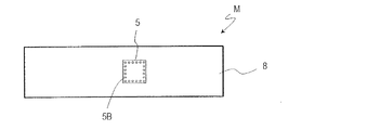
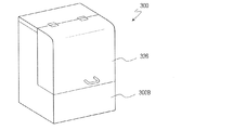
図13Aは、本開示の実施形態によるソケットの一例を示す。図13Bは、図13Aに示すソケット100aの側面図である。図13Aに示すように、ソケット100aは、概略的には、モジュールが載せられるモジュール設置部112が設けられた第1基材110と、第1基材110に結合可能に構成された第2基材150と、第2基材150を第1基材110に固定する係合部とを有している。
図20A〜図22を参照して、ソケットの変形例を説明する。
図23を参照して、本開示の実施形態による画像形成システムの構成例および動作を説明する。
これまでの説明では、モジュール設置部に直接載せられたモジュールを第1基材と第2基材とで挟むことによりモジュールが固定される構成を例示した。しかしながら、以下に説明するように、モジュールMを載せる部分が第1基材から取り外し可能であってもよい。
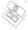
次に、図29〜図36を参照して、上述のアダプタ200の組み立てに適用可能な組立治具の構成と動作の一例を説明する。
イメージセンサ4は、CCDイメージセンサに限定されず、CMOS(Complementary Metal-Oxide Semiconductor)イメージセンサ、または、その他のイメージセンサ(一例として、後述する光電変換膜積層型イメージセンサ)であってもよい。CCDイメージセンサおよびCMOSイメージセンサは、表面照射型または裏面照射型のいずれであってもよい。以下、イメージセンサの素子構造と、イメージセンサのフォトダイオードに入射する光の関係を説明する。
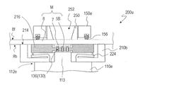
100u 被写体ユニット
110、110b、110c、110e 第1基材
112、112e モジュール設置部
113 突出部 114 平坦部
116 突出部
124、124c 突出部
130 電気接続部
150、150d、150e 第2基材
152、152e 開口部
156 押圧部
190 爪
200 アダプタ
200u 被写体ユニット
210 支持プレート
212s 支持面
214 平坦部
216 上部プレート
222 開口部
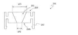
250 抑え具
252 開口部
250f 抑え具250の表面
250b 抑え具250の裏面
290 爪
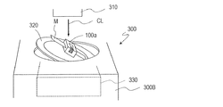
300 画像取得装置
310 光源
320、320b ステージ
330 ステージ駆動機構
400 画像処理装置
500 組立治具
510 底板
513 突出部
514 支持プレート保持部
518 壁部
550 フラップ
552 開口部
1000 画像形成システム
Claims (10)
- 撮像素子と被写体を含むモジュールが載せられるモジュール設置部および前記撮像素子と外部装置とを電気的に接続する電気接続部を含む第1基材と、
開口部を含む第2基材と、
前記第1基材と前記第2基材とが前記モジュール設置部に載せられた前記モジュールを挟んだ条件で、前記第1基材と前記第2基材とを係合する係合部とを備え、
前記第1基材と前記第2基材とが前記モジュール設置部に載せられた前記モジュールを挟んだ条件で、前記係合部が前記第1基材と前記第2基材とを係合したとき、前記電気接続部は前記撮像素子と電気的に接続され、前記被写体は前記開口部を通過した光源からの照明光を受光し、
前記電気接続部は、前記第1基材のモジュール設置部が設けられた面と反対の面に複数の底面電極を有する、
ソケット。 - 前記第1基材および前記第2基材はポリエーテルイミドまたはポリカーボネートが用いられる領域を含み、前記領域は前記モジュールに接する、
請求項1に記載のソケット。 - 前記モジュール設置部は、前記撮像素子を受け入れる凹部を有する、
請求項1または2に記載のソケット。 - 前記モジュール設置部は、前記モジュールの設置方向を示すマーカーを含む、
請求項3に記載のソケット。 - 前記モジュール設置部は、前記第1基材から着脱可能である、
請求項1または2に記載のソケット。 - 前記第2基材は、第1面と前記第1面と反対の面である第2面とを有し、
前記第1面は、前記第1基材と前記第2基材とが前記モジュール設置部に載せられた前記モジュールを挟んだ条件で、前記第1基材のモジュール設置部が設けられた面と対向し、
前記開口部の前記第1面上の面積は、前記開口部の前記第2面上の面積より小さく、
前記第1基材と前記第2基材とが前記モジュール設置部に載せられた前記モジュールを挟んだ条件で、前記係合部が前記第1基材と前記第2基材とを係合したとき、前記第1面と前記モジュールとの間の距離は、前記第2面と前記モジュールとの間の距離より小さい、
請求項1から5のいずれかに記載のソケット。 - 前記モジュールは透明プレートをさらに有し、
前記被写体は前記撮像素子と前記透明プレートとの間に位置する、
請求項1から6のいずれかに記載のソケット。 - 前記モジュール設置部は、前記第1基材と前記第2基材とが前記モジュール設置部に載せられた前記モジュールを挟んだ条件で、前記係合部が前記第1基材と前記第2基材とを係合したとき、前記透明プレートに接する平坦部を有する、
請求項7に記載のソケット。 - 前記ソケットは、第1押圧部と、前記第2基材に設けられた第2押圧部とをさらに含み、
前記第1基材と前記第2基材とが前記モジュール設置部に載せられた前記モジュールを挟んだ条件で、前記係合部が前記第1基材と前記第2基材とを係合したとき、前記第1押圧部は前記透明プレートの第1面を押圧し、前記第2押圧部は前記第1面と反対の面を押圧し、
前記第2押圧部の押圧力は、前記第1押圧部の押圧力よりも大きい、
請求項7または8に記載のソケット。 - 前記第1押圧部の押圧力および前記第2押圧部の押圧力は、前記透明プレートと前記撮像素子との間隔が所定の間隔よりも大きくならない押圧力である、
請求項9に記載のソケット。
Priority Applications (1)
| Application Number | Priority Date | Filing Date | Title |
|---|---|---|---|
| JP2015125970A JP6551835B2 (ja) | 2014-08-22 | 2015-06-23 | ソケット、アダプタ、および組立治具 |
Applications Claiming Priority (3)
| Application Number | Priority Date | Filing Date | Title |
|---|---|---|---|
| JP2014169405 | 2014-08-22 | ||
| JP2014169405 | 2014-08-22 | ||
| JP2015125970A JP6551835B2 (ja) | 2014-08-22 | 2015-06-23 | ソケット、アダプタ、および組立治具 |
Related Child Applications (2)
| Application Number | Title | Priority Date | Filing Date |
|---|---|---|---|
| JP2019060210A Division JP2019144564A (ja) | 2014-08-22 | 2019-03-27 | ソケット |
| JP2019115557A Division JP6739070B2 (ja) | 2014-08-22 | 2019-06-21 | 組立治具 |
Publications (2)
| Publication Number | Publication Date |
|---|---|
| JP2016045489A JP2016045489A (ja) | 2016-04-04 |
| JP6551835B2 true JP6551835B2 (ja) | 2019-07-31 |
Family
ID=53800905
Family Applications (3)
| Application Number | Title | Priority Date | Filing Date |
|---|---|---|---|
| JP2015125970A Expired - Fee Related JP6551835B2 (ja) | 2014-08-22 | 2015-06-23 | ソケット、アダプタ、および組立治具 |
| JP2019060210A Pending JP2019144564A (ja) | 2014-08-22 | 2019-03-27 | ソケット |
| JP2019115557A Expired - Fee Related JP6739070B2 (ja) | 2014-08-22 | 2019-06-21 | 組立治具 |
Family Applications After (2)
| Application Number | Title | Priority Date | Filing Date |
|---|---|---|---|
| JP2019060210A Pending JP2019144564A (ja) | 2014-08-22 | 2019-03-27 | ソケット |
| JP2019115557A Expired - Fee Related JP6739070B2 (ja) | 2014-08-22 | 2019-06-21 | 組立治具 |
Country Status (4)
| Country | Link |
|---|---|
| US (2) | US9799992B2 (ja) |
| EP (1) | EP2988156A3 (ja) |
| JP (3) | JP6551835B2 (ja) |
| CN (1) | CN105388606B (ja) |
Families Citing this family (20)
| Publication number | Priority date | Publication date | Assignee | Title |
|---|---|---|---|---|
| US10055062B2 (en) * | 2016-03-29 | 2018-08-21 | Microsoft Technology Licensing, Llc | Pressure sensing display |
| JP6750033B2 (ja) * | 2016-04-08 | 2020-09-02 | アレンティック マイクロサイエンス インコーポレイテッド | 顕微鏡検査のための試料処理 |
| CN107443465B (zh) * | 2017-09-12 | 2018-11-09 | 浙江中建路桥设备有限公司 | 一种桥梁建筑设备 |
| CN107425390B (zh) * | 2017-09-20 | 2023-10-10 | 黄山市振亿电子有限公司 | 整流桥电极与接线端子的装配夹具及其装配方法 |
| US12529094B2 (en) | 2018-12-10 | 2026-01-20 | 10X Genomics, Inc. | Imaging system hardware |
| WO2020123316A2 (en) | 2018-12-10 | 2020-06-18 | 10X Genomics, Inc. | Methods for determining a location of a biological analyte in a biological sample |
| US12405264B2 (en) | 2020-01-17 | 2025-09-02 | 10X Genomics, Inc. | Electrophoretic system and method for analyte capture |
| AU2021224860A1 (en) * | 2020-02-21 | 2022-09-15 | 10X Genomics, Inc. | Compositions, methods and systems for sample processing |
| WO2021174368A1 (en) * | 2020-03-06 | 2021-09-10 | Alentic Microscience Inc. | Portable imaging device |
| US12416603B2 (en) | 2020-05-19 | 2025-09-16 | 10X Genomics, Inc. | Electrophoresis cassettes and instrumentation |
| WO2021252747A1 (en) | 2020-06-10 | 2021-12-16 | 1Ox Genomics, Inc. | Fluid delivery methods |
| CN116472116A (zh) * | 2020-06-10 | 2023-07-21 | 10X基因组学有限公司 | 流体输送方法 |
| KR102844432B1 (ko) * | 2020-08-24 | 2025-08-11 | 삼성디스플레이 주식회사 | 표시 패널 검사용 지그 |
| CN112268181B (zh) * | 2020-10-28 | 2022-08-16 | 广东嘀嗒酷显柔性显示技术股份有限公司 | 一种可升降摄像模块及显示装置 |
| EP4421491A3 (en) | 2021-02-19 | 2024-11-27 | 10X Genomics, Inc. | Method of using a modular assay support device |
| US12553805B2 (en) | 2021-08-02 | 2026-02-17 | 10X Genomics, Inc. | Methods of preserving a biological sample |
| USD1064308S1 (en) | 2021-09-17 | 2025-02-25 | 10X Genomics, Inc. | Sample handling device |
| CN114589657A (zh) * | 2022-05-09 | 2022-06-07 | 立臻精密智造(昆山)有限公司 | 一种拆装装置 |
| US20240044754A1 (en) * | 2022-06-03 | 2024-02-08 | 10X Genomics, Inc. | Methods, systems, and devices for sample interface |
| CN117564979B (zh) * | 2024-01-17 | 2024-04-19 | 吉林省众汇净化工程有限公司 | 一种净化彩钢板的拆装定位夹具 |
Family Cites Families (18)
| Publication number | Priority date | Publication date | Assignee | Title |
|---|---|---|---|---|
| JPS5422471U (ja) * | 1977-07-15 | 1979-02-14 | ||
| JPS62137037A (ja) | 1985-12-11 | 1987-06-19 | 株式会社東芝 | X線撮影装置 |
| JP3120340B2 (ja) * | 1990-12-17 | 2000-12-25 | 株式会社パイオラックス | 蓋の開閉装置 |
| US5414556A (en) * | 1993-03-29 | 1995-05-09 | Focht; Daniel C. | Securing and locking assembly for live cell chambers |
| EP1171761B8 (en) | 1999-04-20 | 2009-02-25 | Dako Denmark A/S | Fluid exchange in a chamber on a microscope slide |
| CA2434604C (en) * | 2001-02-12 | 2010-09-28 | Immunivest Corporation | Cartridge for containing a specimen sample for optical analysis |
| JP3805649B2 (ja) * | 2001-06-14 | 2006-08-02 | シャープ株式会社 | 半導体検査装置 |
| JP4038070B2 (ja) * | 2002-04-24 | 2008-01-23 | 富士フイルム株式会社 | 固体撮像素子とその製造方法及び固定方法、及び撮像装置 |
| EP1527330A1 (en) * | 2002-08-06 | 2005-05-04 | The Regents of the University of California | Tear film osmometry |
| US7106526B2 (en) * | 2004-04-21 | 2006-09-12 | Matsushita Electric Industrial Co., Ltd. | Thin imaging apparatus, a thin camera, and an imaging method |
| JP2006337119A (ja) * | 2005-05-31 | 2006-12-14 | Seiko Epson Corp | 電子部品検査用治具 |
| US7262615B2 (en) * | 2005-10-31 | 2007-08-28 | Freescale Semiconductor, Inc. | Method and apparatus for testing a semiconductor structure having top-side and bottom-side connections |
| US8519358B2 (en) * | 2008-02-05 | 2013-08-27 | Pocared Diagnostics Ltd. | System for conducting the identification of bacteria in biological samples |
| TWI338601B (en) | 2008-11-24 | 2011-03-11 | Inventec Appliances Corp | Automatic assembly fixture |
| US9041790B2 (en) | 2009-10-28 | 2015-05-26 | Alentic Microscience Inc. | Microscopy imaging |
| JP2011108788A (ja) * | 2009-11-16 | 2011-06-02 | Yamaha Corp | 固体撮像素子検査用ソケット |
| JP2012229923A (ja) * | 2011-04-25 | 2012-11-22 | Micronics Japan Co Ltd | 電気的接続装置 |
| CN102857680B (zh) * | 2012-08-29 | 2016-02-24 | 惠州Tcl移动通信有限公司 | 摄像组件及配备有该摄像组件的电子设备 |
-
2015
- 2015-06-23 JP JP2015125970A patent/JP6551835B2/ja not_active Expired - Fee Related
- 2015-08-10 CN CN201510487437.7A patent/CN105388606B/zh not_active Expired - Fee Related
- 2015-08-11 US US14/823,659 patent/US9799992B2/en not_active Expired - Fee Related
- 2015-08-12 EP EP15180724.5A patent/EP2988156A3/en not_active Withdrawn
-
2017
- 2017-09-21 US US15/711,173 patent/US10256572B2/en not_active Expired - Fee Related
-
2019
- 2019-03-27 JP JP2019060210A patent/JP2019144564A/ja active Pending
- 2019-06-21 JP JP2019115557A patent/JP6739070B2/ja not_active Expired - Fee Related
Also Published As
| Publication number | Publication date |
|---|---|
| EP2988156A2 (en) | 2016-02-24 |
| JP6739070B2 (ja) | 2020-08-12 |
| CN105388606A (zh) | 2016-03-09 |
| JP2016045489A (ja) | 2016-04-04 |
| US20180019546A1 (en) | 2018-01-18 |
| US20160056577A1 (en) | 2016-02-25 |
| US10256572B2 (en) | 2019-04-09 |
| JP2019144564A (ja) | 2019-08-29 |
| CN105388606B (zh) | 2020-07-17 |
| US9799992B2 (en) | 2017-10-24 |
| JP2019174836A (ja) | 2019-10-10 |
| EP2988156A3 (en) | 2016-03-23 |
Similar Documents
| Publication | Publication Date | Title |
|---|---|---|
| JP6551835B2 (ja) | ソケット、アダプタ、および組立治具 | |
| DE112010005629B4 (de) | Kameramodul und Verfahren zum optischen Ausrichten eines Bildgebers mit einem Objektiv eines Kameramoduls | |
| CN102278941B (zh) | 测试装置 | |
| US10805596B2 (en) | Stereoscopic imaging sensor apparatus and method for fabricating pairs of image sensors used in stereoscopic imaging | |
| US20030030721A1 (en) | Digital camera, imaging device and method for digital imaging | |
| CN105764420A (zh) | 精确自动对准的ct检测器传感器 | |
| CN100345021C (zh) | 显微镜以及试样观察方法 | |
| WO2016067508A1 (ja) | 画像形成システム、画像形成方法、撮像素子、およびプログラム | |
| EP2094000A2 (de) | Bilderfassungsvorrichtung einer Kamera | |
| US11340441B2 (en) | Microscope made with CMOS camera(s) | |
| CN105829867A (zh) | 图像取得装置、图像形成系统和图像形成方法 | |
| JPS61203404A (ja) | Ccd撮像器にフイルタを取付ける方法 | |
| US20170146790A1 (en) | Image acquisition device and image formation system | |
| WO2016084309A1 (ja) | 電子プレパラート、固体撮像素子、電子プレパラート組み立てセット、および電子プレパラートの組み立て方法 | |
| JP6545457B2 (ja) | プレパラート、透明プレート、プレパラートの作製方法、スライドガラス、画像撮影装置、画像撮影方法、プレパラート作製装置、およびプレパラート部品セット | |
| CN106483338A (zh) | 图像输出装置、图像发送装置、图像接收装置、图像输出方法 | |
| KR20210148026A (ko) | 카메라 모듈 검사장치 | |
| JP2015047249A (ja) | 内視鏡 | |
| KR100663196B1 (ko) | 일체형 프로브 마운트 및 이를 포함하는 현미경 | |
| JP4005373B2 (ja) | 固体撮像装置 | |
| KR20130051841A (ko) | 얼라인 장치 및 그 방법 | |
| TWI282404B (en) | Line width measuring apparatus | |
| Cheng | Spatio-temporally Multiplexed Multiphoton Calcium Imaging for Monitoring Neuronal Networks In Vivo | |
| TWM274639U (en) | Multi-angle optical inspecting apparatus for IC packaging devices |
Legal Events
| Date | Code | Title | Description |
|---|---|---|---|
| A621 | Written request for application examination |
Free format text: JAPANESE INTERMEDIATE CODE: A621 Effective date: 20180525 |
|
| A977 | Report on retrieval |
Free format text: JAPANESE INTERMEDIATE CODE: A971007 Effective date: 20190118 |
|
| A131 | Notification of reasons for refusal |
Free format text: JAPANESE INTERMEDIATE CODE: A131 Effective date: 20190129 |
|
| A521 | Request for written amendment filed |
Free format text: JAPANESE INTERMEDIATE CODE: A523 Effective date: 20190327 |
|
| TRDD | Decision of grant or rejection written | ||
| A01 | Written decision to grant a patent or to grant a registration (utility model) |
Free format text: JAPANESE INTERMEDIATE CODE: A01 Effective date: 20190611 |
|
| A61 | First payment of annual fees (during grant procedure) |
Free format text: JAPANESE INTERMEDIATE CODE: A61 Effective date: 20190621 |
|
| R151 | Written notification of patent or utility model registration |
Ref document number: 6551835 Country of ref document: JP Free format text: JAPANESE INTERMEDIATE CODE: R151 |
|
| LAPS | Cancellation because of no payment of annual fees |