JP6526345B1 - Filter structure for PIM measurement - Google Patents
Filter structure for PIM measurement Download PDFInfo
- Publication number
- JP6526345B1 JP6526345B1 JP2018540762A JP2018540762A JP6526345B1 JP 6526345 B1 JP6526345 B1 JP 6526345B1 JP 2018540762 A JP2018540762 A JP 2018540762A JP 2018540762 A JP2018540762 A JP 2018540762A JP 6526345 B1 JP6526345 B1 JP 6526345B1
- Authority
- JP
- Japan
- Prior art keywords
- port
- filter
- duplexer
- cover
- pim
- Prior art date
- Legal status (The legal status is an assumption and is not a legal conclusion. Google has not performed a legal analysis and makes no representation as to the accuracy of the status listed.)
- Active
Links
Images


Classifications
-
- H—ELECTRICITY
- H01—ELECTRIC ELEMENTS
- H01P—WAVEGUIDES; RESONATORS, LINES, OR OTHER DEVICES OF THE WAVEGUIDE TYPE
- H01P1/00—Auxiliary devices
- H01P1/20—Frequency-selective devices, e.g. filters
- H01P1/213—Frequency-selective devices, e.g. filters combining or separating two or more different frequencies
- H01P1/2136—Frequency-selective devices, e.g. filters combining or separating two or more different frequencies using comb or interdigital filters; using cascaded coaxial cavities
-
- H—ELECTRICITY
- H01—ELECTRIC ELEMENTS
- H01P—WAVEGUIDES; RESONATORS, LINES, OR OTHER DEVICES OF THE WAVEGUIDE TYPE
- H01P1/00—Auxiliary devices
- H01P1/20—Frequency-selective devices, e.g. filters
- H01P1/201—Filters for transverse electromagnetic waves
- H01P1/205—Comb or interdigital filters; Cascaded coaxial cavities
- H01P1/2053—Comb or interdigital filters; Cascaded coaxial cavities the coaxial cavity resonators being disposed parall to each other
-
- G—PHYSICS
- G01—MEASURING; TESTING
- G01R—MEASURING ELECTRIC VARIABLES; MEASURING MAGNETIC VARIABLES
- G01R1/00—Details of instruments or arrangements of the types included in groups G01R5/00 - G01R13/00 and G01R31/00
- G01R1/20—Modifications of basic electric elements for use in electric measuring instruments; Structural combinations of such elements with such instruments
- G01R1/24—Transmission-line, e.g. waveguide, measuring sections, e.g. slotted section
-
- H—ELECTRICITY
- H01—ELECTRIC ELEMENTS
- H01P—WAVEGUIDES; RESONATORS, LINES, OR OTHER DEVICES OF THE WAVEGUIDE TYPE
- H01P1/00—Auxiliary devices
- H01P1/20—Frequency-selective devices, e.g. filters
- H01P1/207—Hollow waveguide filters
- H01P1/208—Cascaded cavities; Cascaded resonators inside a hollow waveguide structure
-
- H—ELECTRICITY
- H01—ELECTRIC ELEMENTS
- H01P—WAVEGUIDES; RESONATORS, LINES, OR OTHER DEVICES OF THE WAVEGUIDE TYPE
- H01P5/00—Coupling devices of the waveguide type
- H01P5/12—Coupling devices having more than two ports
- H01P5/16—Conjugate devices, i.e. devices having at least one port decoupled from one other port
-
- H—ELECTRICITY
- H01—ELECTRIC ELEMENTS
- H01P—WAVEGUIDES; RESONATORS, LINES, OR OTHER DEVICES OF THE WAVEGUIDE TYPE
- H01P7/00—Resonators of the waveguide type
- H01P7/04—Coaxial resonators
Abstract
PIM(Passive Inter Modulation:パッシブ相互変調)テストベンチは、第1のフィルタを介して第3のポートに接続された第1のポートと、第2のフィルタを介して前記第3のポートに接続された第2のポートとを有する第1のデュプレクサを含む。第1のポートは、第1の周波数および第2の周波数でRF信号を供給する信号源によって供給されている。スペクトルアナライザは、第2のポートに接続されている。DUT(Device under Test:被試験デバイス)は、前記第3のポートと第2のデュプレクサの第3のポートとの間に接続されている。第2のデュプレクサの第1のポートおよび第2のポートの各々は、PIM最適化された負荷および/または標準負荷に接続されている。第2のデュプレクサは、好ましくは第1のデュプレクサと同一である。自己相互変調を最小化するために、少なくとも前記第1のデュプレクサは、少なくとも1つのフィルタコンポーネントと、金属性のハウジングとを含み、前記ハウジングはさらに、モノリシックな金属性の本体と、如何なるガルバニック接触をも有することなく前記本体に容量的に結合された金属性のカバーとを含む。A PIM (Passive Inter Modulation) test bench is connected to a first port connected to a third port via a first filter and to the third port via a second filter. And a first duplexer having a second port. The first port is provided by a signal source that provides an RF signal at a first frequency and a second frequency. A spectrum analyzer is connected to the second port. A device under test (DUT) is connected between the third port and a third port of the second duplexer. Each of the first and second ports of the second duplexer is connected to the PIM optimized load and / or the standard load. The second duplexer is preferably identical to the first duplexer. In order to minimize self-intermodulation, at least the first duplexer includes at least one filter component and a metallic housing, which further includes a monolithic metallic body and any galvanic contacts. And a metallic cover capacitively coupled to the body without having any.
Description
発明の分野
本発明は、RF信号のPIM(Passive InterModulation:パッシブ相互変調、相互変調歪み)測定のためのフィルタ構造に関する。
FIELD OF THE INVENTION The present invention relates to a filter structure for PIM (Passive InterModulation) measurement of RF signals.
関連技術の説明
RF信号の相互変調は、通常、複数の周波数の組合せによって低電力レベルでも様々な相互変調積が生成される、増幅器またはミキサのような非線形デバイスにおける問題と呼ばれている。それぞれ異なる周波数の2つの正弦波信号の場合、相互変調積は、以下の周波数を有する:
fIM=|k1f1±k2f2|
k1およびk2は自然数であり、k1+k2は、相互変調積の次数である。
Description of the Related Art Intermodulation of RF signals is commonly referred to as a problem in non-linear devices such as amplifiers or mixers where the combination of multiple frequencies produces various intermodulation products even at low power levels. In the case of two sinusoidal signals, each of a different frequency, the intermodulation products have the following frequencies:
f IM = | k 1 f 1 ± k 2 f 2 |
k 1 and k 2 are natural numbers, and k 1 + k 2 is the order of intermodulation products.
しかしながら、実際には、ケーブルまたはフィルタのような通常は線形と呼ばれる受動コンポーネントでさえも相互変調積が発生することがある。これは「パッシブ相互変調」または「PIM」と呼ばれる。その原因は、磁性材料の使用であるか、または、ガルバニックRF接触不良である可能性がある。これらは、どちらかと言えば弱いソースであるので、PIMは、通常、半導体デバイスにおける相互変調積に比べてはるかに高い電力レベルでのみ明らかとなる。 However, in practice, intermodulation products can occur even with passive components, usually called linear, such as cables or filters. This is called "passive intermodulation" or "PIM". The cause may be the use of magnetic material or galvanic RF contact failure. Because these are rather weak sources, PIM is usually only apparent at much higher power levels than intermodulation products in semiconductor devices.
その影響によって、移動体通信システムにおいて重大な問題が引き起こされる可能性がある。例えば、2つの搬送波がLTE800のTX帯域の帯域エッジで送信される場合には、RX帯域に1つの相互変調積が位置することとなり、信号対雑音比を劣化させる追加的な歪みとして作用する。この歪みは、如何なる手段を用いてもフィルタリングすることができないので、システムの全てのコンポーネントによって生成される歪みをできるだけ小さくすることが重要である。このような理由から、移動体通信インフラストラクチャコンポーネントをPIMに関してテストすることが、製造プロセスにおいて重要な役割を果たしている。 The impact can cause serious problems in the mobile communication system. For example, if two carriers are transmitted at the band edge of the LTE 800 TX band, one intermodulation product will be located in the RX band, which acts as an additional distortion that degrades the signal to noise ratio. Since this distortion can not be filtered by any means, it is important to minimize the distortion generated by all components of the system. For these reasons, testing mobile communication infrastructure components for PIM plays an important role in the manufacturing process.
PIM測定の方法は標準化されており、例えばIEC62037−1に記載されている。第1の周波数または周波数範囲内の信号がDUT(device under test:被試験デバイス)に印加され、DUTによって生成された相互変調信号が第2の周波数または周波数範囲において測定される。このようなシステムの、測定の不確かさへの寄与は、2つの搬送波信号の電力の精度の正確性と、PIMテストベンチおよびPIM最適化された負荷の自己相互変調の正確性の制限である。3dB未満の許容可能な測定誤差を設けるためには、テストベンチの相互変調と、被試験デバイスの相互変調との間に少なくとも10dBの差が必要である。多数の移動体通信インフラストラクチャコンポーネントは、−165dBcで仕様が定められているので、−175dBcよりも良好な自己相互変調を有するテストデバイスを有することが必要であろう。残念なことに、そのようなテストデバイスは、現在のところ市販されていない。 The method of PIM measurement is standardized and described in, for example, IEC 62037-1. A signal within a first frequency or frequency range is applied to a DUT (device under test), and an intermodulation signal generated by the DUT is measured at a second frequency or frequency range. The contribution of such a system to measurement uncertainty is the accuracy of the power accuracy of the two carrier signals and the limitation of the self intermodulation accuracy of the PIM test bench and PIM optimized loads. In order to provide an acceptable measurement error of less than 3 dB, a difference of at least 10 dB is required between the intermodulation of the test bench and the intermodulation of the device under test. Since many mobile communication infrastructure components are specified at -165 dBc, it will be necessary to have test devices with self-intermodulation better than -175 dBc. Unfortunately, such test devices are not currently commercially available.
PIMを緩和するための方法は、米国特許第9306261号明細書(US 9,306,261 B2)に開示されている。この方法は、強磁性の導電性金属によって引き起こされるPIMに限定されている。 A method to mitigate PIM is disclosed in US Pat. No. 9,306,261 (US 9,306,261 B2). This method is limited to PIMs caused by ferromagnetic conductive metals.
PIM測定デバイスの最も重要なコンポーネントは、DUT(Device Under Test:被試験デバイス)によって生成されて反射されたPIMを、電力レベルが測定されうる別の出力ポートへと分割するデュプレクサである。フィルタ選択性が、受信機におけるPIMの生成、または、増幅器で生成されたPIMのテストポートへの送信のような如何なる二次的な影響をも回避するために十分であると仮定すると、測定デバイスの残留PIMは、主としてデュプレクサ自身のパッシブ相互変調によって引き起こされることとなる。 The most important component of a PIM measurement device is a duplexer that splits the PIM generated and reflected by the DUT (Device Under Test) into another output port where power levels can be measured. Assuming that the filter selectivity is sufficient to avoid any secondary effects such as generation of PIM at the receiver or transmission of amplifier generated PIM to the test port, the measurement device The residual PIM of will be caused mainly by the passive intermodulation of the duplexer itself.
デュプレクサのために使用されうるコムラインフィルタは、米国特許第4307357号明細書(US 4,307,357)号に開示されている。実際に、このようなフィルタの自己相互変調は、最新の通信コンポーネントのPIMよりも高い。 A combline filter that can be used for a duplexer is disclosed in US Pat. No. 4,307,357 (US Pat. No. 4,307,357). In fact, the self intermodulation of such filters is higher than the PIM of modern communication components.
米国特許第8742869号明細書(US 8,742,869 B2)は、低PIMコンデンサを有する改善されたダイプレクサを開示している。このダイプレクサは、自己相互変調を−156dBcまで改善するために役立つが、この−156dBcという値は、要求される値から依然として約20dBだけ離れている。 U.S. Pat. No. 8,742,869 (US 8,742,869 B2) discloses an improved diplexer having a low PIM capacitor. Although this diplexer helps to improve self intermodulation to -156 dBc, this value of -156 dBc is still about 20 dB away from the required value.
米国特許第8362855号明細書(US 8,362,855 B2)は、PIMが低減されたフィルタを開示している。このフィルタは、ハウジングカバーとハウジング本体との間のガルバニック接触を改善するために特別なボルト締め技術を使用している。
国際公開第93/01625号(WO 93/01625)は、PIMが低減されたコムラインダイプレクサを開示しており、ここでは、共振器間を分離する複数の壁が、フィルタの蓋部の手前で終端されている。
独国特許出願公開第102014011514号明細書(DE 10 2014 011 514 A1)は、薄いシートメタルから形成された、基地局のアンテナのための、PIMが低減されたハウジングを開示している。プレスナットが不正確に配置される問題を回避するために、容量性カップリングが設けられている。
U.S. Pat. No. 8,362,855 B2 discloses a PIM reduced filter. This filter uses a special bolting technique to improve the galvanic contact between the housing cover and the housing body.
WO 93/01625 (WO 93/01625) discloses a PIM reduced combline diplexer, in which the walls separating the resonators are in front of the lid of the filter It is terminated.
DE 10 2014 0115 14 (DE 10 2014 011 514 A1) discloses a PIM-reduced housing for a base station antenna, made of thin sheet metal. A capacitive coupling is provided to avoid problems with the press nut being incorrectly positioned.
発明の概要
本発明によって解決しようとする課題は、改善されたPIMテストベンチと、改善されたデュプレクサとを提供することである。さらなる態様は、低PIMフィルタを改善することに関する。好ましくは、PIMテストベンチおよびデュプレクサは、−175dBcよりも良好な自己相互変調を有する。
SUMMARY OF THE INVENTION The problem to be solved by the present invention is to provide an improved PIM test bench and an improved duplexer. A further aspect relates to improving the low PIM filter. Preferably, PIM test benches and duplexers have better than -175 dBc self intermodulation.
上記の課題の解決策は、独立請求項に記載されている。従属請求項は、本発明のさらなる改善に関する。 The solution to the above problem is described in the independent claims. The dependent claims relate to further improvements of the invention.
長期にわたる一連のテストおよび測定により、フィルタ構造の、特にデュプレクサのPIMが、ハウジング本体と、デュプレクサを囲っているカバーとの間のガルバニック接触によって依然として制限されていることが示された。 A series of tests and measurements over time showed that the PIM of the filter structure, in particular the duplexer, is still limited by the galvanic contact between the housing body and the cover surrounding the duplexer.
フィルタハウジング本体の頂部は、決して完全には平坦ではない。したがって、ハウジング本体とカバーとの間の接触領域全体にわたって十分な接触圧力を提供することは非常に困難である。組み立てられた状態では、フィルタハウジング本体の材料の内部における張力の解放に起因してわずかな動きが生じることがある。これは、時間と共に接触品質の変化をもたらす可能性がある。さらに、フィルタ構造を所望の周波数応答に同調させるために同調要素が必要である。 The top of the filter housing body is by no means completely flat. Thus, it is very difficult to provide sufficient contact pressure across the contact area between the housing body and the cover. In the assembled state, slight movement may occur due to the release of tension inside the material of the filter housing body. This can lead to changes in contact quality over time. Furthermore, a tuning element is required to tune the filter structure to the desired frequency response.
これらの要素も、通常、フィルタハウジング本体またはカバーとのガルバニック接触を有し、同調中の動きによって金属粒子がフィルタの内部に浸透する可能性がある。如何なるガルバニック接触も、酸化のような大気との化学反応に起因して自身の特性を変化させる可能性もある。輸送中の振動および衝撃が、フィルタ構造の内部のガルバニック接触を悪化させるおそれもある。これらのメカニズムによって長期安定性の問題が生じるおそれがある。しかしながら、たとえフィルタ構造が安定していたとしても、従来の設計によって達成可能な残留PIMは、典型的に、フィルタ帯域幅全体にわたって+43dBmの搬送波電力において−170dBc程度に過ぎず、このような値は、−165dBcよりも良好なコンポーネントをテストするためには不十分である。 These elements also typically have galvanic contact with the filter housing body or cover, and movement during tuning can allow metal particles to penetrate the interior of the filter. Any galvanic contact can change its properties due to chemical reactions with the atmosphere such as oxidation. Vibration and shock during transport can also degrade the galvanic contact inside the filter structure. These mechanisms can cause long-term stability problems. However, even if the filter structure is stable, the residual PIM achievable by conventional designs is typically only about -170 dBc at +43 dBm carrier power across the filter bandwidth, and such values are Insufficient to test components better than -165 dBc.
したがって、好ましい実施形態では、従来技術の教示とは反対に、ハウジング本体とカバーとの間の如何なるガルバニック接触をも回避する必要がある。さらに、ハウジング本体とカバーとの間において低インピーダンスを提供するために、これらの間に強力な容量性カップリングを設けなければならない。 Thus, in a preferred embodiment, contrary to the teachings of the prior art, it is necessary to avoid any galvanic contact between the housing body and the cover. Furthermore, in order to provide low impedance between the housing body and the cover, a strong capacitive coupling must be provided between them.
デュプレクサは、好ましくはモノリシックなハウジング本体を有し、ハウジング本体は、最も好ましくは、アルミニウム、または、任意の他の適切な材料からフライス加工によって形成されている。同軸共振器ロッドを設けることができ、この同軸共振器ロッドをハウジング本体の一部とすることができる。アルミニウム製のカバーは、好ましくは、如何なるガルバニック接触をも有することなくフィルタハウジング本体に容量的に結合されている。このことは、誘電体層を設けることによって達成することができ、この誘電体層は、カバーおよび/または本体のコーティングとすることができる。好ましくは、カバーは、少なくともハウジング本体の方を向いた面またはカバーの面全体に誘電体層を有する。本体が、少なくともハウジングカバーの方を向いた面または本体の面全体に誘電体層を有すると、さらに好ましい。 The duplexer has a preferably monolithic housing body, which is most preferably formed by milling from aluminum or any other suitable material. A coaxial resonator rod can be provided, which can be part of the housing body. An aluminum cover is preferably capacitively coupled to the filter housing body without any galvanic contact. This can be achieved by providing a dielectric layer, which can be a coating on the cover and / or the body. Preferably, the cover has a dielectric layer at least on the side facing the housing body or on the whole side of the cover. It is further preferred that the body has a dielectric layer at least on the side facing the housing cover or on the whole side of the body.
本明細書において言及される誘電体層は、好ましくは2μm〜200μmの範囲内の厚さを有する。最も好ましくは10μm〜30μmの間の範囲である。この層は、陽極酸化層、酸化物、任意のセラミック材料、塗料、プラスチックフィルム、ポリマー材料、または、これらの任意の組合せを含むことができる。 The dielectric layers mentioned herein preferably have a thickness in the range of 2 μm to 200 μm. Most preferably, it is in the range of 10 μm to 30 μm. This layer can comprise an anodized layer, an oxide, any ceramic material, a paint, a plastic film, a polymer material, or any combination thereof.
カバーは、好ましくはガラス繊維強化プラスチック製のねじによってハウジング本体に固定されている。これによって、ねじによるカバーと本体との間の如何なるガルバニック接触も回避される。 The cover is preferably fixed to the housing body by means of screws made of glass fiber reinforced plastic. This avoids any galvanic contact between the screw cover and the body.
フィルタの入力カップリングおよび出力カップリングは、容量性とすることができる。これらのカップリングは、好ましくは、それぞれの外部コネクタのためのモノリシックな内部導体の一部である。共振器のための同調要素は、好ましくは酸化アルミニウムから形成されている。全ての共振器間カップリングは、好ましくはアルミニウムから形成されており、好ましくはカバーと同じ方法でコーティングされている。結果として、カバーと同調要素とは、これらの間の静電容量のみによって結合されることとなる。ガルバニック接触は存在しない。同調要素を固定するナットのような固定要素も、好ましくは、同調要素およびカバーのいずれにもガルバニック接触しないように絶縁されている。固定ナットと同調要素との間に誘電性のスリーブを設けることができる。さらに、少なくとも1つの同調要素は、カバーとの如何なるガルバニック接触をも防止するために、自身の外側に誘電体層を有することができる。概して好ましくは、フィルタの全ての要素は、モノリシックな部品であり、要素間の接合部は、ガルバニック接触を回避するために誘電体層を間に有する。好ましくは、複数のモノリシックな要素の間の全ての静電容量は、線形性への悪影響を有することなく、所望の周波数範囲内でのガルバニック接触に代わる適切な置換えとなるために十分に低いインピーダンスを提供するように、ガルバニック接触を有することなく容量性カップリングを提供するように設計されている。 The filter's input coupling and output coupling can be capacitive. These couplings are preferably part of monolithic inner conductors for the respective outer connectors. The tuning element for the resonator is preferably made of aluminum oxide. All interresonator couplings are preferably made of aluminum and are preferably coated in the same manner as the cover. As a result, the cover and the tuning element will be coupled only by the capacitance between them. There is no galvanic contact. A locking element, such as a nut, for locking the tuning element is also preferably insulated so as not to have galvanic contact with either of the tuning element and the cover. A dielectric sleeve can be provided between the locking nut and the tuning element. Additionally, the at least one tuning element can have a dielectric layer outside of it to prevent any galvanic contact with the cover. Generally preferably, all elements of the filter are monolithic parts, and the joints between the elements have dielectric layers in between to avoid galvanic contact. Preferably, all capacitances between the plurality of monolithic elements have an impedance low enough to be a suitable replacement for galvanic contact in the desired frequency range without having an adverse effect on linearity. To provide a capacitive coupling without galvanic contact.
カバーによって覆われた本体のスクリーニング効果が、環境から捕捉されたランダムな信号による誤った測定結果を回避するためには十分ではないことが、テストによって示された。遮蔽性を改善するために、フィルタカバーの上に、キャップとして形成される追加的なシールドを取り付けることができ、この追加的なシールドは、好ましくはベリリウム銅から形成される接触ストリップを介してフィルタハウジング本体に接続されている。実際には、これはガルバニック接触であるが、フィルタ構造の外側にあり、したがって搬送波信号から強力に切り離されている。この接触によって生成されるPIMも、PIM出力ポートから切り離されている。したがって、この追加的なキャップは、デュプレクサの残留PIMに対して顕著な影響を及ぼすことなく110dBよりも良好で十分なスクリーニング効果を達成するための優れた妥協策である。デュプレクサのポートコネクタの外部導体も、フィルタハウジング本体に直接的に接触することができる。ここの接触面積は小さいので、凹凸がフィルタハウジング本体内での張力の解放と同様に二次的な役割を果たしている。したがって、ここではガルバニック接触を許容することが可能である。 Tests have shown that the screening effect of the body covered by the cover is not sufficient to avoid false measurements due to random signals captured from the environment. In order to improve the shielding, an additional shield, which is formed as a cap, can be mounted on the filter cover, which is preferably filtered through a contact strip formed of beryllium copper. It is connected to the housing body. In practice, this is a galvanic contact, but outside the filter structure and thus strongly decoupled from the carrier signal. The PIM generated by this contact is also decoupled from the PIM output port. Thus, this additional cap is an excellent compromise to achieve better than 110 dB and sufficient screening effect without significant impact on the residual PIM of the duplexer. The outer conductor of the port connector of the duplexer can also be in direct contact with the filter housing body. Since the contact area here is small, the asperities play a secondary role as well as the release of tension in the filter housing body. Thus, it is possible here to allow galvanic contact.
本提示の設計の特徴の1つの欠点について言及しなければならない。非接触のフィルタカバーであるが故に、達成可能な入力ポートのアイソレーションが制限されているのである。2つのフィルタ経路の間のリッジにおけるハウジング本体とカバーとの間の静電容量は、グラウンドに対するブロックキャパシタンスのように作用し、周波数範囲に依存する経路間のアイソレーションが制限されたローパス挙動を示す。この理由から、本明細書で提示されるデュプレクサは、わずか60dBのポートアイソレーションで設計されてきた。デュプレクサの第1のポートおよび第2のポートに接続される追加的なフィルタを用いることにより、PIM測定デバイスに対して望まれる約120dBのアイソレーションが達成される。PIMに関するこれらの追加フィルタの要件は非常に低いので、市販の標準的な製品を使用することができる。 One drawback of the design features of the present presentation has to be mentioned. Due to the non-contacting filter cover, the achievable isolation of the input port is limited. The capacitance between the housing body and the cover at the ridge between the two filter paths acts like a block capacitance to ground and exhibits low pass behavior with limited isolation between the frequency range dependent paths . For this reason, the duplexers presented herein have been designed with only 60 dB port isolation. By using additional filters connected to the first and second ports of the duplexer, the isolation of about 120 dB desired for the PIM measurement device is achieved. The requirements for these additional filters for PIM are so low that standard commercial products can be used.
さらなる実施形態では、負荷が改善されており、これによってテストベンチの自己相互変調がさらに低減されている。ここでは、テストベンチは、テストベンチのデュプレクサの第3のポートに接続された第2のデュプレクサによって終端されている。第2のデュプレクサのTX出力部は、PIM最適化された負荷に接続されており、RX出力部は、通常の50Ωの負荷によって終端されている。第2のデュプレクサの目的は、PIMに最適化された負荷によって生成されたPIM信号をブロックして、このPIM信号がPIMアナライザのテストポートに進行することができないようにすることである。第2のデュプレクサは、好ましくは上述したデュプレクサと同じ、容量的に結合されたカバーを有する。第2のデュプレクサは、最も好ましくは同一のデュプレクサである。 In a further embodiment, the loading is improved, which further reduces the self-intermodulation of the test bench. Here, the test bench is terminated by a second duplexer connected to the third port of the test bench duplexer. The TX output of the second duplexer is connected to the PIM optimized load and the RX output is terminated by a normal 50 Ω load. The purpose of the second duplexer is to block the PIM signal generated by the PIM optimized load so that it can not travel to the PIM analyzer's test port. The second duplexer preferably has the same capacitively coupled cover as the duplexer described above. The second duplexer is most preferably the same duplexer.
PIMアナライザのためのデュプレクサと、このようなデュプレクサを少なくとも1つ含むPIMテストベンチとは、低減された自己相互変調を提供し、したがって、フィルタ構造の内部に如何なるガルバニック接触も存在しないことに起因して、PIM測定値をより低いレベルにすることを可能にする。これにより、PIMの生成が最小化され、ガルバニック接触の長期安定性の問題が回避される。 The duplexer for the PIM analyzer and the PIM test bench comprising at least one such duplexer provide a reduced self-intermodulation and hence due to the absence of any galvanic contact inside the filter structure To allow PIM measurements to be at lower levels. This minimizes PIM generation and avoids the problem of long term stability of galvanic contacts.
本明細書に記載されたデュプレクサハウジングの基本的な概念は、デュプレクサに限定されているわけではなく、低PIMが要求される任意のフィルタまたは任意の電子コンポーネントのハウジングにさえも適用することもできる。基本的に、ハウジングは、好ましくは1つの部品から機械加工されたモノリシックな金属性の本体と、如何なるガルバニック接触をも有することなく本体に容量的に結合された金属製のカバーとを含む。好ましくは、カバーを覆うようにシールドが設けられている。シールドは、少なくとも1つの本体接触面を有することができ、本体接触面を介してシールドの少なくとも1つのシールド接触面とガルバニック接触している。カバーは、少なくともハウジング本体の方を向いた面またはカバーの面全体に誘電体層を有することができる。本体は、少なくともハウジングカバーの方を向いた面または本体の面全体に誘電体層を有することができる。好ましくは、本体は、カバーの本体結合面に一致するカバー結合面を有し、この場合、カバー結合面および本体結合面の少なくとも一方は、誘電体層を有することができる。誘電体層は、コーティング、酸化物層、および、ガルバニック層のうちの少なくとも1つを含むことができる。カバーは、絶縁材料を含む手段によって、好ましくは、ガラス繊維強化プラスチック製のねじ、ボルトまたはピンによってハウジング本体に固定されうる。 The basic concept of duplexer housing described herein is not limited to duplexers, but can also be applied to the housing of any filter or any electronic component where low PIM is required . Basically, the housing comprises a monolithic metallic body, preferably machined from one piece, and a metallic cover capacitively coupled to the body without any galvanic contact. Preferably, a shield is provided to cover the cover. The shield may have at least one body contact surface and is in galvanic contact with the at least one shield contact surface of the shield via the body contact surface. The cover may have a dielectric layer at least on the side facing the housing body or on the whole side of the cover. The body may have a dielectric layer at least on the side facing the housing cover or on the whole side of the body. Preferably, the body has a cover bonding surface that matches the body bonding surface of the cover, in which case at least one of the cover bonding surface and the body bonding surface can have a dielectric layer. The dielectric layer can include at least one of a coating, an oxide layer, and a galvanic layer. The cover may be fixed to the housing body by means of an insulating material, preferably by means of screws, bolts or pins made of glass fiber reinforced plastic.
好ましくは、同軸共振器ロッドのうちの少なくとも1つは、ハウジング本体の少なくとも一部である。フィルタがデュプレクサであると、好ましい。デュプレクサが、第1のバンドパスフィルタを介して第3のポートに接続された第1のポートと、第2のバンドパスフィルタを介して第3のポートに接続された第2のポートとを有すると、さらに好ましい。最も好ましくは、フィルタは、好ましくは、2つのトリプレットを利用した楕円6空洞型フィルタコンポーネントを含むデュプレクサである。 Good Mashiku, at least one of the coaxial resonators rod is at least a portion of the housing body. Preferably the filter is a duplexer. The duplexer has a first port connected to the third port via the first band pass filter and a second port connected to the third port via the second band pass filter. Then, it is more preferable. Most preferably, the filter is a duplexer, preferably including an elliptical six-cavity filter component utilizing two triplets.
本明細書におけるRF信号という用語は、任意の高周波信号、無線周波数信号、マイクロ波信号、または、ミリ波信号を指している。DUTという用語は、Device Under Test(被試験デバイス)を意味し、すなわち、テストベンチによってテストされる対象を意味する。フィルタまたはフィルタ構造という用語は、周波数選択性または方向選択性の電子コンポーネントに関する。フィルタの例は、ハイパスフィルタ、ローパスフィルタ、バンドパスフィルタ、または、方向性カプラである。フィルタコンポーネントは、フィルタにおいて使用される電子コンポーネントである。例として、インダクタ、コンデンサ、ならびに、誘電体共振器および共振性空洞を含む共振器がある。 The term RF signal herein refers to any high frequency signal, radio frequency signal, microwave signal or millimeter wave signal. The term DUT means Device Under Test, ie an object to be tested by the test bench. The term filter or filter structure relates to frequency or direction selective electronic components. Examples of filters are high pass filters, low pass filters, band pass filters or directional couplers. A filter component is an electronic component used in a filter. Examples include inductors, capacitors, and resonators including dielectric resonators and resonant cavities.
図面の説明
以下では本発明を、実施例に基づいて図面を参照しながら、一般的な発明概念を制限することなく一例として説明する。
DESCRIPTION OF THE DRAWINGS The invention will be described in the following by way of example and with reference to the drawings, without restricting the general inventive concept.
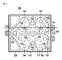
図1には、本発明による好ましい実施形態が示されている。図1は、PIM(Passive InterModulation:パッシブ相互変調、相互変調歪み)測定のために使用されうるデュプレクサのハウジング本体の上面図を示す。このデュプレクサを使用するPIMテストベンチの回路図が図5に示されている。図5では、フィルタは、参照符号100を有する。例示されているハウジング本体は、コムラインフィルタの一部である。第2のポートコネクタ732と第3のポートコネクタ733との間のRX経路と、第1のポートコネクタ731と第3のポートコネクタ733との間のTX経路とは、両方とも、それぞれの経路の阻止帯域において2つの伝送零点を形成することによってフィルタエッジの所要の急峻性を達成するために、2つのトリプレットを利用した楕円6空洞型フィルタを有する。これら2つの経路は、1つの共通のノードによって組み合わせられる。
A preferred embodiment according to the present invention is shown in FIG. FIG. 1 shows a top view of the housing body of a duplexer that may be used for PIM (Passive InterModulation) measurements. A schematic of a PIM test bench using this duplexer is shown in FIG. In FIG. 5 the filter has the
デュプレクサは、好ましくはモノリシックなハウジング本体700を有し、ハウジング本体700は、最も好ましくは、アルミニウム、または、任意の他の適切な導電性材料からフライス加工によって形成されている。ハウジングは、好ましくは、共振器ロッド740または共振器間カップリング742のようなフィルタコンポーネントを含む。ハウジングは、共振器空洞を形成することもできる。同軸共振器ロッド740は、好ましくはハウジング本体の一部である。好ましくはアルミニウムを含む、金属製のカバー780は、如何なるガルバニック接触をも有することなくフィルタハウジング本体700に容量的に結合されている。このことは、カバー780を薄い誘電体層でコーティングすることによって達成することができる。誘電体層は、好ましくは2μm〜200μmの範囲内の厚さを有する。最も好ましくは10μm〜30μmの間の範囲である。この層は、陽極酸化層、酸化物、任意のセラミック材料、塗料、プラスチックフィルム、ポリマー材料、または、これらの任意の組合せを含むことができる。追加的または代替的な形態では、ハウジング本体700が、または、カバーが取り付けられる少なくとも1つのカバー結合面710が、このような薄い誘電体層によってコーティングされる。カバー780は、好ましくはガラス繊維強化プラスチックを含む絶縁されたねじ782によってハウジング本体700に固定されている。内壁は、複数のフィルタセクションを相互に分離し、かつ、中空空間719から分離することができる。本体に、ねじ付きのねじ孔711を設けることができる。
The duplexer has a preferably
以下のあらゆる特徴を、フィルタにおいて単独でまたは任意の組合せで使用することができる: Any of the following features can be used alone or in any combination in the filter:
フィルタのコネクタ731,732,733への入力カップリングおよび出力カップリング736,737,738は、容量性とすることができる。これらのカップリングは、好ましくは、それぞれのコネクタ731,732,733のためのモノリシックな内部導体の一部である。共振器740のための同調要素741は、好ましくは、酸化アルミニウム、または、任意の他の適切な誘電性材料から形成されている。全ての共振器間カップリング742は、好ましくはアルミニウムから形成されており、誘電体層を有し、好ましくはカバーと同じ方法でコーティングされている。結果として、カバーと同調要素とは、これらの間の静電容量のみによって結合されることとなる。ガルバニック接触は存在しない。同調要素を固定するナット745も、好ましくは、同調要素および/またはカバーのいずれにもガルバニック接触しないように絶縁されている。少なくとも1つの同調要素の絶縁は、カバーおよび/または少なくとも1つの同調要素に誘電体層を設けることによって、および/または、少なくとも1つの同調要素を保持するための誘電性のスリーブを設けることによって実施することができる。概して好ましくは、フィルタの全ての要素は、ハウジング700またはカバー780のいずれかとのモノリシックな部品であり、要素間の接合部は、ガルバニック接触を回避するために誘電体層を間に有する。好ましくは、複数のモノリシックな要素の間の全ての静電容量は、線形性への悪影響を有することなく、所望の周波数範囲内でのガルバニック接触に代わる適切な置換えとなるために十分に低いインピーダンスを提供するように、ガルバニック接触を有することなく容量性カップリングを提供するように設計されている。
The input and
図2は、デュプレクサの側断面図を示す。ここでは、ハウジング本体700と1つの部品となっている、同軸共振器ロッド740が示されている。
FIG. 2 shows a side cross-sectional view of the duplexer. Here, a
図3は、図2の拡大断面図である。ここでは、ハウジング本体700とカバー780との間の容量性カップリングの平面が矢印750によってマーキングされている。ここでは、(カバーの方を向いた、すなわち、図面の下方を向いた)カバーの本体結合面781が、本体700のカバー結合面710に機械的に−ただしガルバニックにではなく−接触している。これらの対向する結合面のうちの少なくとも一方は、絶縁のための誘電体層を有する。シールド790は、矢印760でマーキングされているように、例えばハウジング本体の周囲でハウジング本体とガルバニック接触している。この接触は、本体700に設けられたシールド接触面715に接触する、シールド790の本体接触面795によって形成される。
FIG. 3 is an enlarged cross-sectional view of FIG. Here, the plane of the capacitive coupling between the
図4は、ハウジングの主要なコンポーネント、すなわち、本体700、カバー780およびシールド790を分解された状態で示す。ここでは、カバー780の本体結合面781と、本体700のカバー結合面710との容量性カップリングと、本体700に設けられたシールド接触面715に接触する、シールド790の本体接触面795とが示されている。
FIG. 4 shows the major components of the housing, namely the
図5には、国際標準IEC62037−1の要件を満たす、テストベンチとも呼ばれる測定セットアップが示されている。周波数範囲161内の信号がDUTに印加され、DUTによって生成された相互変調信号が第2の周波数範囲162において測定される。ここでは、1805MHz〜1880MHzの第1の周波数範囲と、1710MHz〜1785MHzの第2の周波数範囲とが例として示されている。任意の他の周波数または周波数範囲を使用してもよいことは明らかである。測定セットアップは、第1の周波数範囲内の第1の周波数218で正弦波信号を生成する第1の信号発生器210の出力と、第1の周波数範囲内の第2の周波数228で正弦波信号を生成する第2の信号発生器220の出力とを使用する。好ましくは、それぞれの信号発生器の周波数は、第1の周波数範囲内で調節可能である。これらの信号を電力増幅器211,221によって所要の電力まで増幅することができる。増幅された両方の信号を、3dB方向性カプラ230によって組み合わせることができる。電力増幅器における相互変調積の生成を最小化するために必要とされる方向性カプラのアイソレーションを増加させるために、方向性カプラの入力部にサーキュレータ212,222を設けることができる。サーキュレータの第3のポートは、好ましくはサーキュレータ終端部213,223によって終端されている。好ましくは、方向性カプラのアイソレーションされたポートは、方向性カプラ終端部231によって終端されている。2つの信号発生器を組み合わせる代わりに、1つのデュアル型の信号発生器を使用してもよい。
FIG. 5 shows a measurement setup, also referred to as a test bench, that meets the requirements of the international standard IEC 62037-1. A signal in the
組み合わせられた2つの信号は、方向性カプラ230の後、第1のポート131と、第1のデュプレクサフィルタ110と、第3のポート133とを介してデュプレクサ100のTX経路を通過し、DUT(device under test:被試験デバイス)300へと向かう。第1のデュプレクサフィルタ110は、好ましくは第1の周波数範囲のためのバンドパスフィルタである。第2のデュプレクサフィルタ120は、好ましくは第2の周波数範囲のためのバンドパスフィルタである。第3のポート133は、テストベンチのDUTポート201である。DUTは、PIM最適化された負荷280によって終端されている。このようなPIM最適化された負荷は、DUTのPIMを大幅に下回るべきである最小自己相互変調を有する。DUTにおいて生成される相互変調は、順方向および逆方向の双方に伝搬する。逆方向の信号は、第3のポート133と、第2のデュプレクサフィルタ120と、第2のポート132とを介してデュプレクサ100のRX経路を通過する。この信号を、LNA(low noise amplifier:低雑音増幅器)260によってさらに増幅させ、スペクトルアナライザ270または任意の他の適切な装置によって表示することができる。第1のデュプレクサポート131には、第1の周波数範囲のための第1のアイソレーションフィルタ240を設けることができ、第2のデュプレクサポート132には、第2の周波数範囲のための第2のアイソレーションフィルタ250を設けることができる。これらのフィルタは、アイソレーションを所要の値である120dBまで増加させるために使用される。2つの正弦波信号の電力は、好ましくはデュプレクサの第3のポートにおいて、IEC62037−1で定義されているようなPIM測定のための標準電力である+43dBm(20W)に調整される。
After the
図6には、デュプレクサの両方の経路の挿入損失が1.6GHzから2.0GHzまでの周波数範囲で示されている。曲線151は、第1のポート131から第3のポート133への送信(TX)経路の挿入損失を示し、その一方で、曲線152は、第3のポート133から第2のポート132への受信(RX)経路の挿入損失を示す。線図の横軸は、1.6GHzから2.0GHzまでの範囲内の周波数を示す。中心周波数は、1.8GHzである。縦軸は、信号の減衰を対数スケールで底部の−90dBから頂部の+10dBまで10dB単位で示す。線図には、1805MHzから1880MHzまでの例示的な第1の周波数範囲161と、1710MHzから1785MHzまでの例示的な第2の周波数範囲162とがマーキングされている。さらに、第1の信号発生器210および第2の信号発生器220によって生成されるような、例示的な第1の周波数218および例示的な第2の周波数228がマーキングされている。
FIG. 6 shows the insertion loss of both paths of the duplexer in the frequency range from 1.6 GHz to 2.0 GHz.
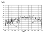
図7は、第3のポートが市販のPIM最適化された負荷によって終端されている場合であって、かつ、テストベンチによって表示可能なPIM信号の帯域幅全体が使用されるように搬送波周波数が変化する場合における、3次相互変調積の測定結果を示す。第1の実線の曲線611は、1730MHzから1785MHzまでの相互変調を示し、この場合、第1の周波数は1805MHzに固定されており、第2の周波数は1825MHzから1880MHzに変化する。第2の破線の曲線612は、1730MHzから1785MHzまでの相互変調を示し、この場合、第1の周波数は1805MHzから1832.5MHzに変化し、第2の周波数は1880MHzに固定されている。横軸は、1730から1785MHzまでの周波数を示す。縦軸は、第1の信号レベルと第2の信号レベルとの間のレベル差(+43dBmは20Wに等しい)と、相互変調信号とを、底部の−220dBcから頂部の−160dBcまでdBcで示す。明らかに、結果的に生じる−171dBcを下回る自己相互変調は、一般的なPIMテストベンチのものと変わらない。
FIG. 7 shows the case where the third port is terminated by a commercially available PIM-optimized load, and the carrier frequency is such that the entire bandwidth of the PIM signal that can be displayed by the test bench is used. The measurement result of the third-order intermodulation product in the case of changing is shown. The first
図8は、改善された負荷400を有するセットアップを示す。ここでは、テストベンチ200のDUTポート201は、改善された負荷400によって終端されている。この改善された負荷は、第2のデュプレクサ500を含み、第2のデュプレクサ500は、自身の第1のポート531を介してPIM最適化された負荷280に接続されていると共に、自身の第2のポート532を介して標準負荷に接続されている。第2のデュプレクサのTX出力部は、PIM最適化された負荷に接続されており、RX出力部は、標準負荷410によって終端されている。第2のデュプレクサは、好ましくは、第1のポート531と第3のポート533との間に接続された第1の周波数範囲のための第1のバンドパスフィルタ510を有する。第2のデュプレクサは、好ましくは、第2のポート532と第3のポート533との間に接続された第2の周波数範囲のための第2のバンドパスフィルタ520を有する。第3のポート533は、改善された負荷の入力部401として機能する。第2のデュプレクサ500の目的は、PIM最適化された負荷280によって生成されたPIM信号をブロックして、このPIM信号がPIMアナライザのテストポートに進行することができないようにすることである。DUTポート201と、改善された負荷400の入力部401との間に、被試験デバイスを接続することができる。
FIG. 8 shows a setup with an
図9は、先行する図面に示されているように、第2のデュプレクサ500によって終端された第3のポートによる測定結果を示す。この線図は、図6と比較可能である。曲線621は、曲線611と同じ条件の下での測定値を示す。曲線622は、曲線612と同じ条件の下での測定値を示す。帯域幅全体にわたって測定された相互変調は、−188dBcを下回っており、この−188dBcという値は、最も良好な市販のPIMテスタに比べてほぼ20dB優れている。
FIG. 9 shows the measurement results with the third port terminated by the
図10および図11は、検証テストの結果を示す。上記の結果は、終端部として使用されるテストベンチおよびデュプレクサのそれぞれの相互変調を減算した結果である可能性がありうる。したがって、両方の残留する相互変調積の分離を達成するために、テストベンチの第3のポートと、改善された負荷の終端するデュプレクサとの間に、工場取り付け(factory-fit)の1/2インチ超柔軟ケーブルが使用されるような検証実験が実施されてきた。伝送線路によって分離された2つのPIMソースは、信号が合計されるときに最大値を有し、信号が相殺されるときに最小値を有する、周波数にわたる周期的な相互変調レベルを結果的にもたらす。伝送線路は、観察される帯域の上側エッジと下側エッジとの間に少なくとも位相シフトの差を生じさせるような長さを有するべきである。その場合、1つの最小値および1つの最大値の周期全体が表示される。したがって、ケーブルの長さは、次のようになる:
I=vph/2Δf
vphは、位相速度であり、Δfは、テストベンチによって表示可能な相互変調積の帯域幅である。本発明の場合には、ジャンパーケーブルの位相速度は、光速の77%であり、3次相互変調積のための表示可能な周波数範囲は、第2の周波数範囲内の1730MHzから1785MHzまでである。したがって、超柔軟な1/2インチケーブルの長さは、2.1mでなければならない。
10 and 11 show the results of the verification test. The above results may be the result of subtracting the intermodulation of each of the test bench and duplexer used as the termination. Thus, to achieve isolation of both remaining intermodulation products, one-half of the factory-fit between the third port of the test bench and the duplexer terminating the improved load. Verification experiments have been conducted where an inch ultra-flexible cable is used. Two PIM sources separated by a transmission line result in a periodic intermodulation level over frequency, having a maximum when the signals are summed and a minimum when the signals are canceled . The transmission line should have a length that causes at least a phase shift difference between the upper and lower edges of the observed band. In that case, the entire cycle of one minimum and one maximum is displayed. Thus, the length of the cable is:
I = v ph / 2Δf
v ph is the phase velocity and Δf is the bandwidth of the intermodulation product that can be displayed by the test bench. In the case of the present invention, the phase velocity of the jumper cable is 77% of the speed of light, and the displayable frequency range for the third order intermodulation product is from 1730 MHz to 1785 MHz in the second frequency range. Therefore, the length of the super flexible 1/2 inch cable should be 2.1 m.
2つの異なるケーブルサンプルに関して、テスト結果が示されている。図10は、デュプレクサの第3のポートと、改善された負荷との間において第1のケーブルを使用した場合における、図9と同じ測定の結果を示す。曲線631は曲線621に対応し、曲線632は曲線622に対応する。
Test results are shown for two different cable samples. FIG. 10 shows the result of the same measurement as in FIG. 9 when using the first cable between the third port of the duplexer and the improved load.
図11は、デュプレクサの第3のポートと、改善された負荷との間において同じ長さを有する別のケーブル、すなわち、第2のケーブルを使用した場合における、図10と同じ測定の結果を示す。曲線641は曲線631に対応し、曲線642は曲線632に対応する。
FIG. 11 shows the result of the same measurement as in FIG. 10 when using another cable having the same length between the third port of the duplexer and the improved load, ie the second cable .
両方の測定に関してPIMレベルは、約1765MHzにおいて最大値を有し、約1732MHzにおいて最小値を有する。この結果は、2.75m(=2.1m/77%)の電気的距離を有する2つのソースの信号が合計されたときの、相互変調積の周波数依存性の挙動に対する期待を満たすものである。最大値は、両方の信号の合計を示すので、テストベンチの残留PIMは、測定帯域全体にわたって+43dBmの搬送波電力において−185dBcより良好であると結論付けることができる。 The PIM level for both measurements has a maximum at about 1765 MHz and a minimum at about 1732 MHz. This result fulfills the expectation for the frequency dependent behavior of intermodulation products when the signals of two sources with an electrical distance of 2.75 m (= 2.1 m / 77%) are summed . Since the maximum value indicates the sum of both signals, it can be concluded that the residual PIM of the test bench is better than -185 dBc at +43 dBm carrier power throughout the measurement band.
この検証には依然として弱点があることに言及しなければならない。すなわち、同軸ケーブルのPIMが無視できるほどわずかであることが仮定されているのである。しかしながら、ケーブルおよびコネクタは線状材料から形成されており、また、ケーブルの内部導体と外部導体との間の接合部と工場取り付けのコネクタとははんだ付けされており、このことは、非常に小さい相互変調積につながるはずである。さらに、テストの実施により、多数のケーブルサンプルに関して同様の結果が得られている。したがって、測定値が、ケーブルの自己相互変調の代わりに、テストベンチの残留PIM示す可能性が非常に高い。 It should be mentioned that this verification still has weaknesses. That is, it is assumed that the PIM of the coaxial cable is negligible. However, the cables and connectors are formed from linear material, and the joints between the inner and outer conductors of the cables and the factory-installed connectors are soldered, which is very small It should lead to intermodulation products. In addition, test runs have yielded similar results for a large number of cable samples. Thus, it is very likely that the measurement will show the residual PIM of the test bench instead of the cable self-intermodulation.
100 デュプレクサ
110 第1のデュプレクサフィルタ
120 第2のデュプレクサフィルタ
131 第1のポート
132 第2のポート
133 第3のポート
151 第1のポートから第3のポートへの挿入損失
152 第3のポートから第2のポートへの挿入損失
161 第1の周波数範囲
162 第2の周波数範囲
200 PIMテストベンチ
201 テストベンチのDUTポート
210 第1の信号発生器
211 第1の電力増幅器
212 第1のサーキュレータ
213 第1のサーキュレータ終端部
218 第1の周波数
220 第2の信号発生器
221 第2の電力増幅器
222 第2のサーキュレータ
223 第2のサーキュレータ終端部
228 第2の周波数
230 方向性カプラ
231 方向性カプラ終端部
240 第1のアイソレーションフィルタ
250 第2のアイソレーションフィルタ
260 LNA(low noise amplifier:低雑音増幅器)
270 スペクトルアナライザ
280 PIM最適化された負荷
300 DUT(device under test:被試験デバイス)
400 改善された負荷
401 改善された負荷の入力部
410 標準負荷
500 第2のデュプレクサ
510 第1のデュプレクサフィルタ
520 第2のデュプレクサフィルタ
531 第1のポート
532 第2のポート
533 第3のポート
611 PIM最適化された負荷による第1の相互変調曲線
612 PIM最適化された負荷による第2の相互変調曲線
621 改善された負荷による第1の相互変調曲線
622 改善された負荷による第2の相互変調曲線
631 改善された負荷および第1のケーブルによる第1の相互変調曲線
632 改善された負荷および第1のケーブルによる第2の相互変調曲線
641 改善された負荷および第2のケーブルによる第1の相互変調曲線
642 改善された負荷および第2のケーブルによる第2の相互変調曲線
700 デュプレクサのハウジング本体
710 カバー結合面
711 絶縁されたねじのための孔
715 シールド接触面
719 中空空間
720 接触ストリップ
740 共振器ロッド
741 同調要素
731 第1のポートコネクタ
732 第2のポートコネクタ
733 第3のポートコネクタ
736 第1のポートの容量性カプラ
737 第2のポートの容量性カプラ
738 第3のポートの容量性カプラ
740 同軸共振器ロッド
741 誘電性の同調要素
742 共振器間カップリング
745 同調要素のための固定ナット
750 容量性カップリング
760 ガルバニック接触
780 金属製のカバー
781 本体結合面
782 絶縁されたねじ
790 シールド
795 本体接触面
DESCRIPTION OF
270
400
Claims (14)
前記ハウジングは、モノリシックな金属製の本体(700)を含み、前記フィルタは、少なくとも1つの同軸共振器ロッド(740)を含む、
フィルタにおいて、
前記ハウジングは、如何なるガルバニック接触をも有することなく前記本体に容量的に結合された金属製のカバー(780)を含む、
ことを特徴とするフィルタ。 A filter for an RF signal, comprising at least one filter component (740, 742) and a metal housing,
The housing comprises a monolithic metallic body (700) and the filter comprises at least one coaxial resonator rod (740)
In the filter
The housing includes a metallic cover (780) capacitively coupled to the body without any galvanic contact.
A filter characterized by
請求項1記載のフィルタ。 At least one of the coaxial resonator rods (740) is at least a portion of a housing body (700),
The filter of claim 1.
請求項1または2記載のフィルタ。 The cover (780) has a dielectric layer at least on the side facing the housing body (700) or on the whole side of the cover (780),
The filter according to claim 1 or 2.
請求項1から3までのいずれか1項記載のフィルタ。 The body (700) has a dielectric layer at least on the side facing the housing cover (780) or on the whole side of the body (700),
A filter according to any one of the preceding claims.
請求項1から4までのいずれか1項記載のフィルタ。 The body has a cover coupling surface (710) that coincides with the body coupling surface (781) of the cover,
5. A filter according to any one of the preceding claims.
請求項5記載のフィルタ。 At least one of the cover bonding surface and the body bonding surface has a dielectric layer,
The filter according to claim 5 .
請求項3、4および6のいずれか1項記載のフィルタ。 The dielectric layer comprises at least one of a coating, an oxide layer, an anodized layer, an oxide, an optional ceramic material, a paint, a plastic film, a polymer material, or any combination thereof.
A filter according to any one of claims 3, 4 and 6.
請求項1から7までのいずれか1項記載のフィルタ。 The cover is fixed to the housing body by means of an insulating material, preferably by means of screws, bolts or pins made of glass fiber reinforced plastic.
A filter according to any one of the preceding claims.
前記シールド(790)は、好ましくは少なくとも1つの本体接触面(795)を有し、前記本体接触面(795)を介して前記シールドの少なくとも1つのシールド接触面(715)とガルバニック接触している、
請求項1から8までのいずれか1項記載のフィルタ。 A shield (790) is provided to cover the cover (780),
The shield (790) preferably has at least one body contact surface (795) and is in galvanic contact with at least one shield contact surface (715) of the shield via the body contact surface (795) ,
9. A filter according to any one of the preceding claims.
前記デュプレクサは、第1のバンドパスフィルタを介して第3のポートに接続された第1のポートと、第2のバンドパスフィルタを介して前記第3のポートに接続された第2のポートとを有する、
請求項1から9までのいずれか1項記載のフィルタ。 The filter is a duplexer,
The duplexer includes a first port connected to a third port via a first band pass filter, and a second port connected to the third port via a second band pass filter. Have
10. A filter according to any one of the preceding claims.
請求項1から10までのいずれか1項記載のフィルタ。 The filter is a duplexer comprising six elliptical cavity filter components,
11. A filter according to any one of the preceding claims.
・前記フィルタの少なくとも1つのポートカプラは、容量性である、
・前記フィルタの少なくとも1つのポートカプラは、コネクタのモノリシックな内部導体の一部である、
・共振器のための少なくとも1つの同調要素が設けられており、好ましくは酸化アルミニウムを含む、
・少なくとも1つの共振器間カップリングは、アルミニウムから形成されており、誘電体層を有する、
・前記同調要素を固定するためのナットは、前記同調要素および前記カバーのいずれにもガルバニック接触しないように絶縁されている、
・前記フィルタの全ての要素は、モノリシックな部品であり、前記要素間の接合部は、ガルバニック接触を回避するために誘電性のコーティングを間に有する、
・複数のモノリシックな要素の間の全ての静電容量は、線形性への悪影響を有することなく、所望の周波数範囲内でのガルバニック接触に代わる適切な置換えとなるために十分に低いインピーダンスを提供するように、ガルバニック接触を有することなく容量性カップリングを提供するように設計されている、
のうちの少なくとも1つを含む、
請求項1から11までのいずれか1項記載のフィルタ。 The following features:
The at least one port coupler of the filter is capacitive,
The at least one port coupler of the filter is part of a monolithic inner conductor of the connector,
At least one tuning element for the resonator is provided, preferably comprising aluminum oxide
At least one inter-resonator coupling is made of aluminum and has a dielectric layer,
A nut for securing the tuning element is insulated so as not to have galvanic contact with either of the tuning element and the cover,
All elements of the filter are monolithic parts and the joints between the elements have dielectric coatings in between to avoid galvanic contact,
-All capacitances between multiple monolithic elements provide sufficiently low impedance to be a suitable replacement for galvanic contact in the desired frequency range without having an adverse effect on linearity Are designed to provide capacitive coupling without having galvanic contact ,
Containing at least one of
12. A filter according to any one of the preceding claims.
請求項1から12までのいずれか1項記載のフィルタを少なくとも1つ含み、前記フィルタは、第1のバンドパスフィルタを介して第3のポートに接続された第1のポートと、第2のバンドパスフィルタを介して前記第3のポートに接続された第2のポートとを有する第1のデュプレクサであり、
前記PIMテストベンチは、
前記第1のポートに接続された、第1の周波数および第2の周波数でRF信号を供給する少なくとも1つのRF信号源と、
前記第2のポートに接続されたスペクトルアナライザと、
前記第3のポートに接続された負荷と、
を含み、前記第3のポートと前記負荷との間にDUTを接続するための手段が設けられている、
テストベンチ。 A test bench for measuring passive intermodulation or PIM,
A filter comprising at least one filter according to any one of claims 1 to 12, wherein the filter comprises: a first port connected to a third port via a first band pass filter; A first duplexer having a second port connected to the third port via a band pass filter,
The PIM test bench is
At least one RF signal source connected to the first port for supplying an RF signal at a first frequency and a second frequency;
A spectrum analyzer connected to the second port;
A load connected to the third port;
Means are provided for connecting a DUT between the third port and the load,
Test bench.
前記第2のデュプレクサは、
当該第2のデュプレクサの第3のポートによって前記第1のデュプレクサの第3のポートに接続されており、
当該第2のデュプレクサの第1のポートまたは第2のポートによって前記負荷に接続されており、
当該第2のデュプレクサの第2のポートまたは第1のポートによって前記標準負荷に接続されており、
前記第1のデュプレクサの前記第3のポートと前記第2のデュプレクサの前記第3のポートとの間にDUTを接続するための手段が設けられている、
請求項13記載のテストベンチ。 Including a second duplexer and a standard load,
The second duplexer is
Connected to a third port of the first duplexer by a third port of the second duplexer,
Connected to the load by a first port or a second port of the second duplexer,
Connected to the standard load by a second port or a first port of the second duplexer,
Means are provided for connecting a DUT between the third port of the first duplexer and the third port of the second duplexer.
The test bench of claim 13.
Applications Claiming Priority (3)
| Application Number | Priority Date | Filing Date | Title |
|---|---|---|---|
| EP16154517.3 | 2016-02-05 | ||
| EP16154517 | 2016-02-05 | ||
| PCT/EP2017/052429 WO2017134246A1 (en) | 2016-02-05 | 2017-02-03 | Filter structures for pim measurements |
Publications (2)
| Publication Number | Publication Date |
|---|---|
| JP6526345B1 true JP6526345B1 (en) | 2019-06-05 |
| JP2019517165A JP2019517165A (en) | 2019-06-20 |
Family
ID=55315340
Family Applications (1)
| Application Number | Title | Priority Date | Filing Date |
|---|---|---|---|
| JP2018540762A Active JP6526345B1 (en) | 2016-02-05 | 2017-02-03 | Filter structure for PIM measurement |
Country Status (7)
| Country | Link |
|---|---|
| US (1) | US10403949B2 (en) |
| EP (1) | EP3203575B1 (en) |
| JP (1) | JP6526345B1 (en) |
| KR (1) | KR101980791B1 (en) |
| CN (1) | CN108886190B (en) |
| ES (1) | ES2713707T3 (en) |
| WO (1) | WO2017134246A1 (en) |
Families Citing this family (10)
| Publication number | Priority date | Publication date | Assignee | Title |
|---|---|---|---|---|
| US10512120B2 (en) * | 2017-04-11 | 2019-12-17 | Wilson Electronics, Llc | Signal booster with coaxial cable connections |
| CN111226402B (en) * | 2017-06-27 | 2022-08-19 | 凯镭思有限公司 | System and apparatus for identifying faults in a radio frequency device or system |
| WO2019143869A1 (en) | 2018-01-17 | 2019-07-25 | Ppc Broadband, Inc. | Modular rf devices |
| CN110470970B (en) * | 2019-07-09 | 2021-09-21 | 广州兴森快捷电路科技有限公司 | Method for dynamically monitoring passive intermodulation |
| CN110943790A (en) * | 2019-12-15 | 2020-03-31 | 南京纳特通信电子有限公司 | Blind plugging table type intermodulation tester |
| CN113036342A (en) * | 2019-12-25 | 2021-06-25 | 深圳市大富科技股份有限公司 | Communication system and filter thereof |
| CN113036354A (en) * | 2019-12-25 | 2021-06-25 | 深圳市大富科技股份有限公司 | Filter and communication equipment |
| CN111799534B (en) | 2020-06-08 | 2021-06-01 | 南京邮电大学 | Four-order Ka-band-pass filter based on printed ridge gap waveguide |
| CN112564833B (en) * | 2020-11-24 | 2022-02-22 | 电子科技大学 | Novel passive intermodulation test system and method for W-band waveguide structure |
| KR102437243B1 (en) * | 2021-05-27 | 2022-09-02 | 주식회사 이지스 | Wireless communication apparatus capable of improving PIMD |
Family Cites Families (21)
| Publication number | Priority date | Publication date | Assignee | Title |
|---|---|---|---|---|
| US4307357A (en) | 1980-03-04 | 1981-12-22 | Tektronix, Inc. | Foreshortened coaxial resonators |
| JPS63308401A (en) | 1987-06-09 | 1988-12-15 | Nec Corp | Coaxial branching filter |
| GB9114970D0 (en) * | 1991-07-11 | 1991-08-28 | Filtronics Components | Microwave filter |
| US5329687A (en) * | 1992-10-30 | 1994-07-19 | Teledyne Industries, Inc. | Method of forming a filter with integrally formed resonators |
| US6366183B1 (en) | 1999-12-09 | 2002-04-02 | Hughes Electronics Corp. | Low PIM coaxial diplexer interface |
| US20060135092A1 (en) * | 2004-12-16 | 2006-06-22 | Kathrein Austria Ges. M. B. H. | Radio frequency filter |
| WO2008029522A1 (en) | 2006-09-06 | 2008-03-13 | Yokohama National University | Passive intermodulation distortion measuring method and system |
| EP2092593B1 (en) | 2006-11-13 | 2012-11-28 | KMW Inc. | Radio frequency filter |
| CN101627503A (en) * | 2006-11-13 | 2010-01-13 | Kmw株式会社 | Radio frequency filter |
| EP2099091B1 (en) * | 2008-03-04 | 2017-11-22 | HMD global Oy | Variable radio frequency band filter |
| KR101569730B1 (en) | 2009-03-18 | 2015-11-18 | 주식회사 에이스테크놀로지 | Tuning Bolt Ground Connection Structure and RF Caivity Filter Having the Same |
| US9306261B2 (en) | 2009-06-04 | 2016-04-05 | Purdue Research Foundation | Magnetic field system and method for mitigating passive intermodulation distortion |
| US8742869B2 (en) | 2010-03-16 | 2014-06-03 | K&L Microwave, Inc. | Low passive inter-modulation capacitor |
| KR101187362B1 (en) * | 2010-12-20 | 2012-10-02 | 한국항공우주연구원 | Corona Free Diplexer for Launcher Space Applications |
| FR2977381B1 (en) * | 2011-06-30 | 2014-06-06 | Alcatel Lucent | DEHASTER AND POWER DISTRIBUTOR |
| FI125953B (en) * | 2011-10-18 | 2016-04-29 | Tongyo Technology Oy | Method of manufacturing an RF filter and an RF filter |
| DE102014011514A1 (en) * | 2014-07-31 | 2016-02-04 | Kathrein-Werke Kg | Capacitor-lubricated housing, in particular capacitively lubricated component housing for an antenna device |
| EP3048672A1 (en) * | 2015-01-22 | 2016-07-27 | Spinner GmbH | Low passive intermodulation coaxial connector test interface |
| US9647306B2 (en) * | 2015-03-04 | 2017-05-09 | Skyworks Solutions, Inc. | RF filter comprising N coaxial resonators arranged in a specified interdigitation pattern |
| PL3217469T3 (en) * | 2016-03-11 | 2019-01-31 | Nokia Solutions And Networks Oy | Radio-frequency filter |
| KR102343774B1 (en) * | 2017-03-22 | 2021-12-28 | 주식회사 에이스테크놀로지 | Rf filter for improving pimd performance |
-
2017
- 2017-02-03 ES ES17154615T patent/ES2713707T3/en active Active
- 2017-02-03 EP EP17154615.3A patent/EP3203575B1/en active Active
- 2017-02-03 WO PCT/EP2017/052429 patent/WO2017134246A1/en active Application Filing
- 2017-02-03 KR KR1020187025636A patent/KR101980791B1/en active IP Right Grant
- 2017-02-03 CN CN201780009447.7A patent/CN108886190B/en active Active
- 2017-02-03 JP JP2018540762A patent/JP6526345B1/en active Active
-
2018
- 2018-08-02 US US16/053,303 patent/US10403949B2/en active Active
Also Published As
| Publication number | Publication date |
|---|---|
| KR20180125958A (en) | 2018-11-26 |
| US20180342779A1 (en) | 2018-11-29 |
| US10403949B2 (en) | 2019-09-03 |
| CN108886190A (en) | 2018-11-23 |
| CN108886190B (en) | 2019-11-05 |
| EP3203575B1 (en) | 2018-12-05 |
| ES2713707T3 (en) | 2019-05-23 |
| KR101980791B1 (en) | 2019-05-21 |
| WO2017134246A1 (en) | 2017-08-10 |
| JP2019517165A (en) | 2019-06-20 |
| EP3203575A1 (en) | 2017-08-09 |
Similar Documents
| Publication | Publication Date | Title |
|---|---|---|
| JP6526345B1 (en) | Filter structure for PIM measurement | |
| Parment et al. | Low-loss air-filled substrate integrated waveguide (SIW) band-pass filter with inductive posts | |
| CN110739512B (en) | Balanced filtering cross junction with high common-mode rejection | |
| US20170352937A1 (en) | Method to design and assemble a connector for the transition between a coaxial cable and a microstrip line | |
| WO2019064510A1 (en) | High frequency filter | |
| US8742869B2 (en) | Low passive inter-modulation capacitor | |
| JP2000040901A (en) | Dielectric filter, dielectric duplexer and communication machine equipment | |
| US10056663B2 (en) | Intermodulation distortion reduction system using insulated tuning elements | |
| Vallerotonda et al. | Dielectric-loaded L-band filters for high-power space applications | |
| Aryanfar et al. | Compact millimeter-wave filters using distributed capacitively loaded CPW resonators | |
| US11742557B2 (en) | Dielectric waveguide filter | |
| JP3580529B2 (en) | Coaxial circulator and duplexer | |
| Grassl et al. | Novel design features for the improvement of linearity in filter structures for PIM measurements | |
| Li et al. | A Ka-band transceiver module based on LTCC technology | |
| CN111033884B (en) | Filter, duplexer and communication equipment | |
| Moscato et al. | Ku/Ka band diplexer based on thin-film technology for small ground-segment user terminals | |
| JP2007150750A (en) | Dielectric resonator and dielectric filter | |
| Konpang et al. | Four‐port diplexer for high Tx/Rx isolation for integrated transceivers | |
| EP3104451A1 (en) | Resonator assembly and filter | |
| Heinikoski et al. | Wideband Complex Permittivity Tester for 5G Materials | |
| Wang et al. | Compact substrate integrated waveguide bandstop filter based on CSRRs | |
| Lucicanin et al. | Higher order mode suppression in triaxial cells | |
| KR100683007B1 (en) | Coaxial to waveguide transition apparatus for embodying airline coaxial line | |
| Zhang et al. | A Compact Differential-Mode Wide Stopband Bandpass Filter with Good and Wideband Common-Mode Suppression | |
| Ibrahim et al. | A new RF interference cancellation using a novel 3-pole bandstop resonator designed using tapped CRLH T-line model |
Legal Events
| Date | Code | Title | Description |
|---|---|---|---|
| A521 | Request for written amendment filed |
Free format text: JAPANESE INTERMEDIATE CODE: A523 Effective date: 20180903 Free format text: JAPANESE INTERMEDIATE CODE: A523 Effective date: 20180928 |
|
| A621 | Written request for application examination |
Free format text: JAPANESE INTERMEDIATE CODE: A621 Effective date: 20180903 |
|
| A871 | Explanation of circumstances concerning accelerated examination |
Free format text: JAPANESE INTERMEDIATE CODE: A871 Effective date: 20180903 |
|
| A975 | Report on accelerated examination |
Free format text: JAPANESE INTERMEDIATE CODE: A971005 Effective date: 20181205 |
|
| A131 | Notification of reasons for refusal |
Free format text: JAPANESE INTERMEDIATE CODE: A131 Effective date: 20181218 |
|
| A521 | Request for written amendment filed |
Free format text: JAPANESE INTERMEDIATE CODE: A523 Effective date: 20190314 |
|
| TRDD | Decision of grant or rejection written | ||
| A01 | Written decision to grant a patent or to grant a registration (utility model) |
Free format text: JAPANESE INTERMEDIATE CODE: A01 Effective date: 20190401 |
|
| A61 | First payment of annual fees (during grant procedure) |
Free format text: JAPANESE INTERMEDIATE CODE: A61 Effective date: 20190507 |
|
| R150 | Certificate of patent or registration of utility model |
Ref document number: 6526345 Country of ref document: JP Free format text: JAPANESE INTERMEDIATE CODE: R150 |
|
| R250 | Receipt of annual fees |
Free format text: JAPANESE INTERMEDIATE CODE: R250 |
|
| R250 | Receipt of annual fees |
Free format text: JAPANESE INTERMEDIATE CODE: R250 |