JP6524944B2 - Vapor phase etching method and epitaxial substrate manufacturing method - Google Patents
Vapor phase etching method and epitaxial substrate manufacturing method Download PDFInfo
- Publication number
- JP6524944B2 JP6524944B2 JP2016055179A JP2016055179A JP6524944B2 JP 6524944 B2 JP6524944 B2 JP 6524944B2 JP 2016055179 A JP2016055179 A JP 2016055179A JP 2016055179 A JP2016055179 A JP 2016055179A JP 6524944 B2 JP6524944 B2 JP 6524944B2
- Authority
- JP
- Japan
- Prior art keywords
- temperature
- vapor phase
- susceptor
- chamber
- phase etching
- Prior art date
- Legal status (The legal status is an assumption and is not a legal conclusion. Google has not performed a legal analysis and makes no representation as to the accuracy of the status listed.)
- Active
Links
Images

Description
本発明は、気相成長装置において実施される気相エッチング方法に関し、より詳しくは、気相成長装置のチャンバー内のウォールデポを除去するための気相エッチング方法及びそれを用いたエピタキシャル基板の製造方法に関する。 The present invention relates to a vapor phase etching method implemented in a vapor phase growth apparatus, and more particularly, to a vapor phase etching method for removing a wall deposit in a chamber of the vapor phase growth apparatus and manufacture of an epitaxial substrate using the same. On the way.
半導体基板(以下基板という)であるシリコンウェーハを用いて、コンピュータのメモリや演算素子、またデジタルカメラやビデオの撮像素子等、さまざまなデバイスが作られている。特に、先端向けのデバイスには、シリコンウェーハの表面に気相成長によりシリコン層を堆積させたエピタキシャルシリコンウェーハ(エピウェーハ)が用いられている。 A variety of devices such as computer memories and computing elements, digital cameras, video imaging elements, and the like are manufactured using a silicon wafer which is a semiconductor substrate (hereinafter referred to as a substrate). In particular, an epitaxial silicon wafer (epi wafer) in which a silicon layer is deposited by vapor deposition on the surface of a silicon wafer is used for a device for leading edge.
一般的にエピウェーハは、1100℃以上の高温でトリクロロシラン等の原料を気相反応させ、シリコン基板上にエピタキシャルシリコン層を成膜させ作られる。気相成長装置では、ウェーハと前記ウェーハを載置するサセプタをヒーターで加熱し、炉体を冷却するコールドウォール式の装置が一般的である。 In general, an epi-wafer is produced by vapor phase reaction of a raw material such as trichlorosilane at a high temperature of 1100 ° C. or higher to form an epitaxial silicon layer on a silicon substrate. In a vapor phase growth apparatus, a cold wall type apparatus is generally used which heats a wafer and a susceptor on which the wafer is placed with a heater and cools a furnace body.
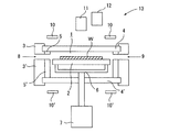
図4に、気相成長装置の透明石英部材で封止されたチャンバーの様子を模式的に示す。
気相成長装置は、サセプタ支持具6に支持されてウェーハWを載置するサセプタ2を具備するチャンバー1を有している。チャンバー1は、上下に設置された透明石英部材4,4’によって封止される構成となっている。透明石英部材4,4’を通してウェーハWおよびサセプタ2を昇温するため、チャンバー上部および下部にランプ等のヒーター10が設置される。
FIG. 4 schematically shows the state of the chamber sealed with the transparent quartz member of the vapor phase growth apparatus.
The vapor phase growth apparatus has a
エピタキシャル成長反応はシリコン基板であるウェーハW上で発生すると同時に、サセプタ2上やチャンバー1の壁面上でも反応し、ポリシリコンや珪素化合物が副生成物として堆積する。このような副生成物はウォールデポ(ウォールデポジション)と呼ばれる。図4に示すように、ウォールデポ14がウェーハWと加熱用ランプであるヒーター10の間の透明石英部材4上に付着すると、エピタキシャル反応中に壁面から剥離し、前記ウェーハW上に付着することでパーティクルとなる。
The epitaxial growth reaction occurs on the wafer W, which is a silicon substrate, and also reacts on the
また、ウォールデポ14が生成されると、図4に示すようにヒーター10の照射光15を遮ることとなってしまい、ウォールデポ14によって影となる領域の温度が低下し、温度分布が悪化するため、エピタキシャルウェーハの膜厚分布・抵抗分布が悪化し、スリップ転位が発生しやすくなる。
Further, when the
さらに、気相成長装置の透明石英部材で封止されたチャンバー1において、前記透明石英部材4,4’上に生成するウォールデポ14は、シリコン基板の温度を測定するパイロメーターに入射する輻射光を遮り、測定温度の精度を悪化させる。
Furthermore, in the
故に、ウォールデポは定期的に除去する必要があり、ウォールデポの除去には塩化水素ガス(HCl)を用いた気相エッチングが行われる。しかし、過度にエッチングを行うと、チャンバーの部材の寿命を低下させるとともに、サイクルタイムが増加し、生産性が悪化するという問題があった。 Therefore, the wall deposits need to be removed regularly, and the removal of the wall deposits is carried out by vapor phase etching using hydrogen chloride gas (HCl). However, excessive etching reduces the life of the chamber members, increases the cycle time, and deteriorates the productivity.
前述のように、気相成長においてはHClを用いた気相エッチングにより定期的にウォールデポを除去する必要がある。必要なエッチングの時間は、反応したエピタキシャル膜の厚さの累積に応じて変化する。種々のエピタキシャル膜厚・エッチング時間でチャンバー内のウォールデポ残存量を評価し、必要なエッチング時間を計算する。 As described above, in vapor deposition, it is necessary to remove the wall deposit periodically by vapor etching using HCl. The required etching time varies as the thickness of the reacted epitaxial film is accumulated. Evaluate the amount of wall deposit remaining in the chamber with various epitaxial film thickness and etching time, and calculate the required etching time.
しかしながら、上記ウォールデポ残存量の評価は目視で行うため、必ずしも正確ではない。また、必要なエッチング時間は、反応したエピタキシャル膜厚の累積だけでなく、ソースガス種やプロセス温度、キャリアガス流量等のエピタキシャル反応条件にも影響を受ける。 However, the evaluation of the remaining amount of the wall deposit is not always accurate because it is performed visually. Further, the required etching time is influenced not only by the accumulation of the reacted epitaxial film thickness but also by the epitaxial reaction conditions such as the source gas species, the process temperature and the carrier gas flow rate.
このように、エッチング時間はエピタキシャル膜厚の累計に加え、確実にエッチングを行うためには、オーバーエッチング時間の導入が必要となる。しかし、過度のエッチングはSiC部材からなるサセプタにダメージを与えてしまう。また、エッチング時間の増大は生産性を悪化させてしまう。 As described above, the etching time is added to the total of the epitaxial film thickness, and in order to perform the etching reliably, the introduction of the over etching time is required. However, excessive etching damages the susceptor made of a SiC member. In addition, an increase in etching time deteriorates productivity.
本発明は上記従来技術の問題点に鑑みなされたもので、気相成長装置のチャンバー内に堆積したウォールデポをエッチングにより除去する際、エッチング時間を短縮でき、オーバーエッチングによるサセプタのダメージを減少させ、生産性を向上することができる気相エッチング方法及びエピタキシャル基板の製造方法を提供することを目的とする。 The present invention has been made in view of the above-mentioned problems of the prior art, and when removing the wall deposit deposited in the chamber of the vapor phase growth apparatus by etching, the etching time can be shortened and damage to the susceptor due to overetching can be reduced. It is an object of the present invention to provide a vapor phase etching method and an epitaxial substrate manufacturing method capable of improving the productivity.
上記課題を解決するため、本発明の気相エッチング方法は、基板が載置されるサセプタと、前記サセプタが収容され、透明石英部材により封止されたチャンバーと、前記チャンバーの外側に設けられ、測定光路が前記透明石英部材の内壁面上のウォールデポの生成が予測される箇所を横切って前記チャンバー内のサセプタ温度を測定するように設置されたサセプタ温度測定用パイロメーターと、を有する気相成長装置において実施される気相エッチング方法であり、前記チャンバー内を昇温させ、前記ウォールデポの存在しない状態での前記サセプタ温度を予め測定することにより基準温度を設定しておく工程と、前記チャンバー内を昇温させた状態での前記サセプタ温度が前記基準温度よりも低い場合には、前記ウォールデポが生成されているものとみなして気相エッチングを行う気相エッチング開始工程と、前記サセプタ温度が前記基準温度となったら前記気相エッチングを終了する気相エッチング終了工程と、を含む気相エッチング方法、である。 In order to solve the above problems, the vapor phase etching method of the present invention is provided on a susceptor on which a substrate is placed, a chamber containing the susceptor, sealed by a transparent quartz member, and outside the chamber. A susceptor temperature measuring pyrometer installed to measure a susceptor temperature in the chamber across a location where a measurement light path is expected to generate a wall deposit on the inner wall surface of the transparent quartz member A vapor phase etching method implemented in a growth apparatus, wherein the temperature in the chamber is raised, and a reference temperature is set by measuring in advance the susceptor temperature in the absence of the wall deposit; When the temperature of the susceptor with the temperature in the chamber raised is lower than the reference temperature, the wall deposit is generated. A vapor phase etching start step of performing vapor phase etching on the assumption that the gas phase etching is performed, and a vapor phase etching end step of terminating the vapor phase etching when the susceptor temperature reaches the reference temperature. .
コールドウォール型の気相成長装置は、サセプタをヒーターで加熱し、炉体を冷却しながらエピタキシャル反応および気相エッチングを行う。気相エッチングは高温であると反応効率が高いため、サセプタ上のウォールデポは除去が容易であるのに対し、チャンバー壁面のウォールデポは長時間のエッチングが必要となる。特に透明石英部材は昇温しづらく、前記透明石英部材上のウォールデポはエッチング残りとなりやすい。 The cold wall type vapor phase growth apparatus heats the susceptor with a heater, and performs epitaxial reaction and vapor phase etching while cooling the furnace body. Since the reaction efficiency is high at a high temperature in the vapor phase etching, the wall deposits on the susceptor are easy to remove, whereas the wall deposits on the chamber wall surfaces need to be etched for a long time. In particular, the temperature of the transparent quartz member is hard to increase, and the wall deposit on the transparent quartz member tends to be unetched.
このため、前記チャンバー内の透明石英部材上のウォールデポが除去されたタイミングでは、前記チャンバー内の透明石英部材上以外の箇所に堆積しているウォールデポについても既に除去されたとみなすことができる。故に、気相エッチング中におけるチャンバー内の透明石英部材上のウォールデポを逐次検出し、前記ウォールデポが除去されたタイミングで気相エッチングを終了するようにすれば、エッチング時間を最小限に抑え、サセプタのダメージを減少させ、生産性を向上することができる。 For this reason, at the timing when the wall deposit on the transparent quartz member in the chamber is removed, it can be considered that the wall deposit deposited on a place other than on the transparent quartz member in the chamber has already been removed. Therefore, if the wall deposits on the transparent quartz member in the chamber are sequentially detected during the gas phase etching, and the gas phase etching is finished at the timing when the wall deposits are removed, the etching time is minimized. The damage to the susceptor can be reduced and the productivity can be improved.
前記チャンバー内の透明石英部材上のウォールデポ検出方法として、サセプタ温度測定用にパイロメーター(放射温度計)を使用する。サセプタ温度測定用パイロメーターは、チャンバー外部から透明石英部材を通してサセプタ表面の温度を測定し、かつ、前記チャンバー内の透明石英部材上のウォールデポの生成が予測される箇所が、前記サセプタ表面の温度測定点と前記サセプタ温度測定用パイロメーターの検出部との間の測定光路を横切る位置に設置する。 As a method for detecting a wall deposit on a transparent quartz member in the chamber, a pyrometer (a radiation thermometer) is used for susceptor temperature measurement. The susceptor temperature measurement pyrometer measures the temperature of the susceptor surface from the outside of the chamber through the transparent quartz member, and the place where generation of a wall deposit on the transparent quartz member in the chamber is predicted is the temperature of the susceptor surface It is installed at a position crossing the measurement light path between the measurement point and the detection unit of the susceptor temperature measurement pyrometer.
前記チャンバー内の透明石英部材上にウォールデポ生成がある場合、前記ウォールデポがサセプタ表面の輻射光を反射・吸収し、サセプタ温度測定用パイロメーターの測定値が実際の温度より低く表示される。一定のヒーター出力でサセプタを加熱しながら気相エッチングを行うと、次第に透明石英部材上のウォールデポが除去され、前記サセプタ表面温度の測定値が増加する。 When the wall deposit is generated on the transparent quartz member in the chamber, the wall deposit reflects and absorbs the radiation on the surface of the susceptor, and the measured value of the susceptor temperature measurement pyrometer is displayed lower than the actual temperature. When vapor phase etching is performed while heating the susceptor with a constant heater output, the wall deposit on the transparent quartz member is gradually removed, and the measured value of the susceptor surface temperature is increased.
ウォールデポ生成が無い状態における所定のヒーター出力でのサセプタ温度を予め測定し基準温度を設定しておき、ヒーターを前記出力に制御しながら気相エッチングを行い、サセプタが前記基準温度に到達したときにエッチングを終了するようにすれば、チャンバー内にウォールデポ除去残りがなく、かつ、エッチング時間を最小限とすることができる。 When the susceptor temperature at a predetermined heater output without wall deposition is measured in advance and a reference temperature is set, vapor phase etching is performed while controlling the heater to the output, and the susceptor reaches the reference temperature If the etching is finished, there is no residue left to remove the wall deposit in the chamber, and the etching time can be minimized.
前記チャンバーのウォールデポの生成が予測される内壁面の箇所としては、前記チャンバーの透明石英部材の内壁面上におけるウォールデポが形成されやすい箇所とすればよい。特に、前記チャンバーの透明石英部材の内壁面上の最もウォールデポが形成されやすい箇所を前記チャンバーのウォールデポの生成が予測される内壁面の箇所として、サセプタ温度測定用パイロメーターを設置するのが好適である。 The portion of the inner wall surface where generation of a wall deposit of the chamber is predicted may be a portion on the inner wall surface of the transparent quartz member of the chamber which is likely to be formed. In particular, a susceptor temperature measurement pyrometer is installed on the inner wall surface of the transparent quartz member of the chamber where the wall deposit is most likely to be formed as a portion of the inner wall surface where generation of the wall deposit of the chamber is expected. It is suitable.
前記気相エッチング終了工程において、前記サセプタ温度が所定の温度となるようにヒーター出力を制御し、前記ヒーター出力が所定の値となったときに、前記サセプタ温度が前記基準温度となったとみなして前記気相エッチングを終了するようにしてもよい。 In the vapor phase etching end step, the heater output is controlled so that the susceptor temperature becomes a predetermined temperature, and when the heater output becomes a predetermined value, it is considered that the susceptor temperature becomes the reference temperature The gas phase etching may be ended.
即ち、前述のように、ヒーター出力を一定に制御しながら気相エッチングを行い、サセプタが所定の温度となったタイミングでエッチングを終了する方法と同様に、サセプタ温度を一定に制御しながら気相エッチングを行い、ヒーター出力が所定の値となったタイミングで、前記サセプタ温度が前記基準温度となったとみなしてエッチングを終了する方法でも、エッチング時間の短縮が実現できる。 That is, as described above, the vapor phase etching is performed while controlling the heater output constant, and the vapor phase etching is controlled constant as in the method of ending the etching when the susceptor reaches a predetermined temperature. The etching time can be shortened also by a method in which etching is performed and the etching is finished by regarding the susceptor temperature as the reference temperature at the timing when the heater output reaches a predetermined value.
透明石英部材上にウォールデポの堆積がある場合、サセプタ温度測定用パイロメーターによるサセプタ温度の測定値が低下する。サセプタ温度が一定となるようにヒーター出力をフィードバック制御すると、気相エッチングにより次第にヒーター出力が低下する。ウォールデポが無い場合における、サセプタ温度を所定の値に制御したときのヒーター出力を予め測定しておき、サセプタ温度を一定に制御しながら気相エッチングを行い、サセプタが前記ヒーター出力に到達したときにエッチングを終了することで、チャンバー内にウォールデポ除去残りなく、かつ、エッチング時間を最小限とすることができる。 When there is deposition of a wall deposit on the transparent quartz member, the measured value of the susceptor temperature by the susceptor temperature measuring pyrometer decreases. When feedback control is performed on the heater output so that the susceptor temperature becomes constant, the heater output gradually decreases due to the vapor phase etching. When there is no wall deposit, the heater output when the susceptor temperature is controlled to a predetermined value is measured in advance, and vapor phase etching is performed while controlling the susceptor temperature constant, and when the susceptor reaches the heater output By completing the etching, it is possible to remove no wall deposit in the chamber and to minimize the etching time.
本発明のエピタキシャル基板の製造方法は、前記気相エッチング方法によって、気相成長装置のチャンバーを気相エッチングによりクリーニングした後に、前記クリーニングされたチャンバー内のサセプタ上に基板を載置し、前記基板を加熱装置で昇温しながら原料ガスをチャンバー内に導入することにより、前記基板の表面上にエピタキシャル層を形成してなるエピタキシャル基板の製造方法である。 In the method of manufacturing an epitaxial substrate according to the present invention, after the chamber of the vapor phase growth apparatus is cleaned by vapor phase etching by the vapor phase etching method, the substrate is placed on the susceptor in the cleaned chamber, and the substrate In the method of manufacturing an epitaxial substrate, an epitaxial layer is formed on the surface of the substrate by introducing a source gas into the chamber while raising the temperature with a heating device.
本発明の気相エッチング方法によれば、気相成長装置のチャンバー内に堆積したウォールデポをエッチングにより除去する際、エッチング時間を短縮でき、オーバーエッチングによるサセプタのダメージを減少させ、生産性を向上することができる気相エッチング方法及びエピタキシャル基板の製造方法を提供することができるという著大な効果を奏する。 According to the vapor phase etching method of the present invention, when the wall deposit deposited in the chamber of the vapor phase growth apparatus is removed by etching, the etching time can be shortened, damage to the susceptor due to over etching is reduced, and productivity is improved. A significant effect of providing a vapor phase etching method and an epitaxial substrate manufacturing method that can be performed is achieved.
以下、本発明の実施の形態を図面を参照しながら説明するが、これらは例示的に示されるもので、本発明の技術思想から逸脱しない限り種々の変形が可能なことはいうまでもない。 Hereinafter, the embodiments of the present invention will be described with reference to the drawings, but these are shown as examples and it goes without saying that various modifications can be made without departing from the technical concept of the present invention.
本発明の気相エッチング方法では、チャンバー内にウェーハを載置するサセプタを具備し、透明石英部材で封止されたチャンバーをもつ、コールドウォール式の枚葉式気相成長装置を用いる。図1に、本発明の気相エッチング方法が実施される気相成長装置の一例を示す。 In the vapor phase etching method of the present invention, a cold wall type single wafer type vapor phase growth apparatus is provided which is equipped with a susceptor for mounting a wafer in a chamber and which has a chamber sealed with a transparent quartz member. FIG. 1 shows an example of a vapor phase growth apparatus in which the vapor phase etching method of the present invention is carried out.
図1に示される如く、コールドウォール式の気相成長装置13は、チャンバー1内にウェーハWを載置するサセプタ2を具備している。また、SUS(ステンレス鋼)からなるチャンバーベース3,3’とそれを上下から挟み、チャンバー1を封止する透明石英部材4,4’と、チャンバーベース3,3’をカバーする不透明石英部材5,5’を備える。サセプタ2はサセプタ支持具6に支持されており、サセプタ支持具6は回転機構7に接続されている。
As shown in FIG. 1, the cold-wall type
チャンバー1には原料ガス(例えばSiCl4、SiHCl3、SiH2Cl2、SiH4、およびドーパントなど)およびキャリアガス(例えば水素)を含む気相成長ガスをサセプタの上側の領域に導入する気相成長ガス導入口8が設けられている。また、チャンバー1には、気相成長ガス導入口8と反対側に、ガスを排出するためのガス排出口9が設けられている。
In the
透明石英部材4,4’を通してウェーハWおよびサセプタ2を昇温するため、チャンバー上部および下部にランプ等のヒーター10,10’が設置される。また、ウェーハ上部からそれぞれウェーハWおよびサセプタ2の温度を測定するための、ウェーハ温度測定用パイロメーター11とサセプタ温度測定用パイロメーター12が設置される。
In order to heat the wafer W and the
サセプタ温度測定用パイロメーター12は、測定光路が前記透明石英部材4,4’の内壁面上のウォールデポの生成が予測される箇所を横切って前記チャンバー1内のサセプタ2の温度を測定するように設置する。特に、透明石英部材4,4’上において最もウォールデポが堆積しやすい箇所を測定光路が横切る視野で、サセプタ表面温度を測定するように設置するのが好適である。
The susceptor
このような枚葉式気相成長装置を用いて、例えば直径300mmのシリコンウェーハ上にシリコンエピタキシャル層を形成することでエピタキシャルウェーハとなる。エピタキシャルウェーハのエピタキシャル層製造フローを以下に説明する。 An epitaxial wafer is formed by forming a silicon epitaxial layer on, for example, a silicon wafer having a diameter of 300 mm using such a single wafer type vapor deposition apparatus. The epitaxial layer production flow of the epitaxial wafer will be described below.
まず、基板搬入用ロボット(図示せず)などにより、チャンバー1にウェーハWを搬入し、サセプタ2上に載置する。気相成長ガス導入口8から水素を例えば50slm供給し、ウェーハWを回転機構7で50rpmに回転させながら、加熱装置であるヒーター10,10’によりウェーハWを例えば1100℃に昇温する。ウェーハ温度測定用パイロメーター11の測定値をフィードバックして温度が一定に維持するようにヒーター10,10’の出力を制御し、例えば30秒間アニールを行う。これにより、ウェーハW表面の自然酸化膜が除去されウェーハW表面が水素終端される。
First, a wafer W is loaded into the
アニール後、ウェーハ温度を1100℃に維持した状態で、例えば原料ガスとしてSiHCl3を水素で例えば3%に希釈し、ドーパントを数ppb導入した反応ガスを、例えば50slmチャンバー1に導入する。SiHCl3がウェーハW上で還元され、シリコンエピタキシャル膜が生成し、未反応ガスや反応副生成物からなる排出ガスはガス排気口9から排出される。そして、ウェーハを例えば600℃まで降温させた後、チャンバー1からウェーハWが搬出される。
After annealing, while maintaining the wafer temperature at 1100 ° C., for example, SiHCl 3 as a source gas is diluted with hydrogen to, for example, 3%, and a reactive gas introduced with several ppb of dopant is introduced into, for example, 50
このようなエピタキシャル反応が繰り返されることで、サセプタ2、透明石英部材4,4’、不透明石英部材5,5’の表面上にウォールデポが堆積する。そこで、エピタキシャルウェーハの累積膜厚が、例えば20μm以上となった時点で、気相エッチングによりウォールデポを除去するようにする。本発明に係る気相エッチング方法のフローを以下に示す。
By repeating such an epitaxial reaction, a wall deposit is deposited on the surfaces of the
まず、前記チャンバー1内を昇温させ、ヒーター出力を一定に制御し、ウォールデポの存在しない状態でのサセプタ2の温度を予め測定し、これを基準温度とする。基準温度は例えば1200℃である。
First, the temperature inside the
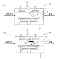
サセプタ2を所定のヒーター出力で加熱し、サセプタ2上をサセプタ温度測定用パイロメーター12で温度測定した場合、図2(a)に示すように、輻射光16は減衰されることがないため、表示される測定温度は正確なものとなる。
When the
しかし、サセプタ2とサセプタ温度測定用パイロメーター12との間の測定光路上に、ウォールデポ14が存在すると、サセプタ温度測定用パイロメーター12の輻射光16は減衰された輻射光16’となり、表示される測定温度が低くなる。したがって、前記チャンバー1内を昇温させ、ヒーター出力を一定に制御し、図2(a)のようにウォールデポの存在しない状態でのサセプタ2の温度を予め測定し、これを基準温度とする。
However, if there is a
次に、前記チャンバー1内を昇温させた状態での前記サセプタ温度が前記基準温度よりも低い場合には、図2(b)のようにウォールデポ14が生成されているものとみなして気相エッチングを開始する。基準温度が例えば1200℃であり、前記チャンバー1内を昇温させてもサセプタ温度が例えば1160℃にしか到達しないのであれば、ウォールデポが形成されていると考えられる。
Next, when the susceptor temperature in the state where the temperature in the
気相エッチングにあたっては、ヒーター出力を制御し、サセプタ2を例えば1200℃まで昇温する。前記サセプタ温度で例えば60秒間維持し、透明石英部材4,4’や不透明石英部材5,5’の温度を増加させる。続いて、ヒーター出力を一定に制御しながら、HClガスを例えば25slmチャンバー1に導入し、ウォールデポを除去する。
In the vapor phase etching, the heater output is controlled to raise the temperature of the
このようにして、チャンバー壁面のウォールデポが除去されるが、サセプタ温度が所定の基準温度となったときをエッチングの終点とする。その後、チャンバー1内を降温する。
In this way, the wall deposit on the chamber wall surface is removed, and when the susceptor temperature reaches a predetermined reference temperature is taken as the end point of the etching. Thereafter, the temperature inside the
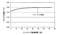
気相エッチングの経過時間とサセプタ温度の関係を示した例を図3に示す。図3に示した例では、エッチング開始後50秒間は透明石英部材4,4’上のウォールデポが除去されることにより、サセプタ温度の測定値が上昇するが、50秒以降は温度変化がなく、オーバーエッチングである。上述した本発明に係る気相エッチング方法のフローの例では、温度変化が1200℃となったときにエッチングを終了するため、過不足なくエッチングできる。また、従来は約70秒間気相エッチングを行っていたため、気相エッチングの時間が20秒間短縮されることとなる。
An example showing the relationship between the elapsed time of vapor phase etching and the susceptor temperature is shown in FIG. In the example shown in FIG. 3, the measured value of the susceptor temperature rises by removing the wall deposit on the
このように、本実施形態によれば、気相エッチング時にサセプタ温度測定用パイロメーター12でサセプタ表面温度を測定し、サセプタ温度が所定の値となった時をエッチングの終点とすることで、チャンバー1の透明石英部材4,4’上のウォールデポ上に付着するウォールデポを確実に除去することができる。また、チャンバー1内の部材上(サセプタ2の表面、透明石英部材4,4’の内壁、不透明石英部材5,5’の内壁)に生成されたウォールデポも除去されることとなる。
As described above, according to the present embodiment, the susceptor surface temperature is measured by the susceptor
本発明に係る気相エッチング方法では、従来よりも気相エッチング時間が短縮されるため、SiC部材へのエッチングによるダメージを低減し、生産性を向上することができる。 In the vapor phase etching method according to the present invention, since the vapor phase etching time is shortened compared to the conventional method, the damage to the SiC member due to the etching can be reduced, and the productivity can be improved.
また、上記した実施形態においては、サセプタ温度が所定の温度となったときにエッチングを終了する例を示したが、サセプタ温度が一定となるようにヒーター出力をフィードバック制御し、ヒーター出力が所定の値となった場合に前記サセプタ温度が前記基準温度となったとみなして気相エッチングを終了するようにしてもよい。 In the above embodiment, an example is described in which the etching is ended when the susceptor temperature reaches a predetermined temperature, but the heater output is feedback controlled so that the susceptor temperature becomes constant, and the heater output is predetermined. The gas phase etching may be ended assuming that the susceptor temperature has become the reference temperature when it reaches a value.
次に、本発明のエピタキシャル基板の製造方法について説明する。
まず、前述のように本発明の気相エッチング方法によってクリーニングされたチャンバー1を有するエピタキシャル成長装置13を用いて、基板搬入用ロボット(図示せず)などにより、エピタキシャル成長装置13のチャンバー1に、基板としてシリコン単結晶のウェーハWを搬入し、サセプタ2上に載置する。
Next, a method of manufacturing the epitaxial substrate of the present invention will be described.
First, using the
その後、前述したエピタキシャル層製造フローと同様にして、加熱装置であるヒーター10,10’によりウェーハWを例えば1100℃に昇温しながら原料ガスをチャンバー内に導入し、前記ウェーハの表面上にエピタキシャル層を形成し、エピタキシャルウェーハを製造する。これにより、ウェーハWの主表面上にシリコンエピタキシャル層が形成され、シリコンエピタキシャルウェーハを製造することができる。
Thereafter, the raw material gas is introduced into the chamber while raising the temperature of the wafer W to, for example, 1100 ° C. by the
1:チャンバー、2:サセプタ、3,3’:チャンバーベース、4,4’:透明石英部材、5,5’:不透明石英部材、6:サセプタ支持具、7:回転機構、8:気相成長ガス導入口、9:ガス排出口、10,10’:ヒーター、11:ウェーハ温度測定用パイロメーター、12:サセプタ温度測定用パイロメーター、13:気相成長装置、14:ウォールデポ、15:照射光、16:輻射光、16’:減衰された輻射光、W:ウェーハ。
1:
Claims (3)
前記チャンバーの外側に設けられ、測定光路が前記透明石英部材の内壁面上のウォールデポの生成が予測される箇所を横切って前記チャンバー内のサセプタ温度を測定するように設置されたサセプタ温度測定用パイロメーターと、を有する気相成長装置において実施される気相エッチング方法であり、
前記チャンバー内を昇温させ、前記ウォールデポの存在しない状態での前記サセプタ温度を予め測定することにより基準温度を設定しておく工程と、
前記チャンバー内を昇温させた状態での前記サセプタ温度が前記基準温度よりも低い場合には、前記ウォールデポが生成されているものとみなして気相エッチングを行う気相エッチング開始工程と、
前記サセプタ温度が前記基準温度となったら前記気相エッチングを終了する気相エッチング終了工程と、
を含む気相エッチング方法。 A susceptor on which a substrate is mounted, and a chamber in which the susceptor is accommodated and sealed by a transparent quartz member;
Susceptor temperature measurement, provided outside the chamber, for measuring the temperature of the susceptor in the chamber across a location where a measurement light path is expected to generate a wall deposit on the inner wall surface of the transparent quartz member A vapor phase etching method implemented in a vapor phase growth apparatus having a pyrometer,
Setting the reference temperature by raising the temperature in the chamber and measuring the susceptor temperature in the absence of the wall deposit in advance;
A vapor phase etching start step of performing vapor phase etching on the assumption that the wall deposit is generated when the susceptor temperature in a state where the temperature in the chamber is raised is lower than the reference temperature;
A vapor phase etching termination step of terminating the vapor phase etching when the susceptor temperature reaches the reference temperature;
Vapor phase etching method including:
Priority Applications (1)
| Application Number | Priority Date | Filing Date | Title |
|---|---|---|---|
| JP2016055179A JP6524944B2 (en) | 2016-03-18 | 2016-03-18 | Vapor phase etching method and epitaxial substrate manufacturing method |
Applications Claiming Priority (1)
| Application Number | Priority Date | Filing Date | Title |
|---|---|---|---|
| JP2016055179A JP6524944B2 (en) | 2016-03-18 | 2016-03-18 | Vapor phase etching method and epitaxial substrate manufacturing method |
Publications (2)
| Publication Number | Publication Date |
|---|---|
| JP2017168781A JP2017168781A (en) | 2017-09-21 |
| JP6524944B2 true JP6524944B2 (en) | 2019-06-05 |
Family
ID=59910261
Family Applications (1)
| Application Number | Title | Priority Date | Filing Date |
|---|---|---|---|
| JP2016055179A Active JP6524944B2 (en) | 2016-03-18 | 2016-03-18 | Vapor phase etching method and epitaxial substrate manufacturing method |
Country Status (1)
| Country | Link |
|---|---|
| JP (1) | JP6524944B2 (en) |
Families Citing this family (2)
| Publication number | Priority date | Publication date | Assignee | Title |
|---|---|---|---|---|
| JP7267843B2 (en) * | 2019-06-07 | 2023-05-02 | 株式会社アルバック | Plasma processing equipment |
| CN114397022B (en) * | 2022-01-28 | 2024-04-19 | 西安奕斯伟材料科技股份有限公司 | Method for calibrating thermometer of epitaxial furnace |
Family Cites Families (12)
| Publication number | Priority date | Publication date | Assignee | Title |
|---|---|---|---|---|
| WO1998001894A1 (en) * | 1996-07-03 | 1998-01-15 | Hitachi, Ltd. | Method of manufacturing semiconductor integrated circuit device |
| JP2933074B2 (en) * | 1998-01-06 | 1999-08-09 | 日本電気株式会社 | Vapor phase growth apparatus and cleaning method |
| JPH11345778A (en) * | 1998-05-29 | 1999-12-14 | Tokyo Electron Ltd | Method for cleaning film preparing apparatus and mechanism for cleaning the apparatus |
| JP3670533B2 (en) * | 1999-09-27 | 2005-07-13 | 株式会社東芝 | Substrate processing apparatus and cleaning method thereof |
| JP4806856B2 (en) * | 2001-03-30 | 2011-11-02 | 東京エレクトロン株式会社 | Heat treatment method and heat treatment apparatus |
| JP4391734B2 (en) * | 2002-09-26 | 2009-12-24 | 株式会社日立国際電気 | Manufacturing method of semiconductor device |
| US20050279384A1 (en) * | 2004-06-17 | 2005-12-22 | Guidotti Emmanuel P | Method and processing system for controlling a chamber cleaning process |
| WO2007041454A2 (en) * | 2005-10-03 | 2007-04-12 | Advanced Technology Materials, Inc. | Systems and methods for determination of endpoint of chamber cleaning processes |
| JP2008004603A (en) * | 2006-06-20 | 2008-01-10 | Toshiba Corp | Semiconductor manufacturing apparatus, and method of manufacturing the same |
| JP5750339B2 (en) * | 2011-08-31 | 2015-07-22 | 株式会社ニューフレアテクノロジー | Vapor phase growth method and vapor phase growth apparatus |
| JP5553066B2 (en) * | 2011-09-29 | 2014-07-16 | 信越半導体株式会社 | Epitaxial wafer manufacturing method |
| JP6360407B2 (en) * | 2014-10-02 | 2018-07-18 | グローバルウェーハズ・ジャパン株式会社 | Cleaning method of susceptor |
-
2016
- 2016-03-18 JP JP2016055179A patent/JP6524944B2/en active Active
Also Published As
| Publication number | Publication date |
|---|---|
| JP2017168781A (en) | 2017-09-21 |
Similar Documents
| Publication | Publication Date | Title |
|---|---|---|
| JP7175283B2 (en) | Integrated substrate temperature measurement on high temperature ceramic heaters | |
| TWI611043B (en) | Substrate processing apparatus, manufacturing method of semiconductor device, and recording medium | |
| JP5283370B2 (en) | Vapor growth apparatus and vapor growth method | |
| JP5158068B2 (en) | Vertical heat treatment apparatus and heat treatment method | |
| JP5661078B2 (en) | Method and apparatus for depositing a layer on a semiconductor wafer by vapor deposition in a processing chamber | |
| JP6599540B2 (en) | Reactor preparation method for manufacturing epitaxial wafers | |
| KR101422555B1 (en) | Vapor phase growing method and vapor phase growing apparatus | |
| JP6524944B2 (en) | Vapor phase etching method and epitaxial substrate manufacturing method | |
| JP2011165964A (en) | Method of manufacturing semiconductor device | |
| KR101086152B1 (en) | Cylinder for thermal processing chamber | |
| TW201600622A (en) | Cleaning method of apparatus for forming amorphous silicon film, and method and apparatus for forming amorphous silicon film | |
| US20160020086A1 (en) | Doping control methods and related systems | |
| JP2009147170A (en) | Method and device for manufacturing semiconductor device | |
| JP5719720B2 (en) | Thin film processing method | |
| JP5754651B2 (en) | Temperature adjusting method for vapor phase growth apparatus and epitaxial wafer manufacturing method | |
| KR101359548B1 (en) | Vapor phase growing method and vapor phase growing apparatus | |
| TW202301501A (en) | Method and reactor system for wafer temperature gradient control to suppress slip formation in high-temperature epitaxial film growth | |
| JP2004172409A (en) | Method for cleaning reaction vessel and film formation device | |
| JP2006339242A (en) | Manufacturing method of semiconductor device | |
| JP2004104014A (en) | Manufacturing method of semiconductor device | |
| JP7205455B2 (en) | Method for manufacturing epitaxial silicon wafer | |
| JP7439739B2 (en) | Temperature control method for epitaxial growth equipment and method for manufacturing silicon deposited layer wafer | |
| JP5807505B2 (en) | Epitaxial wafer manufacturing method | |
| CN111748788B (en) | Film forming method and film forming apparatus | |
| JP2008066558A (en) | Semiconductor manufacturing apparatus and semiconductor manufacturing method |
Legal Events
| Date | Code | Title | Description |
|---|---|---|---|
| A621 | Written request for application examination |
Free format text: JAPANESE INTERMEDIATE CODE: A621 Effective date: 20180319 |
|
| A131 | Notification of reasons for refusal |
Free format text: JAPANESE INTERMEDIATE CODE: A131 Effective date: 20190122 |
|
| A521 | Request for written amendment filed |
Free format text: JAPANESE INTERMEDIATE CODE: A523 Effective date: 20190306 |
|
| TRDD | Decision of grant or rejection written | ||
| A01 | Written decision to grant a patent or to grant a registration (utility model) |
Free format text: JAPANESE INTERMEDIATE CODE: A01 Effective date: 20190409 |
|
| A61 | First payment of annual fees (during grant procedure) |
Free format text: JAPANESE INTERMEDIATE CODE: A61 Effective date: 20190422 |
|
| R150 | Certificate of patent or registration of utility model |
Ref document number: 6524944 Country of ref document: JP Free format text: JAPANESE INTERMEDIATE CODE: R150 |
|
| R250 | Receipt of annual fees |
Free format text: JAPANESE INTERMEDIATE CODE: R250 |
|
| R250 | Receipt of annual fees |
Free format text: JAPANESE INTERMEDIATE CODE: R250 |