JP6520480B2 - Coil parts - Google Patents
Coil parts Download PDFInfo
- Publication number
- JP6520480B2 JP6520480B2 JP2015131267A JP2015131267A JP6520480B2 JP 6520480 B2 JP6520480 B2 JP 6520480B2 JP 2015131267 A JP2015131267 A JP 2015131267A JP 2015131267 A JP2015131267 A JP 2015131267A JP 6520480 B2 JP6520480 B2 JP 6520480B2
- Authority
- JP
- Japan
- Prior art keywords
- coil
- resin
- substrate
- winding portion
- resin wall
- Prior art date
- Legal status (The legal status is an assumption and is not a legal conclusion. Google has not performed a legal analysis and makes no representation as to the accuracy of the status listed.)
- Active
Links
- 229920005989 resin Polymers 0.000 claims description 122
- 239000011347 resin Substances 0.000 claims description 122
- 238000004804 winding Methods 0.000 claims description 93
- 239000000758 substrate Substances 0.000 claims description 65
- 238000007747 plating Methods 0.000 claims description 21
- 239000006247 magnetic powder Substances 0.000 claims description 10
- 239000002184 metal Substances 0.000 description 9
- 229910052751 metal Inorganic materials 0.000 description 9
- 239000012212 insulator Substances 0.000 description 8
- 238000004519 manufacturing process Methods 0.000 description 5
- 239000000463 material Substances 0.000 description 5
- 239000011248 coating agent Substances 0.000 description 4
- 238000000576 coating method Methods 0.000 description 4
- 239000010949 copper Substances 0.000 description 4
- 238000009413 insulation Methods 0.000 description 4
- 229910052802 copper Inorganic materials 0.000 description 3
- 238000000034 method Methods 0.000 description 3
- RYGMFSIKBFXOCR-UHFFFAOYSA-N Copper Chemical compound [Cu] RYGMFSIKBFXOCR-UHFFFAOYSA-N 0.000 description 2
- 239000000853 adhesive Substances 0.000 description 2
- 230000001070 adhesive effect Effects 0.000 description 2
- 230000015556 catabolic process Effects 0.000 description 2
- 239000004020 conductor Substances 0.000 description 2
- 239000007772 electrode material Substances 0.000 description 2
- 239000011521 glass Substances 0.000 description 2
- 239000000126 substance Substances 0.000 description 2
- JYEUMXHLPRZUAT-UHFFFAOYSA-N 1,2,3-triazine Chemical compound C1=CN=NN=C1 JYEUMXHLPRZUAT-UHFFFAOYSA-N 0.000 description 1
- XQUPVDVFXZDTLT-UHFFFAOYSA-N 1-[4-[[4-(2,5-dioxopyrrol-1-yl)phenyl]methyl]phenyl]pyrrole-2,5-dione Chemical compound O=C1C=CC(=O)N1C(C=C1)=CC=C1CC1=CC=C(N2C(C=CC2=O)=O)C=C1 XQUPVDVFXZDTLT-UHFFFAOYSA-N 0.000 description 1
- XEEYBQQBJWHFJM-UHFFFAOYSA-N Iron Chemical compound [Fe] XEEYBQQBJWHFJM-UHFFFAOYSA-N 0.000 description 1
- 229910001030 Iron–nickel alloy Inorganic materials 0.000 description 1
- 239000004642 Polyimide Substances 0.000 description 1
- 229910045601 alloy Inorganic materials 0.000 description 1
- 239000000956 alloy Substances 0.000 description 1
- 239000004760 aramid Substances 0.000 description 1
- 229920003235 aromatic polyamide Polymers 0.000 description 1
- 239000000919 ceramic Substances 0.000 description 1
- 229910052804 chromium Inorganic materials 0.000 description 1
- 239000011651 chromium Substances 0.000 description 1
- XLJMAIOERFSOGZ-UHFFFAOYSA-M cyanate Chemical compound [O-]C#N XLJMAIOERFSOGZ-UHFFFAOYSA-M 0.000 description 1
- 230000007423 decrease Effects 0.000 description 1
- 230000000694 effects Effects 0.000 description 1
- 238000005516 engineering process Methods 0.000 description 1
- 239000003822 epoxy resin Substances 0.000 description 1
- 239000004744 fabric Substances 0.000 description 1
- 230000004907 flux Effects 0.000 description 1
- 229910052737 gold Inorganic materials 0.000 description 1
- 239000010931 gold Substances 0.000 description 1
- 239000011810 insulating material Substances 0.000 description 1
- 239000000696 magnetic material Substances 0.000 description 1
- 239000000203 mixture Substances 0.000 description 1
- 229910052759 nickel Inorganic materials 0.000 description 1
- PXHVJJICTQNCMI-UHFFFAOYSA-N nickel Substances [Ni] PXHVJJICTQNCMI-UHFFFAOYSA-N 0.000 description 1
- 230000003647 oxidation Effects 0.000 description 1
- 238000007254 oxidation reaction Methods 0.000 description 1
- 230000000149 penetrating effect Effects 0.000 description 1
- 229910000889 permalloy Inorganic materials 0.000 description 1
- 238000000206 photolithography Methods 0.000 description 1
- 238000005498 polishing Methods 0.000 description 1
- 229920003192 poly(bis maleimide) Polymers 0.000 description 1
- 229920000647 polyepoxide Polymers 0.000 description 1
- 229920001721 polyimide Polymers 0.000 description 1
- 229910000702 sendust Inorganic materials 0.000 description 1
- 229910000679 solder Inorganic materials 0.000 description 1
- 229920001187 thermosetting polymer Polymers 0.000 description 1
- 229910052718 tin Inorganic materials 0.000 description 1
- 239000011135 tin Substances 0.000 description 1
Images


Classifications
-
- H—ELECTRICITY
- H01—ELECTRIC ELEMENTS
- H01F—MAGNETS; INDUCTANCES; TRANSFORMERS; SELECTION OF MATERIALS FOR THEIR MAGNETIC PROPERTIES
- H01F27/00—Details of transformers or inductances, in general
- H01F27/28—Coils; Windings; Conductive connections
- H01F27/32—Insulating of coils, windings, or parts thereof
- H01F27/323—Insulation between winding turns, between winding layers
-
- H—ELECTRICITY
- H01—ELECTRIC ELEMENTS
- H01F—MAGNETS; INDUCTANCES; TRANSFORMERS; SELECTION OF MATERIALS FOR THEIR MAGNETIC PROPERTIES
- H01F17/00—Fixed inductances of the signal type
- H01F17/0006—Printed inductances
- H01F17/0013—Printed inductances with stacked layers
-
- H—ELECTRICITY
- H01—ELECTRIC ELEMENTS
- H01F—MAGNETS; INDUCTANCES; TRANSFORMERS; SELECTION OF MATERIALS FOR THEIR MAGNETIC PROPERTIES
- H01F27/00—Details of transformers or inductances, in general
- H01F27/28—Coils; Windings; Conductive connections
- H01F27/2804—Printed windings
-
- H—ELECTRICITY
- H01—ELECTRIC ELEMENTS
- H01F—MAGNETS; INDUCTANCES; TRANSFORMERS; SELECTION OF MATERIALS FOR THEIR MAGNETIC PROPERTIES
- H01F27/00—Details of transformers or inductances, in general
- H01F27/28—Coils; Windings; Conductive connections
- H01F27/32—Insulating of coils, windings, or parts thereof
- H01F27/324—Insulation between coil and core, between different winding sections, around the coil; Other insulation structures
Description
本発明は、コイル部品に関する。 The present invention relates to a coil component.
従来、表面実装型の平面コイル素子等のコイル部品が、民生用機器、産業用機器等の電気製品に幅広く利用されている。中でも小型携帯機器においては、機能の充実化に伴い、各々のデバイスを駆動させるために単一の電源から複数の電圧を得る必要が生じてきている。そこで、このような電源用途等にも表面実装型の平面コイル素子が使用されている。 2. Description of the Related Art Conventionally, coil components such as surface-mounted flat coil elements are widely used in electric products such as consumer devices and industrial devices. Above all, in the case of small portable devices, it is necessary to obtain a plurality of voltages from a single power source to drive each device as the functions are enhanced. Then, the surface mounting type planar coil element is used also for such a power supply application etc.
このようなコイル部品は、たとえば、下記特許文献1に開示されている。この文献に開示されたコイル部品は、基板の表裏面にそれぞれ平面渦巻き状の空芯コイルが設けられ、空芯コイルの磁芯部分において基板を貫くように設けられたスルーホール導体により空芯コイル同士が接続されている。
Such a coil component is disclosed, for example, in
上述した空芯コイルは、基板上に設けられたシードパターンに、Cuなどの導体材料をめっき成長させることで形成されるが、基板の面方向へのめっき成長によりコイルの巻回部の間隔が狭まる。コイルの巻回部の間隔が狭い場合には、コイルの絶縁性低下が懸念されるため、より確実に絶縁する技術が望まれている。 The air core coil described above is formed by plating and growing a conductive material such as Cu on a seed pattern provided on the substrate, but the plating growth in the surface direction of the substrate causes the distance between the winding portions of the coil to It narrows. In the case where the distance between the winding portions of the coil is narrow, there is a concern that the insulation of the coil may deteriorate, and therefore, a technique for more reliable insulation is desired.
そこで、コイルの隣り合う巻回部の間に樹脂壁を設けて確実な絶縁を図る技術の開発が進められている。ただし、樹脂壁が基板と別体で設けられる場合には、樹脂壁と基板との接合面はその他の箇所に比べて耐圧が低くなることが考えられる。そのため、巻回部の間における高い絶縁耐圧を実現するためには、上記接合面おける耐圧の向上が求められる。 Therefore, development of technology for achieving reliable insulation by providing a resin wall between adjacent winding portions of a coil has been advanced. However, in the case where the resin wall is provided separately from the substrate, it is conceivable that the pressure resistance of the bonding surface between the resin wall and the substrate is lower than that at other portions. Therefore, in order to realize a high dielectric breakdown voltage between the winding parts, improvement of the breakdown voltage at the joint surface is required.
本発明は、上述の課題を解決するためになされたものであり、巻回部の間の耐圧向上が図られたコイル部品を提供することを目的とする。 The present invention was made in order to solve the above-mentioned subject, and an object of the present invention is to provide a coil component in which pressure resistance improvement between winding parts was aimed at.
本発明の一側面に係るコイル部品は、基板と、基板の主面上にめっき成長で設けられたコイルと、基板の主面上に設けられ、コイルの巻回部が間に延びる複数の樹脂壁を有する樹脂体と、磁性粉含有樹脂からなり、基板の主面のコイルと樹脂体とを一体的に覆う被覆樹脂とを備え、巻回部が、樹脂壁の下端部が基板の主面と接合される接合面から離間している。 A coil component according to one aspect of the present invention is provided on a substrate, a coil provided by plating growth on the main surface of the substrate, and a plurality of resins provided on the main surface of the substrate, with the coil winding portion extending therebetween A resin body having a wall, and a covering resin made of a magnetic powder-containing resin and integrally covering the coil of the main surface of the substrate and the resin body, the lower end portion of the resin wall of the winding portion is the main surface of the substrate It is separated from the joint surface to be joined.
このようなコイル部品においては、樹脂壁の下端部と基板の主面との接合面から巻回部が離間しているために、樹脂壁を介して隣り合う巻回部同士が接合面付近において遠ざかっている。それにより、上記接合面を介しての短絡が抑制されることで、巻回部の間の耐圧向上が図られている。 In such a coil component, since the winding portion is separated from the bonding surface between the lower end portion of the resin wall and the main surface of the substrate, the winding portions adjacent to each other via the resin wall are in the vicinity of the bonding surface I am away. Thereby, the withstand voltage improvement between winding parts is achieved by the short circuit via the said joint surface being suppressed.
また、巻回部と接合面との間に空隙が存在し、該空隙を介して、巻回部が接合面から離間している態様であってもよい。 In addition, an air gap may be present between the winding portion and the bonding surface, and the winding portion may be separated from the bonding surface via the air gap.
また、空隙は、巻回部の下に入り込むくさび部を含む断面形状を有している態様であってもよい。 Also, the air gap may be in a form having a cross-sectional shape including a wedge portion which gets under the winding portion.
また、樹脂体の樹脂壁の断面形状が四角形状である態様であってもよい。このとき、樹脂体の樹脂壁の断面は底辺の長さに対する高さの比が1より大きく、該樹脂壁が基板の主面の法線方向に沿って長く延びている態様であってもよい。 Moreover, the aspect whose cross-sectional shape of the resin wall of a resin body is square shape may be sufficient. At this time, the cross section of the resin wall of the resin body may have an aspect in which the ratio of the height to the length of the base is larger than 1 and the resin wall extends long along the normal direction of the main surface of the substrate. .
また、コイルの巻回部の断面形状が四角形状である態様であってもよい。このとき、コイルの巻回部の断面は底辺の長さに対する高さの比が1より大きく、該巻回部の断面が基板の主面の法線方向に沿って長く延びている態様であってもよい。 Moreover, the cross-sectional shape of the winding part of a coil may be a square-shaped aspect. At this time, the section of the winding portion of the coil has a ratio of the height to the length of the base greater than 1, and the cross section of the winding portion is elongated along the normal direction of the main surface of the substrate. May be
また、樹脂体の樹脂壁の高さがコイルの巻回部の高さより高い態様であってもよい。この場合、巻回部は、高さ方向にわたって設計寸法どおりの厚さとなり得る。また、巻回部同士が樹脂壁を越えて接する事態が有意に回避される。 Further, the height of the resin wall of the resin body may be higher than the height of the winding portion of the coil. In this case, the winding portion can have a thickness as designed over the height direction. Moreover, the situation in which the wound portions contact with each other beyond the resin wall is significantly avoided.
また、樹脂体は、基板の主面上にコイルがめっき成長される前に設けられ、コイルの巻回部は、樹脂体の樹脂壁に接着されていない態様であってもよい。 The resin body may be provided before the coil is plated and grown on the main surface of the substrate, and the winding portion of the coil may not be bonded to the resin wall of the resin body.
また、基板の主面上に複数並んだ樹脂壁のうち、最外に位置する樹脂壁の厚さが内側に位置する樹脂壁の厚さより厚い態様であってもよい。 In addition, of the plurality of resin walls arranged on the main surface of the substrate, the thickness of the resin wall positioned outermost may be thicker than the thickness of the resin wall positioned inside.
本発明によれば、巻回部の間の耐圧向上が図られたコイル部品が提供される。 According to the present invention, there is provided a coil component in which the withstand voltage between the winding portions is improved.
以下、添付図面を参照して、本発明の実施形態について詳細に説明する。なお、説明において、同一要素又は同一機能を有する要素には、同一符号を用いることとし、重複する説明は省略する。 Hereinafter, embodiments of the present invention will be described in detail with reference to the accompanying drawings. In the description, the same elements or elements having the same function will be denoted by the same reference symbols, without redundant description.
まず、本発明の実施形態に係るコイル部品の構造について、図1〜4を参照しつつ説明する。説明の便宜上、図示のようにXYZ座標を設定する。すなわち、平面コイル素子の厚さ方向をZ方向、外部端子電極の対面方向をY方向、Z方向とY方向とに直交する方向をX方向と設定する。 First, the structure of a coil component according to an embodiment of the present invention will be described with reference to FIGS. For convenience of explanation, XYZ coordinates are set as illustrated. That is, the thickness direction of the planar coil element is set as the Z direction, the facing direction of the external terminal electrode is set as the Y direction, and the direction orthogonal to the Z direction and the Y direction is set as the X direction.
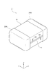
コイル部品1は、略直方体形状を呈する本体部10と、本体部10の対向する一対の端面を覆うようにして設けられた一対の外部端子電極30A、30Bとによって構成されている。コイル部品1は、一例として、長辺2.0mm、短辺1.6mm、高さ0.9mmの寸法で設計される。
The
以下では、本体部10を作製する手順を示しつつ、併せて、コイル部品1の構造についても説明する。
Below, the structure of the
本体部10は、図2に示す基板11を含んでいる。基板11は、非磁性の絶縁材料で構成された平板矩形状の部材である。基板11の中央部分には、主面11a、11b間を繋ぐように貫通された略円形の開口12が設けられている。基板11としては、ガラスクロスにシアネート樹脂(BT(ビスマレイミド・トリアジン)レジン:登録商標)が含浸された基板で、板厚60μmのものを用いることができる。なお、BTレジンのほか、ポリイミド、アラミド等を用いることもできる。基板11の材料としては、セラミックやガラスを用いることもできる。基板11の材料としては、大量生産されているプリント基板材料が好ましく、特にBTプリント基板、FR4プリント基板、あるいはFR5プリント基板に用いられる樹脂材料が最も好ましい。
The
基板11には、図3に示すように、それぞれの主面11a、11bに、後述するコイル13をめっき成長させるためのシードパターン13Aが形成されている。シードパターン13Aは、基板11の開口12の周りを回る螺旋パターン14Aと、基板11のY方向に関する端部に形成された端部パターン15Aとを有し、これらのパターン14A、15Aが連続的かつ一体的に形成されている。なお、一方の主面11a側に設けられるコイル13と他方の主面11b側に設けられるコイル13とでは電極引き出し方向が逆であり、そのため、一方の主面11a側の端部パターン15Aと他方の主面11b側の端部パターンとは、基板11のY方向に関する互いに異なる端部に形成されている。
As shown in FIG. 3, a
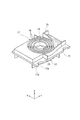
図2に戻って、基板11の各主面11a、11b上には、樹脂体17が設けられている。樹脂体17は、公知のフォトリソグラフィーによってパターニングされた厚膜レジストである。樹脂体17は、コイル13の巻回部14の成長領域を画定する樹脂壁18と、コイル13の引出電極部15の成長領域を画定する樹脂壁19とを有している。
Returning to FIG. 2,
図4は、シードパターン13Aを用いてコイル13をめっき成長させたときの基板11の状態を示している。コイル13のめっき成長には、公知のめっき成長方法を採用することができる。
FIG. 4 shows the state of the
コイル13は、銅で構成されており、シードパターン13Aの螺旋パターン14A上に形成された巻回部14と、シードパターン13Aの端部パターン15A上に形成された引出電極部15とを有している。コイル13は、平面視したときに、シードパターン13A同様、基板11の主面11a、11bに平行に延在する平面渦巻き状の空芯コイルの形状となっている。より詳しくは、基板上面11aの巻回部14は、上面側から見て外側に向かう方向に沿って左回転の渦巻きであり、基板下面11bの巻回部14は、下面側から見て、外側に向かう方向に沿って左回転の渦巻きである。基板上面11aおよび基板下面11bの両コイル13は、たとえば、開口12の近傍に別途設けられた貫通孔を介して端部同士が接続される。両コイル13に一方向に電流を流したときには、両コイル13の電流の流れる回転方向が同一となるため、コイル13で発生する磁束が重畳して強め合う。
The
図5は、図4に示しためっき成長後の基板11の状態を示しており、図4のV−V線断面図である。
FIG. 5 shows the state of the
図5に示すように、基板11上には、基板11の法線方向(Z方向)に沿って長く延びる四角形状断面(図5では矩形状断面)の樹脂壁18が形成されており、これらの樹脂壁18の間においてコイル13の巻回部14がZ方向に成長する。コイル13の巻回部14は、その成長領域が、めっき成長前に基板11上に形成された樹脂壁18によって予め画定されている。
As shown in FIG. 5, on the
コイル13の巻回部14は、螺旋パターン14Aの一部であるシード部14aと、シード部14a上にめっき成長させためっき部14bとで構成されており、シード部14a周りにめっき部14bが徐々に成長していくことにより形成される。このとき、コイル13の巻回部14は、隣り合う2つの樹脂壁18の間に画成された空間を充たすように成長して、樹脂壁18の間に画成された空間と同一の形状に形成され、その結果、コイル13の巻回部14は基板11の法線方向(Z方向)に沿って長く延びる四角形状断面(図5では矩形状断面)となる。すなわち、樹脂壁18の間に画成される空間の形状を調整することで、コイル13の巻回部14の形状が調整され、設計したとおりの形状にコイル13の巻回部14を形成することができる。
The winding
コイル13の巻回部14は、隣り合う2つの樹脂壁18の間を成長する際、成長領域を画定する樹脂壁18の内側面に接しながら成長していく。このとき、コイル13の巻回部14と樹脂壁18との間には、機械的結合も化学的結合も生じない。すなわち、コイル13の巻回部14は、樹脂壁18と接着されないままめっき成長し、非接着状態で樹脂壁18の間に介在する。本明細書において「非接着状態」とは、アンカー効果等の機械的結合および共有結合等の化学的結合が生じていない状態をいう。
When the winding
コイル13の巻回部14の断面寸法は、一例として、高さ80〜260μm、幅(厚さ)40〜260μm、下端部の幅(底辺)に対する高さの比(アスペクト比)1〜5である。コイル13の巻回部14のアスペクト比は2〜5であってもよい。
The cross-sectional dimension of the winding
図5に示すとおり、コイル13の巻回部14の高さhは、樹脂壁18の高さHよりも低いこと(h<H)が好ましい。すなわち、コイル13の巻回部14のめっき成長が樹脂壁18の高さHよりも低い位置で止まるように調整することが好ましい。コイル13の巻回部14の高さhが樹脂壁18の高さHよりも低いと、巻回部14は高さ方向にわたって設計寸法どおりの厚さとなる。また、コイル13の巻回部14の高さhが、樹脂壁18の高さHより高いと、隣り合う巻回部14同士が接触したり後述する絶縁体40や接合層41の厚さを十分に確保できなくなったりする事態が生じ、コイル13の耐圧抵抗が低下するためである。
As shown in FIG. 5, it is preferable that the height h of the winding
また、コイル13の巻回部14の厚さDは、高さ方向にわたって均一になっている。これは、隣り合う樹脂壁18の間隔が高さ方向にわたって均一になっているためである。
Further, the thickness D of the winding
さらに、図5に示すように、コイル13の巻回部14の上面14cは、上側に突き出た形状となっている。より詳しくは、コイル13の巻回部14の上面14cは、中央部では基板11の主面11aに対して略平行になっているが、樹脂壁18近傍の端部では曲線状に漸次下降している。そして、コイル13の巻回部14の上面14cにおいては、基板11の主面11aに対する相対位置に関し、上面14cの樹脂壁18と接する高さ位置が、上面14cの中央部に位置する最高の高さ位置よりも低くなっている。
Furthermore, as shown in FIG. 5, the
なお、図5に示した態様では、各樹脂壁18の厚さd1、d2も、コイル13の巻回部14同様、高さ方向にわたって均一となっている。その結果、隣り合うコイル13の巻回部14の間隔が、高さ方向にわたって均一になる。すなわち、コイル13の巻回部14は、高さ方向に関して局所的に薄くなっている箇所(つまり、局所的に耐圧抵抗が低下している箇所)が存在しない、または存在しにくい構造となっている。樹脂壁18の断面寸法は、一例として、高さ50〜300μm、幅(厚さ)5〜30μm、下端部の幅(底辺)に対する高さの比(アスペクト比)5〜30である。樹脂壁18の断面寸法は、高さ180〜300μm、幅(厚さ)5〜12μm、アスペクト比15〜30であってもよい。
In the embodiment shown in FIG. 5, the thicknesses d1 and d2 of the
図6に示すように、樹脂壁18は、基板11とは別体に設けられており、その下端面18aは基板11の主面11aと接して接合面Sを形成している。接合面S付近には、空隙Gが形成されており、巻回部14が接合面Sおよび樹脂壁18の下端部から離間している。換言すると、巻回部14は、巻回部14と接合面Sとの間に存在する空隙Gを介して、接合面Sから離間している。
As shown in FIG. 6, the
空隙Gの断面形状は、図6に示したように、基板11の主面11aに沿って巻回部14の下に入り込むように延び、かつ、樹脂壁18の側面に沿って上方に延びた形状とすることができる。この場合、空隙Gは、巻回部14の下に入り込むくさび部gを含む断面形状を有する。空隙Gの断面形状は、接合面Sに対応する角が直角である直角三角形に近い形状とすることができる。空隙Gは、巻回部14をめっき成長により形成する際のめっき条件やめっき液の組成等を調整し、たとえば幅方向への成長を抑制することで容易に得ることができる。
The cross-sectional shape of the air gap G extends along the
また、樹脂壁18によって画成された空間は、上端が開放されており、樹脂壁18の上端部が巻回部14の上側を覆うように回り込んでいないため、巻回部14の上側の設計自由度が高い。すなわち、巻回部14の上に任意の層を形成する態様も何の層も形成しない態様も選択し得る。
The space defined by the
巻回部14の上に層を形成する場合には、各種の層形態や層材料を選択し得る。たとえば、図7に示すように、巻回部14の上に、後述する被覆樹脂21に含まれる金属磁性粉と巻回部14との間の絶縁性を高めるために、絶縁体40を設けることができる。絶縁体40は、絶縁樹脂または絶縁磁性材料で構成することができる。また、絶縁体40は、巻回部14の上面14cに直接的または間接的に接するとともに、巻回部14と樹脂壁18とを一体的に覆っている。なお、絶縁体40は、巻回部14のみを選択的に覆う構成にすることもできる。また、巻回部14と絶縁体40との間の接合性を高めるために、所定の接合層(たとえば、酸化による銅めっきの黒化層)41を設けることができる。
When forming a layer on the winding
さらに、図5に示すとおり、複数の樹脂壁18のうち、最外に位置する樹脂壁18の厚さd1が内側に位置する樹脂壁18の厚さd2より厚いこと(d1>d2)が好ましい。この場合、コイル部品1の作製時や使用時に受けるZ方向の圧力に対して剛性が付与される。厚さが厚い樹脂壁18を最外位置に配置することで、この部分において主に上記圧力を受け止める。剛性の観点からは、両端に位置する樹脂壁18の両方が、内側に位置する樹脂壁18の厚さより厚いことが好ましい。
Furthermore, as shown in FIG. 5, it is preferable that the thickness d1 of the
なお、上述したコイル13のめっき成長は、基板11の両主面11a、11bにおいておこなわれる。両主面11a、11bのコイル13同士は、基板11の開口においてそれぞれの端部同士が接続されて導通される。
The plating growth of the
基板11上にコイル13をめっき成長させた後、図8に示すように、基板11は被覆樹脂21で全体的に覆われる。すなわち、被覆樹脂21が、基板11の主面11a、11bのコイル13と樹脂体17とを一体的に覆う。樹脂体17は、被覆樹脂21内に残ったままコイル部品1の一部を構成する。被覆樹脂21は、金属磁性粉含有樹脂からなり、ウエハ状態の基板11の上に形成され、その後、硬化されることにより形成される。
After plating and growing the
被覆樹脂21を構成する金属磁性粉含有樹脂は、金属磁性粉が分散された樹脂で構成されている。金属磁性粉は、たとえば鉄ニッケル合金(パーマロイ合金)、カルボニル鉄、アモルファス、非晶質または結晶質のFeSiCr系合金、センダスト等で構成され得る。金属磁性粉含有樹脂に用いられる樹脂は、たとえば熱硬化性のエポキシ樹脂である。金属磁性粉含有樹脂に含まれる金属磁性粉の含有量は、一例として、90〜99wt%である。
The metal magnetic powder-containing resin constituting the covering
さらに、ダイシングしてチップ化することで、図9に示す本体部10が得られる。チップ化した後、必要に応じてバレル研磨等によりエッジの面取りをおこなってもよい。
Furthermore, by dicing into chips, the
最後に、本体部10の端部パターン15Aが露出した端面(Y方向において対向する端面)に、端部パターン15Aと電気的に接続されるように外部端子電極30A、30Bを設けることで、コイル部品1が完成する。外部端子電極30A、30Bは、コイル部品を搭載する基板の回路に接続するための電極であり、複数層構造とすることができる。たとえば、外部端子電極30A、30Bは、端面に樹脂電極材料を塗布した後、その樹脂電極材料に金属めっきを施すことにより形成することができる。外部端子電極30A、30Bの金属めっきには、Cr、Cu、Ni、Sn、Au、はんだ等を用いることができる。
Finally, the external
上述したコイル部品1によれば、樹脂壁18の下端部と基板11の主面11aとの接合面Sから巻回部14が離間しているために、樹脂壁18を介して隣り合う巻回部14同士が接合面S付近において遠ざかっている。これは、接合面Sを介して短絡するモードを考えたときに、隣り合う巻回部14同士の距離(すなわち、沿面距離)は、巻回部14同士が接合面S付近において遠ざかっていない(すなわち、空隙Gが存在しない)場合に比べて、延長されていることを意味している。それにより、接合面Sを介しての短絡が抑制され、その結果、巻回部14の間の耐圧向上が実現されている。
According to the
その上、巻回部14が接合面Sから離間していることで、接合面Sの間にめっきが浸入して、耐圧が低下してしまう事態も生じにくくなっている。
Moreover, since the winding
特に、空隙Gが、巻回部14の下に入り込むくさび部gを含む断面形状を有する場合には、隣り合う巻回部14同士の距離がさらに延長されるため、さらなる耐圧向上が実現される。
In particular, when the air gap G has a cross-sectional shape including the wedge portion g which enters under the winding
また、コイル部品1によれば、コイル13の巻回部14の上面14cが樹脂壁18と接する高さ位置が、上面14cにおける最高の高さ位置よりも低くなっている。そのため、巻回部14から、樹脂壁18を介して隣り合う巻回部14までの沿面距離の延長が図られており、隣り合う巻回部14の間において耐圧が向上している。
Further, according to the
さらに、コイル部品1によれば、複数の樹脂壁18の間にコイル13の巻回部14が非接着状態で介在するため、コイル13の巻回部14と樹脂壁18とが互いに対して変位可能である。そのため、コイル部品1の使用環境が高温になったときなどの周辺温度に変化があり、コイル13の巻回部14と樹脂壁18との間の熱膨張係数の差に起因する応力が生じた場合であっても、コイル13の巻回部14と樹脂壁18とが相対移動することでその応力が緩和される。
Furthermore, according to the
また、コイル部品1の製造方法によれば、樹脂体17の樹脂壁18の間に介在するように、コイル13の巻回部14がめっき成長されている。すなわち、被覆樹脂21でコイル13を覆う前に、コイル13の巻回部14間にはすでに樹脂壁18が介在している。そのため、コイル13の巻回部14間に樹脂を別途に充填する必要はなく、樹脂壁18によりコイル13の巻回部14間の樹脂の寸法精度の安定化が図られる。
Further, according to the method of manufacturing the
1…コイル部品、11…基板、13…コイル、14…巻回部、14a…シード部、14b…めっき部、14c…上面、17…樹脂体、18…樹脂壁、18a…下端面、21…被覆樹脂、30A、30B…外部端子電極、40…絶縁体、G…空隙、g…くさび部、S…接合面。
DESCRIPTION OF
Claims (10)
前記基板の主面上にめっき成長で設けられたコイルと、
前記基板の主面上に設けられ、前記コイルの巻回部が間に延びる複数の樹脂壁を有する樹脂体と、
磁性粉含有樹脂からなり、前記基板の主面の前記コイルと前記樹脂体とを一体的に覆う被覆樹脂と
を備え、
前記巻回部が、前記樹脂壁の下端部が前記基板の主面と接合される接合面から離間している、コイル部品。 A substrate,
A coil provided by plating growth on the main surface of the substrate;
A resin body having a plurality of resin walls provided on the main surface of the substrate and in which the winding portion of the coil extends therebetween;
And a covering resin made of a magnetic powder-containing resin and integrally covering the coil on the main surface of the substrate and the resin body,
The coil component, wherein the winding portion is separated from a joint surface where the lower end of the resin wall is joined to the main surface of the substrate.
Priority Applications (2)
| Application Number | Priority Date | Filing Date | Title |
|---|---|---|---|
| JP2015131267A JP6520480B2 (en) | 2015-06-30 | 2015-06-30 | Coil parts |
| KR1020160080509A KR101846150B1 (en) | 2015-06-30 | 2016-06-28 | Coil component |
Applications Claiming Priority (1)
| Application Number | Priority Date | Filing Date | Title |
|---|---|---|---|
| JP2015131267A JP6520480B2 (en) | 2015-06-30 | 2015-06-30 | Coil parts |
Publications (2)
| Publication Number | Publication Date |
|---|---|
| JP2017017141A JP2017017141A (en) | 2017-01-19 |
| JP6520480B2 true JP6520480B2 (en) | 2019-05-29 |
Family
ID=57811397
Family Applications (1)
| Application Number | Title | Priority Date | Filing Date |
|---|---|---|---|
| JP2015131267A Active JP6520480B2 (en) | 2015-06-30 | 2015-06-30 | Coil parts |
Country Status (2)
| Country | Link |
|---|---|
| JP (1) | JP6520480B2 (en) |
| KR (1) | KR101846150B1 (en) |
Families Citing this family (1)
| Publication number | Priority date | Publication date | Assignee | Title |
|---|---|---|---|---|
| KR20210097260A (en) | 2020-01-29 | 2021-08-09 | 삼성디스플레이 주식회사 | Apparatus and method for manufacturing a display apparatus |
Family Cites Families (5)
| Publication number | Priority date | Publication date | Assignee | Title |
|---|---|---|---|---|
| JP4191506B2 (en) | 2003-02-21 | 2008-12-03 | Tdk株式会社 | High density inductor and manufacturing method thereof |
| JP3914173B2 (en) | 2003-05-29 | 2007-05-16 | 新科實業有限公司 | Thin film coil and method for forming the same, thin film magnetic head and method for manufacturing the same |
| JP2005210010A (en) | 2004-01-26 | 2005-08-04 | Tdk Corp | Coil substrate, manufacturing method thereof, and surface-mounting coil element |
| JP2006135056A (en) | 2004-11-05 | 2006-05-25 | Shinko Electric Ind Co Ltd | Plane balun built in printed board and its manufacturing method |
| JP6312997B2 (en) * | 2013-07-31 | 2018-04-18 | 新光電気工業株式会社 | Coil substrate, manufacturing method thereof, and inductor |
-
2015
- 2015-06-30 JP JP2015131267A patent/JP6520480B2/en active Active
-
2016
- 2016-06-28 KR KR1020160080509A patent/KR101846150B1/en active IP Right Grant
Also Published As
| Publication number | Publication date |
|---|---|
| KR20170003434A (en) | 2017-01-09 |
| JP2017017141A (en) | 2017-01-19 |
| KR101846150B1 (en) | 2018-04-06 |
Similar Documents
| Publication | Publication Date | Title |
|---|---|---|
| KR102401620B1 (en) | Coil component and method for manufacturing the same | |
| JP6716865B2 (en) | Coil parts | |
| KR102264363B1 (en) | Coil forming substrate and method for manufacturing the same | |
| JP6429609B2 (en) | Coil component and manufacturing method thereof | |
| JP6716866B2 (en) | Coil parts | |
| JP6716867B2 (en) | Coil component and manufacturing method thereof | |
| JP6477262B2 (en) | Coil parts | |
| JP6447368B2 (en) | Coil parts | |
| JP6879355B2 (en) | Manufacturing method of coil parts | |
| JP6520480B2 (en) | Coil parts | |
| JP6428204B2 (en) | Coil component and manufacturing method thereof | |
| JP6428203B2 (en) | Coil component and manufacturing method thereof | |
| US20220189679A1 (en) | Coil component | |
| JP2019033282A (en) | Coil component and manufacturing method thereof |
Legal Events
| Date | Code | Title | Description |
|---|---|---|---|
| A621 | Written request for application examination |
Free format text: JAPANESE INTERMEDIATE CODE: A621 Effective date: 20180411 |
|
| A977 | Report on retrieval |
Free format text: JAPANESE INTERMEDIATE CODE: A971007 Effective date: 20190117 |
|
| A131 | Notification of reasons for refusal |
Free format text: JAPANESE INTERMEDIATE CODE: A131 Effective date: 20190129 |
|
| A521 | Written amendment |
Free format text: JAPANESE INTERMEDIATE CODE: A523 Effective date: 20190320 |
|
| TRDD | Decision of grant or rejection written | ||
| A01 | Written decision to grant a patent or to grant a registration (utility model) |
Free format text: JAPANESE INTERMEDIATE CODE: A01 Effective date: 20190402 |
|
| A61 | First payment of annual fees (during grant procedure) |
Free format text: JAPANESE INTERMEDIATE CODE: A61 Effective date: 20190415 |
|
| R150 | Certificate of patent or registration of utility model |
Ref document number: 6520480 Country of ref document: JP Free format text: JAPANESE INTERMEDIATE CODE: R150 |