JP6509435B2 - Ethernet bus, controller, and method for waking up Ethernet bus controller - Google Patents
Ethernet bus, controller, and method for waking up Ethernet bus controller Download PDFInfo
- Publication number
- JP6509435B2 JP6509435B2 JP2018516781A JP2018516781A JP6509435B2 JP 6509435 B2 JP6509435 B2 JP 6509435B2 JP 2018516781 A JP2018516781 A JP 2018516781A JP 2018516781 A JP2018516781 A JP 2018516781A JP 6509435 B2 JP6509435 B2 JP 6509435B2
- Authority
- JP
- Japan
- Prior art keywords
- voltage
- bus
- control device
- control
- circuit
- Prior art date
- Legal status (The legal status is an assumption and is not a legal conclusion. Google has not performed a legal analysis and makes no representation as to the accuracy of the status listed.)
- Active
Links
- 230000002618 waking effect Effects 0.000 title claims description 8
- 238000000034 method Methods 0.000 title claims description 7
- 239000003990 capacitor Substances 0.000 claims description 13
- 238000004891 communication Methods 0.000 claims description 5
- 230000008878 coupling Effects 0.000 description 3
- 238000010168 coupling process Methods 0.000 description 3
- 238000005859 coupling reaction Methods 0.000 description 3
- 230000005540 biological transmission Effects 0.000 description 2
- 230000000903 blocking effect Effects 0.000 description 2
- 238000010586 diagram Methods 0.000 description 2
- 230000001419 dependent effect Effects 0.000 description 1
- 238000005516 engineering process Methods 0.000 description 1
- 230000001105 regulatory effect Effects 0.000 description 1
Images
Classifications
-
- H—ELECTRICITY
- H04—ELECTRIC COMMUNICATION TECHNIQUE
- H04L—TRANSMISSION OF DIGITAL INFORMATION, e.g. TELEGRAPHIC COMMUNICATION
- H04L12/00—Data switching networks
- H04L12/28—Data switching networks characterised by path configuration, e.g. LAN [Local Area Networks] or WAN [Wide Area Networks]
- H04L12/40—Bus networks
- H04L12/40006—Architecture of a communication node
- H04L12/40039—Details regarding the setting of the power status of a node according to activity on the bus
-
- G—PHYSICS
- G06—COMPUTING; CALCULATING OR COUNTING
- G06F—ELECTRIC DIGITAL DATA PROCESSING
- G06F13/00—Interconnection of, or transfer of information or other signals between, memories, input/output devices or central processing units
- G06F13/38—Information transfer, e.g. on bus
- G06F13/40—Bus structure
- G06F13/4063—Device-to-bus coupling
- G06F13/4068—Electrical coupling
-
- G—PHYSICS
- G06—COMPUTING; CALCULATING OR COUNTING
- G06F—ELECTRIC DIGITAL DATA PROCESSING
- G06F1/00—Details not covered by groups G06F3/00 - G06F13/00 and G06F21/00
- G06F1/26—Power supply means, e.g. regulation thereof
- G06F1/32—Means for saving power
- G06F1/3203—Power management, i.e. event-based initiation of a power-saving mode
- G06F1/3234—Power saving characterised by the action undertaken
- G06F1/3296—Power saving characterised by the action undertaken by lowering the supply or operating voltage
-
- H—ELECTRICITY
- H04—ELECTRIC COMMUNICATION TECHNIQUE
- H04L—TRANSMISSION OF DIGITAL INFORMATION, e.g. TELEGRAPHIC COMMUNICATION
- H04L12/00—Data switching networks
- H04L12/02—Details
- H04L12/12—Arrangements for remote connection or disconnection of substations or of equipment thereof
-
- H—ELECTRICITY
- H04—ELECTRIC COMMUNICATION TECHNIQUE
- H04L—TRANSMISSION OF DIGITAL INFORMATION, e.g. TELEGRAPHIC COMMUNICATION
- H04L12/00—Data switching networks
- H04L12/28—Data switching networks characterised by path configuration, e.g. LAN [Local Area Networks] or WAN [Wide Area Networks]
- H04L12/40—Bus networks
- H04L12/40006—Architecture of a communication node
- H04L12/40013—Details regarding a bus controller
-
- H—ELECTRICITY
- H04—ELECTRIC COMMUNICATION TECHNIQUE
- H04L—TRANSMISSION OF DIGITAL INFORMATION, e.g. TELEGRAPHIC COMMUNICATION
- H04L12/00—Data switching networks
- H04L12/28—Data switching networks characterised by path configuration, e.g. LAN [Local Area Networks] or WAN [Wide Area Networks]
- H04L12/40—Bus networks
- H04L2012/40267—Bus for use in transportation systems
- H04L2012/40273—Bus for use in transportation systems the transportation system being a vehicle
-
- Y—GENERAL TAGGING OF NEW TECHNOLOGICAL DEVELOPMENTS; GENERAL TAGGING OF CROSS-SECTIONAL TECHNOLOGIES SPANNING OVER SEVERAL SECTIONS OF THE IPC; TECHNICAL SUBJECTS COVERED BY FORMER USPC CROSS-REFERENCE ART COLLECTIONS [XRACs] AND DIGESTS
- Y02—TECHNOLOGIES OR APPLICATIONS FOR MITIGATION OR ADAPTATION AGAINST CLIMATE CHANGE
- Y02D—CLIMATE CHANGE MITIGATION TECHNOLOGIES IN INFORMATION AND COMMUNICATION TECHNOLOGIES [ICT], I.E. INFORMATION AND COMMUNICATION TECHNOLOGIES AIMING AT THE REDUCTION OF THEIR OWN ENERGY USE
- Y02D30/00—Reducing energy consumption in communication networks
- Y02D30/50—Reducing energy consumption in communication networks in wire-line communication networks, e.g. low power modes or reduced link rate
Landscapes
- Engineering & Computer Science (AREA)
- Theoretical Computer Science (AREA)
- Signal Processing (AREA)
- Computer Networks & Wireless Communication (AREA)
- General Engineering & Computer Science (AREA)
- Physics & Mathematics (AREA)
- General Physics & Mathematics (AREA)
- Computer Hardware Design (AREA)
- Small-Scale Networks (AREA)
- Direct Current Feeding And Distribution (AREA)
- Semiconductor Integrated Circuits (AREA)
- Dc Digital Transmission (AREA)
- Power Sources (AREA)
Description
本発明は、イーサネットバス、制御装置、および、イーサネットバスの制御装置をウェイクアップする方法に関する。 The present invention relates to an Ethernet bus, a controller, and a method of waking up a controller of the Ethernet bus.
バスシステム、特に車両ネットワークにおける制御装置は、好ましくは、その機能が必要となったときのみ活性化すべきである。機能が必要でないときには、こうした制御装置を不活性化すべきであり、大きな必要エネルギを有するべきでない。ネットワーク技術であるCANおよびFlexRayにおいては、有効な信号がバス上に生じるとただちに、制御装置の電圧制御回路をスイッチオンする、特別に起動可能なバスドライバが規定されている。イーサネットバスシステムにおいては、これまでこうした規格が存在していなかった。 The control system in the bus system, in particular in the vehicle network, should preferably be activated only when its function is required. When functions are not required, such controls should be deactivated and not have a large required energy. In the network technologies CAN and FlexRay, a specially bootable bus driver is defined which switches on the voltage control circuit of the control device as soon as a valid signal is present on the bus. In Ethernet bus systems, such a standard has not existed until now.
ここで、既に、2つのデータ線路またはバス線路に差動信号としての起動信号を印加することが提案されている。これは、正規の通信信号に相当する交流電圧信号であってよいし、または、直流電圧であってもよい。ただし、起動信号を印加および検出する回路は、対称性ひいては伝送特性に負の影響を与えかねない。 Here, it has already been proposed to apply a start signal as a differential signal to two data lines or bus lines. This may be an AC voltage signal corresponding to a regular communication signal, or may be a DC voltage. However, the circuit that applies and detects the start signal may negatively affect the symmetry and thus the transmission characteristics.
本発明の基礎とする技術的課題は、対称性への影響なしに制御装置をウェイクアップ可能なイーサネットバスおよび制御装置を提供し、さらに、イーサネットバスの制御装置のウェイクアップ方法を利用することができるようにすることである。 The technical problem on which the present invention is based is to provide an Ethernet bus and controller capable of waking up the controller without affecting the symmetry, and to use the method of waking up the controller of the Ethernet bus. It is to be able to do it.
この技術的課題を解決する手段は、請求項1の特徴を有するイーサネットバス、請求項7の特徴を有する制御装置、および、請求項8の特徴を有する方法によって得られる。本発明のさらに有利な実施形態は、各従属請求項から得られる。
Means for solving this technical problem are obtained by an Ethernet bus having the features of claim 1, a control device having the features of claim 7, and a method having the features of
イーサネットバスは、少なくとも2つの制御装置を含む。この場合の制御装置は、スイッチであってもよい。各制御装置は、それぞれ1つずつバスドライバとマイクロプロセッサとを有し、ここで、少なくとも第1の制御装置は、この制御装置の動作電圧に対する少なくとも2つの電圧値を調整可能な電圧制御回路を有する。ここで、第1の電圧値は、動作状態「スリープ」または不活性状態に対して設けられており、第2の電圧値は、動作状態「通信」もしくは「ウェイク」または活性状態に対して設けられている。バスドライバは、それぞれ、少なくとも2つのバス線路を介して相互に接続されている。バス線路には、各制御装置の要素であるそれぞれ1つずつのターミネーションネットワークが接続されている。ターミネーションネットワークは、少なくとも2つの抵抗と1つのキャパシタとを有し、ここで、2つの抵抗は、それぞれ1つずつのバス線路に接続されており、かつ、ターミネーションネットワークの中間タップで相互に接続されており、ターミネーションネットワークのキャパシタは、中間タップとアースとの間に配置されている。イーサネットバスは、ウェイクアップイベントに依存して、電圧制御回路によって制御装置の中間タップの電圧を変化させるための電圧信号を形成するように構成された少なくとも1つのウェイクアップモジュールを有する。この場合、少なくとも1つの電圧制御回路には、中間タップの電圧に依存して電圧制御回路を第1の電圧値から第2の電圧値へ制御する回路、すなわち、電圧制御回路をウェイクアップまたは起動する回路が設けられている。この場合、データ伝送の対称性は、影響を受けない。この場合、ウェイクアップモジュールの出力端の電圧は、予め定められた時間だけ生じればよく、その後で再び遮断することができるように構成可能である。このとき、電圧制御回路は、調整された第2の電圧値にとどめられるか、または、制御装置が活性状態にあるかぎり、ウェイクアップモジュールの出力端の電圧を持続的に印加される。 The Ethernet bus includes at least two controllers. The control device in this case may be a switch. Each controller has one bus driver and one microprocessor, wherein at least the first controller controls the voltage control circuit capable of adjusting at least two voltage values with respect to the operating voltage of the controller. Have. Here, the first voltage value is provided for the operating state "sleep" or the inactive state, and the second voltage value is provided for the operating state "communication" or "wake" or the active state. It is done. The bus drivers are mutually connected via at least two bus lines. One termination network, which is an element of each control device, is connected to the bus line. The termination network has at least two resistors and one capacitor, where the two resistors are each connected to one bus line and are mutually connected by the middle taps of the termination network The capacitor of the termination network is located between the middle tap and the ground. The Ethernet bus has at least one wakeup module configured to form a voltage signal for changing the voltage of the control unit's middle tap by the voltage control circuit depending on the wakeup event. In this case, at least one voltage control circuit is a circuit that controls the voltage control circuit from the first voltage value to the second voltage value depending on the voltage of the intermediate tap, ie, wakes up or starts the voltage control circuit. Circuits are provided. In this case, the symmetry of the data transmission is not affected. In this case, the voltage at the output of the wakeup module need only be generated for a predetermined time, and can be configured to be able to shut off again after that. At this time, the voltage control circuit is continuously applied with the voltage of the output of the wakeup module as long as the regulated second voltage value is maintained or the controller is in an active state.
一実施形態においては、第2の制御装置も2つの電圧値を有する電圧制御回路を有し、この電圧制御回路に、電圧制御回路に対する中間タップの電圧を評価する回路が設けられる。このようにすれば、第2の制御装置も不活性化させ、第1の制御装置のウェイクアップにより、これに連動して自動的にウェイクアップさせることができる。なぜなら、第1の制御装置の中間タップの電圧の変化が、バス線路を介して、他方の制御装置の中間タップの電圧も変化させるからである。 In one embodiment, the second control device also has a voltage control circuit with two voltage values, which is provided with a circuit for evaluating the voltage of the intermediate tap relative to the voltage control circuit. In this way, the second control device can also be inactivated, and wakeup of the first control device can automatically wake up in conjunction with this. This is because the change in voltage of the middle tap of the first control device also changes the voltage of the middle tap of the other control device via the bus line.
別の実施形態においては、第2の制御装置もウェイクアップモジュールを有する。 In another embodiment, the second controller also has a wakeup module.
さらに別の実施形態においては、ウェイクアップモジュールおよび/または回路が制御装置に組み込まれる。 In yet another embodiment, a wakeup module and / or circuitry is incorporated into the controller.
さらに別の実施形態においては、回路は、分圧器を形成する抵抗とトランジスタとを有する。ここで、電圧制御回路の制御入力端は、分圧器の中間タップに接続され、分圧器は、動作電圧とアースとの間に配置され、トランジスタの制御入力端は、ターミネーションネットワークの中間タップに接続される。このようにすれば、ウェイクアップモジュールがトランジスタを導通切り換えすることができ、これにより、分圧器の中間タップの電圧が変化し、よって、電圧制御回路が切り換えられる。なお、ここで、例えばウェイクアップモジュールの電圧がトランジスタを阻止する逆のロジックも可能であることに注意されたい。この場合、回路の動作電圧を制御装置の動作電圧と等しくする必要はない。 In yet another embodiment, the circuit comprises a resistor and a transistor forming a voltage divider. Here, the control input of the voltage control circuit is connected to the middle tap of the voltage divider, the voltage divider is arranged between the operating voltage and ground, and the control input of the transistor is connected to the middle tap of the termination network Be done. In this way, the wake-up module can switch on the transistor, which changes the voltage of the middle tap of the voltage divider and thus switches the voltage control circuit. It should be noted here that the reverse logic is also possible, for example the voltage of the wakeup module blocking the transistor. In this case, the operating voltage of the circuit does not have to be equal to the operating voltage of the control device.
さらに別の実施形態においては、高周波コモンモード干渉を抑制するために、ウェイクアップモジュールに少なくとも1つのフィルタが設けられる。例えば、このために、ウェイクアップモジュールの出力端にチョークまたはローパスが配置される。これにより、コモンモード干渉による制御装置の誤ったウェイクアップが防止される。入力ノイズを抑制するために、ウェイクアップモジュールの入力端にローパスを設けてもよい。 In yet another embodiment, the wakeup module is provided with at least one filter to suppress high frequency common mode interference . For example, for this purpose a choke or low pass is arranged at the output of the wakeup module. This prevents false wakeup of the controller due to common mode interference . A low pass may be provided at the input of the wakeup module to suppress input noise.
好ましい適用分野は、自動車での使用である。 A preferred field of application is the use in motor vehicles.
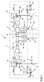
本発明を以下に好ましい実施例に則して詳細に説明する。唯一の図には、イーサネットバスの一部の概略的なブロック図が示されている。 The invention will now be described in detail by way of a preferred embodiment. The sole figure shows a schematic block diagram of part of the Ethernet bus.
図1には、第1の制御装置2と第2の制御装置3とを有するイーサネットバス1が示されている。制御装置2,3は、それぞれ1つずつバスドライバ4とマイクロプロセッサ5とを有しており、ここで、各バスドライバ4は、少なくとも2つのバス線路6,7によって相互に接続されている。2つの制御装置2,3は、それぞれ、2つの抵抗R1,R2と1つのキャパシタC3とから成るターミネーションネットワーク8を有する。この場合、それぞれ、抵抗R1は、バス線路6に接続されており、抵抗R2は、バス線路7に接続されており、2つの抵抗は、ターミネーションネットワーク8の中間タップ9で相互に接続されている。中間タップ9とアースとの間に、キャパシタC3が配置されている。また、2つの制御装置2,3は、カップリングキャパシタC1,C2を有しており、各カップリングキャパシタC1,C2は、バス線路6,7に接続されており、かつ、バス線路6,7とバスドライバとの間に位置している。ここでは、第2の制御装置3のカップリングキャパシタC1,C2は示されていない。さらに、制御装置2,3はコモンモードチョークCMCを有しており、同様に、ここでは、第2の制御装置3のチョークは示されていない。制御装置2,3は、それぞれ、第1の動作電圧VBATを制御装置2,3の動作電圧VCCに変換する電圧制御回路10を有する。この場合、動作電圧VCCは、スイッチオフ可能(第1の電圧値)またはスイッチオン可能(第2の電圧値)である。電圧制御回路10には、抵抗RおよびトランジスタTを有する回路11が設けられており、この回路11は、動作電圧VBATとアースとの間に直列に配置されている。回路11は、分圧器を形成しており、中間タップ12は、電圧制御回路10の制御入力端13に接続されている。トランジスタTの制御入力端14は、ターミネーションネットワーク8の中間タップ9に接続されている。さらに、制御装置2,3はそれぞれ、動作電圧VBATを出力電圧へ変換するウェイクアップモジュール15を有しており、この出力電圧がチョークLを介して中間タップ9にかかる。この場合、ウェイクアップモジュール15は、ウェイクアップイベントSに依存して出力電圧を導通切り換えする制御入力端16を有しており、ここで、制御入力端16の前方には、さらにローパス17が配置されていてもよい。
FIG. 1 shows an Ethernet bus 1 having a
不活性状態では、トランジスタTは阻止状態にあるので、近似的には、VBATが電圧制御回路10の制御入力端13にかかる。制御装置2をウェイクアップする場合、信号Sが制御入力端16に印加され、これにより、ウェイクアップモジュール15の出力電圧が中間タップ9にかかり、その電位が持ち上げられる。したがって、制御入力端14によりトランジスタTがオンへ制御される。これにより、動作電圧VBATが抵抗Rを介して降下し、制御入力端13がアースへ引かれる。ここから、マイクロプロセッサ5およびバスドライバ4のための動作電圧VCCが生じる(第2の電圧値)。制御装置2の中間タップ9の電位の上昇は、バス線路6,7を介して第2の制御装置3の中間タップ9へ伝送されるので、ここでも同様に、電圧制御回路10がスイッチオンされる。
In the inactive state, since the transistor T is in the blocking state, approximately V BAT is applied to the
Claims (8)
前記少なくとも2つの制御装置(2,3)は、それぞれ1つずつのバスドライバ(4)とマイクロプロセッサ(5)とを有し、
前記少なくとも2つの制御装置(2,3)は、少なくとも、第1の制御装置(2)及び第2の制御装置(3)を含み、
少なくとも前記第1の制御装置(2)は、当該第1の制御装置(2)の動作電圧(VCC)に対する少なくとも2つの電圧値を調整可能な電圧制御回路(10)を有し、ここで、前記少なくとも2つの電圧値のうちの第1の電圧値は、動作状態「スリープ」に対して設けられており、前記少なくとも2つの電圧値のうちの第2の電圧値は、動作状態「通信」に対して設けられており、
前記第1の制御装置(2)のバスドライバ(4)と前記第2の制御装置(3)のバスドライバ(4)とは、互いに、少なくとも2つのバス線路(6,7)を介して接続されており、
前記少なくとも2つのバス線路(6,7)には、それぞれが少なくとも2つの抵抗(R1,R2)と1つのキャパシタ(C3)とを有する、2つのターミネーションネットワーク(8)が接続されており、
前記2つのターミネーションネットワーク(8)の前記2つの抵抗(R1,R2)のうちの第1の抵抗(R1)は、前記少なくとも2つのバス線路(6,7)のうちの第1のバス線路(6)と接続されており、前記2つのターミネーションネットワーク(8)の前記2つの抵抗(R1,R2)のうちの第2の抵抗(R2)は、前記少なくとも2つのバス線路(6,7)のうちの第2のバス線路(7)と接続されており、かつ、前記第1の抵抗(R1)と前記第2の抵抗(R2)とは、前記2つのターミネーションネットワーク(8)のそれぞれの中間タップ(9)で相互に接続されており、
前記2つのターミネーションネットワーク(8)のそれぞれの前記キャパシタ(C3)は、前記中間タップ(9)とアースとの間に配置されている、
イーサネットバス(1)において、
前記イーサネットバス(1)は、ウェイクアップイベント(S)に依存して、前記電圧制御回路(10)によって前記第1の制御装置(2)の前記中間タップ(9)の電圧を変化させるための電圧信号を形成するように構成された少なくとも1つのウェイクアップモジュール(15)を有し、
少なくとも1つの前記電圧制御回路(10)には、前記中間タップ(9)の電圧に依存して前記電圧制御回路(10)を前記第1の電圧値から前記第2の電圧値へ制御する回路(11)が設けられている、
ことを特徴とするイーサネットバス(1)。 An Ethernet bus (1) comprising at least two control devices (2, 3),
The at least two control devices (2, 3) each have a bus driver (4) and a microprocessor (5).
The at least two control devices (2, 3) include at least a first control device (2) and a second control device (3).
At least said first control device (2) comprises a voltage control circuit (10) capable of adjusting at least two voltage values with respect to the operating voltage (V CC ) of said first control device (2), The first voltage value of the at least two voltage values is provided for the operating state “sleep”, and the second voltage value of the at least two voltage values is the operating state “communication Provided for
The bus driver (4) of the first control device (2) and the bus driver (4) of the second control device (3) are connected to each other via at least two bus lines (6, 7) Has been
Two termination networks (8) are connected to the at least two bus lines (6, 7), each having at least two resistors (R1, R2) and one capacitor (C3),
A first resistance (R1) of the two resistances (R1, R2) of the two termination networks (8) is a first bus line of the at least two bus lines (6, 7) 6), and the second resistor (R2) of the two resistors (R1, R2) of the two termination networks (8) is connected to the at least two bus lines (6, 7) The first resistance (R1) and the second resistance (R2) are connected to the second bus line (7) of the two, and are respectively intermediate between the two termination networks (8). Mutually connected with tap (9),
The capacitor (C3) of each of the two termination networks (8) is disposed between the middle tap (9) and ground.
In the Ethernet bus (1)
The Ethernet bus (1) is for changing the voltage of the middle tap (9) of the first control device (2) by the voltage control circuit (10) depending on the wakeup event (S). Having at least one wakeup module (15) configured to form a voltage signal;
A circuit for controlling the voltage control circuit (10) from the first voltage value to the second voltage value depending on the voltage of the intermediate tap (9) in at least one of the voltage control circuits (10) (11) is provided,
Ethernet bus characterized by (1).
前記電圧制御回路(10)に対する前記中間タップ(9)の電圧を評価する回路(11)が設けられている、
請求項1に記載のイーサネットバス(1)。 The second control unit (3) likewise has a voltage control circuit (10) having two voltage values,
A circuit (11) is provided for evaluating the voltage of the intermediate tap (9) to the voltage control circuit (10),
An Ethernet bus (1) according to claim 1.
請求項1または2に記載のイーサネットバス(1)。 The first control device (2) and the second control device (3) are each provided with a wakeup module (15).
An Ethernet bus (1) according to claim 1 or 2.
請求項1から3までのいずれか1項に記載のイーサネットバス(1)。 Said wakeup module (15) is integrated in the control device (2, 3),
An Ethernet bus (1) according to any one of claims 1 to 3.
前記電圧制御回路(10)の制御入力端(13)は、前記分圧器の中間タップ(12)に接続されており、
前記分圧器は、動作電圧(VBAT)とアースとの間に配置されており、
前記トランジスタ(T)の制御入力端(14)は、前記ターミネーションネットワーク(8)の前記中間タップ(9)に接続されている、
請求項1から4までのいずれか1項に記載のイーサネットバス(1)。 The circuit (11) comprises a resistor (R) forming a voltage divider and a transistor (T).
The control input (13) of the voltage control circuit (10) is connected to the middle tap (12) of the voltage divider,
The voltage divider is located between the operating voltage (V BAT ) and ground,
The control input (14) of the transistor (T) is connected to the middle tap (9) of the termination network (8),
An Ethernet bus (1) according to any one of the preceding claims.
請求項1から5までのいずれか1項に記載のイーサネットバス(1)。 The wakeup module (15) is provided with at least one filter (L, 17) to suppress high frequency common mode interference ,
An Ethernet bus (1) according to any one of the preceding claims.
前記電圧制御回路(10)は、前記制御装置(2,3)の動作電圧(VCC)に対する少なくとも2つの電圧値を有し、ここで、前記少なくとも2つの電圧値のうちの第1の電圧値は、動作状態「スリープ」に対して設けられており、前記少なくとも2つの電圧値のうちの第2の電圧値は、動作状態「通信」に対して設けられており、
前記制御装置(2,3)は、少なくとも2つの抵抗(R1,R2)と1つのキャパシタ(C3)とを有するターミネーションネットワーク(8)を有しており、
前記少なくとも2つの抵抗(R1,R2)のうちの第1の抵抗(R1)は、2つのバス線路(6,7)のうちの第1のバス線路(6)への端子に接続されており、前記少なくとも2つの抵抗(R1,R2)のうちの第2の抵抗(R2)は、前記2つのバス線路(6,7)のうちの第2のバス線路(7)への端子に接続されており、
前記2つの抵抗(R1,R2)は、中間タップ(9)で相互に接続されており、
前記キャパシタ(C3)は、前記中間タップ(9)とアースとの間に配置されている、
制御装置(2,3)において、
前記制御装置(2,3)は、ウェイクアップイベント(S)に依存して、前記中間タップ(9)の電圧を変化させるための電圧信号を形成するように構成されており、かつ、前記ウェイクアップイベント(S)のための入力端(16)と前記ターミネーションネットワーク(8)の前記中間タップ(9)への出力端とを有するウェイクアップモジュール(15)を有しており、
前記電圧制御回路(10)には、前記中間タップ(9)の電圧に依存して前記電圧制御回路(10)を前記第1の電圧値から前記第2の電圧値へ制御する回路(11)が設けられており、
前記ウェイクアップイベント(S)に依存して前記入力端(16)に信号が入力されると、前記ウェイクアップモジュール(15)の出力電圧が前記中間タップ(9)にかかるため、前記中間タップ(9)の電圧が上昇し、前記回路(11)は、前記中間タップ(9)の電圧の上昇に依存して、前記電圧制御回路(10)を前記第1の電圧値から前記第2の電圧値へ制御する、
ことを特徴とする制御装置(2,3)。 A controller (2, 3) for an Ethernet bus (1), comprising a bus driver (4), a microprocessor (5) and a voltage control circuit (10),
The voltage control circuit (10) has at least two voltage values with respect to the operating voltage (V CC ) of the control device (2, 3), wherein the first voltage of the at least two voltage values A value is provided for the operating state "sleep", and a second voltage value of the at least two voltage values is provided for the operating state "communication",
The control device (2, 3) comprises a termination network (8) comprising at least two resistors (R1, R2) and one capacitor (C3),
The first resistance (R1) of the at least two resistances (R1, R2) is connected to the terminal to the first bus line (6) of the two bus lines (6, 7) A second resistor (R2) of the at least two resistors (R1, R2) is connected to a terminal to a second bus line (7) of the two bus lines (6, 7) Yes,
The two resistors (R1, R2) are mutually connected by an intermediate tap (9),
The capacitor (C3) is disposed between the middle tap (9) and ground.
In the control device (2, 3),
The control device (2, 3) is configured to form a voltage signal for changing the voltage of the intermediate tap (9) in dependence on a wake up event (S), and the wake and have a wake-up module (15) having said output terminal to the intermediate tap (9) of the input end (16) and the termination network (8) for up event (S),
The voltage control circuit (10) is a circuit (11) that controls the voltage control circuit (10) from the first voltage value to the second voltage value depending on the voltage of the intermediate tap (9). Is provided,
When a signal is input to the input terminal (16) depending on the wakeup event (S), the output voltage of the wakeup module (15) is applied to the intermediate tap (9). 9), the circuit (11) increases the voltage control circuit (10) from the first voltage value to the second voltage depending on the increase in voltage of the middle tap (9). Control to the value,
A control device (2, 3) characterized in that.
前記制御装置(2,3)は、バスドライバ(4)と、マイクロプロセッサ(5)と、前記制御装置(2,3)の動作電圧(VCC)に対する少なくとも2つの電圧値を調整可能な電圧制御回路(10)とを有し、ここで、第1の電圧値は、動作状態「スリープ」に対して設けられており、第2の電圧値は、動作状態「通信」に対して設けられており、
前記バスドライバ(4)は、少なくとも2つのバス線路(6,7)に接続されており、
前記バス線路(6,7)には、少なくとも2つの抵抗(R1,R2)と1つのキャパシタ(C3)とを有するターミネーションネットワーク(8)が接続されており、
前記2つの抵抗(R1,R2)は、それぞれ1つずつのバス線路(6,7)に接続されており、かつ、前記ターミネーションネットワーク(8)の中間タップ(9)で相互に接続されており、
前記ターミネーションネットワーク(8)の前記キャパシタ(C3)は、前記中間タップ(9)とアースとの間に配置されている、
制御装置をウェイクアップする方法において、
ウェイクアップイベント(S)に依存して、前記中間タップ(9)の電圧を変化させるための電圧信号を形成するウェイクアップモジュール(15)が設けられており、
回路(11)を介して、前記中間タップ(9)での当該電圧変化が検出され、前記電圧制御回路(10)が前記第1の電圧値から前記第2の電圧値へ制御される、
ことを特徴とする制御装置をウェイクアップする方法。
A method of waking up a control device (2, 3) of an Ethernet bus (1), comprising:
The control device (2, 3) can adjust at least two voltage values with respect to the operating voltage (V CC ) of the bus driver (4), the microprocessor (5), and the control device (2, 3). A control circuit (10), wherein a first voltage value is provided for the operating state "sleep" and a second voltage value is provided for the operating state "communication" Yes,
The bus driver (4) is connected to at least two bus lines (6, 7),
A termination network (8) having at least two resistors (R1, R2) and one capacitor (C3) is connected to the bus lines (6, 7),
The two resistors (R1 and R2) are respectively connected to one bus line (6, 7), and are mutually connected by an intermediate tap (9) of the termination network (8). ,
The capacitor (C3) of the termination network (8) is disposed between the middle tap (9) and ground.
In the method of waking up the control device
There is provided a wakeup module (15) which forms a voltage signal for changing the voltage of said intermediate tap (9) in dependence on the wakeup event (S).
The voltage change at the intermediate tap (9) is detected via the circuit (11), and the voltage control circuit (10) is controlled from the first voltage value to the second voltage value.
A method of waking up a control device characterized in that.
Applications Claiming Priority (3)
| Application Number | Priority Date | Filing Date | Title |
|---|---|---|---|
| DE102015222112.1 | 2015-11-10 | ||
| DE102015222112.1A DE102015222112A1 (en) | 2015-11-10 | 2015-11-10 | Ethernet bus, controller and method for waking up a controller of an Ethernet bus |
| PCT/EP2016/075380 WO2017080792A1 (en) | 2015-11-10 | 2016-10-21 | Ethernet bus, controller and method for waking a controller of an ethernet bus |
Publications (3)
| Publication Number | Publication Date |
|---|---|
| JP2018535588A JP2018535588A (en) | 2018-11-29 |
| JP2018535588A5 JP2018535588A5 (en) | 2019-04-25 |
| JP6509435B2 true JP6509435B2 (en) | 2019-05-08 |
Family
ID=57249777
Family Applications (1)
| Application Number | Title | Priority Date | Filing Date |
|---|---|---|---|
| JP2018516781A Active JP6509435B2 (en) | 2015-11-10 | 2016-10-21 | Ethernet bus, controller, and method for waking up Ethernet bus controller |
Country Status (7)
| Country | Link |
|---|---|
| US (1) | US10700887B2 (en) |
| EP (1) | EP3375136B1 (en) |
| JP (1) | JP6509435B2 (en) |
| KR (1) | KR101947972B1 (en) |
| CN (1) | CN108352993B (en) |
| DE (1) | DE102015222112A1 (en) |
| WO (1) | WO2017080792A1 (en) |
Families Citing this family (3)
| Publication number | Priority date | Publication date | Assignee | Title |
|---|---|---|---|---|
| US11832184B2 (en) * | 2018-12-13 | 2023-11-28 | Lg Electronics Inc. | System and method for exchanging data or signals for vehicle |
| CN111490918B (en) * | 2019-01-29 | 2021-07-30 | 广州汽车集团股份有限公司 | Vehicle-mounted Ethernet network awakening system, method and device and computer equipment |
| CN113993196B (en) * | 2021-10-25 | 2024-01-30 | 浙江吉利控股集团有限公司 | Node control method, system, equipment and storage medium of vehicle-mounted Ethernet |
Family Cites Families (21)
| Publication number | Priority date | Publication date | Assignee | Title |
|---|---|---|---|---|
| DE19611945C1 (en) * | 1996-03-26 | 1997-11-20 | Daimler Benz Ag | Device for the bus-connected operation of an electronic device with a microcontroller and its use |
| JP2003143044A (en) * | 2001-10-31 | 2003-05-16 | Matsushita Electric Ind Co Ltd | Two-wire power multiplex communication system, master unit thereof and two-wire power multiplex communication method |
| US6747498B1 (en) * | 2002-12-20 | 2004-06-08 | Texas Instruments Incorporated | CAN receiver wake-up circuit |
| DE10358584A1 (en) * | 2002-12-30 | 2004-07-15 | Robert Bosch Gmbh | Waking of bus members in sleep mode, especially for application to a motor vehicle CAN bus system, whereby the time interval between signal flanks on the bus system is measured and a corresponding bus member activated |
| US7779451B2 (en) | 2006-03-30 | 2010-08-17 | Intel Corporation | Securing wakeup network events |
| US8156353B2 (en) * | 2007-09-17 | 2012-04-10 | Intel Corporation | Techniques for communications power management based on system states |
| DE102008002946B4 (en) * | 2008-07-16 | 2010-04-08 | Lear Corporation Gmbh | Method for detecting an error on a data line |
| CN101482734B (en) | 2009-01-22 | 2011-11-30 | 深圳市博孚机电有限公司 | Low-power consumption control circuit and its operating procedure |
| DE102009015197A1 (en) | 2009-03-31 | 2010-10-14 | Volkswagen Ag | Vehicle network control unit and method for operating a vehicle network |
| EP2309677B1 (en) * | 2009-10-06 | 2012-09-05 | Nxp B.V. | Wake up detector for a bus transceiver |
| EP2339790A1 (en) | 2009-12-28 | 2011-06-29 | Nxp B.V. | Definition of wakeup bus messages for partial networking |
| DE102010049835A1 (en) * | 2010-10-27 | 2012-05-03 | Volkswagen Ag | Network and method for operating a network |
| CN101977162B (en) * | 2010-12-03 | 2012-01-18 | 电子科技大学 | Load balancing method of high-speed network |
| US8578222B2 (en) * | 2011-02-17 | 2013-11-05 | Qualcomm Incorporated | SerDes power throttling as a function of detected error rate |
| US8862921B1 (en) * | 2011-12-02 | 2014-10-14 | Maxim Integrated Products, Inc. | Apparatus for remote wake-up during dedicated charging mode |
| KR101327077B1 (en) * | 2011-12-15 | 2013-11-07 | 이날파 루프 시스템즈 그룹 비.브이. | Sliding structure of panorama sun roof for vehicle |
| CN103580969B (en) * | 2012-07-19 | 2018-08-31 | 杭州三花研究院有限公司 | A kind of LIN networks are from node control system and method |
| DE102013004737A1 (en) * | 2013-03-19 | 2013-10-31 | Daimler Ag | Switched, direct current-free network i.e. unshielded-twisted-pair Ethernet-communication system, for vehicle, has detection device detecting frequency of signal that is waking signal for activation of subscriber units from sleep state |
| DE102013208004B3 (en) * | 2013-05-02 | 2014-07-10 | Continental Automotive Gmbh | Waking circuit for waking bus component in e.g. embedded network in vehicle electronics field, has switching elements connected between bus and input terminals, where rectifier is separated from bus terminals during operation of elements |
| WO2016147902A1 (en) * | 2015-03-18 | 2016-09-22 | ソニー株式会社 | Transmission device, communication system, and transmission method |
| CN204659637U (en) | 2015-05-26 | 2015-09-23 | 华域汽车电动系统有限公司 | Based on the car load CAN wake-up circuit of TJA1041AT interface chip |
-
2015
- 2015-11-10 DE DE102015222112.1A patent/DE102015222112A1/en not_active Withdrawn
-
2016
- 2016-10-21 JP JP2018516781A patent/JP6509435B2/en active Active
- 2016-10-21 EP EP16791541.2A patent/EP3375136B1/en active Active
- 2016-10-21 CN CN201680065665.8A patent/CN108352993B/en active Active
- 2016-10-21 WO PCT/EP2016/075380 patent/WO2017080792A1/en active Application Filing
- 2016-10-21 KR KR1020187004387A patent/KR101947972B1/en active IP Right Grant
- 2016-10-21 US US15/746,948 patent/US10700887B2/en active Active
Also Published As
| Publication number | Publication date |
|---|---|
| US20180241583A1 (en) | 2018-08-23 |
| CN108352993A (en) | 2018-07-31 |
| KR101947972B1 (en) | 2019-02-13 |
| US10700887B2 (en) | 2020-06-30 |
| JP2018535588A (en) | 2018-11-29 |
| DE102015222112A1 (en) | 2017-05-11 |
| KR20180030137A (en) | 2018-03-21 |
| CN108352993B (en) | 2020-11-24 |
| EP3375136B1 (en) | 2019-06-26 |
| EP3375136A1 (en) | 2018-09-19 |
| WO2017080792A1 (en) | 2017-05-18 |
Similar Documents
| Publication | Publication Date | Title |
|---|---|---|
| US9860072B2 (en) | System with sleep and wake up control over DC path | |
| CN103282895B (en) | Apparatus and method with High Data Rate serially-transmitted data | |
| JP6509435B2 (en) | Ethernet bus, controller, and method for waking up Ethernet bus controller | |
| US7688113B2 (en) | Current driver suitable for use in a shared bus environment | |
| JP6299692B2 (en) | Communications system | |
| US8975915B2 (en) | Driver circuit for a digital signal transmitting bus | |
| CN105684369B (en) | Subscriber station of a bus system and method for reducing wire-bound emissions in a bus system | |
| US8994526B2 (en) | Sensor interface making use of virtual resistor techniques | |
| CN105812014B (en) | Method for controlling controller area network transceiver circuit and apparatus thereof | |
| US9331865B2 (en) | Comparator circuit | |
| JP6542614B2 (en) | Relay device | |
| US9270505B2 (en) | Communication system | |
| US9411609B2 (en) | Electronic control apparatus | |
| US9852099B2 (en) | Slave communication device and bus communication system | |
| JP2005531953A (en) | Communication device including driver means for applying a switched signal to a communication line at a controlled slew rate | |
| KR20120080551A (en) | Switch with improved edge rate control | |
| JP2018535588A5 (en) | ||
| JP5662188B2 (en) | Communication system, transceiver, node | |
| KR20160035556A (en) | Speed sensor interface including differential comparator | |
| JP5134055B2 (en) | Communication system, transceiver, node | |
| US20160365881A1 (en) | Electronic device | |
| JP2023512480A (en) | short circuit detection circuit | |
| US20180372807A1 (en) | Bus system and method for diagnosing a short circuit | |
| JP2013006557A (en) | Communication network system | |
| JP5434833B2 (en) | Communication system and node |
Legal Events
| Date | Code | Title | Description |
|---|---|---|---|
| A131 | Notification of reasons for refusal |
Free format text: JAPANESE INTERMEDIATE CODE: A131 Effective date: 20181218 |
|
| A524 | Written submission of copy of amendment under article 19 pct |
Free format text: JAPANESE INTERMEDIATE CODE: A524 Effective date: 20190318 |
|
| TRDD | Decision of grant or rejection written | ||
| A01 | Written decision to grant a patent or to grant a registration (utility model) |
Free format text: JAPANESE INTERMEDIATE CODE: A01 Effective date: 20190325 |
|
| A61 | First payment of annual fees (during grant procedure) |
Free format text: JAPANESE INTERMEDIATE CODE: A61 Effective date: 20190402 |
|
| R150 | Certificate of patent or registration of utility model |
Ref document number: 6509435 Country of ref document: JP Free format text: JAPANESE INTERMEDIATE CODE: R150 |
|
| R250 | Receipt of annual fees |
Free format text: JAPANESE INTERMEDIATE CODE: R250 |
|
| R250 | Receipt of annual fees |
Free format text: JAPANESE INTERMEDIATE CODE: R250 |
|
| R250 | Receipt of annual fees |
Free format text: JAPANESE INTERMEDIATE CODE: R250 |