JP6495327B2 - Fine-grained bandwidth provisioning in memory controllers - Google Patents
Fine-grained bandwidth provisioning in memory controllers Download PDFInfo
- Publication number
- JP6495327B2 JP6495327B2 JP2016560970A JP2016560970A JP6495327B2 JP 6495327 B2 JP6495327 B2 JP 6495327B2 JP 2016560970 A JP2016560970 A JP 2016560970A JP 2016560970 A JP2016560970 A JP 2016560970A JP 6495327 B2 JP6495327 B2 JP 6495327B2
- Authority
- JP
- Japan
- Prior art keywords
- request
- dram
- memory
- master
- bandwidth
- Prior art date
- Legal status (The legal status is an assumption and is not a legal conclusion. Google has not performed a legal analysis and makes no representation as to the accuracy of the status listed.)
- Active
Links
- 238000000034 method Methods 0.000 claims description 56
- 239000004744 fabric Substances 0.000 claims description 19
- 230000004044 response Effects 0.000 claims description 7
- 238000012544 monitoring process Methods 0.000 claims description 5
- 238000009825 accumulation Methods 0.000 claims 1
- 238000004891 communication Methods 0.000 description 9
- 230000008859 change Effects 0.000 description 5
- 230000008569 process Effects 0.000 description 5
- 238000012545 processing Methods 0.000 description 5
- 238000005192 partition Methods 0.000 description 4
- 238000010586 diagram Methods 0.000 description 3
- 230000006870 function Effects 0.000 description 3
- 230000007246 mechanism Effects 0.000 description 3
- 238000013459 approach Methods 0.000 description 2
- 230000001186 cumulative effect Effects 0.000 description 2
- 230000002093 peripheral effect Effects 0.000 description 2
- 230000002085 persistent effect Effects 0.000 description 2
- 238000012913 prioritisation Methods 0.000 description 2
- 230000009467 reduction Effects 0.000 description 2
- 238000012360 testing method Methods 0.000 description 2
- 230000007704 transition Effects 0.000 description 2
- 230000000007 visual effect Effects 0.000 description 2
- 101000822695 Clostridium perfringens (strain 13 / Type A) Small, acid-soluble spore protein C1 Proteins 0.000 description 1
- 101000655262 Clostridium perfringens (strain 13 / Type A) Small, acid-soluble spore protein C2 Proteins 0.000 description 1
- 208000033748 Device issues Diseases 0.000 description 1
- 241001522296 Erithacus rubecula Species 0.000 description 1
- 101000655256 Paraclostridium bifermentans Small, acid-soluble spore protein alpha Proteins 0.000 description 1
- 101000655264 Paraclostridium bifermentans Small, acid-soluble spore protein beta Proteins 0.000 description 1
- 230000009471 action Effects 0.000 description 1
- 238000003491 array Methods 0.000 description 1
- 230000008901 benefit Effects 0.000 description 1
- 230000007177 brain activity Effects 0.000 description 1
- 238000004364 calculation method Methods 0.000 description 1
- 230000015556 catabolic process Effects 0.000 description 1
- 238000006243 chemical reaction Methods 0.000 description 1
- 238000006731 degradation reaction Methods 0.000 description 1
- 230000001934 delay Effects 0.000 description 1
- 230000003111 delayed effect Effects 0.000 description 1
- 230000001419 dependent effect Effects 0.000 description 1
- 238000001514 detection method Methods 0.000 description 1
- 230000000694 effects Effects 0.000 description 1
- 230000005684 electric field Effects 0.000 description 1
- 238000005516 engineering process Methods 0.000 description 1
- 230000000977 initiatory effect Effects 0.000 description 1
- 230000002452 interceptive effect Effects 0.000 description 1
- 238000010295 mobile communication Methods 0.000 description 1
- 230000003068 static effect Effects 0.000 description 1
Images


Classifications
-
- G—PHYSICS
- G06—COMPUTING; CALCULATING OR COUNTING
- G06F—ELECTRIC DIGITAL DATA PROCESSING
- G06F3/00—Input arrangements for transferring data to be processed into a form capable of being handled by the computer; Output arrangements for transferring data from processing unit to output unit, e.g. interface arrangements
- G06F3/06—Digital input from, or digital output to, record carriers, e.g. RAID, emulated record carriers or networked record carriers
- G06F3/0601—Interfaces specially adapted for storage systems
- G06F3/0602—Interfaces specially adapted for storage systems specifically adapted to achieve a particular effect
- G06F3/061—Improving I/O performance
- G06F3/0613—Improving I/O performance in relation to throughput
-
- G—PHYSICS
- G06—COMPUTING; CALCULATING OR COUNTING
- G06F—ELECTRIC DIGITAL DATA PROCESSING
- G06F13/00—Interconnection of, or transfer of information or other signals between, memories, input/output devices or central processing units
- G06F13/14—Handling requests for interconnection or transfer
- G06F13/16—Handling requests for interconnection or transfer for access to memory bus
- G06F13/1605—Handling requests for interconnection or transfer for access to memory bus based on arbitration
- G06F13/161—Handling requests for interconnection or transfer for access to memory bus based on arbitration with latency improvement
- G06F13/1626—Handling requests for interconnection or transfer for access to memory bus based on arbitration with latency improvement by reordering requests
-
- G—PHYSICS
- G06—COMPUTING; CALCULATING OR COUNTING
- G06F—ELECTRIC DIGITAL DATA PROCESSING
- G06F13/00—Interconnection of, or transfer of information or other signals between, memories, input/output devices or central processing units
- G06F13/14—Handling requests for interconnection or transfer
- G06F13/16—Handling requests for interconnection or transfer for access to memory bus
- G06F13/1605—Handling requests for interconnection or transfer for access to memory bus based on arbitration
- G06F13/1642—Handling requests for interconnection or transfer for access to memory bus based on arbitration with request queuing
-
- G—PHYSICS
- G06—COMPUTING; CALCULATING OR COUNTING
- G06F—ELECTRIC DIGITAL DATA PROCESSING
- G06F13/00—Interconnection of, or transfer of information or other signals between, memories, input/output devices or central processing units
- G06F13/14—Handling requests for interconnection or transfer
- G06F13/16—Handling requests for interconnection or transfer for access to memory bus
- G06F13/1668—Details of memory controller
-
- G—PHYSICS
- G06—COMPUTING; CALCULATING OR COUNTING
- G06F—ELECTRIC DIGITAL DATA PROCESSING
- G06F3/00—Input arrangements for transferring data to be processed into a form capable of being handled by the computer; Output arrangements for transferring data from processing unit to output unit, e.g. interface arrangements
- G06F3/06—Digital input from, or digital output to, record carriers, e.g. RAID, emulated record carriers or networked record carriers
- G06F3/0601—Interfaces specially adapted for storage systems
- G06F3/0628—Interfaces specially adapted for storage systems making use of a particular technique
- G06F3/0629—Configuration or reconfiguration of storage systems
- G06F3/0631—Configuration or reconfiguration of storage systems by allocating resources to storage systems
-
- G—PHYSICS
- G06—COMPUTING; CALCULATING OR COUNTING
- G06F—ELECTRIC DIGITAL DATA PROCESSING
- G06F3/00—Input arrangements for transferring data to be processed into a form capable of being handled by the computer; Output arrangements for transferring data from processing unit to output unit, e.g. interface arrangements
- G06F3/06—Digital input from, or digital output to, record carriers, e.g. RAID, emulated record carriers or networked record carriers
- G06F3/0601—Interfaces specially adapted for storage systems
- G06F3/0668—Interfaces specially adapted for storage systems adopting a particular infrastructure
- G06F3/0671—In-line storage system
- G06F3/0673—Single storage device
- G06F3/0674—Disk device
Description
ダイナミックランダムアクセスメモリ(DRAM)デバイスは、コンピュータ、スマートフォン、タブレット、ゲームコンソール、及びテレビジョンを含む多種多様な電子デバイス内で見つけられる。DRAMデバイスは、それらの電子デバイス上で動作しているアプリケーションが、電子デバイス内の不揮発性ストレージ(例えば、フラッシュメモリやハードドライブ)から命令及びデータを、こうした命令が電子デバイスの中央処理装置(CPU)又は他の固定ハードウェアユニットにより実行される前に、一時的に記憶させることを可能にする。 Dynamic random access memory (DRAM) devices are found in a wide variety of electronic devices including computers, smartphones, tablets, game consoles, and televisions. DRAM devices are applications that run on those electronic devices that receive instructions and data from non-volatile storage (eg, flash memory or hard drive) within the electronic devices, and these instructions are the central processing unit (CPU) of the electronic device. ) Or other fixed hardware unit before it can be temporarily stored.
効率性の理由から、DRAMデバイスは、電子システムにおいて、DRAMメモリデバイスへの読み取りトラフィック又は書き込みトラフィックを生成し得る多くの異なるマスタデバイス又はIP(intellectual-property)ロジックブロックにより共用される。各マスタデバイスは、しばしばバスファブリック及びメモリコントローラを介して、メモリ要求をDRAMデバイスに発行する。メモリコントローラは、これらのメモリ要求をスケジューリングし、これらのメモリ要求がDRAMデバイスにどのように送信されるかを決定する役割を担う。DRAMデバイスのアクセス待ち時間、したがって、DRAMデバイスの実効利用帯域幅は、メモリコントローラがメモリ要求をいかに効率的且つ実効的にスケジューリングできるかに依存する。このスケジューリングが非効率的である場合、過度の帯域幅変動が、ビデオゲームにおけるフレームレート低下やオーディオフレームの欠落に起因するサウンドポッピング(sound popping)といった、システムのハードウェア及びソフトウェアアプリケーションの不具合を生じさせ得る。これらの不具合を防止するための一般的なアプローチは、メモリ要求がどのようにスケジューリングされるかを決定するサービス品質(QoS)ロジックを利用すること、及び、できる限り多くの既知の帯域幅変動シナリオ下でアプリケーションに不具合が生じないことを確実にするための広範なテストを実行すること、である。 For efficiency reasons, DRAM devices are shared in electronic systems by many different master devices or intellectual-property (IP) logic blocks that can generate read traffic or write traffic to DRAM memory devices. Each master device issues memory requests to the DRAM device, often via the bus fabric and memory controller. The memory controller is responsible for scheduling these memory requests and determining how these memory requests are sent to the DRAM device. The access latency of a DRAM device, and thus the effective bandwidth utilization of the DRAM device, depends on how efficiently and effectively the memory controller can schedule memory requests. If this scheduling is inefficient, excessive bandwidth fluctuations can lead to system hardware and software application failures such as sound popping due to frame rate reduction and missing audio frames in video games. Can be. A common approach to preventing these failures is to utilize quality of service (QoS) logic that determines how memory requests are scheduled, and as many known bandwidth variation scenarios as possible. Undertake extensive testing to ensure that the application does not fail.
従来技術において、QoSロジックソリューションは、主として、優先順位付け及び速度制限という2つのメカニズムに依拠していた。優先順位付けメカニズムは、システムによってより高い優先順位が割り当てられたマスタからの要求を、より低い優先順位が割り当てられたマスタからの要求よりも優先させる。一方、低優先順位のマスタの不足を防止するために、速度制限メカニズムは、高優先順位のマスタが、システムによってそれらに割り当てられた帯域幅の量を超えるのを防止するために使用される。 In the prior art, QoS logic solutions mainly relied on two mechanisms: prioritization and rate limiting. The prioritization mechanism prioritizes requests from masters assigned higher priorities by the system over requests from masters assigned lower priorities. On the other hand, in order to prevent the shortage of low priority masters, rate limiting mechanisms are used to prevent high priority masters from exceeding the amount of bandwidth allocated to them by the system.
しかしながら、これらの従来のQoSロジックソリューションは、マスタデバイスにより認識されるような、DRAMデバイスの実効帯域幅の大幅な変動を依然として可能にしてしまう。したがって、従来のQoSロジックソリューションを利用する電子システム用に開発されたソフトウェアアプリケーションは、帯域幅変動が広範にテストされている特定のタイプのDRAMに制限されていた。より高速であれより低速であれ異なるタイプのDRAMデバイスが、システムにおいて使用されるならば、QoSロジックソリューションは、さらなる帯域幅変動を受け、ソフトウェアアプリケーションは、正しく動作しないであろう。通常は長い製品ライフサイクルを有するゲームコンソールの例においては、この問題は、以前に開発されたゲームが、アップデートされたハードウェア上で正しく動作しないようになることをおそれて、コンソールメーカーが、ゲームコンソールのライフサイクルの後期の間に、より高速でより低価格のタイプのDRAMに切り替えることを妨げさせてしまう。 However, these conventional QoS logic solutions still allow for large variations in the effective bandwidth of the DRAM device, as recognized by the master device. Thus, software applications developed for electronic systems that utilize traditional QoS logic solutions have been limited to certain types of DRAMs where bandwidth variations have been extensively tested. If different types of DRAM devices, whether faster or slower, are used in the system, the QoS logic solution will experience further bandwidth variations and the software application will not operate correctly. In the case of game consoles, which typically have a long product lifecycle, this issue may be caused by console makers who are concerned that previously developed games will not work properly on updated hardware. During the latter part of the console life cycle, switching to a faster, less expensive type of DRAM is prevented.
細粒度(fine-grained)QoSロジックを適用するためのシステム及び方法が提供される。本システムは、メモリコントローラを含み得る。メモリコントローラは、複数のマスタからバスファブリックを介してメモリアクセス要求を受信するよう構成されている。メモリコントローラは、複数のマスタの各マスタの優先順位クラスを決定し、さらに、データバス上で各マスタにより消費されるデータバス帯域幅の量を決定する。複数のマスタの各マスタに割り当てられた各マスタに割り当てられた優先順位クラスと、各マスタにより消費されるデータバス帯域幅の量と、に基づいて、メモリコントローラは、細粒度QoSロジックを適用して、メモリアクセス要求のスケジュールを算出する。このスケジュールに基づいて、メモリコントローラは、メモリアクセス要求をメモリアクセスコマンドに変換し、メモリコマンドバスを介してメモリアクセスコマンドをメモリデバイスに送信し、メモリデバイスからメモリデータバスを介して応答を受信する。 Systems and methods are provided for applying fine-grained QoS logic. The system can include a memory controller. The memory controller is configured to receive memory access requests from a plurality of masters via the bus fabric. The memory controller determines the priority class of each master of the plurality of masters, and further determines the amount of data bus bandwidth consumed by each master on the data bus. Based on the priority class assigned to each master of the multiple masters and the amount of data bus bandwidth consumed by each master, the memory controller applies fine-grained QoS logic. The memory access request schedule is calculated. Based on this schedule, the memory controller converts the memory access request into a memory access command, sends the memory access command to the memory device via the memory command bus, and receives a response from the memory device via the memory data bus. .
この発明の概要は、発明を実施するための形態において以下でさらに説明されるコンセプトのうち選択されたコンセプトを簡略化された形で紹介するために提供されている。この発明の概要は、特許請求される主題の主要な特徴又は必要不可欠な特徴を特定することを意図するものではないし、特許請求される主題の範囲を限定するために使用されることを意図するものでもない。さらに、特許請求される主題は、本開示のいずれかの部分に記載されているいずれかの問題又は全ての問題を解決する実施形態に限定されるものではない。 This Summary is provided to introduce a selection of concepts in a simplified form that are further described below in the Detailed Description. This Summary is not intended to identify key features or essential features of the claimed subject matter, but is intended to be used to limit the scope of the claimed subject matter. Not a thing. Furthermore, the claimed subject matter is not limited to embodiments that solve any or all problems described in any part of this disclosure.
ダイナミックランダムアクセスメモリ(DRAM)等のメモリへのアクセスを制御するためのシステム及び方法が、上述した問題に対処するために、本明細書で開示される。 A system and method for controlling access to memory, such as dynamic random access memory (DRAM), is disclosed herein to address the above-described problems.
現代の電子システムにおいては、しばしばマスタデバイスと呼ばれるCPU及び他のハードウェアデバイスが、メモリコントローラ及び様々なバスを介して、システムのDRAMに要求を発行することが一般的である。メモリコントローラは、様々なキューとマルチプレクサとを使用して、マスタデバイスから発行された要求をスケジューリングすることができ、要求を実行する最も効率的な方法を決定するために、品質サービス(QoS)ロジックを適用することができる。 In modern electronic systems, it is common for a CPU and other hardware devices, often referred to as master devices, to issue requests to the system's DRAM via memory controllers and various buses. The memory controller can use various queues and multiplexers to schedule requests issued from the master device, and to determine the most efficient way to execute the requests, quality service (QoS) logic Can be applied.
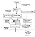
図1は、メモリコントローラ12を含む一実施形態のシステム10を示している。メモリコントローラ12は、複数のマスタ16からバスファブリック18を介してダイナミックランダムアクセスメモリ(DRAM)要求14を受信し、複数のマスタ16の各マスタに割り当てられる優先順位レベルを決定し、DRAMデータバス30上で各マスタにより消費されるDRAMデータバス帯域幅48の量を決定し、各マスタ16に割り当てられた優先順位レベルと、各マスタ16により消費される帯域幅48の量と、に基づいて、細粒度QoSロジック26を適用して、DRAM要求14のスケジュールを算出し、このスケジュールに基づいて、DRAM要求14をDRAMコマンド42に変換し、DRAMコマンドバス34を介してDRAMコマンド42を少なくとも1つのDRAMデバイス32に送信し、少なくとも1つのDRAMデバイス32からDRAMデータバス30を介して応答を受信する、よう構成されている。マスタ16は、例えば、ビデオゲームコンソールのCPU及びGPUであり得、ビデオゲームコンソールのユーザにより現在プレイされているビデオゲームに関連するデータをDRAMデバイス32から読み込むこと又はDRAMデバイス32に書き込むことを要求している最中であり得る。
FIG. 1 illustrates an
要求14がマスタ16により発行されると、システム10は、バスファブリック18を介して要求を送信するよう構成されている。バスファブリックが、図1において、マスタ16とメモリコントローラ12との間に配置された1つのファブリックとして示されている。しかしながら、バスファブリック18は、マスタ16からの全てのトラフィックパターンに対応するのに必要とされる多数のバスセグメントを含み得る。図3は、バスファブリックが、速度リミッタを含むバスセグメント60及び速度リミッタを含まないバスセグメント62を含む複数のバスセグメントに分割されている第2の実施形態のシステム10を示している。図1に戻ると、バスファブリック18は、QoS優先順位割り当てロジック20を適用して、マスタ16の各マスタに割り当てられた優先順位レベルに基づいて要求14の各要求に優先順位レベルを割り当てるよう構成され得る。優先順位レベルは、システム10上で動作するソフトウェアアプリケーションにより、マスタ16の各マスタに割り当てられ得る。そのような割り当ては、例えば、システム10の起動のたびに1回、アプリケーションがシステム10上で実行されるときのアプリケーション境界上で、又は、システム10上の仮想環境の各起動時に、生じ得る。マスタ16は、帯域幅変動に敏感であり得るリアルタイムマスタデバイスであって、帯域幅変動が過度になった場合にユーザ体験の低下を生じさせ得るリアルタイムマスタデバイスを含み得る。そのようなリアルタイムマスタデバイスには、システム10上で動作するソフトウェアアプリケーションにより、より高い優先順位レベルが割り当てられ得る。
When the request 14 is issued by the
要求14の各要求に優先順位レベルを割り当てた後、バスファブリック18は、要求をメモリコントローラ12に送信するよう構成され得る。メモリコントローラ12は、さらに、この優先順位レベルに基づいて、複数の優先順位キュー22のうちの1つの優先順位キューに各DRAM要求14を割り当て、複数の優先順位キュー22の各優先順位キュー内のDRAM要求14をスケジューリングするよう構成され得る。
After assigning a priority level to each request in request 14,
要求14をスケジューリングするために優先順位キュー22により使用され得るスケジューリングパラメータを理解するために、DRAMデバイス32の構造及び動作の説明に一時的に移ることが助けになる。DRAMデバイス32は、「ページ」のアレイとして構成され得る。ここで、各ページは、複数のメモリセル(例えば、1ページ当たり8キロビットと16キロビットとの間)を含む。ページは、行及び列状に配置され、さらに、バンクにグループ化され得る。ここで、各バンクは、数万のページを含む。DRAMデバイス32内のページは、要求14のうちの1つの要求によりアクセスされたか否かに応じて、オープン状態であるか又はクローズ状態であるかのいずれかであり得る。システム10は、システム10が起動されたときにはDRAMデバイス32の全てのバンク内の全てのページがクローズ状態であるように、構成され得る。DRAM要求14のうちDRAMデバイス32のバンク内のクローズ状態のページへのアクセスを要求する1つのDRAM要求が発行されたとき、このDRAM要求14は、最初に「ページミス(page miss)」をもたらすことになり、メモリコントローラ12は、「ページオープン操作」を実行して、ターゲットとされたページをオープンする必要がある。ページオープン操作が生じている間、メモリコントローラ12は、そのバンク内のいかなる他のページのコンテンツにもアクセスすることができない。なぜならば、メモリコントローラ12は、通常、どの時点においても各バンク内に1つのオープン状態のページしか許容しないよう構成されているからである。結果として、ページオープン操作中、メモリコントローラ12は、他のバンク内のページをターゲットとする要求14を探すよう構成され得る。
To understand the scheduling parameters that can be used by the
ページがオープン状態であるとき、その同じページにアクセスすることを要求する後続の要求14は、最初にメモリコントローラ12内の「ページヒット(page hit)」をもたらすことになり、したがって、ページオープン操作が実行されることなく完了し得る。したがって、メモリコントローラ12は、「同一ページ収集(same page gathering)」を実行するよう構成され得る。「同一ページ収集」において、同じページへのアクセスを要求する要求14は、ページオープン操作の必要性を低減させるために、一緒にグループ化される。
When a page is open, subsequent requests 14 requesting access to that same page will initially result in a “page hit” in the
後続の要求が、最後に発行された要求と同じバンク内の異なるページをターゲットとした(すなわち、最後の要求が、現在の要求の前に完了した)場合、いわゆる「ページ競合」が発生し、メモリコントローラ12は、要求14によりターゲットとされたページを、ページオープン操作によってオープンする前に、現在オープン状態のページを、「ページクローズ操作」によってクローズしなければならない。ページオープン操作及びページクローズ操作の両方が、DRAMデータバス30上の帯域幅を消費する。DRAMデータバス30上の帯域幅消費が、所与の要求14を完了するのに必要とされるバスサイクルの数として測定され得る。バスサイクルの数、したがって、1回の操作当たりのDRAMデータバス30上で消費される帯域幅48の量が、DRAMデバイス32用に使用される特定のタイプのメモリのタイミングパラメータにより決定される。しかしながら、使用されるメモリのタイプにかかわらず、DRAMデータバス30上の帯域幅消費48は、要求14がページヒットを有するかページミスを有するか又はページ競合を有するかに応じて変わる。
If a subsequent request targets a different page in the same bank as the last issued request (ie, the last request was completed before the current request), a so-called “page conflict” occurs, Before the
さらに、DRAM要求14は、読み取り要求又は書き込み要求のいずれかであり得る。要求14が読み取り要求である場合、メモリコントローラ12は、DRAMコマンドバス34上で「読み取りコマンド」を送信して、予め定められた数のクロックサイクルの後にDRAMデータバス30上で「読み取りデータ」を受信する「読み取り操作」を実行するよう構成されている。要求14が書き込み要求である場合、メモリコントローラ12は、DRAMコマンドバス34上で書き込みコマンドを送信して、予め定められた数のクロックサイクルだけ待機した後にDRAMデータバス30上で書き込みデータを送信する書き込み操作を実行するよう構成されている。しかしながら、要求14が書き込み要求であり、最後に発行された要求が読み取り要求であった場合、メモリコントローラ12は、データバス30の使用における競合から生じるデータハザード(すなわち、データの処理を誤るリスク)を回避するために、「読み取りから書き込みへのバスターンアラウンド(リードツーライトバスターンアラウンド:read to write bus turnaround)」を実行するよう構成されている。例えば、書き込み操作が開始されたときに、読み取りデータがDRAMデータバス30上でまだ返ってきている場合、送信する書き込みデータと受信する読み取りデータとの間のバス衝突が発生し得る。書き込み操作中におけるそのような発生を回避するために、書き込み操作を開始する前に、メモリコントローラ12は、前の読み取りデータがDRAMデータバス30上で返されていないことを確認するよう構成され得る。競合が存在するときには、メモリコントローラ12は、「読み取りから書き込みへのバスターンアラウンド」を実行するよう構成され得る。「読み取りから書き込みへのバスターンアラウンド」において、書き込みデータをDRAMデバイス32に送信する前にデータバス30上で読み取りデータが返されることを可能にするために、書き込みコマンドが遅延される。同様に、要求14が読み取り要求であり、最後に発行された要求が書き込み要求であった場合、メモリコントローラ12は、読み取りデータがDRAMデバイス32からDRAMデータバス30を介してメモリコントローラ12に返される前に書き込みデータがDRAMデバイス32のメモリに書き込まれることを可能にするために、読み取りコマンドを遅延させる「書き込みから読み取りへのバスターンアラウンド(ライトツーリードバスターンアラウンド:write to read bus turnaround)」を実行するよう構成されている。「読み取りから書き込みへのバスターンアラウンド」操作及び「書き込みから読み取りへのバスターンアラウンド」操作の両方は、複数のバスサイクル、したがって、DRAMデータバス30上の帯域幅量を消費する。したがって、要求14を完了するのに必要とされるDRAMデータバス30上で消費される帯域幅48の量は、メモリコントローラ12によりDRAMデバイス32に発行されている現在の要求14の要求タイプ(すなわち、読み取り又は書き込み)と、最後に発行された要求14の要求タイプと、の両方に依存し得る。この帯域幅消費を最小にするために、メモリコントローラ12は、「読み取り/書き込みグループ化」を実行するよう構成され得る。「読み取り/書き込みグループ化」において、要求14は、「読み取りから書き込みへのバスターンアラウンド」操作及び「書き込みから読み取りへのバスターンアラウンド」操作の必要性を低減させるために、要求タイプに基づいてグループ化される。
Further, the DRAM request 14 can be either a read request or a write request. If the request 14 is a read request, the
さらに、要求14が読み取り要求である場合、この要求14を発行するマスタ16は、DRAMデバイス32にまだ書き込まれていないデータを要求している最中であり得る。データが書き込まれる前にこの要求14を発行するのを回避するために、要求14のページアドレスが、全ての優先順位キュー22内の全ての書き込み要求14のページアドレスと比較されなければならない。このプロセスは、アドレス競合解決(address conflict resolution)と呼ばれ、データ整合性を確実にするために使用され得る。合致がある場合、当該の読み取り要求14は、全ての前の書き込み要求14が完了するまで待機しなければならない。
Further, if request 14 is a read request,
以下に示す表1は、要求されたページの位置、要求タイプ、及び、所与の要求14が生成された時点におけるDRAMデバイス32の状態(すなわち、前に完了した要求タイプ)に基づく、所与の要求14のいくつかの一般的なケースの帯域幅コストの例を示している。

上記表1において、変数BLは、DRAMデバイス32のバースト長を示す。BL/2は、DDRn、低電力DDRn(LPDDRn)、又はグラフィックスDDRn(GDDRn)等の任意のダブルデータレートメモリデバイスについてDRAMデバイス32から読み取られるデータ又はDRAMデバイス32に書き込まれるデータを搬送するDRAMデータバス30がビジーとなる継続時間である。変数tACTは、ページをオープンする帯域幅コストであり、上述したようにページをアクティブ化するのに要する時間である。tPREは、ページをクローズする帯域幅コストであり、上述したようにオープン状態のページをクローズするのに要する時間である。tW2Rは、上述したように書き込みから読み取りへのバスターンアラウンド操作を実行することにより、書き込み操作に続く読み取り操作のためにDRAMデータバス30を遷移させるのに必要とされる、DRAMデータバス30のサイクルの数として表されるコストである。tR2Wは、上述したように読み取りから書き込みへのバスターンアラウンド操作を実行することにより、読み取り操作に続く書き込み操作のためにDRAMデータバス30を遷移させるのに必要とされる、DRAMデータバス30のサイクルの数として表されるコストである。重要なことは、異なるDRAMメモリデバイス(例えば、DDR3、LPDDR3、又はGDDR3)は、これらのパラメータについて異なる名前を使用することがあるが、本開示で説明するコンセプトは、上記DRAMデバイスのいずれにも適用されることに留意することである。以下の段落において詳細に説明するリフレッシュ操作は、表1には含まれていないことに留意されたい。なぜならば、リフレッシュ操作は、マスタ16のオーバーヘッドコストではなく、DRAMデバイス32のオーバーヘッドコストと考えられるからである。
In Table 1 above, the variable BL indicates the burst length of the DRAM device 32. BL / 2 is a DRAM that carries data read from or written to DRAM device 32 for any double data rate memory device such as DDRn, low power DDRn (LPDDRn), or graphics DDRn (GDDRn) This is the duration for which the
表1は、システム10の1つの可能な実施形態を表している。システム10は、表1に列挙されるパラメータに限定されるものではなく、QoSスキームの最終目的に応じて、他の表が、所望の結果を達成するために本明細書で説明する原理に従って構成され得る。
Table 1 represents one possible embodiment of the
メモリコントローラ12は、DRAMデータバス30上の帯域幅消費を最小にするために、上記方法に従って、優先順位キュー22内のDRAM要求14をスケジューリングするよう構成され得る。各優先順位キュー22は、複数のキュー46を含み得る。各優先順位レベルについての優先順位キュー22の数及びサイズ、並びに、優先順位キュー22の各優先順位キュー内のキュー46の数は、実装に応じて変わり得る。図1においては、N個のマスタデバイス16及びM個の優先順位キュー22が示されている。所与の優先順位レベルについての優先順位キュー22の各優先順位キュー内のキュー46は、少なくとも1つの読み取りキューと1つの書き込みキューとを含み得る。メモリコントローラ12は、複数の優先順位キュー22の各優先順位キュー内の要求14をスケジューリングするよう構成され得る。スケジュールは、マスタ依存であり、アドレス競合解決、同一ページ収集、読み取り/書き込みグループ化、及び、要求14の各要求に割り当てられた優先順位レベル等のパラメータに基づき得る。
The
メモリコントローラ12は、さらに、DRAM要求14をマスタスケジューリングマルチプレクサ24に送信し、各マスタ16に割り当てられた帯域幅の未使用部分を定期的にモニタリングし、帯域幅の未使用部分が予め定められたレベル以下に低下した場合にメモリコントローラ12におけるDRAM要求14を調整する(throttle)よう構成され得る。メモリコントローラ12は、上述したスケジューリングパラメータに基づいて、優先順位キュー22から最良の要求14の候補を選択した後、DRAM要求14をマスタスケジューリングマルチプレクサ24に送信するよう構成され得る。
The
マスタスケジューリングマルチプレクサ24は、DRAMデータバス30における予め定められた量の帯域幅を、複数のマスタ16の各マスタに割り当てるよう構成されている細粒度QoS帯域幅プロビジョニングロジック28を含む細粒度QoSロジック26を適用するよう構成され得る。細粒度QoSロジック26は、DRAMデバイス32の帯域幅を、有効(useful)QoS帯域幅及びオーバーヘッド帯域幅という2つのカテゴリに分割するよう構成され得る。オーバーヘッド帯域幅は、DRAMデバイス32の適切な動作を確実にするためにメモリコントローラ12により消費される帯域幅であり得、リフレッシュ操作について消費される帯域幅を含み得る。リフレッシュ操作中、メモリコントローラ12は、DRAMデバイス32の全てのバンクへの全ての読み取り操作及び書き込み操作を中断し、全てのオープン状態のページをクローズし、DRAMデバイス32内の全てのページのコンテンツをリフレッシュするためにリフレッシュコマンドを発行するよう構成されている。リフレッシュ操作が完了した後、メモリコントローラ12は、読み取り操作及び書き込み操作を再開するよう構成されている。有効QoS帯域幅は、DRAMデバイス32に対して読み取り操作及び書き込み操作等の操作を実行するためにマスタ16により消費される帯域幅48を含み得る。メモリコントローラ12は、細粒度QoS帯域幅プロビジョニングロジック28により、予め定められた量の有効QoS帯域幅をマスタ16に割り当てるよう構成され得る。マスタ16の各マスタに割り当てられる帯域幅の量は、システム10上で動作するソフトウェアアプリケーションにより決定され得る。そのような割り当ては、例えば、システム10の起動のたびに1回、アプリケーションがシステム10上で実行されるときのアプリケーション境界上で、又は、システム10上の仮想環境の各起動時に、生じ得る。
The master scheduling multiplexer 24 includes a fine-
メモリコントローラ12は、各要求14についてDRAMデータバス30上で各マスタ16により消費される帯域幅48を算出し、細粒度QoS帯域幅プロビジョニングロジック28により各マスタ16に割り当てられた有効QoS帯域幅の量から、算出された帯域幅48を減算することにより、各マスタ16についての帯域幅の未使用部分を決定するよう構成され得る。メモリコントローラ12は、要求14を完了するのに必要とされる、DRAMデータバス30のバスサイクルの数の観点で、要求14により消費される帯域幅48を測定するよう構成され得る。要求14を完了するのに必要とされるバスサイクルの数は、要求タイプ(すなわち、読み取り又は書き込み)、DRAMデバイス32内の、要求14によりターゲットとされたページが、現在オープン状態であるか又はクローズ状態であるか、及び、要求14によりターゲットとされたページが、最後に発行された要求によりターゲットとされたページと同じバンク内に位置するか否か等の、要求14の様々な特性に応じて変わり得る。
The
メモリコントローラ12の細粒度QoSロジック26は、さらに、QoSクレジットアキュムレータ(QoS credit accumulator)36を含むよう構成され得る。QoSクレジットアキュムレータ36は、複数のマスタ16の各マスタについてのクレジットをインクリメンタルに累積するよう構成され得る。累積のレートは、細粒度QoS帯域幅プロビジョニングロジック28により各マスタに割り当てられた帯域幅に対応し得、各マスタ16についての総クレジットは、予め定められた最大QoSクレジット値を超えることができない。例えば、DRAMデータバス30における毎秒1ギガビットの帯域幅が、所与のマスタ16に割り当てられ、DRAMデータバス30が、200MHz(毎秒200000000サイクル)のクロック周波数で動作している場合、QoSクレジットアキュムレータ36は、当該のマスタ16について指定される、1サイクル当たり5バイトに値するクレジットを累積する。マスタ16が、要求14を発行する場合、要求14により消費される帯域幅48は、QoSクレジットアキュムレータ36における、このマスタ16に対応するクレジットから減算される。マスタ16が、要求14を発行しない場合、QoSクレジットアキュムレータ36は、このマスタ16についての総クレジットが最大QoSクレジット値に達するまで、1サイクル当たり5バイトのレートでクレジットを累積し続ける。システム10は、システム10上で動作するソフトウェアアプリケーションが最大QoSクレジット値を決定することを可能にするよう構成され得る。
The fine
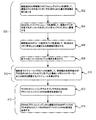
細粒度QoSロジック26は、DRAMデータバス上で各DRAMメモリ要求により消費される帯域幅48を算出し、QoSクレジットアキュムレータにおける、各マスタに対応するクレジットから、算出された帯域幅を減算することにより、各マスタについてのクレジット残余(credit balance)を算出するよう構成され得る細粒度QoSチャージ勘定ロジック(fine-grained QoS charge accounting logic)38をさらに含むよう構成され得る。図2は、細粒度QoSチャージ勘定ロジック38の動作に含まれ得るプロセスの概略図を示している。図示されるように、細粒度QoSチャージ勘定ロジック38は、優先順位キュー22から、現在キューされている要求に関する、現在の要求の情報50を受信するよう構成され得る。現在の要求の情報50は、優先順位キュー22からマスタスケジューリングマルチプレクサ24に現在送信されている要求14によりターゲットとされたページのページアドレス及びバンク、並びに要求14の要求タイプ(すなわち、読み取り又は書き込み)を含み得る。加えて、細粒度QoSチャージ勘定ロジック38は、さらに、DRAMプロトコルエンジン44から、最後に発行された要求の情報52を受信するよう構成され得る。最後に発行された要求の情報52は、DRAMデバイス32に最後に送信された要求14によりターゲットとされたページのページアドレス及びバンク、並びに要求14の要求タイプ(すなわち、読み取り又は書き込み)を含み得る。最後に発行された要求の情報52は、DRAMデバイス32に最後に発行された要求14が、ページヒットを有していたかページミスを有していたか又はページ競合を有していたかをさらに含み得る。細粒度QoSチャージ勘定ロジック38は、さらに、現在の要求の情報50及び最後に発行された要求の情報52の一方又は両方を使用して、要求14によりDRAMデータバス30上で消費される帯域幅48を算出し、QoSクレジットアキュムレータ36における、この要求14を発行したマスタに対応するクレジットから、算出された帯域幅の量を減算するよう構成され得る。細粒度QoSチャージ勘定ロジック38はまた、DRAMプロトコルエンジン44から受信されたグローバルページステータス情報58を使用するよう構成され得る。グローバルページステータス情報58は、DRAMデバイス32内の全てのページの現在のステータスを含み得る。細粒度QoSチャージ勘定ロジック38は、グローバルページステータス情報58を使用して、DRAMデバイス32に発行されるならば、どの要求14が、ページヒット、ページミス、又はページ競合を有することになるかを判定することができる。細粒度QoSチャージ勘定ロジック38は、さらに、QoSクレジットアキュムレータ36における総クレジットから、要求14により消費される帯域幅48を減算する前に、リフレッシュにより消費されるグローバルなオーバーヘッド帯域幅56と、リフレッシュについての1クロックサイクル当たりのクレジットゲイン(credit gain)54と、を考慮に入れるよう構成され得る。システム10は、有効QoS帯域幅のみをマスタ16に割り当てるよう構成され得るので、細粒度QoSチャージ勘定ロジック38は、リフレッシュ操作により消費される帯域幅又は他の形態のオーバーヘッド帯域幅消費を補償するために、1クロックサイクル当たりのクレジットゲインを提供するよう構成され得る。QoSチャージ勘定ロジック38が、最後に発行された要求14により消費された帯域幅48を減算した後、細粒度QoSクレジットアキュムレータ36は、さらに、マスタ16の各マスタについての、QoSクレジットアキュムレータ36における現在の残余を、以下で説明するQoSスケジューリングロジック40に送信するよう構成され得る。
Fine
図1に戻ると、細粒度QoSロジック26は、さらに、各DRAM要求の優先順位クラスに基づいてDRAM要求14をスケジューリングし、DRAM要求14を発行したマスタ16についての、QoSクレジットアキュムレータ36におけるクレジット残余が、予め定められた最小QoSクレジット値未満である場合に、DRAM要求14を調整するよう構成されている細粒度QoSスケジューリングロジック40を含むよう構成され得る。細粒度QoSスケジューリングロジック40は、細粒度QoSチャージ勘定ロジック38から、キューされている要求14の各要求に対応する、マスタ16の各マスタについての現在のクレジット残余を受信するよう構成され得る。細粒度QoSスケジューリングロジック40は、さらに、最高優先順位レベルと、予め定められた最小QoSクレジット値以上のクレジット残余と、を有する要求14を選択するよう構成され得る。要求14が、最小QoSクレジット値未満のクレジット残余を有する場合、細粒度QoSスケジューリングロジック40は、その要求14の優先順位レベルにかかわらず、その要求14を調整するよう構成され得る。複数の要求14が、同じ優先順位レベルと、最小QoSクレジット値以上のクレジット残余と、を有する場合、スケジューリングは、ラウンドロビン方式で、又は、別の適切なデフォルトスケジューリングアルゴリズムに従って、実行され得る。全ての利用可能な要求14が、最小QoSクレジット値未満のクレジット残余を有する場合、最高優先順位レベルを有する要求14が選択され得る。システム10は、システム10上で動作するソフトウェアアプリケーションが最小QoSクレジット値を決定することを可能にするよう構成され得る。
Returning to FIG. 1, the fine-
メモリコントローラ12は、さらに、マスタスケジューリングマルチプレクサ24からDRAM要求14を受信し、DRAMコマンドバス34を介してDRAM要求14をDRAMデバイス32に送信するよう構成されているDRAMプロトコルエンジン44を含むよう構成され得る。DRAMプロトコルエンジン44は、細粒度QoSロジック26により作成されたスケジュールに基づいて、マスタスケジューリングマルチプレクサ24により選択されたDRAM要求14を受信するよう構成され得る。メモリコントローラ12は、さらに、DRAM要求14をDRAMプロトコルエンジン44に送信する前に、DRAM要求14をDRAMコマンド42に変換するよう構成され得る。DRAMプロトコルエンジン44は、さらに、DRAMデバイス32から応答を受信し、最後に発行された要求14に関する情報を細粒度QoSチャージ勘定ロジック38に送信するよう構成され得る。任意的に、DRAMプロトコルエンジン44は、DRAM要求14が成功裡に完了したことをメモリコントローラ12に通知するための割り込みの形態であり得る応答を、DRAMデバイス32から受信するよう構成されてもよい。DRAMプロトコルエンジン44は、さらに、図2に示され説明した最後に発行された要求の情報52を細粒度QoSチャージ勘定ロジック38に送信するよう構成され得る。この情報は、要求14の要求タイプ(すなわち、読み取り又は書き込み)、要求14によりターゲットとされたページのページアドレス及びバンク、並びに、要求14がページヒットを有していたかページミスを有していたか又はページ競合を有していたかを含み得る。
The
図3は、細粒度QoSロジックを実行して、DRAMデータバスの帯域幅をプロビジョニングするよう構成されている第2の実施形態のシステム100を示している。システム100は、システムオンチップ(SoC)101を含み、マスタ16、バスファブリック18、及びDRAMメモリコントローラ12が、SoC101上に形成されており、DRAMメモリコントローラ12が、DRAMデバイス32と通信する。DRAMデバイス32は、SoC101上に形成されることもあるし、独立したデバイスとして形成されることもある。システムオンチップ上に形成されている様々なコンポーネントは、上述したものと同様に機能し、簡潔さのために再度説明しない。上述したように、この実施形態においては、バスファブリックは、速度リミッタを含むバスセグメント60及び速度リミッタを含まないバスセグメント62を含む複数のバスセグメントに分割されている。システムオンチップ101は、バスファブリック上の最少固定量の帯域幅が各マスタのために予約されることを確実にしつつ、各マスタにより消費される最大帯域幅を制限することにより、各マスタがこの固定量を超えないことを確実にするために、速度リミッタを利用することが理解されよう。これは、スケジューリング競合を回避させ、速度制限されたマスタからDRAMデバイスへの効率的なアクセスを促進させる。バスファブリックのうち速度制限されていないバスセグメント(例えば、バスセグメントM)のみを経由する新たなマスタが、このようなシステムに追加される場合、このマスタは、バスファブリック上の過度の帯域幅を消費し得る、且つ/又は、固定量の予約された帯域幅を有するという予測の下で設計された他のマスタの性能を劣化させ得る。したがって、速度リミッタは、何らかのスケジューリング制御を実施するが、バスセグメントM上には速度リミッタが構成されないので、特に速度制限されていないバスセグメントMを通過するDRAM要求は、スケジューリングマルチプレクサ24により適用される細粒度QoSスケジューリング及び優先順位レベルから恩恵を受けることができ、これは、バスセグメントMを介して接続されるマスタによる予約された帯域幅の想定外の消費を防止する。これは、全てのマスタの性能を向上させることができる。
FIG. 3 illustrates a second embodiment of the
次に図4に移ると、メモリコントローラにおいて細粒度帯域幅プロビジョニングを実行するための方法400のフローチャートが示されている。以下に記載の方法は、図1及び図2を参照して上述したシステム10のハードウェア上で実行されてもよいし、他の適切なハードウェア上で実行されてもよい。本明細書に記載の方法が実行され得る適切なハードウェアは、ラップトップパーソナルコンピュータ、デスクトップパーソナルコンピュータ、スマートフォン、ビデオゲームコンソール、タブレットコンピューティングデバイス、スマートテレビジョン等を含むことが理解されよう。本方法のいくつかの実装においては、図4における破線内のステップは省かれてもよいが、他の実装においては、破線内のステップが含まれる。
Turning now to FIG. 4, a flowchart of a
方法400は、402において、複数のマスタからバスファブリックを介してダイナミックランダムアクセスメモリ(DRAM)要求を受信することを含み得る。404において、方法400は、DRAM要求の各DRAM要求に割り当てられる優先順位レベルを決定することを含み得る。
The
502において、方法400は、この優先順位レベルに基づいて、複数の優先順位キューのうちの1つの優先順位キューに各DRAM要求を割り当てることを含み得る。
At 502, the
506において、方法400は、DRAM要求をマスタスケジューリングマルチプレクサに送信することを含み得る。
At 506,
406において、方法400は、DRAMデータバス上で各マスタにより消費されるDRAMデータバス帯域幅の量を決定することを含み得る。508において、これは、各マスタに割り当てられた帯域幅の未使用部分を定期的にモニタリングすることにより少なくとも部分的に達成され得ることが示されている。
At 406, the
408において、方法400は、各マスタに割り当てられた優先順位クラスと、各マスタにより消費されるDRAMデータバス帯域幅の量と、に基づいて、細粒度サービス品質(QoS)ロジックを適用して、DRAM要求のスケジュールを算出することを含み得る。510において、このスケジュールは、帯域幅の未使用部分が予め定められたレベル以下に低下した場合にメモリコントローラにおけるDRAM要求を調整するように算出され得ることが示されている。
At 408, the
410において、方法400は、ステップ408において作成されたスケジュールに基づいて、DRAM要求をDRAMコマンドに変換することを含み得る。412において、方法400は、DRAMコマンドバスを介してDRAMコマンドを少なくとも1つのDRAMデバイスに送信することを含み得る。414において、方法400は、少なくとも1つのDRAMデバイスからDRAMデータバスを介して応答を受信することを含み得る。
At 410, the
図5は、図4の方法400のステップ508、ステップ510、及びステップ412を達成することができる例示的なサブステップを例示しているフローチャートを示している。方法400のステップ508は、サブステップ602〜608を実行することにより達成され得る。602において、方法は、細粒度QoS帯域幅プロビジョニングロジックを適用して、複数のマスタの各マスタに、DRAMデータバスにおける予め定められた量の帯域幅を割り当てることを含み得る。604において、方法は、QoSクレジットアキュムレータを適用して、複数のマスタの各マスタについてのクレジットをインクリメンタルに累積することを含み得る。ここで、累積のレートは、細粒度QoS帯域幅プロビジョニングロジックにより各マスタに割り当てられた帯域幅に対応し、各マスタについての総クレジットは、予め定められた最大QoSクレジット値を超えない。606において、方法は、細粒度QoSチャージ勘定ロジックを適用して、各DRAMメモリ要求により消費されるDRAMデータバス上の帯域幅を算出することを含み得る。608において、方法は、QoSクレジットアキュムレータにおける、各マスタに対応するクレジットから、算出された帯域幅48を減算することにより、各マスタについてのクレジット残余を算出することを含み得る。
FIG. 5 shows a flowchart illustrating exemplary sub-steps that can accomplish
方法400のステップ510は、サブステップ610により達成され得る。サブステップ610に示されるように、細粒度スケジューリングロジックを適用すること、及び、帯域幅の未使用部分が予め定められたレベル以下に低下した場合にメモリコントローラにおけるDRAM要求を調整することは、細粒度QoSスケジューリングロジックを適用して、各要求の優先順位クラスに基づいてDRAM要求をスケジューリングし、DRAM要求を発行したマスタについての、QoSクレジットアキュムレータにおけるクレジット残余が、予め定められた最小QoSクレジット値未満である場合にDRAM要求を調整するようにスケジュールを算出することにより、達成される。
Step 510 of
方法400のステップ412は、サブステップ612〜614により達成され得る。612において、方法は、マスタスケジューリングマルチプレクサからDRAMプロトコルエンジンにDRAM要求を送信することを含み得る。614において、方法は、DRAMプロトコルエンジンから複数のDRAMデバイスのうちの少なくとも1つのDRAMデバイスにDRAM要求を送信することを含み得る。
Step 412 of
図6は、図4の方法400のステップ406を達成することができる例示的なサブステップ650、652を例示しているフローチャートを示している。650において、方法は、DRAMプロトコルエンジンから、最後に発行された要求に関する情報を受信することを含み得る。652において、方法は、最後に発行された要求に関する情報に基づいて、各DRAMメモリ要求により消費されるDRAMデータバス上の帯域幅を算出することを含み得る。
FIG. 6 shows a flow chart illustrating
一時的に図1に戻ると、システム10は、システム10よりも少ない総メモリ帯域幅を有する異なるシステム上で動作するよう元々設計された1以上のソフトウェアプログラムの性能をモデル化するためにも使用され得る。そうするために、マスタ16からの要求14の一部が、こうしたソフトウェアプログラムの実行から生じたものとしてタグ付けされ得る。メモリコントローラ12は、こうしたソフトウェアプログラムが、元々設計された対象のシステム上で動作しているならばマスタ16が受けたであろう帯域幅及びQoSを算出することができる。次いで、メモリコントローラ12は、この算出を用いて、帯域幅及びQoSを、システム10上の要求14に割り当てることができる。したがって、コンピューティングデバイスは、さらに、複数のマスタからのメモリ要求の一部を、このコンピューティングデバイスよりも少ない総メモリ帯域幅を有するシステム上で動作するよう元々設計された1以上のソフトウェアプログラムの実行から生じたものとしてタグ付けし、1以上のソフトウェアプログラムが、より少ない総メモリ帯域幅を有する上記システム上で動作しているならば複数のマスタが受けたであろう帯域幅及びQoSを算出するよう構成され得る。さらに、コンピューティングデバイスは、これら帯域幅及びQoSを、複数のマスタからのメモリ要求に割り当て、結果として、より少ない総メモリ帯域幅を有する上記システム上での1以上のソフトウェアプログラムの性能をモデル化するよう構成され得る。
Returning temporarily to FIG. 1,
上述したシステム及び方法は、種々の有用な産業上の用途を有する。例えば、第1の用途は、より高速なメモリタイプが、より低速なメモリタイプと同じ帯域幅変動をもたらすことを可能にすることである。例えば、システムは、例えば、2133Mbpsのクロック周波数で動作するダブルデータレート3(DDR3)メモリを使用するよう設計されたビデオゲームコンソールであり得る。ビデオゲームコンソールのライフサイクル中に、このメモリを、例えば、2400Mbpsのクロック周波数で動作するダブルデータレート4(DDR4)メモリに変更することが、(例えば、性能又はコスト上の理由で)有利なことがある。ビデオゲームコンソールのライフサイクル中にそのような変更がなされると、DDR3とともに使用されるよう設計されたソフトウェアが、DDR4とともには適切に動作しないリスクが存在するようになる。しかしながら、上述した細粒度QoSロジックは、DDR4に対するプロビジョニングが、DDR3に対するプロビジョニングと同じであるように、DRAMデータバス上の帯域幅の量が各マスタデバイスにプロビジョニングされることを可能にし得る。したがって、細粒度QoSロジックは、DDR4等の新たな世代のメモリデバイスの帯域幅変動が、DDR3等の前の世代のメモリデバイスと実質的に同様であるように、新たな世代のメモリデバイスを制限し、そうする際、さらなる帯域幅変動を受けることなく、前の世代のメモリデバイス用に設計されたソフトウェアが、後の世代のメモリデバイスを使用するシステム上で機能することを可能にし得る。 The systems and methods described above have a variety of useful industrial applications. For example, a first application is to allow faster memory types to provide the same bandwidth variation as slower memory types. For example, the system may be a video game console designed to use, for example, a double data rate 3 (DDR3) memory operating at a clock frequency of 2133 Mbps. It would be advantageous (eg for performance or cost reasons) to change this memory to a double data rate 4 (DDR4) memory operating at a clock frequency of 2400 Mbps, for example, during the life cycle of a video game console There is. When such changes are made during the life cycle of a video game console, there is a risk that software designed for use with DDR3 will not work properly with DDR4. However, the fine-grained QoS logic described above may allow the amount of bandwidth on the DRAM data bus to be provisioned to each master device so that provisioning for DDR4 is the same as provisioning for DDR3. Therefore, fine-grained QoS logic limits the new generation memory device so that the bandwidth variation of the new generation memory device such as DDR4 is substantially the same as the previous generation memory device such as DDR3. However, in doing so, it may allow software designed for previous generation memory devices to function on systems that use later generation memory devices without experiencing additional bandwidth variations.
上述したシステム及び方法の別の例示的なユースケースシナリオは、さらなるマスタデバイスがシステムに追加されたときにマスタデバイスが受ける帯域幅変動の量を低減させることである。システムが、例えば、ビデオゲームコンソールである場合、ビデオゲームコンソールが発売され、ソフトウェアがそのビデオゲームコンソール用に設計された後であっても、さらなるマスタが追加されることがある。さらなるマスタデバイスは、さらなる帯域幅変動を望ましくない形でシステムにもたらすことがある。しかしながら、細粒度QoSロジックを使用して、マスタデバイスを分離させて、上述した細粒度QoSパラメータ及び優先順位クラスに基づいて、論理的な方法で、マスタデバイスから生成された要求をスケジューリングすることができ、それにより、そうでなければ新たなマスタデバイスを追加することにより生じたであろうさらなる帯域幅変動からシステムを保護することができる。これを達成するために、マスタデバイスに、DRAMデータバス上の固定量の帯域幅を割り当てることができ、全てのマスタデバイスをサポートするのに十分な帯域幅がある限り、各マスタに割り当てられた帯域幅は、新たなマスタが追加されたときにも、変更されないままである。これは、さらなるマスタが追加される前と同じようにマスタデバイスが挙動することを確実にするために必要とされるテストの量の著しい低減をもたらす。そのような用途において、細粒度QoSロジックを使用して、システム内のマスタデバイスの各マスタデバイスについて固定量の帯域幅を予約し、優先順位クラス及び細粒度QoS技術を使用して、既存のマスタの固定量の予約された帯域幅と干渉することから、新たなマスタにより消費される帯域幅を制限する。 Another exemplary use case scenario for the systems and methods described above is to reduce the amount of bandwidth variation that a master device experiences when additional master devices are added to the system. If the system is, for example, a video game console, additional masters may be added even after the video game console is released and the software is designed for that video game console. Additional master devices may introduce additional bandwidth variations into the system in an undesirable manner. However, using fine-grained QoS logic to isolate the master device and schedule requests generated from the master device in a logical manner based on the fine-grained QoS parameters and priority classes described above. Yes, thereby protecting the system from further bandwidth fluctuations that would otherwise have been caused by adding a new master device. To accomplish this, a master device can be assigned a fixed amount of bandwidth on the DRAM data bus, and as long as there is enough bandwidth to support all master devices The bandwidth remains unchanged when a new master is added. This results in a significant reduction in the amount of testing required to ensure that the master device behaves as before additional masters are added. In such applications, fine-grained QoS logic is used to reserve a fixed amount of bandwidth for each master device in the master device, and priority classes and fine-grained QoS techniques are used to create existing masters. Limit the bandwidth consumed by the new master because it interferes with a fixed amount of reserved bandwidth.
第3の例は、上述したシステム及び方法を使用して、物理DRAMデバイスを、多くの論理的に独立したDRAMデバイスにパーティショニングすることである。マスタデバイスを、これらの論理的に独立したDRAMデバイスに割り当てることができ、それにより、他のパーティションに割り当てられた他のマスタデバイスにより引き起こされる帯域幅変動から、マスタデバイスを保護することができる。そのようなパーティションが作成されると、他のパーティション上のマスタデバイスを妨げることなく、マスタデバイスを追加及び除去することができる。 A third example is to partition a physical DRAM device into many logically independent DRAM devices using the system and method described above. Master devices can be assigned to these logically independent DRAM devices, thereby protecting the master device from bandwidth variations caused by other master devices assigned to other partitions. Once such a partition is created, master devices can be added and removed without interfering with master devices on other partitions.
DRAMメモリデバイスのコンテキストにおいて上述したシステム及び方法は、スタティックランダムアクセスメモリ(SRAM)、フラッシュメモリ、磁気ディスクメモリ、テープメモリ、並びに、他の種類の揮発性メモリデバイス及び不揮発性メモリデバイスを含む他のタイプのメモリデバイスに適用されてもよいことが理解されよう。したがって、上述したDRAMデータバスは、メモリデータバスとすることができ、上述したDRAMメモリ要求は、メモリ要求とすることができ、上述したDRAMコマンドは、メモリコマンドとすることができ、上述したDRAMコマンドバスは、メモリコマンドバスとすることができる。これらの様々なメモリコンポーネントは、この段落において上記で列挙されたメモリデバイス等の特定のタイプのメモリデバイスとともに動作するよう構成される。 The systems and methods described above in the context of DRAM memory devices include static random access memory (SRAM), flash memory, magnetic disk memory, tape memory, and other types, including other types of volatile and non-volatile memory devices. It will be appreciated that it may be applied to types of memory devices. Therefore, the above-described DRAM data bus can be a memory data bus, the above-mentioned DRAM memory request can be a memory request, the above-described DRAM command can be a memory command, and the above-described DRAM data bus The command bus can be a memory command bus. These various memory components are configured to operate with certain types of memory devices, such as the memory devices listed above in this paragraph.
図7は、上述したシステム及び方法を実装することができるコンピューティング環境を示している。図7に示されるように、コンピューティングシステム700は、プロセッサ720と不揮発性メモリ722と揮発性メモリ724とを有するホストシステム718を含み得るだけでなく、表示サブシステム706、通信サブシステム708、及び入力サブシステム710を含み得、これらは全て、通信バスサブシステム702を介してリンクされる。
FIG. 7 illustrates a computing environment in which the systems and methods described above can be implemented. As shown in FIG. 7, the computing system 700 can include a host system 718 having a processor 720, non-volatile memory 722, and volatile memory 724, as well as a display subsystem 706, a communication subsystem 708, and An input subsystem 710 may be included, all of which are linked via the
システム10は、1以上のパーソナルコンピュータ、サーバコンピュータ、タブレットコンピュータ、ホームエンターテイメントコンピュータ(ケーブルセットトップボックス、デジタルビデオレコーダ、ビデオサーバ等)、ネットワークコンピューティングデバイス、ゲームデバイス(ゲームコンソール等)、モバイルコンピューティングデバイス、モバイル通信デバイス(例えば、スマートフォン)、及び/又は他のコンピューティングデバイスの形態をとることができる。
The
ホストシステム718のプロセッサ720は、不揮発性メモリ722及び揮発性メモリ724の諸部分を使用して命令を実行するよう構成される物理デバイスである。例えば、プロセッサは、1以上のアプリケーション、サービス、プログラム、ルーチン、ライブラリ、オブジェクト、コンポーネント、データ構造、又は他の論理的構造体の一部である命令を実行するよう構成され得る。そのような命令は、タスクを実行するために、データ型を実装するために、1以上のコンポーネントの状態を変換するために、技術的効果を達成するために、又は所望の結果に達するために、実装され得る。 The processor 720 of the host system 718 is a physical device configured to execute instructions using portions of the non-volatile memory 722 and volatile memory 724. For example, a processor may be configured to execute instructions that are part of one or more applications, services, programs, routines, libraries, objects, components, data structures, or other logical structures. Such instructions may be used to perform tasks, implement data types, convert the state of one or more components, achieve technical effects, or reach a desired result. Can be implemented.
不揮発性メモリ722は、プロセッサ720により実行可能な命令を保持するよう構成される1以上の物理デバイスを含む。不揮発性メモリ722は、フラッシュ、EPROM、EEPROM等といった不揮発性メモリを含み得、処理中に有限の期間の間命令を保持し、コンピューティングシステムに電力が供給されていないときでも、命令を保持し続ける。揮発性メモリ724は、上述したDRAMデバイス32等のDRAMや、処理中に有限の期間の間命令を保持するが、通常は、コンピューティングシステムに電力が供給されなくなった後には命令を記憶し続けることはないRAMを含み得る。 Non-volatile memory 722 includes one or more physical devices configured to hold instructions executable by processor 720. Non-volatile memory 722 may include non-volatile memory such as flash, EPROM, EEPROM, etc., holding instructions for a finite period of time during processing and holding instructions even when power is not supplied to the computing system. to continue. Volatile memory 724 holds instructions for a finite period of time during processing, such as DRAM devices 32 described above, but typically continues to store instructions after power is no longer supplied to the computing system. It may include RAM that does not.
プロセッサ720、永続的メモリ722、及び揮発性メモリ724の態様は、1以上のハードウェアロジックコンポーネントに一緒に統合されてもよい。そのようなハードウェアロジックコンポーネントは、例えば、フィールドプログラマブルゲートアレイ(FPGA)、特定用途プログラム向け集積回路/特定用途向け集積回路(PASIC/ASIC)、特定プログラム向け標準品/特定用途向け標準品(PSSP/ASSP)、システムオンチップ(SoC)、及びコンプレックスプログラマブルロジックデバイス(CPLD)を含み得る。 Aspects of the processor 720, persistent memory 722, and volatile memory 724 may be integrated together in one or more hardware logic components. Such hardware logic components include, for example, field programmable gate arrays (FPGAs), application specific integrated circuits / application integrated circuits (PAASIC / ASIC), application specific standards / application standard (PSSP). / ASSP), system on chip (SoC), and complex programmable logic device (CPLD).
表示サブシステム706は、永続的メモリ722又は揮発性メモリ724により保持されているデータの視覚的表現を提示するために使用され得る。この視覚的表現は、グラフィカルユーザインタフェース(GUI)の形態をとることができる。本明細書に記載の方法及びプロセスは、不揮発性メモリ722又は揮発性メモリ724により保持されているデータを変化させ、したがって、不揮発性メモリ722又は揮発性メモリ724の状態を変換させるので、表示サブシステム706の状態も同様に、元となるデータの変化を視覚的に表現するように変換され得る。表示サブシステム706は、実質的に任意のタイプの技術を利用する1以上の表示デバイスを含み得る。そのような表示デバイスは、共有筐体において、プロセッサ720及び/又は不揮発性メモリ722若しくは揮発性メモリ724と結合されてよいし、そのような表示デバイスは、周辺表示デバイスであってもよい。 Display subsystem 706 may be used to present a visual representation of the data held by persistent memory 722 or volatile memory 724. This visual representation can take the form of a graphical user interface (GUI). The methods and processes described herein change the data held by the non-volatile memory 722 or volatile memory 724, and thus change the state of the non-volatile memory 722 or volatile memory 724, so that the display sub- The state of the system 706 can similarly be converted to visually represent changes in the underlying data. Display subsystem 706 may include one or more display devices that utilize substantially any type of technology. Such a display device may be coupled with the processor 720 and / or the non-volatile memory 722 or the volatile memory 724 in a shared housing, and such a display device may be a peripheral display device.
入力サブシステム710は、キーボード、マウス、タッチスクリーン、又はゲームコントローラ等の1以上のユーザ入力デバイスを含んでもよいし、このような1以上のユーザ入力デバイスとインタフェースをとってもよい。いくつかの実施形態において、入力サブシステムは、選択されたナチュラルユーザ入力(NUI)コンポーネントを含んでもよいし、選択されたNUIコンポーネントとインタフェースをとってもよい。そのようなコンポーネントは、統合されることもあるしペリフェラルであることもあり、入力アクションの変換及び/又は処理は、オンボード又はオフボードで扱われ得る。例示的なNUIコンポーネントは、音声認識及び/又は発話認識のためのマイクロフォン;マシンビジョン及び/又はジェスチャ認識のための赤外線カメラ、カラーカメラ、立体視カメラ、及び/又はデプスカメラ;動き検出及び/又は意図認識のためのヘッドトラッカ、アイトラッカ、加速度計、及び/又はジャイロスコープ;及び、脳活動を評価するための電場検知コンポーネントを含み得る。 The input subsystem 710 may include one or more user input devices such as a keyboard, mouse, touch screen, or game controller, and may interface with one or more such user input devices. In some embodiments, the input subsystem may include a selected natural user input (NUI) component or may interface with the selected NUI component. Such components may be integrated or peripherals, and input action conversion and / or processing may be handled onboard or offboard. Exemplary NUI components include: a microphone for speech recognition and / or speech recognition; an infrared camera, a color camera, a stereoscopic camera, and / or a depth camera for machine vision and / or gesture recognition; motion detection and / or A head tracker, eye tracker, accelerometer, and / or gyroscope for intent recognition; and an electric field sensing component for assessing brain activity.
通信サブシステム708は、システム10を1以上の他のコンピューティングデバイスに通信可能に接続するよう構成され得る。通信サブシステム708は、1以上の異なる通信プロトコルに適合する有線通信デバイス及び/又は無線通信デバイスを含み得る。非限定的な例として、通信サブシステム708は、無線電話網、又は、有線ローカルエリアネットワーク、有線ワイドエリアネットワーク、無線ローカルエリアネットワーク、若しくは無線ワイドエリアネットワークを介する通信用に構成され得る。いくつかの実施形態において、通信サブシステムは、コンピューティングシステム700が、インターネット等のネットワークを介して他のデバイスとの間でメッセージを送信及び/又は受信することを可能にし得る。
Communication subsystem 708 may be configured to communicatively connect
多数の変形が可能であるので、本明細書に記載の構成及び/又はアプローチは、本質的に例示であり、そのような特定の実施形態又は例は、限定とみなされるべきではないことが理解されよう。本明細書に記載の特定のルーチン又は方法は、任意の数の処理方策のうちの1以上を表し得る。したがって、図示及び/又は説明した様々な動作は、図示及び/又は説明した順番で実行されることもあるし、他の順番で実行されることもあるし、並列に実行されることもあるし、省かれることもある。同様に、上述したプロセスの順番も、変更されることがある。 Since numerous variations are possible, it is understood that the configurations and / or approaches described herein are exemplary in nature and that such specific embodiments or examples should not be considered limiting. Let's do it. Particular routines or methods described herein may represent one or more of any number of processing strategies. Accordingly, the various operations illustrated and / or described may be performed in the order illustrated and / or described, may be performed in other orders, or may be performed in parallel. , Sometimes omitted. Similarly, the order of the processes described above may change.
本開示の主題は、様々なプロセス、システム、及び構成、並びに、本明細書で開示した他の特徴、機能、動作、及び/又は特性の全ての新規で非自明なコンビネーション及びサブコンビネーションに加えて、それらのありとあらゆる均等なものを含む。 The subject matter of this disclosure is in addition to all new and non-obvious combinations and sub-combinations of various processes, systems, and configurations, and other features, functions, operations, and / or characteristics disclosed herein. , Including any and all equivalents of them.
Claims (10)
複数のマスタからバスファブリックを介してメモリ要求を受信するステップと、
前記メモリ要求の各メモリ要求に割り当てられる優先順位レベルを決定するステップと、
メモリデバイスから受信された、最後に発行された要求に関する情報に基づいて、要求の帯域幅コストを算出するステップと、
メモリデータバス上で各マスタにより消費される、1つの要求当たりのメモリデータバス帯域幅の量を決定するステップと、
各マスタに割り当てられた優先順位クラスと、前記最後に発行された要求に関する前記情報に基づく、各要求の前記帯域幅コストと、各マスタにより消費される、1つの要求当たりのメモリデータバス帯域幅の量と、に基づいて、サービス品質(QoS)ロジックを適用して、前記メモリ要求のスケジュールを算出するステップであって、各マスタにより消費される、1つの要求当たりの前記メモリデータバス帯域幅は、最後に発行された要求に関する情報であって、該最後に発行された要求によりターゲットとされたページのページアドレス及びバンクと、該最後に発行された要求の要求タイプと、該最後に発行された要求が、ページヒットを有していたかページミスを有していたか又はページ競合を有していたかと、を含む情報に基づいて算出される、ステップと、
前記スケジュールに基づいて、
前記メモリ要求をメモリコマンドに変換するステップと、
メモリコマンドバスを介して前記メモリコマンドを少なくとも1つのメモリデバイスに送信するステップと、
前記少なくとも1つのメモリデバイスから前記メモリデータバスを介して応答を受信するステップと、
を含む方法。 A method for performing bandwidth provisioning in a memory controller, comprising:
Receiving memory requests from a plurality of masters via a bus fabric;
Determining a priority level assigned to each memory request of the memory request;
Calculating a bandwidth cost of the request based on information about the last issued request received from the memory device;
Determining the amount of memory data bus bandwidth per request consumed by each master on the memory data bus;
Based on the priority class assigned to each master and the information about the last issued request, the bandwidth cost of each request and the memory data bus bandwidth per request consumed by each master Applying a quality of service (QoS) logic based on the amount of memory and calculating a schedule of the memory requests, wherein the memory data bus bandwidth per request consumed by each master Is information about the last issued request , the page address and bank of the page targeted by the last issued request, the request type of the last issued request, and the last issued been requested, on the basis whether had or page conflict had or page miss had a page hit, the information including the Is calculated, and the step,
Based on the schedule,
Converting the memory request into a memory command;
Transmitting the memory command to at least one memory device via a memory command bus;
Receiving a response from the at least one memory device via the memory data bus;
Including methods.
前記方法は、
前記優先順位レベルに基づいて、複数の優先順位キューのうちの1つの優先順位キューに各DRAM要求を割り当てるステップ
をさらに含む、請求項1記載の方法。 The at least one memory device is a dynamic random access memory (DRAM) device, the memory data bus is a DRAM data bus, the memory request is a DRAM memory request, and the memory command is a DRAM memory command The memory command bus is a DRAM command bus;
The method
The method of claim 1, further comprising: assigning each DRAM request to a priority queue of a plurality of priority queues based on the priority level.
各マスタに割り当てられた帯域幅の未使用部分を定期的にモニタリングするステップと、
前記帯域幅の前記未使用部分が予め定められたレベル以下に低下した場合に前記メモリコントローラにおける前記DRAM要求を限定するように前記スケジュールを算出するステップと、
をさらに含む、請求項2記載の方法。 Sending the DRAM request from the plurality of priority queues to a master scheduling multiplexer;
Periodically monitoring the unused portion of the bandwidth allocated to each master;
Calculating the schedule to limit the DRAM request in the memory controller when the unused portion of the bandwidth drops below a predetermined level;
The method of claim 2 further comprising:
QoS帯域幅プロビジョニングロジックを適用して、前記複数のマスタの各マスタに、前記DRAMデータバスにおける予め定められた量の帯域幅を割り当てるステップ
を含む、請求項3記載の方法。 The step of periodically monitoring the unused portion of the bandwidth allocated to each master comprises:
The method of claim 3, comprising applying QoS bandwidth provisioning logic to assign a predetermined amount of bandwidth in the DRAM data bus to each master of the plurality of masters.
QoSクレジットアキュムレータを適用して、前記複数のマスタの各マスタについてのクレジットをインクリメンタルに累積するステップであって、累積のレートは、前記QoS帯域幅プロビジョニングロジックにより各マスタに割り当てられた前記帯域幅に対応し、各マスタについての総クレジットは、予め定められた最大QoSクレジット値を超えない、ステップ
を含む、請求項4記載の方法。 The step of periodically monitoring the unused portion of the bandwidth allocated to each master comprises:
Applying a QoS credit accumulator to incrementally accumulate credit for each master of the plurality of masters, the rate of accumulation being equal to the bandwidth allocated to each master by the QoS bandwidth provisioning logic; Correspondingly, the total credit for each master does not exceed a predetermined maximum QoS credit value.
QoSチャージ勘定ロジックを適用して、各DRAMメモリ要求により消費される前記DRAMデータバス上の帯域幅を算出するステップと、
前記QoSクレジットアキュムレータにおける、各マスタに対応する前記クレジットから、前記の算出された帯域幅を減算することにより、各マスタについてのクレジット残余を算出するステップと、
を含む、請求項5記載の方法。 The step of periodically monitoring the unused portion of the bandwidth allocated to each master comprises:
Applying QoS charge accounting logic to calculate the bandwidth on the DRAM data bus consumed by each DRAM memory request;
Calculating a credit residue for each master by subtracting the calculated bandwidth from the credit corresponding to each master in the QoS credit accumulator;
The method of claim 5 comprising:
QoSスケジューリングロジックを適用して、各DRAM要求の前記優先順位クラスに基づいて前記DRAM要求をスケジューリングし、DRAM要求を発行したマスタについての、前記QoSクレジットアキュムレータにおける前記クレジット残余が、予め定められた最小QoSクレジット値未満である場合に、前記DRAM要求を限定するように前記スケジュールを算出する
ことにより達成される、請求項7記載の方法。 Applying scheduling logic to limit DRAM requests in the memory controller when the unused portion of the bandwidth falls below a predetermined level,
Applying QoS scheduling logic to schedule the DRAM request based on the priority class of each DRAM request, the credit residue in the QoS credit accumulator for the master that issued the DRAM request is a predetermined minimum The method of claim 7, wherein the method is achieved by calculating the schedule to limit the DRAM request if it is less than a QoS credit value.
前記マスタスケジューリングマルチプレクサからDRAMプロトコルエンジンに前記DRAM要求を送信することと、
前記DRAMプロトコルエンジンから前記複数のDRAMデバイスのうちの少なくとも1つのDRAMデバイスに前記DRAM要求を送信することと、
を含む、請求項8記載の方法。 Sending the DRAM request to at least one DRAM device of a plurality of DRAM devices;
Sending the DRAM request from the master scheduling multiplexer to a DRAM protocol engine;
Sending the DRAM request from the DRAM protocol engine to at least one DRAM device of the plurality of DRAM devices;
The method of claim 8 comprising:
前記複数のマスタの各マスタに割り当てられる優先順位レベルを決定し、
メモリデバイスから受信された、最後に発行された要求に関する情報に基づいて、要求の帯域幅コストを算出し、
メモリデータバス上で各マスタにより消費される、1つの要求当たりのメモリデータバス帯域幅の量を決定し、
各マスタに割り当てられた優先順位クラスと、前記最後に発行された要求に関する前記情報に基づく、各要求の前記帯域幅コストと、各マスタにより消費される、1つの要求当たりのメモリデータバス帯域幅の量と、に基づいて、サービス品質(QoS)ロジックを適用して、前記メモリ要求のスケジュールを算出し、ここで、各マスタにより消費される、1つの要求当たりの前記メモリデータバス帯域幅は、最後に発行された要求に関する情報であって、該最後に発行された要求によりターゲットとされたページのページアドレス及びバンクと、該最後に発行された要求の要求タイプと、該最後に発行された要求が、ページヒットを有していたかページミスを有していたか又はページ競合を有していたかと、を含む情報に基づいて算出され、
前記スケジュールに基づいて、
前記メモリ要求をメモリコマンドに変換し、
メモリコマンドバスを介して前記メモリコマンドを少なくとも1つのメモリデバイスに送信し、
前記少なくとも1つのメモリデバイスから前記メモリデータバスを介して応答を受信する
よう構成されているメモリコントローラ。 Receive memory requests from multiple masters over the bus fabric,
Determining a priority level assigned to each of the plurality of masters;
Calculate the bandwidth cost of the request based on information about the last issued request received from the memory device,
Determine the amount of memory data bus bandwidth per request consumed by each master on the memory data bus;
Based on the priority class assigned to each master, the bandwidth cost of each request based on the information about the last issued request, and the memory data bus bandwidth per request consumed by each master And applying a quality of service (QoS) logic to calculate a schedule of the memory requests, where the memory data bus bandwidth per request consumed by each master is Information about the last issued request , the page address and bank of the page targeted by the last issued request, the request type of the last issued request, and the last issued request is, whether had or page conflict had or page miss had a page hit, is calculated based on information including
Based on the schedule,
Converting the memory request into a memory command;
Sending the memory command to at least one memory device via a memory command bus;
A memory controller configured to receive a response from the at least one memory device via the memory data bus.
Applications Claiming Priority (3)
| Application Number | Priority Date | Filing Date | Title |
|---|---|---|---|
| US14/252,673 US9563369B2 (en) | 2014-04-14 | 2014-04-14 | Fine-grained bandwidth provisioning in a memory controller |
| US14/252,673 | 2014-04-14 | ||
| PCT/US2015/024414 WO2015160541A1 (en) | 2014-04-14 | 2015-04-06 | Fine-grained bandwidth provisioning in a memory controller |
Publications (3)
| Publication Number | Publication Date |
|---|---|
| JP2017511545A JP2017511545A (en) | 2017-04-20 |
| JP2017511545A5 JP2017511545A5 (en) | 2018-04-26 |
| JP6495327B2 true JP6495327B2 (en) | 2019-04-03 |
Family
ID=52875816
Family Applications (1)
| Application Number | Title | Priority Date | Filing Date |
|---|---|---|---|
| JP2016560970A Active JP6495327B2 (en) | 2014-04-14 | 2015-04-06 | Fine-grained bandwidth provisioning in memory controllers |
Country Status (6)
| Country | Link |
|---|---|
| US (1) | US9563369B2 (en) |
| EP (1) | EP3132355B1 (en) |
| JP (1) | JP6495327B2 (en) |
| KR (1) | KR102380670B1 (en) |
| CN (1) | CN106233269B (en) |
| WO (1) | WO2015160541A1 (en) |
Families Citing this family (24)
| Publication number | Priority date | Publication date | Assignee | Title |
|---|---|---|---|---|
| KR101699377B1 (en) * | 2014-07-02 | 2017-01-26 | 삼성전자주식회사 | Storage device including nonvolatile memory and memory controller and operating method of storage device |
| WO2016122662A1 (en) * | 2015-01-30 | 2016-08-04 | Hewlett Packard Enterprise Development Lp | Memory network to prioritize processing of a memory access request |
| US10158712B2 (en) * | 2015-06-04 | 2018-12-18 | Advanced Micro Devices, Inc. | Source-side resource request network admission control |
| US10298511B2 (en) | 2016-08-24 | 2019-05-21 | Apple Inc. | Communication queue management system |
| US10613612B2 (en) | 2017-03-16 | 2020-04-07 | Qualcomm Incorporated | Power reduction via memory efficiency compensation |
| CN109154883A (en) * | 2017-03-22 | 2019-01-04 | 波利伍德有限责任公司 | Driving stage internal service quality |
| US10795836B2 (en) * | 2017-04-17 | 2020-10-06 | Microsoft Technology Licensing, Llc | Data processing performance enhancement for neural networks using a virtualized data iterator |
| US10437482B2 (en) * | 2017-07-25 | 2019-10-08 | Samsung Electronics Co., Ltd. | Coordinated near-far memory controller for process-in-HBM |
| US10481944B2 (en) * | 2017-08-09 | 2019-11-19 | Xilinx, Inc. | Adaptive quality of service control circuit |
| US10360832B2 (en) | 2017-08-14 | 2019-07-23 | Microsoft Technology Licensing, Llc | Post-rendering image transformation using parallel image transformation pipelines |
| US10678690B2 (en) | 2017-08-29 | 2020-06-09 | Qualcomm Incorporated | Providing fine-grained quality of service (QoS) control using interpolation for partitioned resources in processor-based systems |
| US10318301B2 (en) | 2017-08-31 | 2019-06-11 | Micron Technology, Inc. | Managed multiple die memory QoS |
| US10372609B2 (en) * | 2017-09-14 | 2019-08-06 | Intel Corporation | Fast cache warm-up |
| KR102417977B1 (en) * | 2017-10-19 | 2022-07-07 | 에스케이하이닉스 주식회사 | Memory system and operating method thereof |
| US10296230B1 (en) * | 2017-12-22 | 2019-05-21 | Advanced Micro Devices, Inc. | Scheduling memory requests with non-uniform latencies |
| US10275352B1 (en) * | 2017-12-28 | 2019-04-30 | Advanced Micro Devices, Inc. | Supporting responses for memory types with non-uniform latencies on same channel |
| US11144457B2 (en) * | 2018-02-22 | 2021-10-12 | Netspeed Systems, Inc. | Enhanced page locality in network-on-chip (NoC) architectures |
| US10705985B1 (en) * | 2018-03-12 | 2020-07-07 | Amazon Technologies, Inc. | Integrated circuit with rate limiting |
| CN109062514B (en) * | 2018-08-16 | 2021-08-31 | 郑州云海信息技术有限公司 | Bandwidth control method and device based on namespace and storage medium |
| US10838884B1 (en) | 2018-09-12 | 2020-11-17 | Apple Inc. | Memory access quality-of-service reallocation |
| US10635355B1 (en) * | 2018-11-13 | 2020-04-28 | Western Digital Technologies, Inc. | Bandwidth limiting in solid state drives |
| US10860254B2 (en) * | 2019-04-17 | 2020-12-08 | Vmware, Inc. | Throttling resynchronization operations in a data store cluster based on I/O bandwidth limits |
| US20210279192A1 (en) * | 2020-03-06 | 2021-09-09 | Infineon Technologies Ag | Distribution of interconnect bandwidth among master agents |
| WO2023128479A1 (en) * | 2021-12-30 | 2023-07-06 | 주식회사 엘엑스세미콘 | Memory control system and display device including memory control function |
Family Cites Families (14)
| Publication number | Priority date | Publication date | Assignee | Title |
|---|---|---|---|---|
| FR2778258A1 (en) | 1998-04-29 | 1999-11-05 | Texas Instruments France | Memory traffic access controller |
| US6961834B2 (en) | 2001-10-12 | 2005-11-01 | Sonics, Inc. | Method and apparatus for scheduling of requests to dynamic random access memory device |
| US6804738B2 (en) * | 2001-10-12 | 2004-10-12 | Sonics, Inc. | Method and apparatus for scheduling a resource to meet quality-of-service restrictions |
| US7363427B2 (en) * | 2004-01-12 | 2008-04-22 | Hewlett-Packard Development Company, L.P. | Memory controller connection to RAM using buffer interface |
| US7461214B2 (en) | 2005-11-15 | 2008-12-02 | Agere Systems Inc. | Method and system for accessing a single port memory |
| CN101046784A (en) * | 2006-07-18 | 2007-10-03 | 威盛电子股份有限公司 | Memory data access system and method and memory controller |
| US7577780B2 (en) | 2007-02-28 | 2009-08-18 | National Chiao Tung University | Fine-grained bandwidth control arbiter and the method thereof |
| US8452920B1 (en) | 2007-12-31 | 2013-05-28 | Synopsys Inc. | System and method for controlling a dynamic random access memory |
| US8180975B2 (en) | 2008-02-26 | 2012-05-15 | Microsoft Corporation | Controlling interference in shared memory systems using parallelism-aware batch scheduling |
| CN101876944B (en) | 2009-11-26 | 2012-02-15 | 威盛电子股份有限公司 | DRAM (Dynamic Random Access Memory) controller and control method |
| US8898674B2 (en) | 2009-12-23 | 2014-11-25 | International Business Machines Corporation | Memory databus utilization management system and computer program product |
| US8314807B2 (en) | 2010-09-16 | 2012-11-20 | Apple Inc. | Memory controller with QoS-aware scheduling |
| WO2012036905A1 (en) | 2010-09-16 | 2012-03-22 | Apple Inc. | Multi-ported memory controller with ports associated with traffic classes |
| JP2013196321A (en) | 2012-03-19 | 2013-09-30 | Pfu Ltd | Electronic circuit and arbitration method |
-
2014
- 2014-04-14 US US14/252,673 patent/US9563369B2/en active Active
-
2015
- 2015-04-06 KR KR1020167031743A patent/KR102380670B1/en active IP Right Grant
- 2015-04-06 JP JP2016560970A patent/JP6495327B2/en active Active
- 2015-04-06 EP EP15716960.8A patent/EP3132355B1/en active Active
- 2015-04-06 CN CN201580019963.9A patent/CN106233269B/en active Active
- 2015-04-06 WO PCT/US2015/024414 patent/WO2015160541A1/en active Application Filing
Also Published As
| Publication number | Publication date |
|---|---|
| KR102380670B1 (en) | 2022-03-29 |
| CN106233269B (en) | 2019-12-10 |
| JP2017511545A (en) | 2017-04-20 |
| WO2015160541A1 (en) | 2015-10-22 |
| EP3132355A1 (en) | 2017-02-22 |
| US9563369B2 (en) | 2017-02-07 |
| EP3132355B1 (en) | 2019-09-04 |
| US20150293709A1 (en) | 2015-10-15 |
| CN106233269A (en) | 2016-12-14 |
| KR20160144482A (en) | 2016-12-16 |
Similar Documents
| Publication | Publication Date | Title |
|---|---|---|
| JP6495327B2 (en) | Fine-grained bandwidth provisioning in memory controllers | |
| US10387202B2 (en) | Quality of service implementation in a networked storage system with hierarchical schedulers | |
| JP6240309B2 (en) | Method and device for scheduling I / O ports of virtual disks | |
| US9208116B2 (en) | Maintaining I/O priority and I/O sorting | |
| US20200089537A1 (en) | Apparatus and method for bandwidth allocation and quality of service management in a storage device shared by multiple tenants | |
| US8549199B2 (en) | Data processing apparatus and a method for setting priority levels for transactions | |
| US20170083474A1 (en) | Distributed memory controller | |
| KR102402630B1 (en) | Cache Control Aware Memory Controller | |
| KR101812300B1 (en) | Allocation of memory buffers in computing system with multiple memory channels | |
| CA2949282A1 (en) | Method for refreshing dynamic random access memory and a computer system | |
| CN110196681B (en) | Disk data write-in control method and device for business write operation and electronic equipment | |
| WO2012167526A1 (en) | On-chip bus arbitration method and device thereof | |
| US20200250787A1 (en) | Multiple application cooperative frame-based gpu scheduling | |
| US20180081563A1 (en) | Method and apparatus for reducing memory access latency | |
| JP2021526257A (en) | Multi-kernel wave surface scheduler | |
| US9436625B2 (en) | Approach for allocating virtual bank managers within a dynamic random access memory (DRAM) controller to physical banks within a DRAM | |
| CN105612505B (en) | The method and apparatus of CPU scheduling | |
| US20220382672A1 (en) | Paging in thin-provisioned disaggregated memory | |
| CN116107635A (en) | Command distributor, command distribution method, scheduler, chip, board card and device | |
| US10007557B2 (en) | Computing resource controller and control method for multiple engines to share a shared resource | |
| US8966132B2 (en) | Determining a mapping mode for a DMA data transfer | |
| CN114760327B (en) | Cloud disk resource allocation adjusting method and device | |
| US10942875B2 (en) | System and method for regulating host IOs and internal background operations in a storage system | |
| US20210034409A1 (en) | System and method for priority orchestration and scheduling of different background operations | |
| US20190188040A1 (en) | Multi-constraint dynamic resource manager |
Legal Events
| Date | Code | Title | Description |
|---|---|---|---|
| A521 | Request for written amendment filed |
Free format text: JAPANESE INTERMEDIATE CODE: A523 Effective date: 20180319 |
|
| A621 | Written request for application examination |
Free format text: JAPANESE INTERMEDIATE CODE: A621 Effective date: 20180319 |
|
| A977 | Report on retrieval |
Free format text: JAPANESE INTERMEDIATE CODE: A971007 Effective date: 20180919 |
|
| A131 | Notification of reasons for refusal |
Free format text: JAPANESE INTERMEDIATE CODE: A131 Effective date: 20180925 |
|
| A521 | Request for written amendment filed |
Free format text: JAPANESE INTERMEDIATE CODE: A523 Effective date: 20181221 |
|
| TRDD | Decision of grant or rejection written | ||
| A01 | Written decision to grant a patent or to grant a registration (utility model) |
Free format text: JAPANESE INTERMEDIATE CODE: A01 Effective date: 20190205 |
|
| A61 | First payment of annual fees (during grant procedure) |
Free format text: JAPANESE INTERMEDIATE CODE: A61 Effective date: 20190306 |
|
| R150 | Certificate of patent or registration of utility model |
Ref document number: 6495327 Country of ref document: JP Free format text: JAPANESE INTERMEDIATE CODE: R150 |
|
| R250 | Receipt of annual fees |
Free format text: JAPANESE INTERMEDIATE CODE: R250 |
|
| R250 | Receipt of annual fees |
Free format text: JAPANESE INTERMEDIATE CODE: R250 |
|
| R250 | Receipt of annual fees |
Free format text: JAPANESE INTERMEDIATE CODE: R250 |