JP6483859B2 - Measurement sensor package and measurement sensor - Google Patents
Measurement sensor package and measurement sensor Download PDFInfo
- Publication number
- JP6483859B2 JP6483859B2 JP2017557785A JP2017557785A JP6483859B2 JP 6483859 B2 JP6483859 B2 JP 6483859B2 JP 2017557785 A JP2017557785 A JP 2017557785A JP 2017557785 A JP2017557785 A JP 2017557785A JP 6483859 B2 JP6483859 B2 JP 6483859B2
- Authority
- JP
- Japan
- Prior art keywords
- housing recess
- measurement sensor
- light
- ground
- base body
- Prior art date
- Legal status (The legal status is an assumption and is not a legal conclusion. Google has not performed a legal analysis and makes no representation as to the accuracy of the status listed.)
- Active
Links
- 238000005259 measurement Methods 0.000 title claims description 77
- 239000004020 conductor Substances 0.000 claims description 136
- 239000000758 substrate Substances 0.000 claims description 20
- 229910010293 ceramic material Inorganic materials 0.000 claims description 7
- 239000011810 insulating material Substances 0.000 claims description 7
- 238000010030 laminating Methods 0.000 claims description 3
- 239000010410 layer Substances 0.000 description 58
- 239000000463 material Substances 0.000 description 16
- 230000017531 blood circulation Effects 0.000 description 14
- 230000000052 comparative effect Effects 0.000 description 13
- 239000011521 glass Substances 0.000 description 9
- 239000000919 ceramic Substances 0.000 description 7
- 229910052751 metal Inorganic materials 0.000 description 7
- 239000002184 metal Substances 0.000 description 7
- 239000011347 resin Substances 0.000 description 7
- 229920005989 resin Polymers 0.000 description 7
- 238000001228 spectrum Methods 0.000 description 7
- 238000000034 method Methods 0.000 description 5
- XUIMIQQOPSSXEZ-UHFFFAOYSA-N Silicon Chemical compound [Si] XUIMIQQOPSSXEZ-UHFFFAOYSA-N 0.000 description 4
- 210000004369 blood Anatomy 0.000 description 4
- 239000008280 blood Substances 0.000 description 4
- 210000000601 blood cell Anatomy 0.000 description 4
- 238000005520 cutting process Methods 0.000 description 4
- 230000000694 effects Effects 0.000 description 4
- 239000010703 silicon Substances 0.000 description 4
- 229910052710 silicon Inorganic materials 0.000 description 4
- PXHVJJICTQNCMI-UHFFFAOYSA-N Nickel Chemical compound [Ni] PXHVJJICTQNCMI-UHFFFAOYSA-N 0.000 description 3
- 230000004308 accommodation Effects 0.000 description 3
- PNEYBMLMFCGWSK-UHFFFAOYSA-N aluminium oxide Inorganic materials [O-2].[O-2].[O-2].[Al+3].[Al+3] PNEYBMLMFCGWSK-UHFFFAOYSA-N 0.000 description 3
- 239000003822 epoxy resin Substances 0.000 description 3
- 238000011156 evaluation Methods 0.000 description 3
- 239000011368 organic material Substances 0.000 description 3
- 229920000647 polyepoxide Polymers 0.000 description 3
- 229910000679 solder Inorganic materials 0.000 description 3
- 239000010409 thin film Substances 0.000 description 3
- 229910045601 alloy Inorganic materials 0.000 description 2
- 239000000956 alloy Substances 0.000 description 2
- 239000000470 constituent Substances 0.000 description 2
- 238000010586 diagram Methods 0.000 description 2
- 229910052737 gold Inorganic materials 0.000 description 2
- 239000010931 gold Substances 0.000 description 2
- 238000004519 manufacturing process Methods 0.000 description 2
- 229910052759 nickel Inorganic materials 0.000 description 2
- 239000003960 organic solvent Substances 0.000 description 2
- 239000000843 powder Substances 0.000 description 2
- 239000002994 raw material Substances 0.000 description 2
- 238000007650 screen-printing Methods 0.000 description 2
- VYPSYNLAJGMNEJ-UHFFFAOYSA-N silicon dioxide Inorganic materials O=[Si]=O VYPSYNLAJGMNEJ-UHFFFAOYSA-N 0.000 description 2
- 239000002904 solvent Substances 0.000 description 2
- 238000004544 sputter deposition Methods 0.000 description 2
- 238000002834 transmittance Methods 0.000 description 2
- 229910052721 tungsten Inorganic materials 0.000 description 2
- 238000007740 vapor deposition Methods 0.000 description 2
- 239000004925 Acrylic resin Substances 0.000 description 1
- 229920000178 Acrylic resin Polymers 0.000 description 1
- 229910018072 Al 2 O 3 Inorganic materials 0.000 description 1
- 229910015363 Au—Sn Inorganic materials 0.000 description 1
- ODINCKMPIJJUCX-UHFFFAOYSA-N Calcium oxide Chemical compound [Ca]=O ODINCKMPIJJUCX-UHFFFAOYSA-N 0.000 description 1
- 239000004593 Epoxy Substances 0.000 description 1
- YCKRFDGAMUMZLT-UHFFFAOYSA-N Fluorine atom Chemical compound [F] YCKRFDGAMUMZLT-UHFFFAOYSA-N 0.000 description 1
- 229910001218 Gallium arsenide Inorganic materials 0.000 description 1
- 229910000530 Gallium indium arsenide Inorganic materials 0.000 description 1
- CPLXHLVBOLITMK-UHFFFAOYSA-N Magnesium oxide Chemical compound [Mg]=O CPLXHLVBOLITMK-UHFFFAOYSA-N 0.000 description 1
- 229910052581 Si3N4 Inorganic materials 0.000 description 1
- CDBYLPFSWZWCQE-UHFFFAOYSA-L Sodium Carbonate Chemical compound [Na+].[Na+].[O-]C([O-])=O CDBYLPFSWZWCQE-UHFFFAOYSA-L 0.000 description 1
- 229910052782 aluminium Inorganic materials 0.000 description 1
- 210000004204 blood vessel Anatomy 0.000 description 1
- 239000005388 borosilicate glass Substances 0.000 description 1
- 238000005219 brazing Methods 0.000 description 1
- 239000003990 capacitor Substances 0.000 description 1
- 239000012671 ceramic insulating material Substances 0.000 description 1
- 229910052804 chromium Inorganic materials 0.000 description 1
- 229910052802 copper Inorganic materials 0.000 description 1
- PMHQVHHXPFUNSP-UHFFFAOYSA-M copper(1+);methylsulfanylmethane;bromide Chemical compound Br[Cu].CSC PMHQVHHXPFUNSP-UHFFFAOYSA-M 0.000 description 1
- 238000005260 corrosion Methods 0.000 description 1
- 230000007797 corrosion Effects 0.000 description 1
- KZHJGOXRZJKJNY-UHFFFAOYSA-N dioxosilane;oxo(oxoalumanyloxy)alumane Chemical compound O=[Si]=O.O=[Si]=O.O=[Al]O[Al]=O.O=[Al]O[Al]=O.O=[Al]O[Al]=O KZHJGOXRZJKJNY-UHFFFAOYSA-N 0.000 description 1
- 238000007606 doctor blade method Methods 0.000 description 1
- 238000001312 dry etching Methods 0.000 description 1
- 210000003743 erythrocyte Anatomy 0.000 description 1
- 239000000945 filler Substances 0.000 description 1
- 239000010408 film Substances 0.000 description 1
- 239000012530 fluid Substances 0.000 description 1
- 229910052731 fluorine Inorganic materials 0.000 description 1
- 239000011737 fluorine Substances 0.000 description 1
- 229910052732 germanium Inorganic materials 0.000 description 1
- GNPVGFCGXDBREM-UHFFFAOYSA-N germanium atom Chemical compound [Ge] GNPVGFCGXDBREM-UHFFFAOYSA-N 0.000 description 1
- 239000002241 glass-ceramic Substances 0.000 description 1
- PCHJSUWPFVWCPO-UHFFFAOYSA-N gold Chemical compound [Au] PCHJSUWPFVWCPO-UHFFFAOYSA-N 0.000 description 1
- 229910052738 indium Inorganic materials 0.000 description 1
- 238000005304 joining Methods 0.000 description 1
- 239000007769 metal material Substances 0.000 description 1
- 238000012986 modification Methods 0.000 description 1
- 230000004048 modification Effects 0.000 description 1
- 229910052863 mullite Inorganic materials 0.000 description 1
- TWNQGVIAIRXVLR-UHFFFAOYSA-N oxo(oxoalumanyloxy)alumane Chemical compound O=[Al]O[Al]=O TWNQGVIAIRXVLR-UHFFFAOYSA-N 0.000 description 1
- 229910052763 palladium Inorganic materials 0.000 description 1
- 238000000059 patterning Methods 0.000 description 1
- 239000005011 phenolic resin Substances 0.000 description 1
- 238000000206 photolithography Methods 0.000 description 1
- 238000007747 plating Methods 0.000 description 1
- 229910052697 platinum Inorganic materials 0.000 description 1
- 229920005668 polycarbonate resin Polymers 0.000 description 1
- 239000004431 polycarbonate resin Substances 0.000 description 1
- 229920001225 polyester resin Polymers 0.000 description 1
- 239000004645 polyester resin Substances 0.000 description 1
- 229920001721 polyimide Polymers 0.000 description 1
- 239000009719 polyimide resin Substances 0.000 description 1
- 239000010453 quartz Substances 0.000 description 1
- 238000005096 rolling process Methods 0.000 description 1
- 229910052707 ruthenium Inorganic materials 0.000 description 1
- 229910052594 sapphire Inorganic materials 0.000 description 1
- 239000010980 sapphire Substances 0.000 description 1
- 239000004065 semiconductor Substances 0.000 description 1
- HBMJWWWQQXIZIP-UHFFFAOYSA-N silicon carbide Chemical compound [Si+]#[C-] HBMJWWWQQXIZIP-UHFFFAOYSA-N 0.000 description 1
- 229910010271 silicon carbide Inorganic materials 0.000 description 1
- HQVNEWCFYHHQES-UHFFFAOYSA-N silicon nitride Chemical compound N12[Si]34N5[Si]62N3[Si]51N64 HQVNEWCFYHHQES-UHFFFAOYSA-N 0.000 description 1
- 229910052709 silver Inorganic materials 0.000 description 1
- 239000002356 single layer Substances 0.000 description 1
- 239000002002 slurry Substances 0.000 description 1
- 238000003860 storage Methods 0.000 description 1
- 229920005992 thermoplastic resin Polymers 0.000 description 1
- 229910052718 tin Inorganic materials 0.000 description 1
- 229910052719 titanium Inorganic materials 0.000 description 1
- WFKWXMTUELFFGS-UHFFFAOYSA-N tungsten Chemical compound [W] WFKWXMTUELFFGS-UHFFFAOYSA-N 0.000 description 1
- 239000010937 tungsten Substances 0.000 description 1
- 229920006337 unsaturated polyester resin Polymers 0.000 description 1
- 238000001039 wet etching Methods 0.000 description 1
Images


Classifications
-
- A—HUMAN NECESSITIES
- A61—MEDICAL OR VETERINARY SCIENCE; HYGIENE
- A61B—DIAGNOSIS; SURGERY; IDENTIFICATION
- A61B5/00—Measuring for diagnostic purposes; Identification of persons
- A61B5/02—Detecting, measuring or recording pulse, heart rate, blood pressure or blood flow; Combined pulse/heart-rate/blood pressure determination; Evaluating a cardiovascular condition not otherwise provided for, e.g. using combinations of techniques provided for in this group with electrocardiography or electroauscultation; Heart catheters for measuring blood pressure
- A61B5/026—Measuring blood flow
- A61B5/0261—Measuring blood flow using optical means, e.g. infrared light
-
- A—HUMAN NECESSITIES
- A61—MEDICAL OR VETERINARY SCIENCE; HYGIENE
- A61B—DIAGNOSIS; SURGERY; IDENTIFICATION
- A61B5/00—Measuring for diagnostic purposes; Identification of persons
- A61B5/0059—Measuring for diagnostic purposes; Identification of persons using light, e.g. diagnosis by transillumination, diascopy, fluorescence
-
- A—HUMAN NECESSITIES
- A61—MEDICAL OR VETERINARY SCIENCE; HYGIENE
- A61B—DIAGNOSIS; SURGERY; IDENTIFICATION
- A61B5/00—Measuring for diagnostic purposes; Identification of persons
- A61B5/02—Detecting, measuring or recording pulse, heart rate, blood pressure or blood flow; Combined pulse/heart-rate/blood pressure determination; Evaluating a cardiovascular condition not otherwise provided for, e.g. using combinations of techniques provided for in this group with electrocardiography or electroauscultation; Heart catheters for measuring blood pressure
- A61B5/026—Measuring blood flow
-
- A—HUMAN NECESSITIES
- A61—MEDICAL OR VETERINARY SCIENCE; HYGIENE
- A61B—DIAGNOSIS; SURGERY; IDENTIFICATION
- A61B5/00—Measuring for diagnostic purposes; Identification of persons
- A61B5/68—Arrangements of detecting, measuring or recording means, e.g. sensors, in relation to patient
- A61B5/6801—Arrangements of detecting, measuring or recording means, e.g. sensors, in relation to patient specially adapted to be attached to or worn on the body surface
- A61B5/6813—Specially adapted to be attached to a specific body part
- A61B5/6825—Hand
- A61B5/6826—Finger
-
- H—ELECTRICITY
- H01—ELECTRIC ELEMENTS
- H01L—SEMICONDUCTOR DEVICES NOT COVERED BY CLASS H10
- H01L23/00—Details of semiconductor or other solid state devices
- H01L23/58—Structural electrical arrangements for semiconductor devices not otherwise provided for, e.g. in combination with batteries
- H01L23/60—Protection against electrostatic charges or discharges, e.g. Faraday shields
-
- A—HUMAN NECESSITIES
- A61—MEDICAL OR VETERINARY SCIENCE; HYGIENE
- A61B—DIAGNOSIS; SURGERY; IDENTIFICATION
- A61B2562/00—Details of sensors; Constructional details of sensor housings or probes; Accessories for sensors
- A61B2562/18—Shielding or protection of sensors from environmental influences, e.g. protection from mechanical damage
- A61B2562/182—Electrical shielding, e.g. using a Faraday cage
-
- H—ELECTRICITY
- H01—ELECTRIC ELEMENTS
- H01L—SEMICONDUCTOR DEVICES NOT COVERED BY CLASS H10
- H01L2224/00—Indexing scheme for arrangements for connecting or disconnecting semiconductor or solid-state bodies and methods related thereto as covered by H01L24/00
- H01L2224/01—Means for bonding being attached to, or being formed on, the surface to be connected, e.g. chip-to-package, die-attach, "first-level" interconnects; Manufacturing methods related thereto
- H01L2224/42—Wire connectors; Manufacturing methods related thereto
- H01L2224/47—Structure, shape, material or disposition of the wire connectors after the connecting process
- H01L2224/48—Structure, shape, material or disposition of the wire connectors after the connecting process of an individual wire connector
- H01L2224/4805—Shape
- H01L2224/4809—Loop shape
- H01L2224/48091—Arched
-
- H—ELECTRICITY
- H01—ELECTRIC ELEMENTS
- H01L—SEMICONDUCTOR DEVICES NOT COVERED BY CLASS H10
- H01L2924/00—Indexing scheme for arrangements or methods for connecting or disconnecting semiconductor or solid-state bodies as covered by H01L24/00
- H01L2924/15—Details of package parts other than the semiconductor or other solid state devices to be connected
- H01L2924/161—Cap
- H01L2924/1615—Shape
- H01L2924/16195—Flat cap [not enclosing an internal cavity]
Description
本発明は、計測センサ用パッケージおよび計測センサに関する。 The present invention relates to a measurement sensor package and a measurement sensor.
血流等の生体情報を簡単に、かつ高速に測定できる計測センサが求められている。例えば血流は、光のドップラー効果を利用して計測することができる。血液に光を照射すると、赤血球等の血球細胞で光が散乱される。照射光の周波数と散乱光の周波数とから血球細胞の移動速度が算出される。 There is a need for a measurement sensor that can easily and rapidly measure biological information such as blood flow. For example, blood flow can be measured using the Doppler effect of light. When light is irradiated to blood, light is scattered by blood cells such as red blood cells. The moving speed of the blood cell is calculated from the frequency of the irradiation light and the frequency of the scattered light.
血流を計測する計測センサは、例えば、特許文献1に自発光型計測センサとして記載されており、基板上に、血液に光を照射する照射部と散乱光を受光する受光部とが配置され、各々を取り囲む遮光性の接着部によって基板に前面板が接着されている。
A measurement sensor that measures blood flow is described as, for example, a self-luminous measurement sensor in
血流を測定する場合、例えば測定箇所である手指の先を前面板の表面に接触させて測定する。人間の指先は、コンデンサのように働き、計測センサに接触すると、指先に溜まっていた電荷が放出される。この電荷の放出によって、発光素子に入力される電流、受光素子から出力される電流にノイズが混入し、このノイズの影響により測定精度が低下する。 When measuring blood flow, for example, the tip of a finger, which is a measurement location, is brought into contact with the surface of the front plate. The human fingertip works like a capacitor, and when it touches the measurement sensor, the charge accumulated on the fingertip is released. Due to the discharge of this charge, noise is mixed in the current input to the light emitting element and the current output from the light receiving element, and the measurement accuracy is lowered due to the influence of this noise.
本発明の一つの態様の計測センサ用パッケージは、基体と、蓋体と、接地導体層と、を含む。前記基体は、基体本体と、接地ビア導体と、を有する。前記基体本体は、複数の誘電体層が積層されて成り、矩形板状であって、発光素子を収容する第1収容凹部および受光素子を収容する第2収容凹部が、第1面に設けられている。前記接地ビア導体は、複数あり、平面視で、前記基体本体の、前記第1収容凹部および前記第2収容凹部よりも外方に配設され、接地電位に接続される。前記蓋体は、前記第1収容凹部および前記第2収容凹部を覆う、絶縁材料からなる板状であって、前記第1収容凹部に収容される前記発光素子から出射される光が透過し、前記第2収容凹部に収容される前記受光素子が受光する光が透過する。前記接地導体層は、前記蓋体の、前記第1収容凹部および前記第2収容凹部に対向する側の面に配設され、接地電位に接続される。前記接地導体層には、前記発光素子から出射される光が通過する第1開口および前記受光素子が受光する光が通過する第2開口が設けられており、前記複数の接地ビア導体と電気的に接続される。 The measurement sensor package according to one aspect of the present invention includes a base, a lid, and a ground conductor layer. The base includes a base body and a ground via conductor. The base body is formed by laminating a plurality of dielectric layers, has a rectangular plate shape, and has a first housing recess for housing the light emitting element and a second housing recess for housing the light receiving element on the first surface. ing. There are a plurality of the ground via conductors, which are arranged on the base body outside the first housing recess and the second housing recess in plan view, and are connected to the ground potential. The lid is a plate made of an insulating material that covers the first housing recess and the second housing recess, and the light emitted from the light emitting element housed in the first housing recess is transmitted therethrough, Light received by the light receiving element housed in the second housing recess is transmitted. The ground conductor layer is disposed on a surface of the lid that faces the first housing recess and the second housing recess, and is connected to a ground potential. The ground conductor layer is provided with a first opening through which light emitted from the light emitting element passes and a second opening through which light received by the light receiving element passes, and is electrically connected to the plurality of ground via conductors. Connected to.
また、本発明の一つの態様の計測センサは、上記の計測センサ用パッケージと、前記第1収容凹部に収容される発光素子と、前記第2収容凹部に収容される受光素子と、を含む。 A measurement sensor according to one aspect of the present invention includes the above-described measurement sensor package, a light emitting element housed in the first housing recess, and a light receiving element housed in the second housing recess.
本発明の目的、特色、および利点は、下記の詳細な説明と図面とからより明確になるであろう。
図1は、本発明の実施形態に係る計測センサ用パッケージ1を示す平面図であり、図2は、図1の切断面線A−Aで切断した断面図であり、図3は、図1の切断面線B−Bで切断した断面図である。なお、図1の平面図では、蓋体3を省略して図示している。
FIG. 1 is a plan view showing a
計測センサ用パッケージ1は、基体2、蓋体3および接地導体層4を含む。基体2は、発光素子および受光素子を収容するものであり、基体本体20と、複数の接地ビア導体21と、環状接地導体層22と、信号配線導体23と、外部接続端子24と、を含む。
The
本実施形態の基体本体20は、矩形板状であって、複数の誘電体層が積層されて形成されている。また、この基体本体20には、少なくとも2つの凹部が設けられており、2つの凹部のうちの一方は、発光素子を収容する第1収容凹部20aであり、2つの凹部のうちの他方は、受光素子を収容する第2収容凹部20bである。第1収容凹部20aおよび第2収容凹部20bは、基体本体20の同一の第1面(一方主面)に開口するように設けられている。
The
本実施形態の計測センサ用パッケージ1は、光のドップラー効果を利用して、血流等の流体の流れを計測する計測センサに好適に用いられる。光のドップラー効果を利用するために、計測センサは、被計測物に光を照射する発光素子と、被計測物によって散乱された光を受光する受光素子とを備える。特に、血流を計測する場合には、例えば手指等の身体の一部に外部から光を照射し、皮膚下の血管を流れる血液に含まれる血球細胞によって散乱された光を受光して、周波数の変化から血流を測定する。そのため、計測センサ用パッケージ1においては、照射光と散乱光の位置関係に基づいて、発光素子と受光素子とを所定の間隔で配置する。第1収容凹部20aおよび第2収容凹部20bは、これらの素子の位置関係に応じて設けられる。
The
第1収容凹部20aの大きさ、第2収容凹部20bの大きさは、収容しようとする発光素子および受光素子の大きさに応じて適宜設定すればよい。例えば、発光素子として、垂直共振器面発光レーザ素子(VCSEL)を用いる場合、第1収容凹部20aの開口は、その形状が、例えば矩形であっても正方形であってもよい。第1収容凹部20aの開口の大きさは、例えば、縦方向長さが0.3mm〜2.0mm、横方向長さが0.3mm〜2.0mmであり、第1収容凹部20aの深さは、0.3mm〜1.0mmである。また、受光素子として、面入射フォトダイオードを用いる場合、第2収容凹部20bの開口は、その形状が、例えば矩形であっても正方形であってもよい。第2収容凹部20bの開口の大きさは、例えば、縦方向長さが0.3mm〜2.0mm、横方向長さが0.3mm〜2.0mmであり、第2収容凹部20bの深さは、0.4mm〜1.5mmである。
What is necessary is just to set suitably the magnitude | size of the 1st accommodating
第1収容凹部20aおよび第2収容凹部20bは、開口形状が、例えば、円形状、正方形状、矩形状等であってもよく、その他の形状であってもよい。また、第1収容凹部20aおよび第2収容凹部20bは、基体本体20の主面に平行な断面の断面形状が深さ方向に一様な形状であってもよい。第1収容凹部20aおよび第2収容凹部20bは、図3の断面図に示すように、所定の深さまでは、断面形状が開口形状と同じで一様であり、所定の深さ以降は、断面形状が小さくなって底部まで一様であるような、段差付きの凹部であってもよい。本実施形態のように段差付きの凹部である場合は、凹部の底部に発光素子または受光素子が実装され、段差表面には、発光素子または受光素子と電気的に接続するための接続端子が設けられる。
The opening shape of the
接地ビア導体21は、接地電位に接続されるビア導体であり、平面視で、基体本体20の、第1収容凹部20aおよび第2収容凹部20bよりも外方に1または複数配設される。接地ビア導体21は、基体本体20を構成する各誘電体層を厚み方向に貫通する貫通導体が、基体本体20の厚み方向に複数連なって構成される。接地ビア導体21は、本実施形態では、例えば図2に示すように、基体本体20全体を厚み方向に貫通しており、平面視では、各誘電体層に設けられる貫通導体の位置が同一である。すなわち、接地ビア導体21は、基体本体20の一方主面から第2面(他方主面)にまで一直線状に貫通しており、接地ビア導体21の一方端面21aが、基体本体20の一方主面に露出し、他方端面21bが、基体本体20の他方主面に露出している。
The ground via
接地ビア導体21の一方端面21aは、後述の環状接地導体層22を介して蓋体3に配設された接地導体層に接続される。接地ビア導体21の他方端面21bは、基体本体20の他方主面に配設される外部接続端子24に接続される。このような接地ビア導体21によって、蓋体3に配設された接地導体層、環状接地導体層22および接地ビア導体21には、電気的に接続され、同じ接地電位が与えられる。
One
このような接地ビア導体21を設けることによって、計測センサ用パッケージ1を備える計測センサで血流を計測する場合に、被計測物の一つである人の手指が計測センサに接触したときに放出される電荷は、基体2の一方主面から接地ビア導体21を流れ、基体2の下方主面に到達し、外部へと放出される。
By providing such a ground via
接地ビア導体21が設けられていない従来の構成では、人から放出された電荷は、発光素子または受光素子と計測センサ用パッケージ1とを電気的に接続する接続体、例えばボンディングワイヤ等から信号配線導体に進入しノイズを引き起こす。
In the conventional configuration in which the ground via
本実施形態では、接地ビア導体21によって、人から放出された電荷が流れ易い経路を計測センサ用パッケージ1内に形成することで、この経路に電荷を誘導して外部へと電荷を逃がし、信号配線導体に進入することを防止している。
In the present embodiment, the ground via
本実施形態において、接地ビア導体21は、基体本体20の外形に沿って、配設される。基体本体20は、矩形状の外形を有するので、接地ビア導体21も、矩形状に沿って配設される。すなわち、基体本体20の外形線を構成する各辺から接地ビア導体21までの距離が同様の距離となるように、各接地ビア導体21が配設されている。図1の平面図においては、接地ビア導体21の配設位置を破線の円で示している。例えば、図2の断面図において示される3つの接地ビア導体21は、図1において、図面向かって上側に横方向に等間隔で並ぶ3つの接地ビア導体21であり、各接地ビア導体21の中心を結ぶ仮想直線が基体本体20の長辺に平行となるように配設されている。他の接地ビア導体21についても同様であり、例えば、図1において、図面向かって左側に上下方向に並ぶ2つの接地ビア導体21は、中心を結ぶ仮想直線が基体本体20の短辺に平行となるように配設されており、図面向かって下側に横方向に並ぶ2つの接地ビア導体21は、中心を結ぶ仮想直線が基体本体20の長辺に平行となるように配設されている。
In the present embodiment, the ground via
本実施形態では、合計5つの接地ビア導体21が、第1収容凹部20aおよび第2収容凹部20bよりも外方で、第1収容凹部20aおよび第2収容凹部20bを取り囲むように、かつ基体本体20の外形である矩形に沿って配設されている。矩形の4つの隅部のうち3つの隅部には、接地ビア導体21がそれぞれ配設されており、残り1つの隅部には、配設されていない。
In the present embodiment, a total of five ground via
接地ビア導体21の配設位置は、第1収容凹部20aとの距離および第2収容凹部20bとの距離に基づいて決定される。前述のように、接地ビア導体21には、信号配線導体に進入してしまうとノイズの原因となる不要な電荷が流れるので、接地ビア導体21と、計測センサ用パッケージ1に形成される信号配線導体23(基体本体20内およびボンディングワイヤを含む)との距離を予め定める距離以上に大きくして、接地ビア導体21から信号配線導体23に不要な電荷が進入してしまうことを低減している。
The arrangement position of the ground via
本実施形態で矩形の4つの隅部のうち、第1収容凹部20aまたは第2収容凹部20bとの距離、言い換えれば信号配線導体23との距離が予め定める距離よりも小さくなる位置には接地ビア導体21を設けなくてもよい。本実施形態において、1つの隅部に、接地ビア導体21を設けていないのは、当該隅部と信号配線導体23との距離が予め定める距離よりも小さいからである。
In the present embodiment, among the four corners of the rectangle, the ground via is located at a position where the distance from the
接地ビア導体21は、上記のように不要な電荷を誘導してパッケージ外部に放出させるために、電気抵抗を低くしてもよく、電気抵抗を低くするためには、直径をより大きくしてもよい。しかしながら、直径を大きくし過ぎると、信号配線導体との距離が小さくなり、接地ビア導体21から信号配線導体に不要な電荷が進入するおそれがある。したがって、これらを考慮して、例えば、接地ビア導体21の大きさは、直径Dが、10μm〜500μmとすればよい。
The ground via
環状接地導体層22は、基体本体20の一方主面に、第1収容凹部20aの開口および第2収容凹部20bの開口を取り囲むように環状に設けられる導体層である。この環状の導体層は、基体本体20の一方主面に露出した接地ビア導体21の各一方端面21aを電気的に接続する。環状接地導体層22は、蓋体3を基体2に接合するために、はんだ、Au-Sn、ろう材等の金属溶湯物系接合材、またはエポキシ系、シリコン系、熱可塑性樹脂、異方性導電樹脂、導電性エポキシ樹脂、導電性シリコン樹脂等の樹脂系接合材によって接地導体層4と接合される。
The annular
複数の接地ビア導体21は、基体本体20の外形である矩形に沿って配設されており、各一方端面21aも基体本体20の外形である矩形に沿って、基体本体20の一方主面に露出している。本実施形態では、図1に示すように、各一方端面21aを電気的に接続するための環状接地導体層22も、これらの配置位置に応じて、矩形状に設けている。環状接地導体層22は、接地ビア導体21の一方端面21aと接続するランド部分22aと、各ランド部分22aを接続する接続線部分22bとを有する。ランド部分22aは、接地ビア導体21の一方端面21aと確実に、かつ低抵抗で接続するために、一方端面21aよりも大きく形成されている。例えば、接地ビア導体21の一方端面21aの直径Dに対して、ランド部分22aは、1×D〜3×D(直径の1〜3倍)の幅または直径を有する。接続線部分22bは、ランド部分22aよりも細く、一定の線幅に形成されている。
The plurality of ground via
信号配線導体23は、発光素子または受光素子と電気的に接続され、発光素子に入力される電気信号が伝送され、受光素子から出力される電気信号が伝送される。本実施形態における信号配線導体23は、発光素子または受光素子と接続する接続部材であるボンディングワイヤと、ボンディングワイヤが接続される接続パッド23aと、接続パッド23aに電気的に接続して接続パッドの直下から基体本体20の他方主面にまで一直線状に延びる信号ビア導体23bと、外部接続端子24とから成る。外部接続端子24は、計測センサ用パッケージ1を備える計測センサが実装される外部実装基板の接続端子とはんだ等の接合材料によって電気的に接続される。
The
環状接地導体層22および外部接続端子24は、はんだ等の接合材との濡れ性を向上させ、耐食性を向上させるために、例えば、厚さが0.5〜10μmのニッケル層と厚さが0.5〜5μmの金層とをめっき法によって順次被着させてもよい。
The annular
基体2は、発光素子および受光素子を収容可能であり、接地ビア導体21および信号配線導体23等を備えるものであれば、基体本体20の誘電体層がセラミック絶縁材料からなり、接地ビア導体21および信号配線導体23等が導体材料からなるセラミック配線基板であってもよく、誘電体層が樹脂絶縁材料からなる有機配線基板であってもよい。
If the
基体2が、セラミック配線基板の場合、セラミック材料から成る誘電体層に各導体が形成される。セラミック配線基板は、複数のセラミック誘電体層から形成される。
When the
セラミック配線基板で用いられるセラミック材料としては、例えば、酸化アルミニウム質焼結体、ムライト質焼結体、炭化珪素質焼結体、窒化アルミニウム質焼結体、窒化珪素質焼結体またはガラスセラミックス焼結体等が挙げられる。 Examples of the ceramic material used in the ceramic wiring board include an aluminum oxide sintered body, a mullite sintered body, a silicon carbide sintered body, an aluminum nitride sintered body, a silicon nitride sintered body, or a glass ceramic sintered body. A ligature etc. are mentioned.
また、基体2が、有機配線基板の場合、有機材料から成る絶縁層に配線導体が形成される。有機配線基板は、複数の有機誘電体層から形成される。
When the
有機配線基板は、例えば、プリント配線基板、ビルドアップ配線基板またはフレキシブル配線基板等の誘電体層が有機材料から成るものであればよい。有機配線基板で用いられる有機材料としては、例えば、エポキシ樹脂、ポリイミド樹脂、ポリエステル樹脂、アクリル樹脂、フェノール樹脂またはフッ素系樹脂等が挙げられる。 The organic wiring substrate may be any material in which a dielectric layer such as a printed wiring substrate, a build-up wiring substrate, or a flexible wiring substrate is made of an organic material. Examples of the organic material used in the organic wiring board include an epoxy resin, a polyimide resin, a polyester resin, an acrylic resin, a phenol resin, and a fluorine resin.
蓋体3は、基体本体20の一方主面に接合されて、第1収容凹部20aおよび第2収容凹部20bを覆う。蓋体3は、絶縁材料からなる板状部材である。蓋体3は、第1収容凹部20aに収容される発光素子から出射される光が透過し、第2収容凹部20bに収容される受光素子が受光する光が透過するように構成される。
The
本実施形態の計測センサ用パッケージ1を備える計測センサでは、蓋体3の表面に、例えば被計測物である手指を当てた状態で発光素子から出射した光を照射する。蓋体3が導電性を有する材料で構成されていると、蓋体3に手指を接触させたときに、前述の不要な電荷が手指から放出され、蓋体3を通して基体2に電荷が流れ込みノイズが発生する。蓋体3を絶縁材料で構成することにより、蓋体3を通して不要な電荷が流れ込むことを抑制することができる。
In the measurement sensor including the
また、蓋体3は、被計測物への照射光および散乱光を透過する必要がある。照射光および散乱光の特性は、搭載する発光素子によって決まるので、蓋体3は、少なくとも搭載する発光素子が出射する光が透過するように構成されていればよい。蓋体3を構成する絶縁材料は、発光素子から出射される光の波長に対して、当該波長の光の透過率が70%以上であればよく、90%以上の透過率を有していることが好ましい。
Further, the
蓋体3を構成する絶縁材料としては、例えばサファイア等の透明セラミック材料、ガラス材料または樹脂材料等を用いることができる。ガラス材料としては、ホウケイ酸ガラス、結晶化ガラス、石英、ソーダガラス等を用いることができる。樹脂材料としては、ポリカーボネート樹脂、不飽和ポリエステル樹脂、エポキシ樹脂等を用いることができる。
As an insulating material constituting the
蓋体3は、手指等の被計測物が直接接触するため、所定の強度を要する。蓋体3の強度は、構成する材料の強度、板厚みによる。上記のように透明セラミック材料やガラス材料であれば、所定の厚み以上とすることで十分な強度が得られる。蓋体3の構成材料としてガラス材料を用いる場合は、例えば厚みを0.05mm〜5mmとすればよい。
The
接地導体層4は、蓋体3の、第1収容凹部20aおよび第2収容凹部20bに対向する側の主面、すなわち手指が接触する側の主面とは反対側の主面に配設され、接地電位に接続される。接地導体層4には、発光素子から出射される光が通過する第1開口4aおよび受光素子が受光する光が通過する第2開口4bが設けられており、複数の接地ビア導体21と電気的に接続される。
The
接地導体層4は、不要な光が第1収容凹部20aから外部に出射しないよう、また不要な光が外部から第2収容凹部20bに進入しないように、第1開口4aおよび第2開口4bが設けられたマスク部材として機能する。
The
さらに、接地導体層4は、外部から到来する電磁波が第1収容凹部20aおよび第2収容凹部20bに進入することを抑制するための電磁シールドとしても機能する。電磁波が第1収容凹部20aおよび第2収容凹部20bに進入すると、信号配線導体23、特にボンディングワイヤがアンテナとなって進入した電磁波を受信してしまいノイズ発生の原因となる。蓋体3の主面に、光を通過させるための第1開口4aおよび第2開口4bを除いて接地導体層4を設けることで、電磁波の進入を抑制し、ノイズの発生を低減することができる。
Further, the
このように、蓋体3に接地導体層4を設けることで、ノイズによる影響を抑制し、計測精度を向上させることができる。
Thus, by providing the
接地導体層4は、接地ビア導体21および環状接地導体層22と電気的に接続され、接地電位が付与される。
The
接地導体層4は、透明セラミック材料またはガラス材料からなる蓋体3の表面に、例えば、Cr、Ti、Al、Cu、Co、Ag、Au、Pd、Pt、Ru、Sn、Ta、Fe、In、Ni、Wなどの金属及びこれらの合金等の金属材料を蒸着、スパッタ、焼付け等による金属薄膜として形成することができる。接地導体層4の層厚みは、例えば、500Å〜4000Åである。接地導体層4は単一層でも良く、複数層を重ねて形成しても良い。
For example, Cr, Ti, Al, Cu, Co, Ag, Au, Pd, Pt, Ru, Sn, Ta, Fe, In, and the like are provided on the surface of the
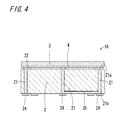
次に、本発明の他の実施形態について説明する。図4は、図2に示した断面図に対応する計測センサ用パッケージ1Aの断面図であり、図5は、図3に示した断面図に対応する計測センサ用パッケージ1Aの断面図である。
Next, another embodiment of the present invention will be described. 4 is a cross-sectional view of the
本実施形態の計測センサ用パッケージ1Aは、上記の実施形態の計測センサ用パッケージ1に対して、基体2が、さらに内部接地導体層25を有する点で異なっており、その他については、同様の構成であるので、同様の構成には計測センサ用パッケージ1と同じ参照符号を付して詳細な説明は省略する。
The
内部接地導体層25は、接地電位に接続され、基体本体20の、第2収容凹部20bの底部と他方主面との間に配設される。内部接地導体層25は、接地ビア導体21と、基体本体20の内部において電気的に接続されており、接地電位が付与される。
The internal
血流の計測等に用いられる計測センサでは、受光素子による受光量が比較的小さいので、受光素子から出力される電気信号は弱く、発光素子に入力される発光制御用の電気信号に比べてノイズによって受ける影響が大きい。 In a measurement sensor used for blood flow measurement or the like, the amount of light received by the light receiving element is relatively small, so the electrical signal output from the light receiving element is weak and noise compared to the electrical signal for light emission control input to the light emitting element. It is greatly affected by.
計測センサは、外部実装基板上に実装されて使用されるが、この外部実装基板の配線を流れる信号等に起因する電磁波が、基体本体20の他方主面側から計測センサ用パッケージ1内に進入して、信号配線導体23を流れる信号にノイズが混入するおそれがある。
The measurement sensor is mounted and used on an external mounting board, and electromagnetic waves caused by signals flowing through the wiring of the external mounting board enter the
上記のように、特に受光素子側は、ノイズの影響を大きく受けるので、外部実装基板からのノイズの影響を抑制するために、受光素子が収容される第2収容凹部20bの底部と他方主面との間に内部接地導体層25を設けている。第2収容凹部20bと外部実装基板との間に内部接地導体層25が位置し、電磁シールドとして機能する。
As described above, particularly on the light receiving element side, it is greatly affected by noise. Therefore, in order to suppress the influence of noise from the external mounting substrate, the bottom and the other main surface of the
本実施形態の計測センサ用パッケージ1Aは、内部接地導体層25を有することで、ノイズによる影響を抑制し、計測精度をさらに向上させることができる。
The
計測センサ用パッケージ1の製造方法について説明する。まず、基体2を公知の多層配線基板の製造方法と同様にして作製する。基体2が、セラミック配線基板であり、セラミック材料がアルミナである場合は、まずアルミナ(Al2O3)やシリカ(SiO2)、カルシア(CaO)、マグネシア(MgO)等の原料粉末に適当な有機溶剤、溶媒を添加混合して泥漿状とし、これを周知のドクターブレード法やカレンダーロール法等によってシート状に成形してセラミックグリーンシート(以下、グリーンシートともいう)を得る。その後、グリーンシートを所定形状に打ち抜き加工するとともに、タングステン(W)とガラス材料等の原料粉末に有機溶剤、溶媒を添加混合して金属ペーストとし、これをグリーンシート表面にスクリーン印刷等の印刷法でパターン印刷する。また、ビア導体は、グリーンシートに貫通孔を設け、スクリーン印刷等によって金属ペーストを貫通孔に充填させる。こうして得られたグリーンシートを複数枚積層し、これを約1600℃の温度で同時焼成することによって基体2が作製される。A method for manufacturing the
一方、ガラス材料を、切削、切断等により所定の形状に切り出した蓋体3を準備し、主面上に、蒸着、スパッタ、焼付け等によって金属薄膜からなる接地導体層4を形成する。このとき、フォトリソグラフィ(ウェットエッチング)法、ドライエッチング法等によって金属薄膜にパターン加工することにより、第1開口4aおよび第2開口4bを形成することができる。
On the other hand, a
次に、本発明の他の実施形態である計測センサ100について説明する。図6は、計測センサ100の構成を示す断面図である。計測センサ100は、上記の計測センサ用パッケージ1,1Aと、第1収容凹部20aに収容される発光素子30と、第2収容凹部20bに収容される受光素子31と、を含む。計測センサ100は、計測センサ用パッケージ1に発光素子30と、受光素子31とを実装し、ボンディングワイヤ32でこれらの素子と接続パッド23aと接続した後、蓋体3を基体本体20に接合して得られる。
Next, the
発光素子30は、VCSEL等の半導体レーザ素子を用いることができ、受光素子31は、シリコンフォトダイオード、GaAsフォトダイオード、InGaAsフォトダイオード、ゲルマニウムフォトダイオード等の各種フォトダイオードを用いることができる。発光素子30および受光素子31は、被計測物の種類、計測するパラメータの種類等により適宜選択すればよい。
The
血流を測定する場合は、例えば、光のドップラー効果を利用して測定するために、発光素子30であるVCSELとして波長が850nmのレーザ光を出射可能なものであればよい。その他の測定を行う場合は、測定目的に応じた波長のレーザ光を出射する発光素子30を選択すればよい。受光素子31は、受光する光が発光素子30から出射されるレーザ光から波長の変化が無い場合、発光素子30の出射光を受光できるものであればよく、波長の変化が有る場合、変化後の波長の光を受光できるものであればよい。
When measuring blood flow, for example, in order to measure using the Doppler effect of light, the VCSEL that is the
発光素子30および受光素子31と接続パッド23aとは、本実施形態では、例えば、ボンディングワイヤ32によって電気的に接続されるが、フリップチップ接続、バンプ接続、異方性導電フィルムを用いた接続等他の接続方法であってもよい。
In the present embodiment, the
計測センサ100は、外部実装基板に実装されて使用される。外部実装基板には、例えば、発光素子30の発光を制御する制御素子、受光素子31の出力信号から血流速度等を算出する演算素子等も実装される。
The
測定する場合には、被計測物として手指の指先を蓋体3の表面に接触させた状態で、外部実装基板から外部接続端子24を介して発光素子制御電流が計測センサ100に入力され、信号ビア導体23b、接続パッド23aを通って発光素子30に入力されて発光素子30から計測用の光が出射される。出射された光が、第1開口4aを通過し、蓋体3を透過して指先に照射されると、血液中の血球細胞で散乱される。蓋体3を透過し、第2開口4bを通過した散乱光が、受光素子31で受光されると、受光量に応じた電気信号が受光素子31から出力される。出力された信号は、接続パッド23a、信号ビア導体23bを通り、外部接続端子24を介して計測センサ100から外部実装基板へと出力される。
In the case of measurement, a light emitting element control current is input from the external mounting substrate to the
外部実装基板では、計測センサ100から出力された信号が、演算素子に入力され、例えば、発光素子30から出射された光である照射光の周波数と、受光素子31が受光した光である散乱光の周波数とに基づいて血流速度を算出することができる。
In the external mounting substrate, the signal output from the
なお、上記では、接地ビア導体21は、基体本体20内で上下方向に一直線状に形成される構成としているが、基体本体20の一方主面から他方主面の外部接続端子24まで電気的に接続されていれば、一直線状でなく、基体本体20内で、内層配線や内部接地導体層25等によってずれて形成されていてもよい。
In the above description, the ground via
また、本実施形態において、環状接地導体層22は、必須構成ではなく、蓋体3に形成された接地導体層4と接地ビア導体21とを直接接合して電気的に接続するように構成してもよい。
In the present embodiment, the annular
また、内部接地導体層25は、基体本体20の、第2収容凹部20bの底部と他方主面との間からさらに面方向に延びて、第1収容凹部20aの底部と他方主面との間に配設されてもよい。
The internal
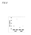
図4,5に示した計測センサ用パッケージ1と同様の構成の計測センサ用パッケージ(誘電体層がアルミナからなり、縦3mm、横4.5mm、厚み1.2mm)を作製し、発光素子30として近赤外線波長のVCSELを、受光素子31として受光径がφ200μmのシリコンフォトダイオードをそれぞれ計測センサ用パッケージに実装して本発明の実施例である計測センサを得た。
A measurement sensor package (dielectric layer is made of alumina,
接地ビア導体21を有しないこと以外は、実施例と同様にして比較例の計測センサを得た。
A comparative measurement sensor was obtained in the same manner as in the example except that the ground via
実施例および比較例の計測センサそれぞれにおいて、蓋体3に手指を接触させない状態で受光素子から出力される信号(パワースペクトル)と、蓋体3に手指を接触させた状態で受光素子から出力される信号(パワースペクトル)と、を測定した。パワースペクトルの測定方法は次のとおりとした。VCSELから発光した光が被測定物に照射され、返ってきた拡散光をフォトダイオードで受光して発生する電流を出力信号とする。出力信号は微弱なため、増幅回路を用いて増幅した後に、AD(アナログ−デジタル)変換し、変換後のデジタル信号をフーリエ変換して、パワースペクトルを得た。
In each of the measurement sensors of the example and the comparative example, a signal (power spectrum) output from the light receiving element without touching the
図7は、実施例および比較例のパワースペクトルの測定結果を示す図である。図7(a)は、比較例の結果を示し、図7(b)は、実施例の結果を示す。また、それぞれの結果において、上側のグラフは、蓋体3に手指を接触させない状態の結果であり、下側のグラフは、蓋体に手指を接触させた状態の結果である。
FIG. 7 is a diagram showing measurement results of the power spectrum of the example and the comparative example. Fig.7 (a) shows the result of a comparative example, FIG.7 (b) shows the result of an Example. Further, in each result, the upper graph is a result in a state where the finger is not brought into contact with the
図7(a)、図7(b)の上側のグラフに示すように、手指を蓋体3に接触させない状態では、実施例および比較例いずれもノイズは発生しなかった。
As shown in the upper graphs of FIGS. 7A and 7B, no noise was generated in both the example and the comparative example in a state where the finger was not in contact with the
図7(a)の下側のグラフに示すように、接地ビア導体21を有していない比較例では、手指が接触した状態では、周波数9kHz〜10kHz付近、および16kHZ付近にノイズが発生した。また、本来検出されるべき血流による散乱に起因する2kHz未満での出力変化は観測されなかった。
As shown in the lower graph of FIG. 7A, in the comparative example not having the ground via
これに対して図7(b)の下側のグラフに示すように、接地ビア導体21を有する実施例では、比較例のようなノイズは発生せず、2kHz以下での出力変化が観測された。
On the other hand, as shown in the lower graph of FIG. 7B, in the example having the ground via
図8は、実施例および比較例の評価結果を示す図である。評価結果として、最大ノイズ量を用いた。最大ノイズ量は、パワースペクトルにおいて、2kHz以上の周波数で最大出力値と最小出力値との差分で算出される。最大ノイズ量が大きいほどノイズの発生が顕著であり、最大ノイズ量が小さいほどノイズの発生が抑制されていると評価できる。 FIG. 8 is a diagram showing the evaluation results of Examples and Comparative Examples. The maximum noise amount was used as the evaluation result. The maximum noise amount is calculated by the difference between the maximum output value and the minimum output value at a frequency of 2 kHz or more in the power spectrum. It can be evaluated that the larger the maximum amount of noise is, the more remarkable the occurrence of noise is, and the smaller the maximum amount of noise is, the more suppressed the generation of noise.
図8に示すように、手指を蓋体3に接触させない状態では、実施例および比較例いずれも最大ノイズ量は小さく、さらに実施例のほうが比較例よりも小さくいことから、実施例は、手指を蓋体3に接触させない状態での微小なノイズも抑制されていることがわかる。また、手指を蓋体3に接触させた状態では、接触させない状態に比べて比較例の最大ノイズ量が大きくなったのに対し、実施例ではわずかに大きくなっただけであった。
As shown in FIG. 8, in the state where the finger is not in contact with the
上記のように、実施例では、接地ビア導体21を有することにより、被計測物の接触によるノイズの発生を抑制し、高精度で血流の計測が可能であることがわかった。
As described above, in the example, it was found that the presence of the ground via
本発明は、その精神または主要な特徴から逸脱することなく、他のいろいろな形態で実施できる。したがって、前述の実施形態はあらゆる点で単なる例示に過ぎず、本発明の範囲は特許請求の範囲に示すものであって、明細書本文には何ら拘束されない。さらに、特許請求の範囲に属する変形や変更は全て本発明の範囲内のものである。 The present invention can be implemented in various other forms without departing from the spirit or main features thereof. Therefore, the above-described embodiment is merely an example in all respects, and the scope of the present invention is shown in the claims, and is not restricted by the text of the specification. Further, all modifications and changes belonging to the scope of the claims are within the scope of the present invention.
1,1A 計測センサ用パッケージ
2 基体
3 蓋体
4 接地導体層
4a 第1開口
4b 第2開口
20 基体本体
20a 第1収容凹部
20b 第2収容凹部
21 接地ビア導体
21a 一方端面
21b 他方端面
22 環状接地導体層
22a ランド部分
22b 接続線部分
23 信号配線導体
23a 接続パッド
23b 信号ビア導体
24 外部接続端子
25 内部接地導体層
30 発光素子
31 受光素子
32 ボンディングワイヤ
100 計測センサDESCRIPTION OF
Claims (5)
前記第1収容凹部および前記第2収容凹部を覆う、絶縁材料からなる板状の蓋体であって、前記第1収容凹部に収容される前記発光素子から出射される光が透過し、前記第2収容凹部に収容される前記受光素子が受光する光が透過する蓋体と、
該蓋体の、前記第1収容凹部および前記第2収容凹部に対向する側の面に配設される、接地電位に接続される接地導体層であって、前記発光素子から出射される光が通過する第1開口および前記受光素子が受光する光が通過する第2開口が設けられており、前記複数の接地ビア導体と電気的に接続される接地導体層と、を含むことを特徴とする計測センサ用パッケージ。A rectangular plate-like base body formed by laminating a plurality of dielectric layers, a first receiving recess for receiving a light emitting element and a second receiving recess for receiving a light receiving element are provided on the first surface. A base body, and one or a plurality of ground via conductors that are disposed outside the first housing recess and the second housing recess and connected to a ground potential in plan view. A substrate;
A plate-like lid made of an insulating material that covers the first housing recess and the second housing recess, and the light emitted from the light emitting element housed in the first housing recess is transmitted, and the first A lid through which light received by the light receiving element housed in the housing recess is transmitted;
A ground conductor layer connected to a ground potential disposed on a surface of the lid that faces the first housing recess and the second housing recess, the light emitted from the light emitting element A first opening that passes therethrough and a second opening through which light received by the light receiving element passes, and a ground conductor layer that is electrically connected to the plurality of ground via conductors. Measurement sensor package.
複数の接地ビア導体は、前記基体本体の第1面の外周に沿って配設され、一方の端面がそれぞれ前記基体の第1面に露出しており、
前記基体は、前記基体本体の前記第1面に、前記第1収容凹部の開口および前記第2収容凹部の開口を取り囲むように環状に設けられる、前記複数の接地ビア導体の各一方の端面を電気的に接続する環状導体層を有することを特徴とする請求項1記載の計測センサ用パッケージ。A plurality of ground via conductors are disposed on the base, and the plurality of ground via conductors are disposed along the outer periphery of the first surface of the base body, and one end surface of each ground via conductor is exposed on the first surface of the base. And
The base is provided with an end surface of each of the plurality of ground via conductors provided on the first surface of the base body in an annular shape so as to surround the opening of the first housing recess and the opening of the second housing recess. The measurement sensor package according to claim 1, further comprising an annular conductor layer that is electrically connected.
前記第1収容凹部に収容される発光素子と、
前記第2収容凹部に収容される受光素子と、を含むことを特徴とする計測センサ。The measurement sensor package according to any one of claims 1 to 4,
A light emitting device housed in the first housing recess,
And a light receiving element housed in the second housing recess.
Applications Claiming Priority (3)
| Application Number | Priority Date | Filing Date | Title |
|---|---|---|---|
| JP2015250656 | 2015-12-22 | ||
| JP2015250656 | 2015-12-22 | ||
| PCT/JP2016/083435 WO2017110291A1 (en) | 2015-12-22 | 2016-11-10 | Measuring sensor package and measuring sensor |
Publications (2)
| Publication Number | Publication Date |
|---|---|
| JPWO2017110291A1 JPWO2017110291A1 (en) | 2018-08-16 |
| JP6483859B2 true JP6483859B2 (en) | 2019-03-13 |
Family
ID=59090416
Family Applications (1)
| Application Number | Title | Priority Date | Filing Date |
|---|---|---|---|
| JP2017557785A Active JP6483859B2 (en) | 2015-12-22 | 2016-11-10 | Measurement sensor package and measurement sensor |
Country Status (6)
| Country | Link |
|---|---|
| US (1) | US11166642B2 (en) |
| EP (2) | EP3395242B1 (en) |
| JP (1) | JP6483859B2 (en) |
| KR (1) | KR102136538B1 (en) |
| CN (2) | CN108135516B (en) |
| WO (1) | WO2017110291A1 (en) |
Families Citing this family (3)
| Publication number | Priority date | Publication date | Assignee | Title |
|---|---|---|---|---|
| WO2017130520A1 (en) * | 2016-01-25 | 2017-08-03 | 京セラ株式会社 | Measurement sensor package and measurement sensor |
| JP6616496B2 (en) * | 2016-04-04 | 2019-12-04 | 京セラ株式会社 | Measurement sensor package and measurement sensor |
| EP3876257A4 (en) * | 2018-10-30 | 2022-08-17 | Kyocera Corporation | Optical sensor device |
Family Cites Families (25)
| Publication number | Priority date | Publication date | Assignee | Title |
|---|---|---|---|---|
| JPS5031895B1 (en) | 1971-03-16 | 1975-10-16 | ||
| JPS5146596B2 (en) * | 1972-09-06 | 1976-12-09 | ||
| JPH0712348B2 (en) * | 1987-02-10 | 1995-02-15 | 松下電器産業株式会社 | Photoelectric pulse wave detector |
| US6300659B1 (en) * | 1994-09-30 | 2001-10-09 | Semiconductor Energy Laboratory Co., Ltd. | Thin-film transistor and fabrication method for same |
| KR100309957B1 (en) * | 1997-09-08 | 2002-08-21 | 신꼬오덴기 고교 가부시키가이샤 | Semiconductor device |
| JP3554886B2 (en) * | 2000-03-30 | 2004-08-18 | 日本特殊陶業株式会社 | Wiring board |
| US6486534B1 (en) * | 2001-02-16 | 2002-11-26 | Ashvattha Semiconductor, Inc. | Integrated circuit die having an interference shield |
| JP2004041482A (en) * | 2002-07-12 | 2004-02-12 | Seiko Epson Corp | Pulse wave detector and biopotential detector |
| JP2005260877A (en) * | 2004-03-15 | 2005-09-22 | Kyocera Corp | High frequency wave module and radio communication device |
| JP4061409B2 (en) * | 2004-11-09 | 2008-03-19 | 国立大学法人九州大学 | Sensor unit and biosensor |
| CN2879968Y (en) * | 2006-02-17 | 2007-03-21 | 杭州大力神医疗器械有限公司 | Photoelectric pulse feeling sensor |
| JP4708214B2 (en) * | 2006-02-23 | 2011-06-22 | 浜松ホトニクス株式会社 | Optical transceiver device |
| EP2277440B1 (en) * | 2008-05-12 | 2014-12-24 | Pioneer Corporation | Self-luminous sensor device |
| WO2009139029A1 (en) * | 2008-05-12 | 2009-11-19 | パイオニア株式会社 | Self-luminous sensor device and method for manufacturing the same |
| JP5549104B2 (en) * | 2008-05-29 | 2014-07-16 | 株式会社リコー | Light emitting device, optical scanning device, and image forming apparatus |
| US20100004518A1 (en) * | 2008-07-03 | 2010-01-07 | Masimo Laboratories, Inc. | Heat sink for noninvasive medical sensor |
| WO2010125705A1 (en) * | 2009-04-30 | 2010-11-04 | 株式会社村田製作所 | Biosensor device |
| JP2010264174A (en) * | 2009-05-18 | 2010-11-25 | Hitachi Cable Ltd | Surface myoelectric potential sensor |
| US8199518B1 (en) * | 2010-02-18 | 2012-06-12 | Amkor Technology, Inc. | Top feature package and method |
| US8258012B2 (en) * | 2010-05-14 | 2012-09-04 | Stats Chippac, Ltd. | Semiconductor device and method of forming discontinuous ESD protection layers between semiconductor die |
| US9490239B2 (en) * | 2011-08-31 | 2016-11-08 | Micron Technology, Inc. | Solid state transducers with state detection, and associated systems and methods |
| TWI453923B (en) * | 2012-06-22 | 2014-09-21 | Txc Corp | Light sensing chip package structure |
| RU2663633C2 (en) * | 2012-12-14 | 2018-08-07 | Конинклейке Филипс Н.В. | Device for measuring physiological parameter of user |
| EP2803315B1 (en) * | 2013-05-15 | 2019-10-02 | Polar Electro Oy | Heart activity sensor structure |
| JP5907200B2 (en) * | 2014-03-18 | 2016-04-26 | セイコーエプソン株式会社 | Photodetection unit and biological information detection apparatus |
-
2016
- 2016-11-10 US US15/770,658 patent/US11166642B2/en active Active
- 2016-11-10 EP EP16878189.6A patent/EP3395242B1/en active Active
- 2016-11-10 CN CN201680060515.8A patent/CN108135516B/en active Active
- 2016-11-10 EP EP21205560.2A patent/EP4026493A1/en not_active Withdrawn
- 2016-11-10 WO PCT/JP2016/083435 patent/WO2017110291A1/en active Application Filing
- 2016-11-10 JP JP2017557785A patent/JP6483859B2/en active Active
- 2016-11-10 KR KR1020187010706A patent/KR102136538B1/en active IP Right Grant
- 2016-11-10 CN CN202011206741.7A patent/CN112168146A/en active Pending
Also Published As
| Publication number | Publication date |
|---|---|
| CN108135516B (en) | 2020-11-20 |
| US20180310836A1 (en) | 2018-11-01 |
| EP4026493A1 (en) | 2022-07-13 |
| JPWO2017110291A1 (en) | 2018-08-16 |
| WO2017110291A1 (en) | 2017-06-29 |
| EP3395242A1 (en) | 2018-10-31 |
| CN112168146A (en) | 2021-01-05 |
| EP3395242A4 (en) | 2019-09-04 |
| US11166642B2 (en) | 2021-11-09 |
| KR20180053383A (en) | 2018-05-21 |
| KR102136538B1 (en) | 2020-07-22 |
| CN108135516A (en) | 2018-06-08 |
| EP3395242B1 (en) | 2021-11-10 |
Similar Documents
| Publication | Publication Date | Title |
|---|---|---|
| JP7061990B2 (en) | Measurement sensor package and measurement sensor | |
| JP6483859B2 (en) | Measurement sensor package and measurement sensor | |
| JP6659377B2 (en) | Measurement sensor package and measurement sensor | |
| JP6999407B2 (en) | Optical sensor device | |
| JP2018100934A (en) | Sensor device | |
| JP6942211B2 (en) | Measurement sensor package and measurement sensor | |
| JP6718339B2 (en) | Measurement sensor package and measurement sensor | |
| JP6462904B2 (en) | Measurement sensor package and measurement sensor | |
| JP7054609B2 (en) | Measurement sensor package and measurement sensor | |
| JP2018196571A (en) | Package for measurement sensor and measurement sensor | |
| JP6666191B2 (en) | Measurement sensor package and measurement sensor | |
| JP2019093078A (en) | Optical sensor device | |
| JP6666192B2 (en) | Measurement sensor package and measurement sensor | |
| JP6753731B2 (en) | Measurement sensor package and measurement sensor | |
| JP6753729B2 (en) | Measurement sensor package and measurement sensor | |
| JP2019058451A (en) | Optical sensor device |
Legal Events
| Date | Code | Title | Description |
|---|---|---|---|
| A621 | Written request for application examination |
Free format text: JAPANESE INTERMEDIATE CODE: A621 Effective date: 20180413 |
|
| TRDD | Decision of grant or rejection written | ||
| A01 | Written decision to grant a patent or to grant a registration (utility model) |
Free format text: JAPANESE INTERMEDIATE CODE: A01 Effective date: 20190115 |
|
| A61 | First payment of annual fees (during grant procedure) |
Free format text: JAPANESE INTERMEDIATE CODE: A61 Effective date: 20190214 |
|
| R150 | Certificate of patent or registration of utility model |
Ref document number: 6483859 Country of ref document: JP Free format text: JAPANESE INTERMEDIATE CODE: R150 |