JP6467801B2 - Spectral image acquisition device and received light wavelength acquisition method - Google Patents
Spectral image acquisition device and received light wavelength acquisition method Download PDFInfo
- Publication number
- JP6467801B2 JP6467801B2 JP2014156542A JP2014156542A JP6467801B2 JP 6467801 B2 JP6467801 B2 JP 6467801B2 JP 2014156542 A JP2014156542 A JP 2014156542A JP 2014156542 A JP2014156542 A JP 2014156542A JP 6467801 B2 JP6467801 B2 JP 6467801B2
- Authority
- JP
- Japan
- Prior art keywords
- light
- wavelength
- light receiving
- spectral
- filter
- Prior art date
- Legal status (The legal status is an assumption and is not a legal conclusion. Google has not performed a legal analysis and makes no representation as to the accuracy of the status listed.)
- Active
Links
- 230000003595 spectral effect Effects 0.000 title claims description 170
- 238000000034 method Methods 0.000 title claims description 49
- 239000000758 substrate Substances 0.000 claims description 66
- 238000003384 imaging method Methods 0.000 claims description 64
- 230000003287 optical effect Effects 0.000 claims description 53
- 238000002834 transmittance Methods 0.000 claims description 31
- 238000001228 spectrum Methods 0.000 claims description 28
- 238000005259 measurement Methods 0.000 claims description 25
- 230000035945 sensitivity Effects 0.000 claims description 25
- 230000008859 change Effects 0.000 claims description 15
- 239000011521 glass Substances 0.000 claims description 6
- 229910018072 Al 2 O 3 Inorganic materials 0.000 claims description 5
- 229910052709 silver Inorganic materials 0.000 claims description 4
- 239000010408 film Substances 0.000 description 108
- 230000008569 process Effects 0.000 description 32
- 238000012545 processing Methods 0.000 description 22
- 238000010586 diagram Methods 0.000 description 16
- 238000009434 installation Methods 0.000 description 14
- 238000003860 storage Methods 0.000 description 10
- 230000007246 mechanism Effects 0.000 description 9
- 230000007423 decrease Effects 0.000 description 8
- 238000004519 manufacturing process Methods 0.000 description 7
- 238000009826 distribution Methods 0.000 description 5
- 230000006870 function Effects 0.000 description 5
- 229910045601 alloy Inorganic materials 0.000 description 4
- 239000000956 alloy Substances 0.000 description 4
- 238000000605 extraction Methods 0.000 description 4
- 239000002184 metal Substances 0.000 description 4
- 229910052751 metal Inorganic materials 0.000 description 4
- 238000004611 spectroscopical analysis Methods 0.000 description 4
- 238000005452 bending Methods 0.000 description 3
- 230000005540 biological transmission Effects 0.000 description 3
- BJQHLKABXJIVAM-UHFFFAOYSA-N bis(2-ethylhexyl) phthalate Chemical compound CCCCC(CC)COC(=O)C1=CC=CC=C1C(=O)OCC(CC)CCCC BJQHLKABXJIVAM-UHFFFAOYSA-N 0.000 description 3
- 238000000701 chemical imaging Methods 0.000 description 3
- 230000001427 coherent effect Effects 0.000 description 3
- 238000007689 inspection Methods 0.000 description 3
- 238000010030 laminating Methods 0.000 description 3
- 239000004973 liquid crystal related substance Substances 0.000 description 3
- 230000002093 peripheral effect Effects 0.000 description 3
- 230000035699 permeability Effects 0.000 description 3
- 229910004298 SiO 2 Inorganic materials 0.000 description 2
- 229910010413 TiO 2 Inorganic materials 0.000 description 2
- 239000006185 dispersion Substances 0.000 description 2
- 238000005530 etching Methods 0.000 description 2
- 239000000463 material Substances 0.000 description 2
- VYPSYNLAJGMNEJ-UHFFFAOYSA-N silicon dioxide Inorganic materials O=[Si]=O VYPSYNLAJGMNEJ-UHFFFAOYSA-N 0.000 description 2
- 229910001316 Ag alloy Inorganic materials 0.000 description 1
- 230000004075 alteration Effects 0.000 description 1
- 238000004458 analytical method Methods 0.000 description 1
- 230000000295 complement effect Effects 0.000 description 1
- 238000012937 correction Methods 0.000 description 1
- 230000003247 decreasing effect Effects 0.000 description 1
- 238000013461 design Methods 0.000 description 1
- KPUWHANPEXNPJT-UHFFFAOYSA-N disiloxane Chemical class [SiH3]O[SiH3] KPUWHANPEXNPJT-UHFFFAOYSA-N 0.000 description 1
- 230000000694 effects Effects 0.000 description 1
- 238000009413 insulation Methods 0.000 description 1
- 239000011159 matrix material Substances 0.000 description 1
- 238000012986 modification Methods 0.000 description 1
- 230000004048 modification Effects 0.000 description 1
- 239000012788 optical film Substances 0.000 description 1
- 239000010453 quartz Substances 0.000 description 1
- 238000011144 upstream manufacturing Methods 0.000 description 1
Images


Classifications
-
- G—PHYSICS
- G01—MEASURING; TESTING
- G01J—MEASUREMENT OF INTENSITY, VELOCITY, SPECTRAL CONTENT, POLARISATION, PHASE OR PULSE CHARACTERISTICS OF INFRARED, VISIBLE OR ULTRAVIOLET LIGHT; COLORIMETRY; RADIATION PYROMETRY
- G01J3/00—Spectrometry; Spectrophotometry; Monochromators; Measuring colours
- G01J3/02—Details
- G01J3/0205—Optical elements not provided otherwise, e.g. optical manifolds, diffusers, windows
- G01J3/0213—Optical elements not provided otherwise, e.g. optical manifolds, diffusers, windows using attenuators
-
- G—PHYSICS
- G01—MEASURING; TESTING
- G01J—MEASUREMENT OF INTENSITY, VELOCITY, SPECTRAL CONTENT, POLARISATION, PHASE OR PULSE CHARACTERISTICS OF INFRARED, VISIBLE OR ULTRAVIOLET LIGHT; COLORIMETRY; RADIATION PYROMETRY
- G01J3/00—Spectrometry; Spectrophotometry; Monochromators; Measuring colours
- G01J3/02—Details
- G01J3/0256—Compact construction
-
- G—PHYSICS
- G01—MEASURING; TESTING
- G01J—MEASUREMENT OF INTENSITY, VELOCITY, SPECTRAL CONTENT, POLARISATION, PHASE OR PULSE CHARACTERISTICS OF INFRARED, VISIBLE OR ULTRAVIOLET LIGHT; COLORIMETRY; RADIATION PYROMETRY
- G01J3/00—Spectrometry; Spectrophotometry; Monochromators; Measuring colours
- G01J3/12—Generating the spectrum; Monochromators
- G01J3/26—Generating the spectrum; Monochromators using multiple reflection, e.g. Fabry-Perot interferometer, variable interference filters
-
- G—PHYSICS
- G01—MEASURING; TESTING
- G01J—MEASUREMENT OF INTENSITY, VELOCITY, SPECTRAL CONTENT, POLARISATION, PHASE OR PULSE CHARACTERISTICS OF INFRARED, VISIBLE OR ULTRAVIOLET LIGHT; COLORIMETRY; RADIATION PYROMETRY
- G01J3/00—Spectrometry; Spectrophotometry; Monochromators; Measuring colours
- G01J3/28—Investigating the spectrum
- G01J3/2803—Investigating the spectrum using photoelectric array detector
- G01J2003/2813—2D-array
-
- G—PHYSICS
- G01—MEASURING; TESTING
- G01J—MEASUREMENT OF INTENSITY, VELOCITY, SPECTRAL CONTENT, POLARISATION, PHASE OR PULSE CHARACTERISTICS OF INFRARED, VISIBLE OR ULTRAVIOLET LIGHT; COLORIMETRY; RADIATION PYROMETRY
- G01J3/00—Spectrometry; Spectrophotometry; Monochromators; Measuring colours
- G01J3/28—Investigating the spectrum
- G01J3/2823—Imaging spectrometer
- G01J2003/2826—Multispectral imaging, e.g. filter imaging
Description
本発明は、分光画像取得装置、及び当該分光画像取得装置における受光波長取得方法に関する。 The present invention relates to a spectral image acquisition apparatus and a received light wavelength acquisition method in the spectral image acquisition apparatus.
従来、互いに対向する一対の反射膜を有するファブリーペローエタロン(干渉フィルター)に入射光を入射させ、干渉フィルターから反射膜間のギャップ寸法に応じた波長の光を面分光させてカメラで撮像する装置が知られている(例えば、特許文献1参照)。
この特許文献1に記載の装置は、反射膜を対向配置させた干渉フィルターの傾斜角を変化させることで、面分光させる光の波長を変化させ、面分光された波長の光を撮像して分光画像を得る。
Conventionally, an apparatus in which incident light is incident on a Fabry-Perot etalon (interference filter) having a pair of reflective films opposed to each other, and light having a wavelength corresponding to the gap size between the reflective films is surface-spectroscopically imaged with a camera. Is known (see, for example, Patent Document 1).
The apparatus described in Patent Document 1 changes the wavelength of light to be subjected to surface spectroscopy by changing the tilt angle of an interference filter having a reflective film disposed oppositely, and images light having a wavelength subjected to surface spectroscopy to perform spectral spectroscopy. Get an image.
ところで、干渉フィルターでは、反射膜間のギャップ寸法に応じて透過光の波長が変化する。しかしながら、干渉フィルターの製造において、この反射膜間のギャップ寸法を均一にすることは困難であり、実際には製造誤差等により、反射膜間のギャップ寸法に面内ばらつきが生じる。上記特許文献1では、このような面内ばらつきが考慮されていないため、干渉フィルターを透過した光は、場所によって透過波長が異なり、即ち、面分光された光の波長が均一にならない(面内ムラが生じる)。
上記のような面内ムラが生じると、カメラを構成する各受光素子において、それぞれ異なる波長の光が受光されてしまい、目標波長の分光画像を精度よく取得することができない。
By the way, in the interference filter, the wavelength of the transmitted light changes according to the gap size between the reflection films. However, in the manufacture of the interference filter, it is difficult to make the gap dimension between the reflection films uniform. Actually, in-plane variation occurs in the gap dimension between the reflection films due to a manufacturing error or the like. In the above-mentioned Patent Document 1, such in-plane variation is not taken into consideration, and thus the light transmitted through the interference filter has a different transmission wavelength depending on the location, that is, the wavelength of the surface-split light is not uniform (in-plane Unevenness occurs).
When the in-plane unevenness as described above occurs, light of different wavelengths is received by each light receiving element constituting the camera, and a spectral image of the target wavelength cannot be obtained with high accuracy.
本発明は、高精度な分光画像を取得可能な分光画像取得装置、及び当該分光画像取得装置における受光波長取得方法を提供することを目的とする。 An object of this invention is to provide the spectral image acquisition apparatus which can acquire a highly accurate spectral image, and the light reception wavelength acquisition method in the said spectral image acquisition apparatus.
本発明に係る一適用例の分光画像取得装置は、一対の反射膜を有し、入射光を分光する分光フィルターと、複数の受光素子を有し、前記分光フィルターにより分光された光を受光する撮像部と、リファレンス光を前記撮像部で受光した際に、前記複数の受光素子の各々から出力される信号値に基づいて、前記複数の受光素子の各々に入射した光の中心波長を取得する波長取得部と、を備え、前記リファレンス光に含まれる所定波長域における複数の波長成分の各々の光量は、前記リファレンス光の光軸に対して交差する面内において略均一であり、前記リファレンス光の前記所定波長域における複数の波長成分の各々の光を前記撮像部で受光させた際に前記受光素子から出力される信号値は、波長成分毎に異なり、前記波長取得部は、前記撮像部で前記リファレンス光を受光した際に、前記複数の受光素子のそれぞれから出力される、前記一対の反射膜のギャップ寸法の変化に応じた信号値に基づいて、前記複数の受光素子の各々に入射した光の中心波長を取得することを特徴とする。 A spectral image acquisition apparatus according to an application example of the present invention includes a pair of reflective films, includes a spectral filter that splits incident light, and a plurality of light receiving elements, and receives the light that is spectrally separated by the spectral filter. When the imaging unit and the reference light are received by the imaging unit, a center wavelength of light incident on each of the plurality of light receiving elements is acquired based on a signal value output from each of the plurality of light receiving elements. comprising a wavelength obtaining unit, the light quantity of each of the plurality of wavelength components in a predetermined wavelength band included in the reference light is substantially uniform in a plane intersecting the optical axis of the reference light, the reference light wherein said signal value output from the light receiving element of light of each of the plurality of wavelength components in was received by the imaging unit in a predetermined wavelength region, varies for each wavelength component, the wavelength acquisition unit, the shooting of Each of the plurality of light receiving elements based on a signal value that is output from each of the plurality of light receiving elements and corresponding to a change in a gap dimension of the pair of reflective films when the reference light is received by the unit. The center wavelength of the incident light is acquired .
本適用例では、波長取得部は、撮像部により、分光フィルターを透過又は反射したリファレンス光を受光し、当該撮像部の各受光素子から出力される信号値に基づいて、各受光素子で受光された光の中心波長を取得する。
ここで、本適用例のリファレンス光は、各波長成分の光量が面内において略均一であり、分光フィルターにリファレンス光を入射させた際に入射位置によって光量値が変化することがない。例えば、リファレンス光に含まれる波長λ1の光は、分光フィルターの入射する位置によらず同じ光量Aとなる。この場合、分光フィルターにおける入射光の入射領域内で、分光される光の波長にムラがない(面内ムラがない)場合、分光フィルターから波長λ1の光を透過させると、撮像部の各受光素子において光量Aに対応した信号値が出力される。
また、本適用例において、リファレンス光を受光素子で受光させた際に、波長成分毎に受光素子から出力される信号値が異なる。すなわち、波長λ1の光を受光素子で受光させた際の信号値と、波長λ2の光を受光素子で受光させた際の信号値はそれぞれ異なる値となる。
In this application example, the wavelength acquisition unit receives the reference light transmitted or reflected by the spectral filter by the imaging unit, and is received by each light receiving element based on the signal value output from each light receiving element of the imaging unit. Get the center wavelength of the light.
Here, in the reference light of this application example, the light amount of each wavelength component is substantially uniform in the plane, and the light amount value does not change depending on the incident position when the reference light is incident on the spectral filter. For example, the light of wavelength λ1 included in the reference light has the same light amount A regardless of the position where the spectral filter is incident. In this case, if there is no unevenness in the wavelength of the light to be dispersed within the incident light incident region in the spectral filter (there is no in-plane unevenness), if light having a wavelength λ1 is transmitted from the spectral filter, A signal value corresponding to the light amount A is output from the element.
In this application example, when the reference light is received by the light receiving element, the signal value output from the light receiving element is different for each wavelength component. That is, the signal value when the light of the wavelength λ1 is received by the light receiving element is different from the signal value when the light of the wavelength λ2 is received by the light receiving element.
このような構成では、分光フィルターから出射(透過又は反射)されたリファレンス光を各受光素子で受光すると、受光された光の中心波長に応じた信号値が出力されることになる。よって、所定光量のリファレンス光の各波長成分に対して、受光素子から出力される信号値を予め測定しておくことで、波長取得部は、容易かつ精度よく各受光素子において受光された光の中心波長を取得することができる。
このように、各受光素子で受光される光の中心波長が取得されることで、撮像画像における波長分布を判定することができ、波長補正を行うことで高精度な分光画像を撮像することができる。例えば、各受光素子で目標波長の光を受光できるように分光フィルターから出射させる光の波長を順次変更し、各受光素子における目標波長の光の光量をそれぞれ検出した後、これらを例えば合成することで、目標波長の分光画像を取得することが可能となる。
In such a configuration, when the reference light emitted (transmitted or reflected) from the spectral filter is received by each light receiving element, a signal value corresponding to the center wavelength of the received light is output. Therefore, by measuring in advance the signal value output from the light receiving element for each wavelength component of the reference light of a predetermined light amount, the wavelength acquisition unit can easily and accurately receive the light received by each light receiving element. The center wavelength can be acquired.
Thus, by acquiring the center wavelength of the light received by each light receiving element, the wavelength distribution in the captured image can be determined, and a highly accurate spectral image can be captured by performing wavelength correction. it can. For example, the wavelength of light emitted from the spectral filter is sequentially changed so that each light receiving element can receive light of the target wavelength, and the amount of light of the target wavelength in each light receiving element is detected, and then combined, for example. Thus, a spectral image of the target wavelength can be acquired.
本適用例の分光画像取得装置において、前記撮像部に入射される光の光路上に配置される固定フィルターを備え、前記固定フィルターは、前記所定波長域における前記複数の波長成分の各々に対して、異なる透過率を有することが好ましい。 In the spectral image acquisition device according to this application example, the spectral image acquisition device includes a fixed filter disposed on an optical path of light incident on the imaging unit, and the fixed filter is provided for each of the plurality of wavelength components in the predetermined wavelength region. preferably it has a different transmittance.
本適用例では、各波長成分に対する透過率がそれぞれ異なる固定フィルターと、分光フィルターとを介した光が撮像部で受光される。
例えば、リファレンス光の波長特性が略一定(各波長の光量が均一)である場合や受光素子の波長に対する感度が略一定である場合、固定フィルターが設けられていない場合、各受光素子から出力される信号値が波長成分毎に近い値となり、受光された光の中心波長の判定が困難となる場合がある。これに対して、本適用例では、上記のような固定フィルターを用いることで、各受光素子からの信号値が波長成分毎に異なる値となる。従って、より精度よく受光素子で受光された光の中心波長を取得することができる。
In this application example, the light transmittance through the different fixed filters, respectively, and a spectral filter for each wavelength component is received by the imaging unit.
For example, if sensitivity to the wavelength of the case and the light receiving element wavelength characteristics of the reference light is substantially constant (the light amount of each wavelength uniform) is substantially constant, when the fixed filter is not provided, the output from the light receiving element The signal value to be obtained is a value close to each wavelength component, and it may be difficult to determine the center wavelength of the received light. On the other hand, in this application example, by using the fixed filter as described above, the signal value from each light receiving element becomes a different value for each wavelength component. Therefore, the center wavelength of the light received by the light receiving element can be obtained with higher accuracy.
本適用例の分光画像取得装置において、前記リファレンス光を出射する光源を有し、前記光源は、前記所定波長域における前記複数の波長成分の各々に対して、異なる光量の光を出射することが好ましい。 The spectroscopic image acquisition device of this application example includes a light source for emitting the reference light, the light source for each of the plurality of wavelength components in the predetermined wavelength range, it emits light of a different quantity Is preferred.
本適用例では、光源から出射されるリファレンス光の各波長における光量がそれぞれ異なっている。
例えば、リファレンス光の波長特性が略一定(各波長の光量が均一)である場合や受光素子の波長に対する感度が略一定である場合、各受光素子から出力される信号値が波長成分毎に近い値となり、受光された光の中心波長の判定が困難となる場合がある。これに対して、本適用例では、上記のように光源から射出される各波長の光量がそれぞれ異なるため、各受光素子からの信号値が波長成分毎に異なる値となる。この場合、上記適用例のように固定フィルターを用いることなく、リファレンス光を受光した際の各受光素子から出力される信号値が異なる値となり、精度よく受光素子で受光された光の中心波長を取得することができる。
また、上記適用例のように固定フィルターを用いる場合であっても、光源から出射されるリファレンス光の波長特性と、固定フィルターの透過率とを掛けあわせた際に、各波長成分でそれぞれ異なる光量となるように、光源及び固定フィルターの特性を設定すればよい。
In this application example, the amount of light at each wavelength of the reference light emitted from the light source is different.
For example, if sensitivity to the wavelength of the case and the light receiving element wavelength characteristics of the reference light is substantially constant (the light amount of each wavelength uniform) is substantially constant, the signal value for each wavelength component output from the light receiving elements It becomes a close value, and it may be difficult to determine the center wavelength of the received light. On the other hand, in this application example, since the light amounts of the respective wavelengths emitted from the light sources are different as described above, the signal values from the respective light receiving elements are different values for each wavelength component. In this case, the signal value output from each light receiving element when receiving the reference light is different without using a fixed filter as in the above application example, and the center wavelength of the light received by the light receiving element is accurately determined. Can be acquired.
Further, even in the case of using the fixed filter as the application example, the wavelength characteristic of the reference light emitted from the light source, when combined over the transmittance of the fixed filter, the amount of light different from each other in each wavelength component What is necessary is just to set the characteristic of a light source and a fixed filter so that it may become.
本適用例の分光画像取得装置において、前記撮像部における前記複数の受光素子の各々は、前記波長成分毎に異なる感度を有することが好ましい。 The spectroscopic image acquisition device of this application example, each of the plurality of light receiving elements in the image pickup unit may have a different sensitivity for each of the wavelength components.
本適用例では、撮像部の受光素子における受光感度が各波長でそれぞれ異なっている。
例えば、リファレンス光の波長特性が略一定(各波長の光量が均一)である場合や受光素子の波長に対する感度が略一定である場合、信号値が波長成分毎に近い値となり、受光された光の中心波長の判定が困難となる場合がある。これに対して、本適用例では、上記のように各受光素子の感度が波長毎に異なるため、リファレンス光における各波長成分の光量が略一定でも、各受光素子からの信号値が波長成分毎に異なる値となる。この場合でも、上記適用例のように固定フィルターを用いることなく、リファレンス光を受光した際の各受光素子から出力される信号値が異なる値となり、精度よく受光素子で受光された光の中心波長を取得することができる。
また、上記適用例のように固定フィルターを用いてもよく、リファレンス光の光量を波長成分毎に異ならせてもよい。この場合、例えば、固定フィルターの透過率と、光源から出射されるリファレンス光の波長特性と、受光素子の感度とを掛けあわせた際に、受光素子から各波長成分でそれぞれ異なる信号値が出力されるように、光源、固定フィルター、及び受光素子の特性を設定すればよい。
In this application example, the light receiving sensitivity of the light receiving element of the imaging unit is different for each wavelength.
For example, if sensitivity to the wavelength of the case and the light receiving element wavelength characteristics of the reference light is substantially constant (the light amount of each wavelength uniform) is substantially constant, the signal value becomes a value close to each wavelength component, which is received It may be difficult to determine the center wavelength of light. On the other hand, in this application example, since the sensitivity of each light receiving element is different for each wavelength as described above, even if the light amount of each wavelength component in the reference light is substantially constant, the signal value from each light receiving element is different for each wavelength component. It becomes a different value. Even in this case, the signal value output from each light receiving element when receiving the reference light becomes a different value without using a fixed filter as in the above application example, and the center wavelength of the light received by the light receiving element with high accuracy Can be obtained.
In addition, a fixed filter may be used as in the above application example, and the amount of reference light may be different for each wavelength component. In this case, for example, the transmittance of the fixed filter, the wavelength characteristic of the reference light emitted from the light source, when combined over the sensitivity of the light receiving elements, different signal values output from the light receiving element at each wavelength component Thus, the characteristics of the light source, the fixed filter, and the light receiving element may be set.
本適用例の分光画像取得装置において、前記リファレンス光の前記所定波長域における前記複数の波長成分の各々を前記撮像部で受光させた際に前記受光素子から出力される信号値は、波長に対して単調変化することが好ましい。 The spectroscopic image acquisition device of this application example, the signal value outputted from the light receiving element each of the plurality of wavelength components in the predetermined wavelength range of the reference light upon is received by the imaging section, the wave length On the other hand, it is preferable to change monotonously.
本適用例では、リファレンス光を撮像部で受光した際に、各波長成分に対する受光素子から出力される信号値が、波長に対して単調変化する。
つまり、リファレンス光における所定波長域に含まれる波長を順次切り替えて、それぞれ個別に受光素子で受光させた際に、受光素子から出力される信号値が単調増加又は単調減少するように、リファレンス光の波長特性や、受光素子の感度、又は固定フィルターの透過率が設定されている。
この場合、分光フィルターを介してリファレンス光を受光素子で受光した際に、信号値に対して対応する波長が1つに決まることになり、より精度よく受光素子で受光された光の中心波長を特定することができる。また、波長変化に対する信号値変化が単調変化するため、例えば補完処理等により出力された信号値から受光素子で受光された光の中心波長を容易に算出することもできる。
In this application example, upon receiving the reference light by the imaging unit, the signal value output from the light receiving element for each wavelength component, it varies monotonically for the wave length.
In other words, when the wavelength included in the predetermined wavelength range in the reference light is sequentially switched and individually received by the light receiving element, the signal value output from the light receiving element is monotonously increased or decreased monotonously. and wavelength characteristics, sensitivity of the light receiving element, or the transmittance of the fixed filter is set.
In this case, when the reference light is received by the light receiving element via the spectral filter, the wavelength corresponding to the signal value is determined to be one, and the center wavelength of the light received by the light receiving element is more accurately determined. Can be identified. Further, since the signal value change with respect to the wavelength change monotonously changes, for example, the center wavelength of the light received by the light receiving element can be easily calculated from the signal value output by the complementary processing or the like.
本適用例の分光画像取得装置において、前記撮像部に入射される光の光路上に配置される固定フィルターを備え、前記固定フィルターは、ガラス基板にAg及びAl2O3を積層させたフィルターであることが好ましい。 In the spectral image acquisition device according to this application example, the fixed image filter includes a fixed filter disposed on an optical path of light incident on the imaging unit, and the fixed filter is a filter in which Ag and Al 2 O 3 are stacked on a glass substrate. Preferably there is.
本適用例では、別途固定フィルターを用いて波長に対して信号値を単調変化させる際に、固定フィルターとして、ガラス基板にAg及びAl2O3を積層させたフィルターを用いる。
このような固定フィルターでは、波長を単調増加させた際に、透過率が単調減少する。従って、リファレンス光を出力する光源における波長特性や、受光素子の感度の設定が困難である場合でも、リファレンス光を受光した際の受光素子からの信号値を波長に対して単調増加させることができる。
In this application example, when to monotonically changing the signal value for the wavelength with a separate fixed filters, a fixed filter, using a filter as a laminate of Ag and Al 2 O 3 in the glass substrate.
In such fixed filter, when allowed to monotonically increasing wavelength, transmittance decreases monotonically. Accordingly, and wavelength characteristics of the light source that outputs a reference light, even if the setting of the sensitivity of the light receiving element is difficult, is possible to monotonically increase the signal value from the light receiving element at the time of receiving the reference light to the wavelength it can.
本適用例の分光画像取得装置において、前記分光フィルターは、出射させる光の波長を変更可能であり、前記分光画像取得装置は、さらに、前記分光フィルターが分光する光の波長を変化させる測定制御部と、前記複数の受光素子の各々で受光された同一波長の光の光量に基づいて、当該同一波長に対する分光画像を生成する画像生成部と、を備えていることが好ましい。 In the spectral image acquisition device according to this application example, the spectral filter can change a wavelength of light to be emitted, and the spectral image acquisition device can further change a wavelength of light that is split by the spectral filter. When the plurality of based on the amount of light of the same wavelength of light received by each light receiving element, is preferably provided with an image generator that generates a spectral image, the relative equivalents of identity wave.
本適用例では、測定制御部により分光フィルターから出射させる(分光させる)光の波長を順次変化させて、各受光素子での光量を取得する。この際、目標波長の分光画像の各画素の光量が得られるように、順次ギャップ寸法を変化させる。そして、画像生成部は、各受光素子で受光された目標波長の光の光量に基づいて、分光画像を生成する。これにより、所望の目標波長の光の光量を各画素の画素値(例えば輝度値)とした分光画像を合成することができる。 In this application example, the light intensity at each light receiving element is acquired by sequentially changing the wavelength of light emitted (split) from the spectral filter by the measurement control unit. At this time, the gap size is sequentially changed so that the light quantity of each pixel of the spectral image of the target wavelength can be obtained. Then, the image generation unit generates a spectral image based on the amount of light of the target wavelength received by each light receiving element. Thereby, it is possible to synthesize a spectral image in which the amount of light of a desired target wavelength is the pixel value (for example, luminance value) of each pixel.
本適用例の分光画像取得装置において、前記複数の受光素子の各々で受光される光の分光スペクトルを測定するスペクトル測定部を備えていることが好ましい。
本発明では、分光フィルターから出射させる光の波長を順次切り替え、各波長に対する各受光素子での受光量に基づき、各受光素子で受光された光の分光スペクトルを測定する。このような構成では、各受光素子に対応した各画素における正確な分光スペクトルを取得することができる。
In the spectral image acquisition device of this application example, it is preferable that a spectral measurement unit that measures a spectral spectrum of light received by each of the plurality of light receiving elements is provided.
In the present invention, the wavelength of light emitted from the spectral filter is sequentially switched, and the spectral spectrum of the light received by each light receiving element is measured based on the amount of light received by each light receiving element for each wavelength. In such a configuration, it is possible to acquire an accurate spectral spectrum in each pixel corresponding to each light receiving element.
本適用例の分光画像取得装置において、前記画像生成部は、前記複数の受光素子の各々で受光される光の分光スペクトルに基づいて、前記複数の受光素子の各々にて受光された前記同一波長の光に対する光量を取得し、当該同一波長に対する分光画像を生成することが好ましい。
本適用例では、上記発明のように測定された各分光素子に対応した各画素における分光スペクトルに基づいて、分光画像を生成する。すなわち、各画素の分光スペクトルから所望の目標波長の光量を検出し、これらの光量に基づいて目標波長の分光画像を生成する。この場合、取得した分光画像が複数ある場合(目標波長が複数ある場合)や、撮像操作の後に目標波長を設定する場合において、撮像操作を繰り返す必要がなく、容易に所望の目標波長の分光画像を取得できる。
The spectroscopic image acquisition device of this application example, the image generation unit based on the spectrum of light received by each of the plurality of light receiving elements, before Symbol same which is received by each of the plurality of light receiving elements Gets the amount with respect to light having a wave, it is preferable to produce a spectral image for those of identity-wave.
In this application example, a spectroscopic image is generated based on the spectroscopic spectrum in each pixel corresponding to each spectroscopic element measured as in the above invention. That is, the light amount of a desired target wavelength is detected from the spectral spectrum of each pixel, and a spectral image of the target wavelength is generated based on these light amounts. In this case, when there are a plurality of acquired spectral images (when there are a plurality of target wavelengths) or when a target wavelength is set after the imaging operation, it is not necessary to repeat the imaging operation, and a spectral image of a desired target wavelength can be easily obtained. Can be obtained.
本適用例の分光画像取得装置において、前記波長取得部により取得された前記複数の受光素子の各々で受光された光の中心波長に基づいて、前記複数の受光素子の各々に入射する光の入射角を取得する入射角取得部を備えていることが好ましい。
本適用例では、波長取得部により取得された各受光素子で受光された光の中心波長に基づいて、受光素子に入射する光の入射角を取得する。つまり、上述した本発明における適用例では、受光素子で受光された光は、分光フィルターにおける面内ばらつきや入射角のばらつきを含んだ光となり、これらを考慮して最終的にどの波長の光が受光されたかを判定することが可能となる。従って、例えば、平行光となるリファレンス光を各受光素子で受光した際の信号値から面内ばらつきを考慮した中心波長を特定した後、入射光学系等を介在させた測定を実施し、波長シフト量を判定することで、入射光学系による入射角のバラつきを測定することができる。
このような分光測定装置では、例えば、入射光学系の各レンズの入射角のバラつき検査等に適用することができる。
In the spectral image acquisition device according to this application example, the incidence of light incident on each of the plurality of light receiving elements based on the center wavelength of the light received by each of the plurality of light receiving elements acquired by the wavelength acquisition unit. It is preferable that an incident angle acquisition unit that acquires an angle is provided.
In this application example, the incident angle of light incident on the light receiving element is acquired based on the center wavelength of the light received by each light receiving element acquired by the wavelength acquisition unit. That is, in the application example of the present invention described above, the light received by the light receiving element becomes a contained variations in the plane variation and angle of incidence in the spectral filter light and these considerations end what wavelength light It is possible to determine whether light has been received. Therefore, for example, after specifying the center wavelength considering the in-plane variation from the signal value when the reference light that becomes parallel light is received by each light receiving element, the measurement is performed through the incident optical system and the wavelength shift is performed. By determining the amount, the variation in the incident angle by the incident optical system can be measured.
Such a spectroscopic measurement apparatus can be applied to, for example, inspection of variations in the incident angle of each lens of the incident optical system.
本適用例の分光画像取得装置において、前記分光フィルターは、互いに対向する一対の反射膜、及び前記一対の反射膜間のギャップ寸法を変更するギャップ変更部を有する波長可変干渉フィルターであることが好ましい。
本適用例では、分光フィルターとして波長可変干渉フィルターを用いる。このような波長可変干渉フィルターは、例えば、AOTF(Acousto-Optic Tunable Filter)やLCTF(Liquid Crystal Tunable Filters)等の分光フィルターに対して薄型化、小型化が可能であり、分光画像取得装置の小型化を図れる。
In the spectral image acquisition device of this application example, the spectral filter is preferably a wavelength variable interference filter having a pair of reflective films facing each other and a gap changing unit that changes a gap size between the pair of reflective films. .
In this application example, a wavelength variable interference filter is used as the spectral filter. Such a wavelength tunable interference filter can be made thinner and smaller than a spectral filter such as AOTF (Acousto-Optic Tunable Filter) or LCTF (Liquid Crystal Tunable Filters). Can be realized.
本発明の一適用例の受光波長取得方法は、一対の反射膜を有して入射光を分光する分光フィルター、及び、複数の受光素子を有して前記分光フィルターにより分光された光を受光する撮像部を備えた分光画像取得装置における受光波長取得方法であって、リファレンス光を、前記分光フィルターを介して前記撮像部に受光させる第一ステップと、前記撮像部で受光した際に前記複数の受光素子の各々から出力される信号値に基づいて、前記複数の受光素子の各々に入射した光の中心波長を取得する第二ステップと、を含み、前記リファレンス光に含まれる所定波長域における複数の波長成分の各々の光量が前記リファレンス光の光軸に対して交差する面内において略均一であり、前記分光フィルターを介して前記リファレンス光の前記所定波長域における前記複数の波長成分の各々の光を前記撮像部で受光させた際に前記受光素子から出力される信号値は、波長成分毎で異なり、前記第二ステップでは、前記撮像部で前記リファレンス光を受光した際に、前記複数の受光素子のそれぞれから出力される、前記一対の反射膜のギャップ寸法の変化に応じた信号値に基づいて、前記複数の受光素子の各々に入射した光の中心波長を取得することを特徴とする。 A method for obtaining a received wavelength of an application example of the present invention includes a spectral filter that has a pair of reflective films and splits incident light, and a light that has a plurality of light receiving elements and is spectrally separated by the spectral filter. A light reception wavelength acquisition method in a spectral image acquisition device including an imaging unit, wherein a first step of causing a reference light to be received by the imaging unit via the spectral filter, and the plurality of the plurality of light sources when the imaging unit receives the reference light A second step of acquiring a center wavelength of light incident on each of the plurality of light receiving elements based on a signal value output from each of the light receiving elements, and a plurality of signals in a predetermined wavelength range included in the reference light The wavelength components of the reference light are substantially uniform in a plane intersecting the optical axis of the reference light, and the predetermined wave of the reference light passes through the spectral filter. Signal values output each of the light of said plurality of wavelength components in frequency from the light receiving element when the is received by the imaging section, different for each wavelength component, and in the second step, the by the image pickup unit Light incident on each of the plurality of light receiving elements based on a signal value output from each of the plurality of light receiving elements and corresponding to a change in the gap dimension of the pair of reflection films when receiving the reference light The center wavelength is acquired .
本適用例では、撮像部により分光フィルターを透過又は反射したリファレンス光を受光し、当該撮像部の各受光素子から出力される信号値に基づいて、各受光素子で受光された光の中心波長を取得する。ここで、上記適用例と同様、リファレンス光は、各波長成分の光量が面内において略均一であり、分光フィルターにリファレンス光を入射させた際に入射位置によって光量値が変化することがない。また、リファレンス光を受光素子で受光させた際に、波長成分毎に受光素子から出力される信号値が異なる。
従って、分光フィルターから出射(透過又は反射)されたリファレンス光を各受光素子で受光すると、受光された光の中心波長に応じた信号値が出力されることになり、例えば受光素子から出力される信号値を予め測定しておくことで、容易かつ精度よく各受光素子において受光された光の中心波長を取得することができる。
In this application example, the reference light transmitted or reflected by the spectral filter by the imaging unit is received, and the center wavelength of the light received by each light receiving element is determined based on the signal value output from each light receiving element of the imaging unit. get. Here, as in the application example described above, the light amount of each wavelength component of the reference light is substantially uniform in the plane, and the light amount value does not change depending on the incident position when the reference light is incident on the spectral filter. Further, when the reference light is received by the light receiving element, the signal value output from the light receiving element is different for each wavelength component.
Therefore, when the reference light emitted (transmitted or reflected) from the spectral filter is received by each light receiving element, a signal value corresponding to the center wavelength of the received light is output, for example, output from the light receiving element. By measuring the signal value in advance, the center wavelength of the light received by each light receiving element can be acquired easily and accurately.
[第一実施形態]
以下、本発明に係る第一実施形態について、図面に基づいて説明する。
[分光カメラの概略構成]
図1は、本発明の第一実施形態に係る分光カメラの概略構成を示す概略図である。
分光カメラ1は、本発明の分光画像取得装置に相当し、撮像対象の分光画像を撮像する装置である。
[First embodiment]
Hereinafter, a first embodiment according to the present invention will be described with reference to the drawings.
[Schematic configuration of spectroscopic camera]
FIG. 1 is a schematic diagram showing a schematic configuration of the spectroscopic camera according to the first embodiment of the present invention.
The spectroscopic camera 1 corresponds to the spectroscopic image acquisition device of the present invention, and is a device that captures a spectroscopic image to be imaged.
分光カメラ1は、図1に示すように、光源部12と、撮像モジュール13と、ディスプレイ14と、操作部15と、制御部16と、を備え、これらの各構成が外装筐体11に収納されている。このような分光カメラ1としては、例えばカメラ機能を備えた既存の各種装置を例示でき、例えば、スマートフォンやタブレット端末、デジタルカメラ等を用いることができる。
As shown in FIG. 1, the spectroscopic camera 1 includes a
[光源部の構成]
光源部12は、測定対象に対して光を照射する装置である。
本実施形態では、光源部12から出射されたリファレンス光が、反射率が既知である基準板(例えば白色板等)で反射され、当該反射光が撮像モジュール13にて撮像された際に撮像モジュールから出力される信号値に基づいて、受光された光の中心波長を取得する。本実施形態では、説明の簡略化のため、リファレンス光は、分光画像の取得対象となる所定波長域(以降、分光波長域と称する)における各波長成分の光量が一定、若しくは略一定の光であり、光量の面内ばらつきがない光である例を示す。
[Configuration of light source section]
The
In the present embodiment, the reference light emitted from the
[撮像モジュールの構成]
撮像モジュール13は、入射光を受光して画像を取得する。この撮像モジュール13は、入射光学系131と、固定フィルター132と、本発明の分光フィルターである波長可変干渉フィルター5と、撮像部133と、フィルター駆動回路134と、を備えている。
[Image module configuration]
The
[入射光学系の構成]
入射光学系131は、外装筐体11に設けられた入射窓から入射した光(対象物の像)を撮像部133に結像する。この入射光学系131としては、例えば、波長可変干渉フィルター5に対して、光の主光軸が平行となるように入射光を導くテレセントリック光学系等を例示できる。
[Configuration of incident optical system]
The incident
[固定フィルターの構成]
固定フィルター132は、所定の透過率特性を有し、当該透過率特性に基づいた光量の光を透過させる。
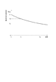
図2は、本実施形態の固定フィルターの透過率特性を示す図である。
図2に示すように、本実施形態の固定フィルター132は、分光波長域の各波長成分に対してそれぞれ異なる透過率特性を有する。より具体的には、固定フィルター132は、波長増加方向に対して、透過率が単調減少する透過率特性を有する。このような固定フィルター132としては、例えば、ガラス基板に対して20nmのAg膜と、20nmのAl2O3を積層させた積層体を用いることで、容易に製造することができる。
[Configuration of fixed filter]
The fixed
FIG. 2 is a diagram showing the transmittance characteristics of the fixed filter of the present embodiment.
As shown in FIG. 2, the fixed
また、固定フィルター132には、進退機構132Aが設けられている。この進退機構132Aは、制御部16の制御により駆動され、固定フィルター132を入射光学系131から入射される光の光路に対して進退させる。すなわち、進退機構132Aは、撮像部133の各受光素子133Aで受光される光の中心波長を特定する際には、固定フィルター132を光路上に配置し、撮像対象の分光画像を撮像する際には、固定フィルター132を光路上から退避させる。
The fixed
[撮像部の構成]
撮像部133は、例えばCCDやCMOS等のイメージセンサー等を用いることができる。撮像部133は、撮像画像の各画素に対応した受光素子133Aがマトリクス状に配置された2次元アレイ構造を有する。そして、各受光素子133Aは、受光された光量に基づいた信号値を制御部16に出力する。
なお、本実施形態において、説明の簡略化のため、各受光素子における感度は一定であり、かつ分光波長域における各波長成分における感度も一定であるとする。
[Configuration of imaging unit]
For the
In the present embodiment, for simplification of description, it is assumed that the sensitivity of each light receiving element is constant and the sensitivity of each wavelength component in the spectral wavelength range is also constant.
[波長可変干渉フィルターの構成]
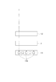
図3は、波長可変干渉フィルター5の概略構成を示す平面図である。図4は、図3のB−B線で切断した波長可変干渉フィルター5の概略構成を示す断面図である。
波長可変干渉フィルター5は、図3及び図4に示すように、固定基板51及び可動基板52を備えている。これらの固定基板51及び可動基板52は、それぞれ例えば各種ガラスや、水晶等により形成されており、本実施形態では、石英ガラスにより構成されるものとする。そして、これらの基板51,52は、図4に示すように、接合膜53(第一接合膜531及び第二接合膜532)により接合されることで、一体的に構成されている。具体的には、固定基板51の第一接合部513、及び可動基板52の第二接合部523が、例えばシロキサンを主成分とするプラズマ重合膜等により構成された接合膜53により接合されている。
なお、以降の説明に当たり、固定基板51又は可動基板52の基板厚み方向から見た平面視、つまり、固定基板51、接合膜53、及び可動基板52の積層方向から波長可変干渉フィルター5を見た平面視を、フィルター平面視と称する。
[Configuration of wavelength tunable interference filter]
FIG. 3 is a plan view showing a schematic configuration of the variable
The wavelength
In the following description, the wavelength
固定基板51には、図4に示すように、本発明の一対の反射膜の一方を構成する固定反射膜54が設けられている。また、可動基板52には、本発明の一対の反射膜の他方を構成する可動反射膜55が設けられている。これらの固定反射膜54及び可動反射膜55は、反射膜間ギャップG1を介して対向配置されている。
そして、波長可変干渉フィルター5には、反射膜54,55間のギャップG1の距離(ギャップ寸法)を調整するのに用いられる、本発明のギャップ変更部である静電アクチュエーター56が設けられている。この静電アクチュエーター56は、固定基板51に設けられた固定電極561と、可動基板52に設けられた可動電極562と、を備え、各電極561,562が対向することにより構成されている。これらの固定電極561,可動電極562は、電極間ギャップを介して対向する。ここで、これらの電極561,562は、それぞれ固定基板51及び可動基板52の基板表面に直接設けられる構成であってもよく、他の膜部材を介して設けられる構成であってもよい。
なお、本実施形態では、反射膜間ギャップG1が電極間ギャップよりも小さく形成される構成を例示するが、例えば波長可変干渉フィルター5により透過させる波長域によっては、反射膜間ギャップG1を電極間ギャップよりも大きく形成してもよい。
また、フィルター平面視において、可動基板52の一辺側(例えば、図3における辺C3−C4)は、固定基板51の辺C3´−C4´よりも外側に突出する。この可動基板52の突出部分は、固定基板51と接合されない電装部526であり、波長可変干渉フィルター5を固定基板51側から見た際に露出する面は、後述する電極パッド564P,565Pが設けられる電装面524となる。
同様に、フィルター平面視において、固定基板51の一辺側(電装部526とは反対側)は、可動基板52よりも外側に突出する。
As shown in FIG. 4, the fixed
The wavelength
In the present embodiment, the configuration in which the gap G1 between the reflection films is formed smaller than the gap between the electrodes is exemplified. However, depending on the wavelength range transmitted by the wavelength
Further, in the filter plan view, one side of the movable substrate 52 (for example, the side C <b> 3-C <b> 4 in FIG. 3) protrudes outside the side C <b> 3 ′ -C <b> 4 ′ of the fixed
Similarly, in the filter plan view, one side of the fixed substrate 51 (the side opposite to the electrical component 526) protrudes outside the
(固定基板の構成)
固定基板51には、エッチングにより電極配置溝511及び反射膜設置部512が形成されている。この固定基板51は、可動基板52に対して厚み寸法が大きく形成されており、固定電極561及び可動電極562間に電圧を印加した際の静電引力や、固定電極561の内部応力による固定基板51の撓みはない。
(Configuration of fixed substrate)
In the fixed
電極配置溝511は、フィルター平面視で、固定基板51のフィルター中心点Oを中心とした環状に形成されている。反射膜設置部512は、前記平面視において、電極配置溝511の中心部から可動基板52側に突出して形成されている。この電極配置溝511の溝底面は、固定電極561が配置される電極設置面511Aとなる。また、反射膜設置部512の突出先端面は、反射膜設置面512Aとなる。
The
電極設置面511Aには、静電アクチュエーター56を構成する固定電極561が設けられている。この固定電極561は、電極設置面511Aのうち、後述する可動部521の可動電極562に対向する領域に設けられている。また、固定電極561上に、固定電極561及び可動電極562の間の絶縁性を確保するための絶縁膜が積層される構成としてもよい。
そして、固定基板51には、固定電極561の外周縁に接続された固定引出電極563が設けられている。この固定引出電極563は、電極配置溝511から辺C3´−C4´側(電装部526側)に向かって形成された接続電極溝(図示略)に沿って設けられている。この接続電極溝には、可動基板52側に向かって突設されたバンプ部565Aが設けられ、固定引出電極563は、バンプ部565A上まで延出する。そして、バンプ部565A上で可動基板52側に設けられた固定接続電極565に当接し、電気的に接続される。この固定接続電極565は、接続電極溝に対向する領域から電装面524まで延出し、電装面524において固定電極パッド565Pを構成する。
A fixed electrode 561 constituting the electrostatic actuator 56 is provided on the
The fixed
なお、本実施形態では、電極設置面511Aに1つの固定電極561が設けられる構成を示すが、例えば、フィルター中心点Oを中心とした同心円となる2つの電極が設けられる構成(二重電極構成)などとしてもよい。その他、固定反射膜54上に透明電極を設ける構成や、導電性の固定反射膜54を用い、当該固定反射膜54から固定側電装部に接続電極を形成してもよく、この場合、固定電極561として、接続電極の位置に応じて、一部が切り欠かれた構成などとしてもよい。
In the present embodiment, a configuration in which one fixed electrode 561 is provided on the
反射膜設置部512は、上述したように、電極配置溝511と同軸上で、電極配置溝511よりも小さい径寸法となる略円柱状に形成され、当該反射膜設置部512の可動基板52に対向する反射膜設置面512Aを備えている。
この反射膜設置部512には、図4に示すように、固定反射膜54が設置されている。この固定反射膜54としては、例えばAg等の金属膜や、Ag合金等の合金膜を用いることができる。また、例えば高屈折層をTiO2、低屈折層をSiO2とした誘電体多層膜を用いてもよい。更に、誘電体多層膜上に金属膜(又は合金膜)を積層した反射膜や、金属膜(又は合金膜)上に誘電体多層膜を積層した反射膜、単層の屈折層(TiO2やSiO2等)と金属膜(又は合金膜)とを積層した反射膜などを用いてもよい。
As described above, the reflective
As shown in FIG. 4, a fixed
また、固定基板51の光入射面(固定反射膜54が設けられない面)には、固定反射膜54に対応する位置に反射防止膜を形成してもよい。この反射防止膜は、低屈折率膜及び高屈折率膜を交互に積層することで形成することができ、固定基板51の表面での可視光の反射率を低下させ、透過率を増大させる。
Further, an antireflection film may be formed at a position corresponding to the fixed
そして、固定基板51の可動基板52に対向する面のうち、エッチングにより、電極配置溝511、反射膜設置部512、及び接続電極溝が形成されない面は、第一接合部513を構成する。この第一接合部513には、第一接合膜531が設けられ、この第一接合膜531が、可動基板52に設けられた第二接合膜532に接合されることで、上述したように、固定基板51及び可動基板52が接合される。
Of the surfaces of the fixed
(可動基板の構成)
可動基板52は、フィルター中心点Oを中心とした円形状の可動部521と、可動部521と同軸であり可動部521を保持する保持部522と、を備えている。
(Configuration of movable substrate)
The
可動部521は、保持部522よりも厚み寸法が大きく形成される。この可動部521は、フィルター平面視において、少なくとも反射膜設置面512Aの外周縁の径寸法よりも大きい径寸法に形成されている。そして、この可動部521には、可動電極562及び可動反射膜55が設けられている。
なお、固定基板51と同様に、可動部521の固定基板51とは反対側の面には、反射防止膜が形成されていてもよい。このような反射防止膜は、低屈折率膜及び高屈折率膜を交互に積層することで形成することができ、可動基板52の表面での可視光の反射率を低下させ、透過率を増大させることができる。
The
Similar to the fixed
可動電極562は、所定の電極間ギャップを介して固定電極561に対向し、固定電極561と同一形状となる環状に形成されている。この可動電極562は、固定電極561とともに静電アクチュエーター56を構成する。また、可動基板52には、可動電極562の外周縁に接続された可動接続電極564が設けられている。この可動接続電極564は、可動部521から、固定基板51に設けられた接続電極溝(図示略)に対向する位置に沿って、電装面524に亘って設けられており、電装面524において、内側端子部に電気的に接続される可動電極パッド564Pを構成する。
The movable electrode 562 is opposed to the fixed electrode 561 with a predetermined inter-electrode gap, and is formed in an annular shape having the same shape as the fixed electrode 561. The movable electrode 562 forms an electrostatic actuator 56 together with the fixed electrode 561. The
また、可動基板52には、上述したように、固定接続電極565が設けられており、この固定接続電極565は、バンプ部565A(図3参照)を介して固定引出電極563に接続されている。
Further, as described above, the fixed
可動反射膜55は、可動部521の可動面521Aの中心部に、固定反射膜54とギャップG1を介して対向して設けられる。この可動反射膜55としては、上述した固定反射膜54と同一の構成の反射膜が用いられる。
なお、本実施形態では、上述したように、電極間ギャップが反射膜間ギャップG1の寸法よりも大きい例を示すがこれに限定されない。例えば、測定対象光として赤外線や遠赤外線を用いる場合等、測定対象光の波長域によっては、ギャップG1の寸法が、電極間ギャップの寸法よりも大きくなる構成としてもよい。
The movable
In the present embodiment, as described above, an example in which the interelectrode gap is larger than the dimension of the inter-reflection film gap G1 is shown, but the present invention is not limited to this. For example, when infrared rays or far infrared rays are used as the measurement target light, the gap G1 may be larger than the gap between the electrodes depending on the wavelength range of the measurement target light.
保持部522は、可動部521の周囲を囲うダイアフラムであり、可動部521よりも厚み寸法が小さく形成されている。このような保持部522は、可動部521よりも撓みやすく、僅かな静電引力により、可動部521を固定基板51側に変位させることが可能となる。この際、可動部521が保持部522よりも厚み寸法が大きく、剛性が大きくなるため、保持部522が静電引力により固定基板51側に引っ張られた場合でも、可動部521の形状変化が起こらない。従って、可動部521に設けられた可動反射膜55の撓みも生じず、固定反射膜54及び可動反射膜55を常に平行状態に維持することが可能となる。
なお、本実施形態では、ダイアフラム状の保持部522を例示するが、これに限定されず、例えば、フィルター中心点Oを中心として、等角度間隔で配置された梁状の保持部が設けられる構成などとしてもよい。
The holding
In the present embodiment, the diaphragm-
可動基板52において、第一接合部513に対向する領域は、第二接合部523となる。この第二接合部523には、第二接合膜532が設けられ、上述したように、第二接合膜532が第一接合膜531に接合されることで、固定基板51及び可動基板52が接合される。
In the
[フィルター駆動回路の構成]
フィルター駆動回路134は、制御部16からの指令信号に基づいて、波長可変干渉フィルター5の静電アクチュエーター56に対して駆動電圧を印加する。これにより、静電アクチュエーター56の固定電極561及び可動電極562間で静電引力が発生し、可動部521が固定基板51側に変位する。波長可変干渉フィルター5のギャップG1の寸法が、目標波長に対応する値に設定される。
[Configuration of filter drive circuit]
The
[ディスプレイの構成]
ディスプレイ14は、外装筐体11の表示窓に面して設けられる。ディスプレイ14としては、画像を表示可能な構成であればいかなるものであってもよく、例えば液晶パネルや有機ELパネルなどを例示できる。
また、本実施形態のディスプレイ14は、タッチパネルを備える構成とし、当該タッチパネルを操作部15の一つとしてもよい。
[Display configuration]
The
Further, the
[操作部の構成]
操作部15は、上述のように、外装筐体11に設けられるシャッターボタンや、ディスプレイ14に設けられるタッチパネル等により構成される。ユーザーにより入力操作が行われると、操作部15は、入力操作に応じた操作信号を制御部16に出力する。なお、操作部15としては、上記の構成に限られず、例えば、タッチパネルに代えて、複数の操作ボタン等が設けられる構成などとしてもよい。
[Configuration of operation unit]
As described above, the
[制御部の構成]
図5は、本実施形態の分光カメラ1の概略構成を示すブロック図である。
制御部16は、例えばCPU等の演算回路やメモリー等の記憶回路が組み合わされることで構成され、分光カメラ1の全体動作を制御する。この制御部16は、図5に示すように、記憶部161と、処理部162とを備えている。記憶部161には、分光カメラ1を制御するための各種データや各種プログラムが記録されている。
記憶部161に記憶される各種データとしては、例えば、後述する波長可変干渉フィルター5の静電アクチュエーター56に印加する電圧に対して、波長可変干渉フィルター5を透過する光の波長を記録したV−λデータが挙げられる。
また、記憶部161には、波長可変干渉フィルター5を介さずにリファレンス光の分光波長域における各波長成分の光をそれぞれ個別に各受光素子133Aで受光した際に、受光素子133Aから出力される信号値の特性(信号特性)が記録されている。本実施形態では、分光波長域に対するリファレンス光の各波長成分の光量が一定(光源部12の強度特性が一定)であり、分光波長域に対する受光素子の感度特性が一定である。従って、上記信号特性は、固定フィルター132の透過率特性に従い、波長増加方向に対して単調減少する。
[Configuration of control unit]
FIG. 5 is a block diagram showing a schematic configuration of the spectroscopic camera 1 of the present embodiment.
The
As various data stored in the
The
また、各種プログラムとしては、例えば、分光撮像プログラムや、分光スペクトル測定プログラム等が挙げられる。分光カメラ1として、スマートフォンやタブレット端末等のネットワークを介してサーバ装置と通信可能な構成を用いる場合では、これらのプログラムをサーバ装置からダウンロードすることで得ることができる。
処理部162は、記憶部161に記憶された各種プログラムを読み込み、実行することで、図5に示すように、光源制御部163、フィルター移動制御部164、波長取得部165、測定制御部166、スペクトル測定部167、及び画像処理部168(本発明の画像生成部)等として機能する。
なお、本実施形態では、処理部162が、記憶部161に記録されたプログラム(ソフトウェア)を読み込んで実行することで、ソフトウェアとハードウェアの協働により、上記各機能を実現する例を示すが、これに限定されない。例えば、各機能を有するハードウェアとしての回路が設けられる構成などとしてもよい。
Examples of the various programs include a spectral imaging program and a spectral spectrum measurement program. When the spectroscopic camera 1 uses a configuration capable of communicating with a server device via a network such as a smartphone or a tablet terminal, it can be obtained by downloading these programs from the server device.
The
In the present embodiment, an example is shown in which the
光源制御部163は、光源部12を制御し、リファレンス光を出射させる。
フィルター移動制御部164は、進退機構132Aを制御し、固定フィルター132を光路上に対して進退させる。
波長取得部165は、撮像部133における各受光素子133Aで受光される光の中心波長を取得する。
測定制御部166は、波長可変干渉フィルター5に印加する電圧を変化させ、波長可変干渉フィルター5における反射膜間のギャップG1の寸法を変化させる。
スペクトル測定部167は、取得した各受光素子の光量に基づいて、撮像画像の各画素における分光スペクトルを測定する。
画像処理部168は、所望の目標波長の分光画像を生成する。
なお、各機能構成の詳細な説明は後述する。
The light
The filter
The
The
The
The
A detailed description of each functional configuration will be described later.
[分光カメラによる分光画像撮像方法]
(受光波長取得処理)
本実施形態の分光カメラ1は、撮像画像の各画素に対応した各受光素子において受光される光の中心波長を取得した後、測定対象(撮像対象)の分光画像を補正処理することにより、高精度な分光画像を取得する。以下、各受光素子での受光波長取得処理(受光波長取得方法)について、説明する。
図6は、受光素子で受光された光の中心波長を取得する受光波長取得方法を示したフローチャートである。
受光波長取得処理では、撮像対象として、反射率が既知である基準板X(図7参照)を分光カメラ1により撮像する。本実施形態では、基準物として、分光波長域の各波長成分において反射率が一定である白色基準板を用いる。なお、撮像環境としては、外光の影響がない暗室で実施することが好ましい。
そして、フィルター移動制御部164は、進退機構132Aを制御し、固定フィルター132を入射光学系131の光路上に配置させる(ステップS1)。
また、光源制御部163は、光源部12を駆動させ、基準物に対してリファレンス光を照射する(ステップS2)。
[Spectral imaging method using a spectroscopic camera]
(Receiving wavelength acquisition process)
The spectroscopic camera 1 of the present embodiment obtains the center wavelength of light received by each light receiving element corresponding to each pixel of the captured image, and then corrects the spectroscopic image of the measurement target (imaging target) to perform high processing. Acquire accurate spectral images. Hereinafter, the received wavelength acquisition process (received wavelength acquisition method) in each light receiving element will be described.
FIG. 6 is a flowchart showing a light receiving wavelength acquisition method for acquiring the center wavelength of light received by the light receiving element.
In the received light wavelength acquisition process, the spectroscopic camera 1 captures an image of a reference plate X (see FIG. 7) having a known reflectance as an imaging target. In the present embodiment, a white reference plate having a constant reflectance in each wavelength component in the spectral wavelength region is used as the reference object. Note that the imaging environment is preferably implemented in a dark room that is not affected by external light.
Then, the filter
In addition, the light
そして、測定制御部166は、フィルター駆動回路134から静電アクチュエーター56に印加する駆動電圧を順次変化させて、反射膜54,55間のギャップG1の寸法を例えば一定間隔で変化させ、駆動電圧を順次変化させた際の各受光素子133Aから出力される信号値を取得する。つまり、ギャップG1を走査させた際の各受光素子133Aから出力される信号値を取得する(ステップS3)。
また、測定制御部166は、取得された各受光素子133Aにおける信号値と、当該信号値を得た際の駆動電圧とを対応付けて記憶部161に記憶する。なお、ステップS1からステップS3は、本発明の受光波長取得方法における第一ステップに相当する。
Then, the
Further, the
この後、波長取得部165は、取得された各信号値に基づいて、各受光素子133Aで受光された光の中心波長を特定(取得)する(ステップS4)。このステップS4は、本発明の受光波長取得方法における第二ステップに相当する。
図7は、受光波長取得処理における各光学部材の配置、及びリファレンス光の進路を示す図である。図8は、波長可変干渉フィルター5における面内ばらつきによる受光波長のばらつきを説明するための図である。
上記ステップS1及びステップS2により、図7に示すように、光源部12から出射されたリファレンス光は、基準板X(白色基準板)に照射される。そして、白色基準板により反射された反射光は、入射光学系131から分光カメラ1に入射し、固定フィルター132、波長可変干渉フィルター5を介して撮像部133の各受光素子133Aにて受光される。これにより、各受光素子133Aから受光量に応じた信号値が制御部16に出力される。
Thereafter, the
FIG. 7 is a diagram showing the arrangement of optical members and the path of reference light in the received light wavelength acquisition process. FIG. 8 is a diagram for explaining the variation in the received light wavelength due to the in-plane variation in the wavelength
In step S1 and step S2, the reference light emitted from the
ここで、図8に示すように、本実施形態の波長可変干渉フィルター5は、反射膜54,55が重なり合う領域内に入射した光を一括して分光(面分光)し、面分光された所定波長の光を透過する。従って、波長可変干渉フィルター5において、反射膜間のギャップG1の寸法が一様である場合、各受光素子133Aから出力される信号値も同値となる。これに対して、ギャップG1の寸法が一様でなく、面内ばらつきが生じていると、ギャップG1の寸法によって波長可変干渉フィルター5を透過する光の波長が透過位置によって変化する。例えば、図8に示すように、寸法d1となる位置を透過した光の分光特性と、寸法d2となる位置を透過した光の分光特性はそれぞれ異なる。このため、各受光素子133Aから出力される信号値も面内ばらつきが生じる。
Here, as shown in FIG. 8, the
ステップS4では、波長取得部165は、このような信号値のばらつきに基づいて、各受光素子での受光中心波長を特定する。
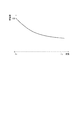
すなわち、本実施形態では、上述のように、光源部12から出射されるリファレンス光として、面内において光量のばらつきがなく、かつ、分光波長域における各波長成分の光量が一定である光を用いる。また、各受光素子133Aは、分光波長域における各波長成分に対する感度が一定である。更に、白色基準板Xは、分光波長域における各波長成分に対して反射率が一定である。このような構成では、各受光素子133Aにて受光される光は、固定フィルター132の透過率特性に基づいてその光量が決定される。
図9は、本実施形態における各受光素子133Aにおいて、各受光素子から出力される信号値の特性(信号特性)を示す図である。この図9に示すように、本実施形態では、固定フィルター132の透過率特性に応じて、受光素子133Aにて受光される光に対する信号値が定まり、波長取得部165は、この信号値に基づいて受光素子133Aで受光された光の中心波長を特定する。
例えば、図9に示すように、ある受光素子133Aにおいて、信号値Siが出力された場合、その受光素子133Aにおいて受光された光の中心波長はλiであると特定することができる。
In step S4, the
That is, in the present embodiment, as described above, as the reference light emitted from the
FIG. 9 is a diagram illustrating characteristics (signal characteristics) of signal values output from each light receiving element in each light receiving
For example, as shown in FIG. 9, when a signal value Si is output from a certain
以上のようなステップS4の処理は、各受光素子133Aに対し、ステップS3により取得された各信号値に関して実施される。すなわち、ギャップG1の寸法を所定間隔で変化させた際に、各受光素子133Aでどの波長の光が受光されるかを取得する。言い換えれば、波長取得部165は、駆動電圧Vに対する各受光素子133Aでの受光中心波長λを取得する。取得したデータは、各受光素子133AにおけるV−λデータとして、記憶部161に記憶される。
以上のように、各受光素子133Aでの受光中心波長を取得することにより、波長可変干渉フィルター5における反射膜54,55間の面内ばらつきの分布を把握することができる。
The process in step S4 as described above is performed for each signal value acquired in step S3 for each light receiving
As described above, the distribution of in-plane variation between the
(分光画像撮像処理)
次に、本実施形態の分光カメラ1による分光画像の取得方法について説明する。
本実施形態では、上述の受光波長取得処理により、波長可変干渉フィルター5の反射膜54,55間の面内ばらつきの分布を把握することができるため、このような面内ばらつきの分布を考慮した精度の高い分光画像を取得することが可能となる。
(Spectral imaging process)
Next, a method for acquiring a spectral image by the spectral camera 1 of the present embodiment will be described.
In the present embodiment, the distribution of in-plane variation between the
図10は、本実施形態の分光画像撮像処理を示すフローチャートである。図11は、分光画像を撮像する際の各光学部材の配置、及び測定光の進路を示す図である。
分光画像撮像処理では、まず、フィルター移動制御部164は、進退機構132Aを制御し、固定フィルター132を入射光学系131の光路上から退避させる(ステップS11)。
また、光源制御部163は、光源部12を駆動させ、撮像対象に対して光(リファレンス光)を照射する(ステップS12)。本実施形態では、リファレンス光は分光波長域の各波長成分の光量が略同じとなるため、リファレンス光の照射によって、撮像対象から特定の波長の光の光量のみが変化することがなく、撮像部133における受光量の向上を図れる。
ステップS11及びステップS12により、図11に示すように、撮像対象で反射された光は、入射光学系131から波長可変干渉フィルター5に導かれ、波長可変干渉フィルター5を透過した光が撮像部133にて受光される。
FIG. 10 is a flowchart showing the spectral image capturing process of the present embodiment. FIG. 11 is a diagram illustrating the arrangement of optical members and the path of measurement light when a spectral image is captured.
In the spectral image capturing process, first, the filter
In addition, the light
As shown in FIG. 11, the light reflected by the imaging target in steps S <b> 11 and S <b> 12 is guided from the incident
この後、ユーザーにより分光画像を撮像する旨の操作が実施されると、測定制御部166は、フィルター駆動回路134から静電アクチュエーター56に印加する駆動電圧を順次変化させて、反射膜54,55間のギャップG1の寸法を例えば一定間隔で変化させ、駆動電圧を順次変化させた際の各受光素子133Aから出力される信号値を取得する。つまり、ギャップG1を走査させた際の各受光素子133Aから出力される信号値を取得する(ステップS13)。なお、設定される各駆動電圧としては、上記ステップS3における駆動電圧と同じ電圧値にすることが好ましい。
ここで、静電アクチュエーター56に印加する駆動電圧に対して、各受光素子133Aで受光される光の中心波長は、上記受光波長取得処理により取得されている。つまり、ステップS13において静電アクチュエーター56に印加された駆動電圧に対する各受光素子133Aで受光される光の中心波長は既知となる。
よって、分光画像撮像処理では、各受光素子133Aにおいて受光される光の中心波長と、その光量を取得することができる。
Thereafter, when an operation for capturing a spectral image is performed by the user, the
Here, with respect to the drive voltage applied to the electrostatic actuator 56, the center wavelength of the light received by each light receiving
Therefore, in the spectral image capturing process, it is possible to acquire the center wavelength of the light received by each light receiving
この後、スペクトル測定部167は、反射膜54,55間のギャップG1の寸法を順次変更した際の各受光素子133Aにおける受光量(各画素の光量)と、その受光中心波長とに基づいて、各画素の分光スペクトルを測定する(ステップS14)。
次に、画像処理部168は、分光画像の生成対象となる目標波長を取得する(ステップS15)。この目標波長の取得としては、例えば、画像処理部168は、ユーザーによる操作部15の操作により、目標波長を取得してもよく、目標波長が予め設定されていてもよい。目標波長の数としては特に限定されない。
そして、画像処理部168は、各画素の分光スペクトルから設定された目標波長に対する光量を取得し(ステップS16)、当該光量を画素値とした分光画像を生成する(ステップS17)。
以上により、目標波長の分光画像が生成される。
Thereafter, the
Next, the
Then, the
Thus, a spectral image of the target wavelength is generated.
[本実施形態の作用効果]
本実施形態の分光カメラ1では、受光波長取得処理において、光源部12からリファレンス光を出射させ、このリファレンス光を基準板Xで反射させ、波長可変干渉フィルター5を介して撮像部133に入射した光を検出する。この際、リファレンス光の各波長成分の光をそれぞれ個別に各受光素子133Aで受光させた際に、図9に示すように、各波長成分に対する信号値がそれぞれ異なる値となる。そして、波長取得部165は、撮像部133の各受光素子133Aから出力される信号値に基づいて、当該各受光素子133Aでの受光中心波長を取得する。
このような構成では、受光波長取得処理において、リファレンス光を受光した際の信号値に基づいて、容易かつ精度よく、各受光素子133Aで受光された光の中心波長を特定することができる。従って、分光画像取得処理において、撮像画像を撮像した際に、撮像画像における各画素がどの波長に対応した画素値であるかを容易に判定することができ、目標波長に対する分光画像を精度よく取得することができる。例えば、各受光素子133Aで目標波長の光を受光されるように、波長可変干渉フィルター5のギャップG1の寸法を順次変化させてその信号値を取得し、これらの信号値に基づいて、全画素が目標波長の光量に対応した階調値となる分光画像を生成する等により、高精度な分光画像を取得することができる。
[Operational effects of this embodiment]
In the spectral camera 1 of the present embodiment, in the received light wavelength acquisition process, the reference light is emitted from the
In such a configuration, the center wavelength of the light received by each light receiving
本実施形態では、入射光学系131から入射された光が撮像部133に到達するまでの間の光路上に、分光波長域の各波長成分に対する透過率がそれぞれ異なる固定フィルター132が進退自在に設けられている。
分光波長域において、リファレンス光の各波長成分における光量が一定(又は略一定)であり、各受光素子133Aの各波長成分に対する感度が一定(又は略一定)である場合、リファレンス光を各受光素子133Aで受光した場合に、受光中心波長を判定することが困難となる。これに対して、本実施形態では、透過率特性が各波長で異なる固定フィルター132を用いることで、各受光素子133Aから出力される信号値が各波長成分でそれぞれ異なる値となり、受光中心波長の特定が容易にできる。
In the present embodiment, a fixed
When the light quantity in each wavelength component of the reference light is constant (or substantially constant) in the spectral wavelength range, and the sensitivity to each wavelength component of each light receiving
本実施形態では、リファレンス光を受光素子で受光した際の信号特性が、図9に示すように、波長増加方向に対して単調減少する。このように、波長に対して信号値が単調変化する場合、信号値に対して対応する波長が1つに決まることになるので、より精度よく受光素子133Aでの受光中心波長を特定することができる。
そして、このような信号特性を得るために、本実施形態では、固定フィルター132として、ガラス基板にAg及びAl2O3を積層させたフィルターを用いる。このような固定フィルター132では、簡単な構成で、上記のような信号特性が得られるフィルターを製造できる。
In the present embodiment, as shown in FIG. 9, the signal characteristics when the reference light is received by the light receiving element monotonously decrease with respect to the wavelength increasing direction. As described above, when the signal value monotonously changes with respect to the wavelength, the wavelength corresponding to the signal value is determined as one, so that it is possible to specify the light receiving center wavelength in the
In order to obtain such signal characteristics, in the present embodiment, a filter in which Ag and Al 2 O 3 are laminated on a glass substrate is used as the fixed
本実施形態では、波長可変干渉フィルター5の静電アクチュエーター56に印加する駆動電圧を順次切り替えて、各受光素子133Aでの受光量を検出し、スペクトル測定部167は、これらの受光量に基づいて、撮像画像の各画素における分光スペクトルを測定する。
本実施形態では、受光波長取得処理により、所定の駆動電圧を印加した際の各受光素子133Aで受光される光の波長が取得されている。このため、分光画像取得処理では、ギャップG1の寸法を走査させた際に各受光素子133Aで受光される光の波長とその光量とを正確に取得することができる。これにより、スペクトル測定部167は、各画素における正確な分光スペクトルを測定することができる。
In the present embodiment, the drive voltage applied to the electrostatic actuator 56 of the wavelength
In the present embodiment, the wavelength of light received by each light receiving
本実施形態では、画像処理部168は、スペクトル測定部167により測定された各画素の分光スペクトルから目標波長に対する光量を取得し、取得した光量をその画素の光量とした分光画像を生成する。
この場合、取得した分光画像が複数ある場合(目標波長が複数ある場合)や、撮像操作の後に目標波長を設定する場合において、撮像操作を繰り返す必要がなく、容易に所望の目標波長の分光画像を取得できる。
In the present embodiment, the
In this case, when there are a plurality of acquired spectral images (when there are a plurality of target wavelengths) or when a target wavelength is set after the imaging operation, it is not necessary to repeat the imaging operation, and a spectral image of a desired target wavelength can be easily obtained. Can be obtained.
本実施形態では、光源部12は、面内において光量が均一で、かつ、分光波長域における各波長の光量が同じであるリファレンス光を出射させる。このような構成では、撮像対象の分光画像を撮像する際に、リファレンス光を用いることができる。例えば自然光等の外光を撮像対象への照射光として用いる場合、波長によって光量が異なることが考えられ、この場合、外光の影響により撮像対象の正確な分光画像が得られない場合がある。例えば、分光画像に基づいて成分分析等を実施する場合には、特に、その影響が大きくなる。これに対して、本実施形態では、上記のようなリファレンス光を用いることで、照射光の波長によるばらつきがなく、正確な分光画像を取得することができる。
In the present embodiment, the
本実施形態では、ステップS3において、波長可変干渉フィルター5の静電アクチュエーター56に印加する駆動電圧を順次変化させて、その都度、受光素子133Aから出力される信号値を取得する。そして、波長取得部165は、これらの信号値に基づいて、静電アクチュエーター56に印加する駆動電圧に対する各受光素子133Aでの受光中心波長を取得する。
このような構成では、ギャップG1の寸法変動によって、可動基板52の撓み状態が変化し、反射膜54,55間のギャップG1の面内ばらつきが変化する場合でも、各ギャップ寸法に対する受光素子133Aでの受光中心波長を取得することができる。これにより、基板撓みによる面内ばらつきの分布をも把握することができ、分光画像取得処理において、より精度の高い分光画像を取得することができる。
In this embodiment, in step S3, the drive voltage applied to the electrostatic actuator 56 of the wavelength
In such a configuration, even when the bending state of the
また、本実施形態では、波長取得部165により取得された受光素子133Aでの受光波長は、上述のような波長可変干渉フィルター5におけるギャップG1の面内ばらつきのみではなく、入射光学系131により導かれた光の波長可変干渉フィルター5への入射角をも考慮された受光波長となる。すなわち、波長可変干渉フィルター5は、反射膜54,55に入射する光の入射角が変化すると、反射膜54,55間での光学距離が変動するため、透過光の波長も変動する。本実施形態では、ギャップG1の面内ばらつきに加え、上記のような入射光の入射位置による入射角のばらつきによって、波長可変干渉フィルター5の透過光の波長がずれた場合でも、各受光素子133Aでの受光中心波長を精度よく取得することができる。すなわち、本実施形態では、波長可変干渉フィルター5の製造上の面内ばらつきや、入射光学系131の製造上のばらつきがある場合でも、精度の高い分光画像を取得することができる。
Further, in the present embodiment, the light reception wavelength at the
[第二実施形態]
次に、本発明に係る第二実施形態について説明する。
上記第一実施形態では、リファレンス光の波長特性、受光素子133Aの感度特性、及び白色基準板Xの反射率特性が、分光波長域における各波長成分で略一定である例を示した。
これに対して、本実施形態では、リファレンス光の波長特性が、分光波長域の各波長成分で異なる点で上記第一実施形態と相違する。なお、以降の説明に当たり、第一実施形態と同様の構成や処理ステップについては、同符号を付し、その説明を省略又は簡略化する。
[Second Embodiment]
Next, a second embodiment according to the present invention will be described.
In the first embodiment, an example is shown in which the wavelength characteristics of the reference light, the sensitivity characteristics of the
On the other hand, this embodiment is different from the first embodiment in that the wavelength characteristic of the reference light is different for each wavelength component in the spectral wavelength range. In the following description, the same configurations and processing steps as those in the first embodiment are denoted by the same reference numerals, and the description thereof is omitted or simplified.
図12は、第二実施形態の光源部から出力されるリファレンス光の波長特性を示す図である。図13は、第二実施形態の固定フィルター132の透過率特性を示す図である。
図12に示すように、本実施形態では、光源部12から出力されるリファレンス光は、分光波長域の各波長成分でそれぞれ異なる値となる。この場合では、固定フィルター132として、例えば、図13に示すような透過率特性を有するフィルターを用いる。
これにより、リファレンス光を受光素子133Aで受光した際に、図9に示すように、波長増加方向に対して、信号値が単調減少する信号特性を得ることができる。
このような構成でも、上記第一実施形態と同様の処理により、各受光素子133Aにて受光させる光の中心波長を取得することができる。
FIG. 12 is a diagram illustrating the wavelength characteristics of reference light output from the light source unit of the second embodiment. FIG. 13 is a diagram showing the transmittance characteristics of the fixed
As shown in FIG. 12, in this embodiment, the reference light output from the
Thereby, when the reference light is received by the
Even with such a configuration, the center wavelength of the light received by each light receiving
[第三実施形態]
次に、本発明に係る第三実施形態について説明する。
上記第一実施形態では、リファレンス光の波長特性、受光素子133Aの感度特性、及び白色基準板Xの反射率特性が、分光波長域における各波長成分で略一定である例を示した。
これに対して、本実施形態では、受光素子133Aの感度特性が、分光波長域の各波長成分で異なる点で上記第一実施形態と相違する。
[Third embodiment]
Next, a third embodiment according to the present invention will be described.
In the first embodiment, an example is shown in which the wavelength characteristics of the reference light, the sensitivity characteristics of the
On the other hand, this embodiment is different from the first embodiment in that the sensitivity characteristic of the
図14は、第三実施形態の受光素子133Aにおける感度特性を示す図である。図15は、第三実施形態の固定フィルター132の透過率特性を示す図である。
図14に示すように、本実施形態では、受光素子133Aの感度特性は、分光波長域の各波長成分でそれぞれ異なる値となる。この場合では、固定フィルター132として、例えば、図15に示すような透過率特性を有するフィルターを用いる。
これにより、リファレンス光を受光素子133Aで受光した際に、図9に示すように、波長増加方向に対して、信号値が単調減少する信号特性を得ることができる。
このような構成でも、上記第一実施形態と同様の処理により、各受光素子133Aにて受光させる光の中心波長を取得することができる。
FIG. 14 is a diagram showing sensitivity characteristics in the
As shown in FIG. 14, in this embodiment, the sensitivity characteristics of the
Thereby, when the reference light is received by the
Even with such a configuration, the center wavelength of the light received by each light receiving
[第四実施形態]
次に本発明の第四実施形態について図面に基づいて説明する。
上記第一実施形態では、分光画像取得装置である分光カメラ1において、各受光素子133Aでの受光中心波長を取得し、当該受光波長に基づいて、精度の高い分光画像を取得する例を示したが、本発明の構成を用いることで、受光素子133Aに入射する入射角を求めることもできる。受光素子133Aへの光入射角は、波長可変干渉フィルター5への入射角であり、この入射角のばらつきを検査することにより、入射光学系131を構成する各レンズの歪み等を検査することも可能となる。
第四実施形態では、上記のような受光素子133Aへの光の入射角を求める構成及び入射角取得方法について、説明する。
なお、本実施形態では、入射光学系131を構成する各レンズの歪み等を検査することを目的とするものであり、波長可変干渉フィルター5として、面内ムラがないフィルターを用いることが好ましい。このようなフィルターとして、保持部522(ダイアフラム)が設けられていない波長可変干渉フィルターを用いてもよい。この場合、保持部522の撓みに起因する反射膜間のギャップG1における面内ムラが抑制される。また、波長可変干渉フィルター5に限られず、例えばギャップG1が固定された干渉フィルターを用いてもよい。この場合では、例えば、反射膜間に光学膜を配置した、エアギャップが設けられない干渉フィルター等を用いることができる。
[Fourth embodiment]
Next, a fourth embodiment of the present invention will be described with reference to the drawings.
In the first embodiment, in the spectroscopic camera 1 that is a spectroscopic image acquisition device, an example is shown in which the light receiving center wavelength at each light receiving
In the fourth embodiment, a configuration for obtaining an incident angle of light to the
In this embodiment, the objective is to inspect the distortion or the like of each lens constituting the incident
図16は、本実施形態における分光カメラ1の概略構成を示す図であり、制御部16の処理部162は、上記第一実施形態の各機能構成に加え、本発明の入射角取得部169としても機能する。
図17は、入射角取得処理を示すフローチャートである。
図18及び図19は、本実施形態における受光素子133Aへの入射角取得方法を説明するための図である。
第四実施形態における入射角取得処理では、まず、入射光学系131を、リファレンス光の光路から退避させる(ステップS21)。入射光学系131は、分光カメラ1に対して着脱可能な構成としてもよく、製造時の入射角の検査時に一時的に入射光学系131を取り外す等であってもよい。
この後、図18に示すように、分光カメラ1に対して、コヒーレント光を入射させる(ステップS22)。コヒーレント光を入射させることで、全受光素子133Aに対して例えば90°で光が入射する。
次に、波長取得部165は、上記第一実施形態と同様、各受光素子133Aから出力される信号値に基づき、各受光素子133Aでの受光中心波長(第一受光波長)を取得する(ステップS23)。
FIG. 16 is a diagram illustrating a schematic configuration of the spectroscopic camera 1 according to the present embodiment. A
FIG. 17 is a flowchart showing the incident angle acquisition process.
18 and 19 are diagrams for explaining a method of obtaining an incident angle on the
In the incident angle acquisition process in the fourth embodiment, first, the incident
Thereafter, as shown in FIG. 18, coherent light is incident on the spectroscopic camera 1 (step S22). By making the coherent light incident, the light is incident on all the
Next, as in the first embodiment, the
次に、入射光学系131を分光カメラ1にセットする等により、リファレンス光の光路上に配置させる(ステップS24)。本実施形態では、入射光学系131により、図19に示すように、各受光素子133Aに対してそれぞれ異なる入射角で光が入射する。
そして、波長取得部165は、上記第一実施形態と同様、各受光素子133Aから出力される信号値に基づき、各受光素子133Aでの受光中心波長(第二受光波長)を取得する(ステップS25)。
Next, the incident
And the
この後、入射角取得部169は、第一受光波長λ1、第二受光波長λ2、及び波長可変干渉フィルター5におけるギャップG1の初期ギャップ寸法に基づいて、受光素子133Aへの入射角を取得(算出)する(ステップS26)。
図20は、1つの受光素子133Aでの受光波長が変化した際のモデルを示す図である。
図20に示すように、ステップS23で取得された1つの受光素子133Aにおける第一受光波長λ1は、波長可変干渉フィルター5の反射膜54,55の法線方向から入射した光であるため、次数をm、反射膜54,55間の媒体の屈折率をnとして、下記式(1)により表せる。
Thereafter, the incident
FIG. 20 is a diagram illustrating a model when the light receiving wavelength of one
As shown in FIG. 20, the first light receiving wavelength λ 1 in one

上記(1)式において、d1は、反射膜54,55間のギャップG1の初期ギャップ寸法である。第一受光波長λ1に基づいて、初期ギャップ寸法d1を算出することが可能となる。
一方、ステップS25において、波長可変干渉フィルター5の反射膜54,55に対して入射角θで光が入射した場合、受光素子133Aにおける第二受光波長λ2は、下記式(2)となる。
In the above formula (1), d 1 is the initial gap dimension of the gap G 1 between the
On the other hand, when light is incident on the
従って、入射角取得部169は、ステップS23により取得された第一受光波長λ1を式(1)に代入することにより、初期ギャップ寸法d1を算出し、算出された初期ギャップ寸法d1及び、ステップS25により取得された第二受光波長λ2を式(2)に代入することにより、入射角θを算出する。
Therefore, the incident
以上のような第四実施形態では、撮像部133の各受光素子133Aに対して入射する光の入射角θを取得することができる。このような構成では、各受光素子133Aにおける光の入射角θが適切な角であるかを精度よく検査することができる。これにより、入射角θを決定する入射光学系131の各レンズの歪みや収差等を検査することが可能となり、より精度の高い分光画像を撮像可能な分光カメラ1を提供することができる。
In the fourth embodiment as described above, the incident angle θ of the light incident on each light receiving
なお、本実施形態では、上述のように、入射光学系131の各レンズの歪みの検査を目的として、波長可変干渉フィルター5として、面内ムラがない基準フィルター(例えば、保持部522が設けられないフィルターや、エアギャップが設けられていない干渉フィルター)を用いている。この場合、上記により、各レンズに歪みがないことを確認した後、分光カメラ1に波長可変干渉フィルター5を組込み、上記第一から第三実施形態に示す方法を用いて、各受光素子133Aにおいて受光される光の波長を特定してもよい。
In the present embodiment, as described above, for the purpose of inspecting distortion of each lens of the incident
また、第四実施形態では、面内ムラがない波長可変干渉フィルター5や波長固定側の干渉フィルターを用いる例を示したが、これに限定されない。すなわち、ステップS22においてコヒーレント光を入射させ、ステップS23において第一受光波長を取得することで、各受光素子133Aの信号値から波長可変干渉フィルター5の幾何学的な形状(ギャップG1の寸法の面内ムラ)を算出することができる。したがって、光が入射角θで入射した際のギャップdは、入射角θを用いた関数d(θ)により近似することができる。このような方法では、別途基準フィルターを用意する必要がなく、入射光学系を各レンズの歪みを検査することも可能となる。
In the fourth embodiment, the wavelength
[他の実施形態]
なお、本発明は前述の実施形態に限定されるものではなく、本発明の目的を達成できる範囲での変形、改良等は本発明に含まれるものである。
[Other Embodiments]
It should be noted that the present invention is not limited to the above-described embodiments, and modifications, improvements, and the like within the scope that can achieve the object of the present invention are included in the present invention.
上記第一実施形態では、ステップS3において、波長可変干渉フィルター5の静電アクチュエーター56に印加する駆動電圧を順次変化させ、各駆動電圧に対して、各受光素子133Aから出力される信号値を取得した。これに対して、ステップS3において、波長可変干渉フィルター5を駆動させなくてもよい。この場合、反射膜54,55間のギャップG1を初期ギャップ寸法とした状態での、ギャップG1の面内ばらつきを測定することが可能となる。
このような処理は、例えば、波長可変干渉フィルター5の製造において、初期ギャップ寸法の検査等に適用することができる。
また、例えば可動部521の厚み寸法が大きい場合等、ギャップG1が変動した場合でも、可動部521や可動反射膜55に撓みが生じない場合では、上記のように、初期ギャップ寸法のバラつきを検出するだけでもよい。この場合、分光画像撮像処理では、取得された分光画像の各画素値を、初期ギャップ寸法のばらつきに基づいて補正すればよい。
In the first embodiment, in step S3, the drive voltage applied to the electrostatic actuator 56 of the wavelength
Such a process can be applied to, for example, inspection of an initial gap dimension in the manufacture of the variable
Further, even when the gap G1 fluctuates, for example, when the thickness dimension of the
上記第一実施形態では、分光画像撮像処理において、固定フィルター132を光路上から退避させたが、光路上に配置した状態であってもよい。この場合、固定フィルター132の透過率特性が既知であるので、撮像画像の各画素値を、固定フィルター132の透過率特性に基づいて補正すればよい。
In the first embodiment, in the spectral image capturing process, the fixed
また、上記第一実施形態では、分光画像撮像処理において、光源を駆動させて、リファレンス光を照射させる例を示したが、これに限定されない。すなわち、自然光を用いた分光画像撮像処理を実施してもよい。
また、上記第一実施形態では、リファレンス光として分光波長域における各波長成分の光量が一定である例を示したが、リファレンス光の各波長成分の光量がそれぞれ異なり、その波長特性が既知である場合では、撮像画像の各画素値を波長特性に基づいて補正すればよい。
In the first embodiment, the example in which the light source is driven and the reference light is irradiated in the spectral image capturing process has been described. However, the present invention is not limited to this. That is, spectral image capturing processing using natural light may be performed.
In the first embodiment, the example in which the light amount of each wavelength component in the spectral wavelength region is constant as the reference light has been described. However, the light amount of each wavelength component of the reference light is different, and the wavelength characteristics thereof are known. In some cases, each pixel value of the captured image may be corrected based on the wavelength characteristics.
第二実施形態において、リファレンス光の波長特性及び固定フィルターの透過率特性をかけ合せた際に、また、第三実施形態においては、受光素子の感度特性及び固定フィルターの透過率特性をかけ合せた際に、図9に示すような単調変化となる信号特性が得られる構成とした。
これに対して、例えば、リファレンス光の波長特性が、波長増加方向に対して単調変化(単調増加や単調減少)する場合では、固定フィルター132を用いなくてもよい。同様に、受光素子133Aの感度特性が、波長増加方向に対して単調変化(単調増加や単調減少)する場合では、固定フィルター132を用いなくてもよい。また、リファレンス光の波長特性や、受光素子133Aの感度特性が分光波長域の各波長成分で略一定である場合でも、基準板Xの反射率特性が波長増加方向に対して単調変化する場合、固定フィルター132を用いなくてもよい。
すなわち、本発明では、リファレンス光を受光素子133Aで受光した際に、図9に示すような信号特性が得られる構成であれば、いかなる組み合わせの光学部材を用いてもよい。従って、例えば、リファレンス光の波長特性、受光素子133Aの感度特性、及び基準板Xの反射率特性がそれぞれ異なる場合でも、これらの各特性をかけ合せた際に、例えばリファレンス光を受光素子133Aで受光した際に、図9に示すような信号特性の信号値が出力されるように、各部材の素材等を設定すればよく、各部材の素材等を変更できない場合では、図9に示すような信号特性が得られるように固定フィルター132を設計すればよい。
In the second embodiment, when the wavelength characteristic of the reference light and the transmittance characteristic of the fixed filter are multiplied, and in the third embodiment, the sensitivity characteristic of the light receiving element and the transmittance characteristic of the fixed filter are multiplied. In this case, a signal characteristic having a monotonous change as shown in FIG. 9 is obtained.
On the other hand, for example, when the wavelength characteristic of the reference light monotonously changes (monotonically increases or monotonously decreases) in the wavelength increasing direction, the fixed
That is, in the present invention, any combination of optical members may be used as long as the signal characteristics as shown in FIG. 9 are obtained when the reference light is received by the
上記第一実施形態では、光源部12が分光カメラ1に一体的に設けられる構成を示したが、これに限定されず、リファレンス光を出射する光源が分光カメラ1に対して別体で設けられてもよい。この場合では、光源部12からのリファレンス光を、基準板Xを介さずに、直接入射光学系131に入射させてもよい。
In the first embodiment, the configuration in which the
上記第一実施形態において、スペクトル測定部167により撮像画像の各画素における分光スペクトルを測定し、画像処理部168は、その分光スペクトルに基づいて、目標波長の光量を取得して分光画像を生成する例を示したが、これに限定されない。
例えば、分光画像として取得した目標波長が予め設定されている場合では、測定制御部166により、各受光素子133Aで目標波長を取得可能なギャップG1となるように、順次駆動電圧を切り替えて、受光素子133Aからの信号値を取得する。そして、画像処理部168は、受光素子133Aでの受光波長が目標波長となった際の信号値に基づいて分光画像を生成する。
つまり、受光素子Aでは、駆動電圧Vaの際の受光波長が目標波長λsとなり、受光素子Bでは、駆動電圧Vbの際の受光波長が目標波長λsとなる場合、測定制御部166は、静電アクチュエーター56に印加する駆動電圧をVa,Vbに順次切り替える。そして、画像処理部168は、駆動電圧Vaの際の受光素子Aからの信号値を、受光素子Aに対応する画素の画素値とし、駆動電圧Vbの際の受光素子Bからの信号値を、受光素子Bに対応する画素の画素値とした分光画像を生成する。
上記のような分光画像取得処理では、分光スペクトルを測定する処理が不要となり、処理の高速化を図ることができる。
In the first embodiment, the
For example, when the target wavelength acquired as a spectroscopic image is set in advance, the
That is, in the light receiving element A, when the light receiving wavelength at the driving voltage Va is the target wavelength λs, and in the light receiving element B, the light receiving wavelength at the driving voltage Vb is the target wavelength λs, the
In the spectral image acquisition process as described above, the process of measuring the spectral spectrum is unnecessary, and the processing speed can be increased.
上記第一実施形態において、分光カメラ1の内部に波長可変干渉フィルター5が内蔵される構成を例示したが、これに限定されない。例えば、図21に示すように、スマートフォン等のカメラ付き機器に対して、波長可変干渉フィルター5を有するフィルター機構20を装着する構成などとしてもよい。
この場合、図21に示すように、波長可変干渉フィルター5の前段にテレセントリック光学系等の入射光学系を設けない構成としてもよい。この場合、波長可変干渉フィルター5に入射する光は、反射膜54,55に対して垂直に入射されない。しかしながら、上述のように、本発明では、各受光素子133Aに入射される光の中心波長を取得することができるため、受光された光の光量と、その受光波長とを対応付けることで、分光画像を取得することが可能となる。
In the first embodiment, the configuration in which the wavelength
In this case, as shown in FIG. 21, an incident optical system such as a telecentric optical system may not be provided upstream of the wavelength
上記各実施形態において、分光フィルターとして、波長可変干渉フィルター5を例示したが、これに限定されない。分光フィルターとしては、面分光が可能なフィルターであれば、いかなるフィルターを用いてもよく、例えばAOTF(Acousto-Optic Tunable Filter)やLCTF(Liquid crystal tunable filters)等を用いてもよい。
また、波長可変干渉フィルター5として、ギャップG1の寸法に応じた光を透過させる光透過型のエタロン素子を例示したが、これに限定されず、ギャップG1の寸法に応じた光を反射させる光反射型のエタロン素子を用いてもよい。
In each said embodiment, although the wavelength
Moreover, although the light transmission type etalon element which transmits the light according to the size of the gap G1 is illustrated as the wavelength
その他、本発明の実施の際の具体的な構造は、本発明の目的を達成できる範囲で他の構造等に適宜変更できる。 In addition, the specific structure for carrying out the present invention can be appropriately changed to other structures and the like within a range in which the object of the present invention can be achieved.
1…分光カメラ(分光画像取得装置)、5…波長可変干渉フィルター(分光フィルター0)、12…光源部、13…撮像モジュール、16…制御部、20…フィルター機構、54…固定反射膜、55…可動反射膜、56…静電アクチュエーター、131…入射光学系、132…固定フィルター、132A…進退機構、133…撮像部、133A…受光素子、134…フィルター駆動回路、161…記憶部、162…処理部、163…光源制御部、164…フィルター移動制御部、165…波長取得部、166…測定制御部、167…スペクトル測定部、168…画像処理部、169…入射角取得部、G1…ギャップ、X…基準板。 DESCRIPTION OF SYMBOLS 1 ... Spectroscopic camera (spectral image acquisition apparatus), 5 ... Wavelength variable interference filter (spectral filter 0), 12 ... Light source part, 13 ... Imaging module, 16 ... Control part, 20 ... Filter mechanism, 54 ... Fixed reflection film, 55 DESCRIPTION OF SYMBOLS ... Movable reflective film, 56 ... Electrostatic actuator, 131 ... Incident optical system, 132 ... Fixed filter, 132A ... Advance / retract mechanism, 133 ... Imaging unit, 133A ... Light receiving element, 134 ... Filter drive circuit, 161 ... Storage unit, 162 ... Processing unit 163: Light source control unit, 164: Filter movement control unit, 165 ... Wavelength acquisition unit, 166 ... Measurement control unit, 167 ... Spectrum measurement unit, 168 ... Image processing unit, 169 ... Incident angle acquisition unit, G1 ... Gap , X: Reference plate.
Claims (12)
複数の受光素子を有し、前記分光フィルターにより分光された光を受光する撮像部と、
リファレンス光を前記撮像部で受光した際に、前記複数の受光素子の各々から出力される信号値に基づいて、前記複数の受光素子の各々に入射した光の中心波長を取得する波長取得部と、を備え、
前記リファレンス光に含まれる所定波長域における複数の波長成分の各々の光量は、前記リファレンス光の光軸に対して交差する面内において略均一であり、
前記リファレンス光の前記所定波長域における複数の波長成分の各々の光を前記撮像部で受光させた際に前記受光素子から出力される信号値は、波長成分毎に異なり、
前記波長取得部は、前記撮像部で前記リファレンス光を受光した際に、前記複数の受光素子のそれぞれから出力される、前記一対の反射膜のギャップ寸法の変化に応じた信号値に基づいて、前記複数の受光素子の各々に入射した光の中心波長を取得する
ことを特徴とする分光画像取得装置。 A spectroscopic filter having a pair of reflective films and spectrally separating incident light;
An imaging unit having a plurality of light receiving elements and receiving the light separated by the spectral filter;
A wavelength acquisition unit that acquires a center wavelength of light incident on each of the plurality of light receiving elements based on a signal value output from each of the plurality of light receiving elements when a reference light is received by the imaging unit; With
Amount of each of the plurality of wavelength components in a predetermined wavelength band included in the reference light is substantially uniform in a plane intersecting the optical axis of the reference light,
Signal value output from the light receiving element when obtained by receiving light of each of the plurality of wavelength components in the predetermined wavelength range of the reference light by the imaging unit, varies for each wavelength component,
The wavelength acquisition unit is output from each of the plurality of light receiving elements when the reference light is received by the imaging unit, based on a signal value according to a change in the gap dimension of the pair of reflective films, A spectral image acquisition apparatus that acquires a center wavelength of light incident on each of the plurality of light receiving elements .
前記撮像部に入射される光の光路上に配置される固定フィルターを備え、
前記固定フィルターは、前記所定波長域における前記複数の波長成分の各々に対して、異なる透過率を有する
ことを特徴とする分光画像取得装置。 In the spectral image acquisition device according to claim 1,
A fixed filter disposed on an optical path of light incident on the imaging unit;
The spectral filter according to claim 1, wherein the fixed filter has a different transmittance with respect to each of the plurality of wavelength components in the predetermined wavelength region.
前記リファレンス光を出射する光源を有し、
前記光源は、前記所定波長域における前記複数の波長成分の各々に対して、異なる光量の光を出射する
ことを特徴とする分光画像取得装置。 In the spectral image acquisition device according to claim 1,
A light source that emits the reference light;
The spectral light source device, wherein the light source emits light having a different light amount with respect to each of the plurality of wavelength components in the predetermined wavelength region.
前記撮像部における前記複数の受光素子の各々は、前記波長成分毎に異なる感度を有する
ことを特徴とする分光画像取得装置。 In the spectral image acquisition device according to claim 1,
Each of the plurality of light receiving elements in the imaging unit has a different sensitivity for each wavelength component.
前記リファレンス光の前記所定波長域における前記複数の波長成分の各々を前記撮像部で受光させた際に前記受光素子から出力される信号値は、波長に対して単調変化する
ことを特徴とする分光画像取得装置。 In the spectral image acquisition device according to claim 1,
The signal value output from the light receiving element when each of the plurality of wavelength components in the predetermined wavelength range of the reference light is received by the imaging unit changes monotonously with respect to the wavelength. Image acquisition device.
前記撮像部に入射される光の光路上に配置される固定フィルターを備え、
前記固定フィルターは、ガラス基板にAg及びAl2O3を積層させたフィルターである
ことを特徴とする分光画像取得装置。 The spectral image acquisition apparatus according to claim 5,
A fixed filter disposed on an optical path of light incident on the imaging unit;
The fixed filter, spectral image obtainment apparatus, characterized in that the filter as a laminate of Ag and Al 2 O 3 in the glass substrate.
前記分光フィルターは、出射させる光の波長を変更可能であり、
前記分光画像取得装置は、さらに、
前記分光フィルターが分光する光の波長を変化させる測定制御部と、
前記複数の受光素子の各々で受光された同一波長の光の光量に基づいて、当該同一波長に対する分光画像を生成する画像生成部と、
を備えていることを特徴とする分光画像取得装置。 In the spectral image acquisition device according to claim 1,
The spectral filter can change the wavelength of light to be emitted,
The spectral image acquisition device further includes:
A measurement control unit that changes the wavelength of light that the spectral filter splits;
Said plurality of based on the amount of light of the same wavelength of light received by each light receiving element, and an image generating unit that generates a spectral image for those of identity-wave,
A spectral image acquisition apparatus comprising:
前記複数の受光素子の各々で受光される光の分光スペクトルを測定するスペクトル測定部を備えている
ことを特徴とする分光画像取得装置。 In the spectral image acquisition device according to claim 7,
A spectral image acquisition device comprising: a spectrum measuring unit that measures a spectral spectrum of light received by each of the plurality of light receiving elements.
前記画像生成部は、前記複数の受光素子の各々で受光される光の分光スペクトルに基づいて、前記複数の受光素子の各々にて受光された前記同一波長の光に対する光量を取得し、当該同一波長に対する分光画像を生成する
ことを特徴とする分光画像取得装置。 The spectral image acquisition device according to claim 8,
The image generating unit on the basis of the spectrum of light received by each of the plurality of light receiving elements to obtain the light amount for the light of the previous SL same wavelength of light received by each of the plurality of light receiving elements, spectroscopic image acquisition apparatus and generates a spectral image for those of identity-wave.
前記波長取得部により取得された前記複数の受光素子の各々で受光された光の中心波長に基づいて、前記複数の受光素子の各々に入射する光の入射角を取得する入射角取得部を備えている
ことを特徴とする分光画像取得装置。 In the spectral image acquisition device according to claim 1,
An incident angle acquisition unit that acquires an incident angle of light incident on each of the plurality of light receiving elements based on a center wavelength of light received by each of the plurality of light receiving elements acquired by the wavelength acquisition unit. A spectral image acquisition device characterized by comprising:
前記分光フィルターは、互いに対向する一対の反射膜、及び前記一対の反射膜間のギャップ寸法を変更するギャップ変更部を有する波長可変干渉フィルターである
ことを特徴とする分光画像取得装置。 In the spectral image acquisition device according to claim 1,
The spectral image acquisition device, wherein the spectral filter is a wavelength variable interference filter having a pair of reflective films facing each other and a gap changing unit that changes a gap dimension between the pair of reflective films.
リファレンス光を、前記分光フィルターを介して前記撮像部に受光させる第一ステップと、
前記撮像部で受光した際に前記複数の受光素子の各々から出力される信号値に基づいて、前記複数の受光素子の各々に入射した光の中心波長を取得する第二ステップと、を含み、
前記リファレンス光に含まれる所定波長域における複数の波長成分の各々の光量が前記リファレンス光の光軸に対して交差する面内において略均一であり、
前記分光フィルターを介して前記リファレンス光の前記所定波長域における前記複数の波長成分の各々の光を前記撮像部で受光させた際に前記受光素子から出力される信号値は、波長成分毎で異なり、
前記第二ステップでは、前記撮像部で前記リファレンス光を受光した際に、前記複数の受光素子のそれぞれから出力される、前記一対の反射膜のギャップ寸法の変化に応じた信号値に基づいて、前記複数の受光素子の各々に入射した光の中心波長を取得する
ことを特徴とする受光波長取得方法。 Receiving wavelength acquisition in a spectral image acquisition device having a spectral filter that has a pair of reflective films and that splits incident light, and an imaging unit that has a plurality of light receiving elements and receives light split by the spectral filter A method,
A first step of causing the imaging unit to receive reference light through the spectral filter;
A second step of obtaining a center wavelength of light incident on each of the plurality of light receiving elements based on a signal value output from each of the plurality of light receiving elements when received by the imaging unit,
The amount of each of a plurality of wavelength components in a predetermined wavelength range included in the reference light is substantially uniform in a plane intersecting the optical axis of the reference light,
A signal value output from the light receiving element when the light of each of the plurality of wavelength components in the predetermined wavelength range of the reference light is received by the imaging unit via the spectral filter is different for each wavelength component. The
In the second step, when the reference light is received by the imaging unit, based on a signal value corresponding to a change in the gap size of the pair of reflective films that is output from each of the plurality of light receiving elements, A method for obtaining a received light wavelength, comprising: obtaining a center wavelength of light incident on each of the plurality of light receiving elements .
Priority Applications (3)
| Application Number | Priority Date | Filing Date | Title |
|---|---|---|---|
| JP2014156542A JP6467801B2 (en) | 2014-07-31 | 2014-07-31 | Spectral image acquisition device and received light wavelength acquisition method |
| US14/813,472 US9857221B2 (en) | 2014-07-31 | 2015-07-30 | Spectral image acquisition apparatus and light reception wavelength acquisition method |
| CN201510463692.8A CN105323443B (en) | 2014-07-31 | 2015-07-31 | Spectral image acquisition device and by optical wavelength adquisitiones |
Applications Claiming Priority (1)
| Application Number | Priority Date | Filing Date | Title |
|---|---|---|---|
| JP2014156542A JP6467801B2 (en) | 2014-07-31 | 2014-07-31 | Spectral image acquisition device and received light wavelength acquisition method |
Publications (3)
| Publication Number | Publication Date |
|---|---|
| JP2016033489A JP2016033489A (en) | 2016-03-10 |
| JP2016033489A5 JP2016033489A5 (en) | 2017-08-31 |
| JP6467801B2 true JP6467801B2 (en) | 2019-02-13 |
Family
ID=55181434
Family Applications (1)
| Application Number | Title | Priority Date | Filing Date |
|---|---|---|---|
| JP2014156542A Active JP6467801B2 (en) | 2014-07-31 | 2014-07-31 | Spectral image acquisition device and received light wavelength acquisition method |
Country Status (3)
| Country | Link |
|---|---|
| US (1) | US9857221B2 (en) |
| JP (1) | JP6467801B2 (en) |
| CN (1) | CN105323443B (en) |
Families Citing this family (8)
| Publication number | Priority date | Publication date | Assignee | Title |
|---|---|---|---|---|
| EP3577062A1 (en) * | 2017-02-03 | 2019-12-11 | Gamaya SA | Wide-angle computational imaging spectroscopy method and apparatus |
| WO2018155289A1 (en) * | 2017-02-24 | 2018-08-30 | パナソニックIpマネジメント株式会社 | Dryness sensor |
| US10955336B2 (en) * | 2017-08-26 | 2021-03-23 | Innovative Micro Technology | Gas sensor comprising a rotatable Fabry-Perot multilayer etalon |
| JP7196640B2 (en) * | 2019-01-29 | 2022-12-27 | セイコーエプソン株式会社 | Information system and identification method |
| JP7318215B2 (en) * | 2019-01-30 | 2023-08-01 | セイコーエプソン株式会社 | Image projection system and projection position detection method |
| CN111936907B (en) * | 2019-09-04 | 2021-11-23 | 深圳市海谱纳米光学科技有限公司 | Optical lens and optical equipment |
| CN111323124B (en) * | 2020-04-02 | 2024-02-20 | 江苏双利合谱科技有限公司 | Broadband hyperspectral camera with mounting structure and film coating method thereof |
| JP2021192002A (en) * | 2020-06-05 | 2021-12-16 | セイコーエプソン株式会社 | Image generation device and image generation method |
Family Cites Families (30)
| Publication number | Priority date | Publication date | Assignee | Title |
|---|---|---|---|---|
| JPH04125429A (en) | 1990-09-17 | 1992-04-24 | Hitachi Ltd | Apparatus for monitoring plane spectroscopy |
| US5225888A (en) * | 1990-12-26 | 1993-07-06 | International Business Machines Corporation | Plasma constituent analysis by interferometric techniques |
| JPH11304588A (en) | 1998-04-23 | 1999-11-05 | Hochiki Corp | Narrow-band filter device |
| JP2000039360A (en) | 1998-07-22 | 2000-02-08 | Mitsubishi Electric Corp | Light spectrum-measuring apparatus |
| JP2005195474A (en) | 2004-01-07 | 2005-07-21 | Nec Corp | Multiple-wavelength batch monitoring method and device |
| NO322438B1 (en) | 2005-04-15 | 2006-10-02 | Sinvent As | Adjustable interference filter |
| JP5082648B2 (en) | 2007-07-24 | 2012-11-28 | カシオ計算機株式会社 | IMAGING DEVICE, IMAGING DEVICE CONTROL PROGRAM, AND IMAGING DEVICE CONTROL METHOD |
| US8063976B2 (en) | 2007-07-24 | 2011-11-22 | Casio Computer Co., Ltd. | Image pick-up apparatus and method of controlling the image pick-up apparatus |
| JP2009168597A (en) | 2008-01-16 | 2009-07-30 | Hoya Corp | Spectroscopic instrument, electronic endoscope and electronic endoscope system |
| US20100296099A1 (en) * | 2008-02-06 | 2010-11-25 | Van Brocklin Andrew L | Optical device |
| JP2010032867A (en) * | 2008-07-30 | 2010-02-12 | Enplas Corp | Infrared ray cutoff filter |
| FR2934805A1 (en) * | 2008-08-07 | 2010-02-12 | Inergy Automotive Systems Res | METHOD FOR ATTACHING AN ACCESSORY TO A HOLLOW BODY OF PLASTIC MATERIAL DURING MOLDING |
| JP2010286291A (en) | 2009-06-10 | 2010-12-24 | Hioki Ee Corp | Infrared spectroscope and infrared spectral measuring device |
| JP5617523B2 (en) * | 2009-12-08 | 2014-11-05 | 株式会社村田製作所 | Manufacturing method of multilayer piezoelectric thin film filter |
| JP5531832B2 (en) * | 2010-07-06 | 2014-06-25 | セイコーエプソン株式会社 | Optical filter, optical filter module, spectrophotometer and optical instrument |
| JP2012063239A (en) | 2010-09-16 | 2012-03-29 | Hioki Ee Corp | Infrared spectrophotometry apparatus |
| JP5609542B2 (en) * | 2010-10-28 | 2014-10-22 | セイコーエプソン株式会社 | Light measuring device |
| JP5810512B2 (en) * | 2010-11-12 | 2015-11-11 | セイコーエプソン株式会社 | Optical device |
| JP5720200B2 (en) * | 2010-11-25 | 2015-05-20 | セイコーエプソン株式会社 | Optical module and optical measuring device |
| JP5601190B2 (en) | 2010-12-17 | 2014-10-08 | 株式会社デンソー | Wavelength selective infrared detector |
| WO2012098599A1 (en) * | 2011-01-17 | 2012-07-26 | パナソニック株式会社 | Imaging device |
| JP5879745B2 (en) * | 2011-05-20 | 2016-03-08 | セイコーエプソン株式会社 | Spectral estimation parameter generation apparatus and method, and computer program |
| JP5879893B2 (en) | 2011-10-06 | 2016-03-08 | セイコーエプソン株式会社 | Optical filter device, optical module and electronic equipment |
| JP2013088263A (en) * | 2011-10-17 | 2013-05-13 | Sumitomo Electric Ind Ltd | Spectroscopic instrument calibration method |
| JP5786672B2 (en) | 2011-11-18 | 2015-09-30 | セイコーエプソン株式会社 | Spectrometer |
| JP6216491B2 (en) | 2012-02-20 | 2017-10-18 | セイコーエプソン株式会社 | Spectrometer |
| JP6260076B2 (en) * | 2012-09-19 | 2018-01-17 | セイコーエプソン株式会社 | Spectrometer |
| US10303912B2 (en) * | 2012-09-27 | 2019-05-28 | Denso Wave Incorporated | Information code medium, and system and apparatus for reading information code provided by the same |
| JP5987618B2 (en) * | 2012-10-03 | 2016-09-07 | セイコーエプソン株式会社 | Wavelength variable interference filter, optical filter device, optical module, and electronic apparatus |
| FI125762B (en) | 2012-10-11 | 2016-02-15 | Teknologian Tutkimuskeskus Vtt Oy | Method for determining spectrometer calibration parameters |
-
2014
- 2014-07-31 JP JP2014156542A patent/JP6467801B2/en active Active
-
2015
- 2015-07-30 US US14/813,472 patent/US9857221B2/en active Active
- 2015-07-31 CN CN201510463692.8A patent/CN105323443B/en active Active
Also Published As
| Publication number | Publication date |
|---|---|
| CN105323443A (en) | 2016-02-10 |
| JP2016033489A (en) | 2016-03-10 |
| US20160037141A1 (en) | 2016-02-04 |
| US9857221B2 (en) | 2018-01-02 |
| CN105323443B (en) | 2019-11-01 |
Similar Documents
| Publication | Publication Date | Title |
|---|---|---|
| JP6467801B2 (en) | Spectral image acquisition device and received light wavelength acquisition method | |
| JP6194592B2 (en) | Spectroscopic camera | |
| JP6255992B2 (en) | Spectroscopic measurement system, spectral module, and positional deviation detection method | |
| US9826172B2 (en) | Spectroscopic camera and spectroscopic image processing method | |
| US9880055B2 (en) | Spectroscopic imaging apparatus and spectroscopic imaging method | |
| CN105391920B (en) | Spectral image acquisition device and spectral image acquisition method | |
| JP5609542B2 (en) | Light measuring device | |
| JP6295654B2 (en) | Camera and image processing method | |
| FI125690B (en) | Mirror for a Fabry-Perot interferometer and method of manufacturing the same | |
| JP6123318B2 (en) | Color measuring method and color measuring device | |
| JP6210266B2 (en) | Camera and image processing method | |
| JP6255543B1 (en) | Mirror plate for optical interferometer, method for manufacturing mirror plate, and optical interferometer | |
| KR20140090093A (en) | Spectroscopic measurement device, color management system, and method of generating profile | |
| JP6142479B2 (en) | Spectrometer | |
| JP2015125083A (en) | Optical module, electronic device, and method for driving optical module | |
| JP2015212750A (en) | Optical module and imaging system | |
| JP2016090251A (en) | Spectrometer and spectrometric method | |
| JP5880646B2 (en) | Light measurement method | |
| JP2016014546A (en) | Composition analyzer and method for analyzing composition |
Legal Events
| Date | Code | Title | Description |
|---|---|---|---|
| A521 | Written amendment |
Free format text: JAPANESE INTERMEDIATE CODE: A523 Effective date: 20170721 |
|
| A621 | Written request for application examination |
Free format text: JAPANESE INTERMEDIATE CODE: A621 Effective date: 20170721 |
|
| A977 | Report on retrieval |
Free format text: JAPANESE INTERMEDIATE CODE: A971007 Effective date: 20171106 |
|
| A131 | Notification of reasons for refusal |
Free format text: JAPANESE INTERMEDIATE CODE: A131 Effective date: 20171114 |
|
| A521 | Written amendment |
Free format text: JAPANESE INTERMEDIATE CODE: A523 Effective date: 20180109 |
|
| A131 | Notification of reasons for refusal |
Free format text: JAPANESE INTERMEDIATE CODE: A131 Effective date: 20180522 |
|
| TRDD | Decision of grant or rejection written | ||
| A01 | Written decision to grant a patent or to grant a registration (utility model) |
Free format text: JAPANESE INTERMEDIATE CODE: A01 Effective date: 20181218 |
|
| A61 | First payment of annual fees (during grant procedure) |
Free format text: JAPANESE INTERMEDIATE CODE: A61 Effective date: 20181231 |
|
| R150 | Certificate of patent or registration of utility model |
Ref document number: 6467801 Country of ref document: JP Free format text: JAPANESE INTERMEDIATE CODE: R150 |