JP6456078B2 - Terahertz wave generating element and terahertz wave detecting element - Google Patents
Terahertz wave generating element and terahertz wave detecting element Download PDFInfo
- Publication number
- JP6456078B2 JP6456078B2 JP2014182737A JP2014182737A JP6456078B2 JP 6456078 B2 JP6456078 B2 JP 6456078B2 JP 2014182737 A JP2014182737 A JP 2014182737A JP 2014182737 A JP2014182737 A JP 2014182737A JP 6456078 B2 JP6456078 B2 JP 6456078B2
- Authority
- JP
- Japan
- Prior art keywords
- terahertz wave
- light
- coupling member
- nonlinear optical
- optical crystal
- Prior art date
- Legal status (The legal status is an assumption and is not a legal conclusion. Google has not performed a legal analysis and makes no representation as to the accuracy of the status listed.)
- Active
Links
Images


Classifications
-
- G—PHYSICS
- G02—OPTICS
- G02F—OPTICAL DEVICES OR ARRANGEMENTS FOR THE CONTROL OF LIGHT BY MODIFICATION OF THE OPTICAL PROPERTIES OF THE MEDIA OF THE ELEMENTS INVOLVED THEREIN; NON-LINEAR OPTICS; FREQUENCY-CHANGING OF LIGHT; OPTICAL LOGIC ELEMENTS; OPTICAL ANALOGUE/DIGITAL CONVERTERS
- G02F1/00—Devices or arrangements for the control of the intensity, colour, phase, polarisation or direction of light arriving from an independent light source, e.g. switching, gating or modulating; Non-linear optics
- G02F1/35—Non-linear optics
- G02F1/37—Non-linear optics for second-harmonic generation
-
- G—PHYSICS
- G02—OPTICS
- G02F—OPTICAL DEVICES OR ARRANGEMENTS FOR THE CONTROL OF LIGHT BY MODIFICATION OF THE OPTICAL PROPERTIES OF THE MEDIA OF THE ELEMENTS INVOLVED THEREIN; NON-LINEAR OPTICS; FREQUENCY-CHANGING OF LIGHT; OPTICAL LOGIC ELEMENTS; OPTICAL ANALOGUE/DIGITAL CONVERTERS
- G02F1/00—Devices or arrangements for the control of the intensity, colour, phase, polarisation or direction of light arriving from an independent light source, e.g. switching, gating or modulating; Non-linear optics
- G02F1/35—Non-linear optics
- G02F1/353—Frequency conversion, i.e. wherein a light beam is generated with frequency components different from those of the incident light beams
- G02F1/3534—Three-wave interaction, e.g. sum-difference frequency generation
-
- G—PHYSICS
- G01—MEASURING; TESTING
- G01N—INVESTIGATING OR ANALYSING MATERIALS BY DETERMINING THEIR CHEMICAL OR PHYSICAL PROPERTIES
- G01N21/00—Investigating or analysing materials by the use of optical means, i.e. using sub-millimetre waves, infrared, visible or ultraviolet light
- G01N21/17—Systems in which incident light is modified in accordance with the properties of the material investigated
- G01N21/55—Specular reflectivity
-
- G—PHYSICS
- G02—OPTICS
- G02F—OPTICAL DEVICES OR ARRANGEMENTS FOR THE CONTROL OF LIGHT BY MODIFICATION OF THE OPTICAL PROPERTIES OF THE MEDIA OF THE ELEMENTS INVOLVED THEREIN; NON-LINEAR OPTICS; FREQUENCY-CHANGING OF LIGHT; OPTICAL LOGIC ELEMENTS; OPTICAL ANALOGUE/DIGITAL CONVERTERS
- G02F1/00—Devices or arrangements for the control of the intensity, colour, phase, polarisation or direction of light arriving from an independent light source, e.g. switching, gating or modulating; Non-linear optics
- G02F1/35—Non-linear optics
- G02F1/365—Non-linear optics in an optical waveguide structure
-
- G—PHYSICS
- G02—OPTICS
- G02F—OPTICAL DEVICES OR ARRANGEMENTS FOR THE CONTROL OF LIGHT BY MODIFICATION OF THE OPTICAL PROPERTIES OF THE MEDIA OF THE ELEMENTS INVOLVED THEREIN; NON-LINEAR OPTICS; FREQUENCY-CHANGING OF LIGHT; OPTICAL LOGIC ELEMENTS; OPTICAL ANALOGUE/DIGITAL CONVERTERS
- G02F1/00—Devices or arrangements for the control of the intensity, colour, phase, polarisation or direction of light arriving from an independent light source, e.g. switching, gating or modulating; Non-linear optics
- G02F1/35—Non-linear optics
- G02F1/3501—Constructional details or arrangements of non-linear optical devices, e.g. shape of non-linear crystals
- G02F1/3503—Structural association of optical elements, e.g. lenses, with the non-linear optical device
-
- G—PHYSICS
- G02—OPTICS
- G02F—OPTICAL DEVICES OR ARRANGEMENTS FOR THE CONTROL OF LIGHT BY MODIFICATION OF THE OPTICAL PROPERTIES OF THE MEDIA OF THE ELEMENTS INVOLVED THEREIN; NON-LINEAR OPTICS; FREQUENCY-CHANGING OF LIGHT; OPTICAL LOGIC ELEMENTS; OPTICAL ANALOGUE/DIGITAL CONVERTERS
- G02F1/00—Devices or arrangements for the control of the intensity, colour, phase, polarisation or direction of light arriving from an independent light source, e.g. switching, gating or modulating; Non-linear optics
- G02F1/35—Non-linear optics
- G02F1/37—Non-linear optics for second-harmonic generation
- G02F1/374—Cherenkov radiation
-
- G—PHYSICS
- G02—OPTICS
- G02F—OPTICAL DEVICES OR ARRANGEMENTS FOR THE CONTROL OF LIGHT BY MODIFICATION OF THE OPTICAL PROPERTIES OF THE MEDIA OF THE ELEMENTS INVOLVED THEREIN; NON-LINEAR OPTICS; FREQUENCY-CHANGING OF LIGHT; OPTICAL LOGIC ELEMENTS; OPTICAL ANALOGUE/DIGITAL CONVERTERS
- G02F2203/00—Function characteristic
- G02F2203/02—Function characteristic reflective
- G02F2203/023—Function characteristic reflective total internal reflection
-
- G—PHYSICS
- G02—OPTICS
- G02F—OPTICAL DEVICES OR ARRANGEMENTS FOR THE CONTROL OF LIGHT BY MODIFICATION OF THE OPTICAL PROPERTIES OF THE MEDIA OF THE ELEMENTS INVOLVED THEREIN; NON-LINEAR OPTICS; FREQUENCY-CHANGING OF LIGHT; OPTICAL LOGIC ELEMENTS; OPTICAL ANALOGUE/DIGITAL CONVERTERS
- G02F2203/00—Function characteristic
- G02F2203/13—Function characteristic involving THZ radiation
Landscapes
- Physics & Mathematics (AREA)
- Nonlinear Science (AREA)
- General Physics & Mathematics (AREA)
- Optics & Photonics (AREA)
- General Health & Medical Sciences (AREA)
- Biochemistry (AREA)
- Analytical Chemistry (AREA)
- Chemical & Material Sciences (AREA)
- Immunology (AREA)
- Pathology (AREA)
- Life Sciences & Earth Sciences (AREA)
- Health & Medical Sciences (AREA)
- Optical Modulation, Optical Deflection, Nonlinear Optics, Optical Demodulation, Optical Logic Elements (AREA)
- Investigating Or Analysing Materials By Optical Means (AREA)
Description
本発明は、テラヘルツ波を発生するテラヘルツ波発生素子、及び、テラヘルツ波を検出するテラヘルツ波検出素子に関する。 The present invention relates to a terahertz wave generating element that generates a terahertz wave and a terahertz wave detecting element that detects a terahertz wave.
テラヘルツ波は、0.03THz以上30THz以下の範囲のうち任意の周波数帯域の成分を有する電磁波である。テラヘルツ波の発生方法として、非線形光学結晶による二次の非線形現象を利用する方法がある。中でも、特許文献1に記載の電気光学的チェレンコフ放射現象(以下、「チェレンコフ放射」と呼ぶ)を用いる手法は、高強度で且つ比較的広帯域のテラヘルツ波の発生が可能である。
A terahertz wave is an electromagnetic wave having a component in an arbitrary frequency band within a range of 0.03 THz to 30 THz. As a method for generating a terahertz wave, there is a method using a second-order nonlinear phenomenon caused by a nonlinear optical crystal. Among them, the method using the electro-optic Cherenkov radiation phenomenon (hereinafter referred to as “Chelenkov radiation”) described in
チェレンコフ放射は、図13に示したように、発生したテラヘルツ波1302が衝撃波のように円錐状に放出される現象で、非線形光学結晶を伝搬する光1301の伝搬群速度がテラヘルツ波1302の伝搬位相速度より早い場合に発生する。この時、発生したテラヘルツ波1302の伝搬方向と非線形光学結晶を伝搬する光1301の伝搬方向とが成す角θc(以降、「チェレンコフ角」と呼ぶ)は(1)式で表わせる。なお、ngは光に対する非線形光学結晶の群屈折率、nTHzはテラヘルツ波が伝搬する媒質のテラヘルツ波に対する屈折率である。
cosθc=ng/nTHz (1)
As shown in FIG. 13, Cherenkov radiation is a phenomenon in which the generated
cos θ c = n g / n THz (1)
このようなチェレンコフ放射を用いたテラヘルツ波発生素子を、テラヘルツ波を用いて試料の情報を取得する情報取得装置等におけるテラヘルツ波発生源として用いる場合、テラヘルツ波の波面を整形することが求められる。波面を整形する方法として、特許文献2には、図14に示したように、非線形光学結晶を伝搬する光の第2次高調波を発生させて、発生した第2次高調波をコリメータで整形して外部に取り出す方法が開示されている。
When such a terahertz wave generating element using Cherenkov radiation is used as a terahertz wave generation source in an information acquisition device or the like that acquires information on a sample using terahertz waves, it is required to shape the wavefront of the terahertz wave. As a method of shaping the wavefront, in
光1404が非線形光学結晶1402を伝搬することで発生した第2次高調波1405は、円錐状に放射された後、結合部材1403の反射面1406で反射される。その際、反射した第二次高調波1405の波面1408が、高い平面度でコリメートされる。このような構成にすることで、第2次高調波1405の波面1408が平面となるように整形され、取り扱いが容易になる。
The second harmonic 1405 generated when the
特許文献2の構成をテラヘルツ波発生素子に適用した場合、発生したテラヘルツ波を整形することは可能だが、波面1408におけるテラヘルツ波のパワー分布の歪みが大きくなる場合がある。パワー分布の歪みが大きいと、テラヘルツ波を収束させても、実質的なビーム径が小さくなり、また、伝送や測定に適さない。
When the configuration of
上記課題に鑑み、本発明は、電気光学的チェレンコフ放射によって発生したテラヘルツ波のパワー分布の歪みを低減できるテラヘルツ波発生素子を提供することを目的とする。 In view of the above problems, an object of the present invention is to provide a terahertz wave generating element capable of reducing distortion of power distribution of a terahertz wave generated by electro-optic Cherenkov radiation.
本発明の一側面としてのテラヘルツ波発生素子は、光が伝搬することによってテラヘルツ波を発生する非線形光学結晶と、前記非線形光学結晶から発生するテラヘルツ波が伝搬する結合部材と、を有し、前記結合部材は、前記非線形光学結晶から発生するテラヘルツ波の少なくとも一部を反射する反射面と、前記反射面で反射したテラヘルツ波を透過する透過面と、を有し、前記反射面は、前記非線形光学結晶から発生するテラヘルツ波の伝搬方向に凸であり、前記光の波長における前記非線形光学結晶の群屈折率をng、前記非線形光学結晶から発生するテラヘルツ波の波長における前記結合部材の屈折率をnTHzとすると、前記光の伝搬方向を含む面において、前記反射面と前記光の伝搬方向とがなす前記結合部材側の角の大きさは、90度−cos−1(ng/nTHz)より大きく且つ90度より小さく、前記非線形光学結晶から発生するテラヘルツ波が反射する反射領域における前記反射面の曲率半径は、前記光の伝搬方向の下流側ほど小さいことを特徴とする。 A terahertz wave generating element as one aspect of the present invention includes a nonlinear optical crystal that generates a terahertz wave when light propagates, and a coupling member that propagates a terahertz wave generated from the nonlinear optical crystal, The coupling member includes a reflection surface that reflects at least a part of the terahertz wave generated from the nonlinear optical crystal , and a transmission surface that transmits the terahertz wave reflected by the reflection surface, and the reflection surface includes the nonlinear wave It is convex in the propagation direction of the terahertz wave generated from the optical crystal, the group refractive index of the nonlinear optical crystal at the wavelength of the light is ng , and the refractive index of the coupling member at the wavelength of the terahertz wave generated from the nonlinear optical crystal When the a n THz, in a plane containing a propagation direction of the light, the size of the coupling member side of the corner between the reflecting surface and the propagation direction of the light forms the 90 ° -cos -1 (n g / n THz ) greater than and less than 90 degrees, the radius of curvature of the reflecting surface in the reflection region where terahertz waves generated from the nonlinear optical crystal is reflected, the propagation direction of the light It is characterized by being smaller on the downstream side.
本発明の一側面としてのテラヘルツ波発生素子によれば、電気光学的チェレンコフ放射によって発生したテラヘルツ波のパワー分布の歪みを低減できる。 According to the terahertz wave generating element as one aspect of the present invention, distortion of the power distribution of the terahertz wave generated by the electro-optic Cherenkov radiation can be reduced.
(第1の実施形態)
第1の実施形態のテラヘルツ波発生素子100(以下、「素子100」と呼ぶ)の構成について、図1を参照して説明する。図1は、光104の伝搬方向を含む面(第1の面)における素子100の断面図である。具体的には、光104の伝搬方向を含み且つ非線形光学結晶の表面と垂直な面における断面図である。なお、本明細書における「光104の伝搬方向」は、非線形光学結晶に入射した光104が実質的に伝搬する方向であり、非線形光学結晶の入射面の重心と出射面の重心とを結んだ直線であると定義する。
(First embodiment)
The configuration of the terahertz wave generating element 100 (hereinafter referred to as “
素子100は、基板101、非線形光学結晶102(以下、「結晶102」と呼ぶ)、結合部材103を有する。基板101は、Yカットのニオブ酸リチウム(LiNbOx、以下、LN結晶と呼ぶ)を含む。
The
基板101には結晶102を含む導波路201が形成されている。結晶102に光104が入射するとテラヘルツ波が発生する。本実施形態では、結晶102に入射する光104として、パルス幅が1fs以上数100fs以下の超短パルスレーザを用いる。具体的には、フェムト秒レーザを入射する。なお、本明細書における「フェムト秒レーザ」は、パルス幅が1fs以上100fs以下の超短パルスレーザである。
A
また、光104は、その波長が0.2μm以上10μm以下の範囲に含まれることが好適である。0.2μmより波長が小さい光は、真空紫外であるため大気中で使用することが難しいためである。また、10μmは一般的な炭酸ガスレーザで得られる光の波長である。導波路201の構成についての詳細な説明は後述する。
The wavelength of the
結合部材103は、発生したテラヘルツ波105を素子100の外部に取り出す部材で、反射面107を有する。結合部材103の構成についての詳細な説明は後述する。
The
本実施形態の素子100は、光104が、結晶102の端面から入射して伝搬することでテラヘルツ波105を発生する。発生したテラヘルツ波105は、チェレンコフ放射(電気光学的チェレンコフ放射現象)によって円錐状に放射され、結合部材103を伝搬して外部に取り出される。なお、図1では結晶102から放射されるテラヘルツ波105を直線で記載しているが、実際は、導波路201から結合部材103に入射する際に屈折する。
In the
導波路201の構成について、図2を参照して説明する。図2は、本実施形態における導波路201の構成を説明する図で、図1の結晶102付近を拡大した図である。導波路201は、コア層としての結晶102とコア層102の上部に形成された上部クラッド層202と、コア層102の下部に形成された下部クラッド層203と、を有する。なお、本明細書では、コア層102から見て結合部材側をコア層102の上部、コア層102の基板側をコア層102の下部とする。
The configuration of the
コア層102は、テラヘルツ波を発生させる部分で、非線形光学結晶であるLN結晶を含む。非線形光学結晶の種類はこれに限定されるものではなく、LiTaOx、NbTaOx、KTP、DAST、ZnTe、GaSe、GaAs等を適用できる。コア層102の厚さは、外部に放射されるテラヘルツ波105のうち最も周波数が高いテラヘルツ波のコア層102における等価波長の2分の1以下であることが望ましい。
The
コア層102のLN結晶は、LN結晶のx軸が光104の伝搬方向と対応し、y軸が結晶102と垂直な方向に対応するように構成されている。また、光104は、x軸及びy軸と直交するz軸方向の直線偏波を有する。このような構成にすることで、2次の非線形現象によるテラヘルツ波の発生及びチェレンコフ放射の効率が向上する。すなわち、LN結晶の結晶軸は、光104とテラヘルツ波105との位相整合が取れるように設定されており、光104とテラヘルツ波105との間には、波数ベクトルの位相整合条件が成り立っている。
The LN crystal of the
上部クラッド層202及び下部クラッド層203は、コア層102よりも屈折率が低い層である。コア層102に入射した光104は、上部クラッド層202及び下部クラッド層203によってコア層102に閉じ込められる。そのため、光104は、導波路201の外部に出ることなくコア層102を伝搬する。
The
本実施形態では、基板101とコア層102としてのMgOドープLN結晶層とを接着剤で貼り合わせ、その接着剤が下部クラッド層203として機能する。また、上部クラッド層202は、コア層102と結合部材103とを接着するための接着剤である。なお、導波路201の構成はこれに限らず、例えば、接着剤の代わりに、コア層102よりも低屈折率な他の部材をコア層102に貼り付けることで、コア層102の周囲にクラッド層を設けても良い。
In the present embodiment, the
上部クラッド層202には、LN結晶より屈折率が低いSiOx、SiNx等の誘導体の、又はPETのような樹脂の薄膜等が好適に用いられる。また、上部クラッド層202の厚さは、クラッド層として機能するのに十分厚く、且つ、結合部材103からテラヘルツ波を外部に取り出す際に多重反射や損失の影響が無視できる程度に薄いことが望ましい。
For the upper clad
具体的には、コア層102を伝搬する光104の一部が上部クラッド層202に染み出した場合、上部クラッド層202と結合部材103との界面における光強度がコア層102における光強度の1/e2以下であれば良い。また、外部に取り出したい周波数のテラヘルツ波のうち最も周波数が高いテラヘルツ波の上部クラッド層202における等価波長の1/10程度の厚さ以下に設定することが望ましい。一般的に、構造体の厚さが電磁波の波長の1/10以下程度であれば、その電磁波に対して、反射、散乱、屈折等の影響が無視できるとみなされるからである。
Specifically, when a part of the light 104 propagating through the
すなわち、上部クラッド層202の厚さdは、a<d<λeq/10を満たすことが望ましい。ここで、aは上部クラッド層202と結合部材103との界面における光強度がコア層102における光強度の1/e2以下になる厚み、λeqはテラヘルツ波105の最大周波数に相当する波長の上部クラッド層202における等価波長である。ただし、上述した厚さの範囲外でも、テラヘルツ波を発生させることは可能である。
That is, the thickness d of the upper clad
また、下部クラッド層203についても、光104に対してクラッド層として機能するよう、a<dを満たすことが望ましい。テラヘルツ波105が、コア層102の下部にも放射する構成にする場合は、下部クラッド層203においても上部クラッド層202と同様にa<d<λeq/10の条件を満たす厚さにすることが望ましい。
Further, it is desirable that the
導波路201を形成するためには、コア層102よりも屈折率が低い領域が少なくともコア層102の上下に存在すれば良く、導波路201を形成する手法やその構成は限定しない。すなわち、接着剤を用いて屈折率の異なる部材を貼り合わせる手法に限らず、例えば、LN結晶を用いた基板101の一部に拡散等で導波路201を形成する手法等を用いても良い。
In order to form the
非線形効果によってテラヘルツ波を発生させることを考慮すると、コア層102の横方向(z軸方向)の幅は、小さいことが望ましい。原理的には、発生したテラヘルツ波105のパワー密度は、光104のパワー密度(光がパルスレーザの場合にはピークパワー密度)の2乗に比例するためである。
In consideration of generating terahertz waves by a non-linear effect, it is desirable that the width of the
本実施形態の導波路201は、コア層102となる部分を高屈折率化して周囲と屈折率差を設ける方法や、コア層102の周囲に樹脂等を埋め込む方法等で、コア層102の横方向の幅を発生するテラヘルツ波の波長より小さくしたリッジ型の導波路である。なお、本実施形態のようにコア層102の周囲にそれぞれ異なるクラッド層を設けるのではなく、上下及び左右のクラッド層を一体の構成としても良い。
The
コア層102の幅が小さすぎると、光104がコア層102へ入射する際の結合効率の低減や、導波損失の増加等が生じることがある。そのため、コア層102の幅は、光104の中心波長の1倍以上10倍以下に設定すると良い。なお、中心波長とは、光104のスペクトルのうち強度(振幅)が最大となる波長のことである。
If the width of the
また、コア層102の幅は、入射した光104がコア層102をシングルモードで伝搬し得る幅であると良い。光104がコア層102をマルチモードで伝搬した場合、伝搬するにつれてモード分散によって光104のピーク強度が減少して、テラヘルツ波105への変換効率が低下するためである。さらに、光104の出力によってはLN結晶に光損傷等の現象が生じる可能性があるため、その点も考慮してコア層102の幅を決定する必要がある。
The width of the
光104の出力が大きいために結晶102に光損傷が起きてしまう場合には、導波路を複数個設けて、光104を分割して入射させても良い。構造や材料が異なる複数個の導波路を用意し、目的に適した特性を有するテラヘルツ波105が発生するように光104を導波路に入射させることもできる。
In the case where optical damage is caused in the
また、複数個の導波路から発生するテラヘルツ波を干渉させて、テラヘルツ波のビーム形状やビーム方向を調整することも可能である。この場合、取り出したい方向のテラヘルツ波が干渉によって打ち消し合わないように構成する。複数個の導波路の並べ方は限定されず、z方向又はy方向に複数並べたり、非平行に並べたりしても良い。また、コア層102が横に均一に広がっているスラブ導波路も適用できる。
It is also possible to adjust the beam shape and beam direction of terahertz waves by interfering with terahertz waves generated from a plurality of waveguides. In this case, it is configured so that terahertz waves in the direction of extraction are not canceled by interference. The arrangement of the plurality of waveguides is not limited, and a plurality of waveguides may be arranged in the z direction or the y direction, or may be arranged non-parallel. Further, a slab waveguide in which the
続いて、結合部材103の構成について説明する。結合部材103の材料には、導波路201と結合部材103との界面でテラヘルツ波105が全反射せずに結合部材103内に進行波として取り出すことができ、且つ、テラヘルツ波105の損失が少ないものが用いられる。これらの条件を満たす材料は、例えば高抵抗シリコン(Si)等が挙げられる。
Next, the configuration of the
結合部材103は、結晶102から発生するテラヘルツ波105の伝搬方向に凸となる形状をしており、結合部材103の反射面107は、非線形光学結晶102から発生したテラヘルツ波の少なくとも一部を反射して集める反射面107を有する。なお、テラヘルツ波を「集める」とは、テラヘルツ波を収束することに加え、発散するテラヘルツ波を平行にする等、反射前のテラヘルツ波よりも拡散が抑制されるようにすることを含むと定義する。
The
反射面107は、光104の伝搬方向を含む面において光104の伝搬方向と結合部材103の反射面107とがなす結合部材103側の角の大きさα、すなわち、光104の伝搬方向に対する反射面107の傾きαが、(2)式を満たすように設けられている。
90度−θclad<α<90度 (2)
The
90 degrees −θ clad <α <90 degrees (2)
なお、θcladは、結合部材103におけるチェレンコフ角で、(1)式よりθclad=cos−1(ng/nTHz)である。ここで、ngは光に対する結晶102の群屈折率、nTHzはテラヘルツ波に対する結晶102の屈折率である。
Note that θ clad is the Cherenkov angle in the
なお、本実施形態では、第1の面は光104の伝搬方向を含み且つ結晶102の表面と垂直な面としているが、これに限らず、光104の伝搬方向を含んでいれば良く、基板101や導波路201に対する傾き等は限定しない。このような構成にすることによって、テラヘルツ波105は反射面107で反射して透過面108から射出する。
In the present embodiment, the first surface includes the propagation direction of the light 104 and is a surface perpendicular to the surface of the
また、反射面107が(3)式を満たすように設けられている場合には、テラヘルツ波は反射面107で透過することなく全反射される。特に、反射面107が(4)式を満たす場合には、反射面107で反射したテラヘルツ波105の波面106が平面になるように整形することができる。なお、neは結合部材の外部の物質の屈折率、λは非線形光学結晶から発生するテラヘルツ波の波長である。
α≧sin−1(ne/nTHz)+90度−θclad (3)
α=90度−θclad/2±λ/8 (4)
Further, when the
α ≧ sin -1 (n e / n THz) +90 degrees -θ clad (3)
α = 90 degrees−θ clad / 2 ± λ / 8 (4)
この場合、テラヘルツ波105が反射面107に入射する際の入射角i、及び反射した際の反射角jは(5)式を満たす。なお、本明細書における入射角iは、発生して反射面107に入射するテラヘルツ波105の伝搬方向と反射面107の垂線とがなす角である。また、反射角jは、反射面107で反射したテラヘルツ波105の伝搬方向と反射面106の垂線とがなす角である。
i=j=θclad/2 (5)
In this case, the incident angle i when the
i = j = θ clad / 2 (5)
本実施形態では、結晶(コア層)102にLN結晶を用い、結合部材103に高抵抗シリコン(Si)を用いるため、(1)式より、導波路201におけるチェレンコフ角は凡そ65度である。また、テラヘルツ波105は、導波路201から結合部材103に入射する際に屈折して、結合部材103におけるチェレンコフ角θcladは凡そ50度となる。素子100は、第1の面において光104の伝搬方向と反射面107とがなす角αの角度が、(4)式を満たす65度となるように構成されている。
In this embodiment, since an LN crystal is used for the crystal (core layer) 102 and high resistance silicon (Si) is used for the
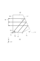
図3(a)〜(d)に、素子100の光104の伝搬方向と直交する面(第2の面)における断面図の一例を示した。結合部材103の反射面107は、第2の面における断面の少なくとも一部は、結晶102側が凹面となる、すなわち、テラヘルツ波の伝搬方向に凸となる曲線を含み、曲線の中心は光104の伝搬方向上に存在している。
FIGS. 3A to 3D show examples of cross-sectional views on a surface (second surface) orthogonal to the propagation direction of the light 104 of the
結合部材103の反射面107は、テラヘルツ波105が反射する反射領域において、光104の伝搬方向と直交する断面における反射面107の長さは、光104の伝搬方向の上流側ほど長くなるように構成されている。換言すると、テラヘルツ波105が反射する反射領域における反射面107の曲率半径は、光104の伝搬方向の下流側ほど小さい。
In the reflection region where the
具体的には、テラヘルツ波105が反射する反射領域において、第1の位置を通り且つ光104の伝搬方向と直交する面における反射面107の曲率半径の方が、第2の位置を通り且つ光104の伝搬方向と直交する面における反射面107の曲率半径より長い。ここで、第2の位置は、第1の位置より光104の伝搬方向の下流側である。よって、光104の伝搬方向の第1の位置を通り且つ光104の伝搬方向と直交する面における反射面107の長さは、第1の位置より光104の伝搬方向の下流側の第2の位置を通り且つ光104の伝搬方向と直交する面における反射面107の長さより長い。
Specifically, in the reflection region where the
換言すると、光104の伝搬方向の下流側で発生したテラヘルツ波を反射する反射領域の光学的なパワーが、光104の伝搬方向の上流側で発生したテラヘルツ波を反射する反射領域の光学的なパワーより大きくなるように、反射面107が構成されている。このような構成にすることで、結晶102から発生したテラヘルツ波105のパワー分布の歪みを低減できる。
In other words, the optical power of the reflection region that reflects the terahertz wave generated downstream in the propagation direction of the light 104 is equal to the optical power of the reflection region that reflects the terahertz wave generated upstream in the propagation direction of the light 104. The reflecting
例えば、図3(a)のように、第2の面における断面が円弧等の曲線を有している構成が挙げられる。この場合、結合部材103に出射するテラヘルツ波105の波面が第1の面301を対称面として円錐状に放射されても、テラヘルツ波105を反射面107における反射によって整形できる。
For example, as shown in FIG. 3A, a configuration in which the cross section of the second surface has a curved line such as an arc is given. In this case, even if the wavefront of the
上述の例に限らず、図3(b)や図3(c)のように、曲線としての円弧の一部が欠けている構成等も適用できる。この場合、発生するテラヘルツ波105のパワーが小さい領域と対応する部分を欠けた構造にすることで、パワーが実質的に大きいテラヘルツ波を整形して取り出すことができる。また、図3(d)に示すような楕円形状を含む構成とすることで、結晶102のz軸方向において収束するビームを形成するなど種々の形態が可能である。
The present invention is not limited to the above example, and a configuration in which a part of an arc as a curve is missing, as shown in FIGS. 3B and 3C, can also be applied. In this case, a terahertz wave having a substantially high power can be shaped and extracted by forming a structure lacking a portion corresponding to a region where the power of the generated
なお、光104の伝搬方向と直交する面における断面図において、反射面107は、第1の面301を対称面として対称であっても良いし、図3(c)のように非対称な部分を有していても良い。
Note that, in the cross-sectional view in the plane orthogonal to the propagation direction of the light 104, the
本実施形態では、反射面107は、光104の伝搬方向を軸とする円錐面の一部を含む形状である。光104の伝搬方向と円錐面の軸とは、テラヘルツ波105の等価波長以下の精度で一致していることが望ましい。これに限らず、任意の直線又は曲線を光104の伝搬方向を軸に回転させてできる曲面の一部を含む形状等の適用できる。
In the present embodiment, the reflecting
反射面107で反射したテラヘルツ波105は、結合部材103の透過面108を透過して外部に出射される。なお、本実施形態ではテラヘルツ波105が透過面108に対して垂直に入射しているが、これに限るものではない。例えば、テラヘルツ波105を透過面108に対してブリュースター角(結合部材103がシリコンの場合には、16.3度)で透過させると、反射によるフレネル損を低減できる。また、結合部材103は反射面107と異なる別の反射面を更に有していても良い。
The
素子100で発生したテラヘルツ波105のパワー分布について説明する。ここでは、比較のため、先行文献2に記載のコリメータを結合部材として用いたテラヘルツ波発生素子1400(以下、「素子1400」と呼ぶ)におけるパワー分布についても述べる。
A power distribution of the
特許文献2を適用した素子1400の構成を、図14に示す。なお、特許文献2は、非線形光学結晶1402(以下、「結晶1402」と呼ぶ)に入射した光1404の第2次高調波を発生させているが、ここでは本実施形態に合わせてテラヘルツ波を発生させる構成に置き換えて考える。第2次高調波とテラヘルツ波とは、非線形結晶中での発生原理こそ異なるものの、チェレンコフ型位相整合により電磁波が導波路から放射される点は同じである。
A structure of an
従来技術を適用した素子1400は、結晶1402を備えた基板1401と、結合部材1403とを有し、結合部材1403は反射面1406を備える。結晶1402と結合部材1403との間には、クラッド層として機能するような部材を配置している。反射面1406は、結晶1402から発生するテラヘルツ波1405を反射する主要な部分の少なくとも一部が円錐面を含み、円錐面の軸は結晶1402を伝搬する光1404の伝搬方向と一致している。
An
チェレンコフ角θcladを50度、テラヘルツ波1405の波長における結合部材1403の屈折率を3.42とすると、特許文献2に記載の式(r=i=j=θclad/2)より、円錐面の半頂角αは25度となる。また、反射面1406に入射するテラヘルツ波1405の入射角iは25度、反射角jは25度となる。
When the Cherenkov angle θ clad is 50 degrees and the refractive index of the
光1404が結晶1402に入射すると、結晶1402から発生したテラヘルツ波1405は、結合部材1403の反射面1406で反射して整形され、結晶1402を伝搬する光1404の伝搬方向と同一の方向に進む。反射面1406で反射したテラヘルツ波1405は、透過面1407を垂直に通過して結合部材1403の外部に放射される。このような構成により、円錐状に放射されたテラヘルツ波1405の波面1408が平面に整形されて外部に放射される。
When the light 1404 enters the
テラヘルツ波のパワー分布について図4を参照して説明する。図4(b)は、2つの素子100、1400それぞれが有する結合部材103、1403から射出したテラヘルツ波の波面106及び1408を、光104、1404の伝搬方向の上流側から見た図である。図4(a)は、図4(b)のA1−A2断面の任意の位置におけるテラヘルツ波のパワー分布図である。素子100で発生したテラヘルツ波105のパワーを丸で示し、素子1400で発生したテラヘルツ波1405のパワーを三角で示す。また、図4(a)の横軸はA1−A2断面における位置を示しており、数値が小さい方がA1側、数値の大きい方がA2側である。
The power distribution of the terahertz wave will be described with reference to FIG. FIG. 4B is a view of the
図4(a)を見ると、素子1400で発生したテラヘルツ波1405のパワー分布は、A1−A2断面のA2側に進むに従ってテラヘルツ波のパワーが著しく低下している。それに対し、本実施形態の素子100で発生したテラヘルツ波105のパワー分布では、どの位置においてもテラヘルツ波のパワーに大きな差はなく、パワー分布の歪みが低減されている。
4A, in the power distribution of the
非線形光学結晶を含む導波路に光を入射させると、導波路上での光のパワーは、導波路の入射端から遠いほど小さくなる。これは、導波路を伝搬するにしたがって光のパルス幅が広くなることが一因である。その他にも、材料分散、導波損失、結晶の不均一性、導波路に入射する際の光の位相特性等の種々の原因によって変わり得ることが分かっている。 When light is incident on a waveguide including a nonlinear optical crystal, the power of the light on the waveguide decreases as the distance from the incident end of the waveguide increases. This is partly because the pulse width of light increases as it propagates through the waveguide. In addition, it has been found that it can vary depending on various causes such as material dispersion, waveguide loss, crystal non-uniformity, and phase characteristics of light when entering the waveguide.
光のパワーの低下に伴い、非線形光学結晶から発生するテラヘルツ波のパワーも光が導波路を伝搬するに従って小さくなる。すなわち、テラヘルツ波のパワーは光の伝搬方向の下流側に進むに従って小さくなり、図5に示したようなパワー分布を示す。 As the power of the light decreases, the power of the terahertz wave generated from the nonlinear optical crystal also decreases as the light propagates through the waveguide. That is, the power of the terahertz wave becomes smaller as it travels downstream in the light propagation direction, and the power distribution as shown in FIG. 5 is shown.
これに対し、反射面107、1406は、どちらも円錐面の一部であるため、テラヘルツ波が反射する位置によって光の伝搬方向と直交する断面における反射面の長さ(以降、単に「反射面の長さ」と呼ぶことがある)が異なることになる。反射面のどの位置に対してもパワーが均一なテラヘルツ波を入射した場合、反射面の長さが長い位置で反射したテラヘルツ波は、拡散されてパワーが小さくなる。それに対し、反射面の長さが短い位置で反射したテラヘルツ波は密度が高く、反射面の長さが長い位置で反射したテラヘルツ波よりパワーが大きくなる。
On the other hand, since the reflecting
先行文献2を適用した素子1400の場合、光1404が結晶1402に入射する入射端側(光の伝搬方向の上流側)で発生したパワーの大きいテラヘルツ波1405ほど、反射面1406の長さが短い部分で反射する。そして、光1404の伝搬方向の下流側で発生したパワーが小さいテラヘルツ波1405ほど、反射面1406の長さが長い部分で反射する。すなわち、パワーの小さいテラヘルツ波1405ほど反射面1406で拡散してパワー密度が低下するため、A1−A2断面におけるパワー分布の歪みが大きくなる。
In the case of the
それに対し、本実施形態の素子100の場合は、パワーの小さいテラヘルツ波105は反射面107の長さが短い部分で反射して、パワーの大きいテラヘルツ波105反射面107の長さが長い部分で反射する構成となっている。すなわち、結晶102を伝搬する光104のパワーの変化がテラヘルツ波105のパワー分布に与える効果と、反射面107の長さがテラヘルツ波105のパワー分布に与える効果と、が逆になっている。その結果、素子100によれば、発生したテラヘルツ波105のパワー分布の歪みを低減できる。
On the other hand, in the case of the
(第2の実施形態)
第2の実施形態のテラヘルツ波発生素子600(以下、「素子600」と呼ぶ)について、図6を参照して説明する。図6は、素子600の構成を説明する図である。第1の実施形態では、結合部材103の反射面107でテラヘルツ波105を全反射させていたが、本実施形態の結合部材601の反射面606は、発生したテラヘルツ波603を一部透過する。
(Second Embodiment)
A terahertz wave generating element 600 (hereinafter referred to as “
素子600は、基板101、結晶(コア層)102を含む導波路201、結合部材601を有する。基板101と導波路201は第1の実施形態と同様の構成で、光602が結晶102を伝搬すると、テラヘルツ波603が発生する。
The
結合部材601は、材料にダイヤモンドを用いる。周波数が1THz付近のテラヘルツ波に対するダイヤモンドの屈折率を2.38とすると、(1)式より、発生したテラヘルツ波605が結合部材603に放射される場合のチェレンコフ角θcladは24度である。
The
反射面606と光の伝搬方向とがなす角の大きさαを(4)式を満たすように設定すると、(5)式より、反射面606に対するテラヘルツ波603の入射角iは12度、反射角jは12度となる。また、反射面606を透過したテラヘルツ波603と反射面606の垂線とがなす角(出射角)kは29度である。
When the angle α between the
ダイヤモンドから空気に出射する際の全反射角は25度であるため、テラヘルツ波603は反射面606で全反射せず、一部が透過する。また、テラヘルツ波603の偏光をz方向の直線偏光としてフレネルの式に従い計算すると、反射面606でのテラヘルツ波603のパワー透過率は79%となる。この透過率は、反射面606を樹脂等でコーティングすることで、任意に調整できる。
Since the total reflection angle at the time of emitting from diamond to the air is 25 degrees, the
光602の伝搬方向の第1の位置を通り且つ光602伝搬方向と直交する断面における反射面606の長さは、第1の位置より光602の伝搬方向の下流側である第2の位置を通り且つ光602の伝搬方向と直交する断面における反射面606の長さより長い。なお、結晶102から発生するテラヘルツ波603が反射する反射領域においてこの条件を満たしていれば良い。すなわち、反射面606は、結晶102から発生するテラヘルツ波603が反射する反射領域における曲率半径が、光602の伝搬方向の下流側ほど小さい。
The length of the reflecting
反射面606で反射した又は反射面606を透過したテラヘルツ波603は、どちらもパワー分布の歪みが低減されて外部に射出される。本実施形態の素子600のように、発生したテラヘルツ波603の一部を透過させるように結合部材を構成することで、整形されて、且つ、パワー分布の歪みが低減されたテラヘルツ波603を2つに分岐して得ることができる。
The terahertz waves 603 reflected by the
また、本実施形態では、光602の伝搬方向と結合部材601の反射面606とがなす角の大きさαは、上述の(4)式を満たすように構成されている。そのため、反射面606で反射したテラヘルツ波603は、波面604が平面となるように整形されて外部に射出される。反射面606を透過したテラヘルツ波603の波面605も平面となるように整形されて外部に射出される。このように、本実施形態によれば、整形され、且つ、パワー分布の歪みを低減したテラヘルツ波を複数取得できる。
In the present embodiment, the angle α formed by the propagation direction of the light 602 and the
反射面606で2つに分岐されたテラヘルツ波603は、それぞれ別々に利用しても良い。また、2つのテラヘルツ波603がそれぞれ結合部材601から射出された後に再び同軸にして、干渉させて検出しても良い。この場合、干渉計は一般に知られている種々の形態が利用可能であり、例えばマイケルソン干渉計などを利用できる。
The terahertz waves 603 branched into two on the
(第3の実施形態)
第3の実施形態について説明する。第1の実施形態では、結晶102から発生したテラヘルツ波105を、結合部材103を介して外部に取り出していた。テラヘルツ波を用いた情報取得装置等におけるテラヘルツ波発生源として用いる場合、取り出したテラヘルツ波を光学系によって試料に導いて測定する。それに対し本実施形態では、素子100の結合部材103の任意の面に試料701を配置して、試料701の測定を行う。その一例として、反射面107に試料701を配置する構成を図7(a)に、透過面108に試料701を配置する構成を図7(b)に示した。
(Third embodiment)
A third embodiment will be described. In the first embodiment, the
本実施形態では、第1の実施形態の素子100と同様の構成のテラヘルツ波発生素子を用いる。すなわち、基板101と結晶102と結合部材103とを有し、結晶102に光104が伝搬するとテラヘルツ波105が発生し、結合部材103に放射される。放射されたテラヘルツ波105は、結合部材103の反射面107で反射される。
In the present embodiment, a terahertz wave generating element having the same configuration as that of the
発生したテラヘルツ波105は、図7(a)に示したように、反射面107に配置された試料701と結合部材103との界面で反射して外部に射出される。また、図7(b)のように、透過面108に試料701を配置して、テラヘルツ波105が反射面107で反射された後、透過面108及び試料701を透過して外部に射出される構成としてもよい。このようにして外部に射出されたテラヘルツ波は105、試料701の光学特性等によって生じる影響を受けており、これを検出して調べることで試料701の情報を取得できる。
As shown in FIG. 7A, the generated
本実施形態によれば、パワー分布の歪みの少ないテラヘルツ波を用いて試料の測定を行うことができる。また、テラヘルツ波を試料に照射するための光学系や空間を外部に設ける必要がなくなり、情報取得装置の小型化に貢献できる。 According to this embodiment, a sample can be measured using a terahertz wave with little distortion in power distribution. In addition, there is no need to provide an external optical system or space for irradiating the sample with terahertz waves, which can contribute to downsizing of the information acquisition apparatus.
(第4の実施形態)
第4の実施形態のテラヘルツ波検出素子800(以下、「素子800」と呼ぶ)について図8を参照して説明する。図8は、素子800の構成を説明する図である。
(Fourth embodiment)
A terahertz wave detection element 800 (hereinafter referred to as “
素子800は、第1の実施形態の素子100と同様の構成である。すなわち、基板101と、結晶(コア層)102と、結合部材103と、を含む。第1〜第3の実施形態がテラヘルツ波発生素子も関するものであったのに対し、本実施形態の素子800は、結合部材103を通って結晶102に到達したテラヘルツ波802を検出する。
The
直線偏光の光801を、その偏光が結晶102のz軸からy軸方向に任意の角度(例えば45度)だけ傾くように、結晶102に入射する。このとき、光801は、結晶102の第1から第3の実施形態で光104を入射した面と対応する面から入射させる。
Linearly
結晶102を伝搬して射出された光801の電界のz軸成分とy軸成分には結晶102の複屈折性によって位相差が生じるため、光801は楕円偏波となる。このような複屈折による位相差は、結晶102として用いる非線形光学結晶の種類、及び、入射偏波方向、導波路201の長さ等によって異なり、構成によっては位相差をゼロにすることもできる。
Since the phase difference occurs between the z-axis component and the y-axis component of the electric field of the light 801 propagating through the
テラヘルツ波802は、波面803が平面となっている状態で結合部材103の透過面108から入射して、反射面107で反射した後、結晶102に集められる。このとき、光801が結晶102を伝搬しているため、テラヘルツ波105の発生とは逆の過程で、結晶102において、テラヘルツ波802と光801との間に相互作用が発生する。
The
なお、光801は、結晶102の素子100で光104を入射した面と対向する面から入射されているため、第1〜第3の実施形態とは光の伝搬方向の上流側と下流側とが逆になる。そのため、本実施形態では、反射面107は、結晶102に入射するテラヘルツ波802の伝搬方向と逆方向に凸である。また、光801の伝搬方向の第1の位置を通り且つ伝搬方向と直交する断面における反射面107の長さは、第1の位置より伝搬方向の上流である第2の位置を通り且つ伝搬方向と直交する断面における反射面107の長さより長いと言える。なお、結晶102に入射するテラヘルツ波802が反射する反射領域において、このような構成となっていれば良い。すなわち、反射面107は、透過面108から入射するテラヘルツ波802が反射する反射領域における曲率半径が、光801の伝搬方向の下流側ほど大きい構成となる。
In addition, since the light 801 is incident from the surface opposite to the surface where the light 104 is incident on the
光801が結晶102を伝搬しているときにテラヘルツ波802が入射すると、テラヘルツ波802の電界によって、結晶102に1次電気光学効果(ポッケルス効果、即ち2次非線形過程の効果の一種)が発生する。そのため、結晶102のz軸の屈折率が変化して、光801の偏波状態が変わる。
When the
その結果、光801のz軸成分は、結晶102の複屈折性によって生じる位相差に加えて、テラヘルツ波802の電界の影響による位相差が生じることになる。それに対して、光801の電界のy軸成分に生じている位相差は、結晶102の複屈折性による位相差のみである。光801のz軸成分に生じる位相差とy軸成分に生じる位相差とが異なるため、結晶102から出射する光801の楕円偏波の楕円率及び主軸の方向等の伝搬状態が変化する。この変化を、外部の偏光素子(不図示)及び光検出器(不図示)等で検出すれば、テラヘルツ波802の電界強度を検出できる。
As a result, the z-axis component of the light 801 has a phase difference due to the influence of the electric field of the
結晶102から出射する光801を検出する方法としては、例えば、ウォラストンプリズムで2つの偏光を分離して、2つの光検出器(不図示)の差動増幅によりS/N比を向上させても良い。なお、差動増幅によるS/N比の向上は必須ではなく、偏光板を利用して1つの光検出器のみでも良い。誘導複屈折の補償のために位相補償板(λ/4板など)を結晶102の出射端と不図示の偏光素子との間に追加してもよい。
As a method for detecting the light 801 emitted from the
本実施形態では、第1〜第3の実施形態で光104を入射した面と対向する面から結晶102に光801を入射しているが、同様の面(端部)から光801を入射してもよい。その場合は、整合する長さが小さくなるため信号強度が小さくなる。
In this embodiment, the light 801 is incident on the
また、本実施形態では、テラヘルツ波802による1次電気光学効果で光801の偏波状態が変化する現象を利用してテラヘルツ波802の影響を調べている。しかし、これに限らず、結晶102を伝搬した光801の位相変化や、結晶102を伝搬した光801の周波数とテラヘルツ波802の周波数との差周波の光信号を検出する、すなわち光のビート信号を検出する方式等も適用できる。
Further, in the present embodiment, the influence of the
テラヘルツ波802の検出感度は、光801の状態とテラヘルツ波802の強度とに依存する。素子800によれば、パワー分布の歪みの少ないテラヘルツ波802が結合部材103に入射しても、テラヘルツ波802が反射面107で反射することによってパワー分布の歪みが大きくなる。そのため、光801がテラヘルツ波802のパワーが大きい部分に到達する位置で検出に適した状態になるように、光801の伝搬状態を調整することで、検出感度を向上できる。
The detection sensitivity of the
本実施形態では、試料を透過又は試料で反射したテラヘルツ波802を、外部から素子800の結合部材103に導き、反射面107を介して結晶102に入射している。しかし、この形態に限らず、図9に示すように素子800の結合部材103の任意の面に試料901を配置する構成にしても良い。図9(a)では、外部から透過面108を透過して結合部材103に入射したテラヘルツ波802は、反射面107に配置された試料901と結合部材103との界面で反射した後、結晶102に入射する。図9(b)では、テラヘルツ波802は外部から試料901及び透過面108を透過して結合部材103に入射した後、反射面107で反射されて結晶102に入射する。
In the present embodiment, a
このような構成にすることで、試料で透過又は反射したテラヘルツ波を検出器に導くための光学系や空間を外部に設ける必要がなくなるため、情報取得装置の小型化に貢献できる。 With such a configuration, it is not necessary to provide an external optical system or space for guiding the terahertz wave transmitted or reflected by the sample to the detector, which can contribute to downsizing of the information acquisition apparatus.
(第5の実施形態)
第5の実施形態について、図10を参照して説明する。図10(a)は、本実施形態におけるテラヘルツ波の発生検出素子1000(以下、「素子1000」と呼ぶ)の構成の一例である。第1から第3の実施形態におけるテラヘルツ波発生素子は、テラヘルツ波を発生させる機能を有し、第4の実施形態の素子800は、別の発生素子で発生したテラヘルツ波を検出する機能を有する。それに対し、本実施形態の素子1000は、1つの素子でテラヘルツ波の発生及び検出を行う。
(Fifth embodiment)
A fifth embodiment will be described with reference to FIG. FIG. 10A shows an example of the configuration of a terahertz wave generation detecting element 1000 (hereinafter referred to as “
素子1000は、基板101と結晶102と結合部材1001とを有する。基板101及び結晶102を含む導波路201は、第1の実施形態と同様の構成である。結合部材1001は、材料及び形状は第1の実施形態の結合部材103と同様だが、結合部材103が反射面107と透過面108とを有するのに対し、結合部材1001は、2つの反射面1005及び1006を有する。
The
素子1000についてより詳細に説明する。発生用の光1002が結晶102を伝搬するとテラヘルツ波1004が発生する。発生したテラヘルツ波1004は、結合部材1001を伝搬して、反射面1006で反射して整形される。その後、テラヘルツ波1004は反射面1005で反射し、反射面1006で再び反射して結晶102に入射する。また、テラヘルツ波1004を検出するための検出用の光1003が、結晶102の光1002が入射した面と対向する面から入射するため、第4の実施形態と同様の手法でテラヘルツ波1004を検出できる。
The
この場合、図10(a)のように、反射面1006に試料1007を配置すれば、試料1007で反射したテラヘルツ波1004を検出して、試料の情報を取得できる。また、図10(b)に示したように、反射面1005に試料1007を配置してもよい。
In this case, as shown in FIG. 10A, if the
本実施形態では、結晶102を含む導波路201を一つ設ける構成としているが、別の導波路を設けて、発生用の光1002を検出用の光1003とをそれぞれ異なる導波路に入射してもよい。また、発生用の光1002と検出用の光1003の光源は、同じであっても良いし異なっていても良い。同じ光源を用いる場合は、結晶102に入射する前にビームスプリッタ等で光を2つに分岐した上で、それぞれを結晶102に入射する。また、テラヘルツ波に変換されずに結晶102から出射した発生用の光1002を、検出用の光1003として用いても良い。
In this embodiment, one
本実施形態の素子1000によれば、発生したテラヘルツ波のパワー分布の歪みを低減して、試料1007の測定を行うことができる。また、検出されるテラヘルツ波1004は、パワー分布に歪みがあるため、結晶102に入射するテラヘルツ波1004のパワーが強い位置で、検出用の光1003が検出に適した状態になるように調整する。このような構成にすれば、検出感度をより向上できる。
According to the
さらに、テラヘルツ波1004をとりまわす光学系を外部に設ける必要がないので、小型の発生検出素子を提供できる。このようなテラヘルツ波の発生検出素子は、内視鏡等の小型プローブ等への適用が期待できる。
Further, since it is not necessary to provide an optical system surrounding the
(第6の実施形態)
第6の実施形態では、第5の実施形態のテラヘルツ波発生検出素子の変形例について、図11を参照して説明する。図11は、本実施形態のテラヘルツ波発生検出素子1100(以下、「素子1100」と呼ぶ)の構成を説明する図である。素子1100は、第1の実施形態の素子100に、わらに三角プリズム1101を有する構成である。
(Sixth embodiment)
In the sixth embodiment, a modification of the terahertz wave generation detection element of the fifth embodiment will be described with reference to FIG. FIG. 11 is a diagram illustrating a configuration of a terahertz wave generation detection element 1100 (hereinafter referred to as “
三角プリズム1101は、結合部材103の透過面108と接して配置されており、三角プリズム1101の全反射面1103に試料1106が配置される。三角プリズム1101は、Siを含むプリズムで、面1104はテラヘルツ波をよく反射する金属等の導電性材料でコーティングされている。
The
三角プリズムの全反射面1103は、テラヘルツ波1102を全反射する面である。ここで、試料1106の屈折率を2と仮定すると、三角プリズム1101から試料1106にテラヘルツ波1102が入射する場合の全反射角は36度である。本実施形態では、試料1106の屈折率が2であると仮定し、全反射面1103に対してテラヘルツ波1102の入射角が45度となるように設定することによって、テラヘルツ波1102が全反射面1103で全反射するように構成する。なお、結合部材103と三角プリズム1101との界面におけるテラヘルツ波1102の反射は、可能な限りゼロに近いことが望ましい。
The
素子1100は、結晶102に発生用の光1107が入射するとテラヘルツ波1102を発生する。発生したテラヘルツ波1102は、反射面107で反射する。その際、テラヘルツ波1102のパワー分布の歪みが低減される。その後、テラヘルツ波1102は、透過面108を透過して三角プリズム1101に入射する。
The
テラヘルツ波1102は、三角プリズム1101を伝搬して全反射面1103と試料1106との界面で全反射した後、面1104で垂直反射して、前述の道筋を逆にたどり結晶102に入射する。このとき、検出用の光1108が結晶102に入射しているため、結晶102から射出した検出用の光1108を分析すれば、第4の実施形態と同様の方法でテラヘルツ波の検出及び試料1106の情報の取得できる。
The
なお、本実施形態では、結合部材103の透過面108と三角プリズム1101とを接して配置しているが、これに限らず、結合部材103と三角プリズム1101とを一体としても良い。また、ここでは三角プリズム1101を用いたが、試料1106が配置されている全反射面1103でテラヘルツ波1102が全反射して、全反射したテラヘルツ波1102が結晶102に入射する構成であれば、プリズムの形状は限定しない。
In the present embodiment, the
本実施形態の素子1100によれば、発生したテラヘルツ波のパワー分布の歪みを低減することができる。また、パワー分布の歪みを低減したテラヘルツ波を用いて試料の測定を行うことができる。
According to the
また、テラヘルツ波をとりまわす光学系を外部に設ける必要がないので、小型の発生検出素子を提供できる。 In addition, since it is not necessary to provide an external optical system for terahertz waves, a small generation detection element can be provided.
(第7の実施形態)
第7の実施形態として、単一周波数のテラヘルツ波の発生について説明する。本実施形態では、第1の実施形態の素子100を用いて、単一周波数のテラヘルツ波を発生する。第1の実施形態では、結晶102に入射する光として超短パルスレーザを用いている。それに対して、本実施形態では、発振周波数の異なる2つの光を結晶102に入射して、単一周波数のテラヘルツ波を発生する。
(Seventh embodiment)
As a seventh embodiment, generation of a single frequency terahertz wave will be described. In the present embodiment, a single-frequency terahertz wave is generated using the
発振周波数の異なる2つの光を出力する光源は、2波長の光を出力するNd:YAGレーザ励起のKTP−OPO(Optical−Parametric−Oscillator)光源や、2台の波長可変レーザダイオード等が挙げられる。2つの光の発振周波数をそれぞれν1、ν2とする。 Examples of the light source that outputs two lights having different oscillation frequencies include an Nd: YAG laser-pumped optical-parametric-oscillator (KTP-OPO) light source that outputs light of two wavelengths, and two wavelength-tunable laser diodes. . The oscillation frequencies of the two lights are ν1 and ν2, respectively.
結晶102に、2つの異なる発振周波数ν1、ν2の光を入射すると、発振周波数ν1と発振周波数ν2との差周波に相当する単一周波数のテラヘルツ波105が発生する。発生した単一周波数のテラヘルツ波105は、上述の各実施形態と同様に、反射面107で反射して、パワー分布の歪みが低減される。
When light having two different oscillation frequencies ν1 and ν2 is incident on the
このような単一周波数のテラヘルツ波の発生方法は、特定の周波数を有するテラヘルツ波で検査やイメージングを行う場合、例えば、医薬品の特定物質の吸収スペクトルに周波数を合わせてその物質の含有量を調べる等の検査に応用できる。 Such a method for generating a single frequency terahertz wave is, for example, when examining or imaging with a terahertz wave having a specific frequency, for example, checking the content of the substance by matching the frequency with the absorption spectrum of a specific substance of a pharmaceutical product It can be applied to such inspections.
本実施形態のような単一周波数のテラヘルツ波を発生する方法は、第1の実施形態に限らず、第2から第6の実施形態に記載したテラヘルツ波発生素子、及び、テラヘルツ波検出素子、発生検出素子にも適用できる。テラヘルツ波検出素子又は発生検出素子の非線形光学結晶に、2つの異なる発振周波数を持つ光を入射させた場合、発振周波数ν1とν2との差周波に相当する単一周波数のテラヘルツ波の検出が可能となる。2つの光の周波数差を変化させれば、所望の周波数のテラヘルツ波の振幅を検出できる。 The method for generating a single-frequency terahertz wave as in this embodiment is not limited to the first embodiment, and the terahertz wave generating element and the terahertz wave detecting element described in the second to sixth embodiments. It can also be applied to a generation detection element. When light having two different oscillation frequencies is incident on the nonlinear optical crystal of the terahertz wave detection element or the generation detection element, it is possible to detect a single frequency terahertz wave corresponding to the difference frequency between the oscillation frequencies ν1 and ν2. It becomes. If the frequency difference between the two lights is changed, the amplitude of the terahertz wave having a desired frequency can be detected.
(第8の実施形態)
本実施形態では、テラヘルツ波を用いた情報取得装置1200(以下、「装置1200」と呼ぶ)について説明する。装置1200はテラヘルツ時間領域分光法(THz−Time−Domain Spectroscopy:THz−TDS)の原理を応用して、テラヘルツ波の時間波形を取得するTHz−TDS装置である。装置1200は、試料1216の情報として、試料1216で反射したテラヘルツ波1230の時間波形を取得する。取得した時間波形を用いれば、試料1216の光学特性及び形状等の情報を取得できる。また、取得した試料1216の情報を基に、画像を形成できる構成としてもよい。
(Eighth embodiment)
In this embodiment, an information acquisition device 1200 (hereinafter referred to as “
図12(a)は、装置1200の構成図である。装置1200は、光源1201、分岐器1202、発生部1204、放物面鏡1205a〜1205d、ビームスプリッタ1206、検出部1207、光学遅延部1209、増幅部1212、変調部1213、信号取得部1214、処理部1215を有する。
FIG. 12A is a configuration diagram of the
光源1201は、光を発生させる光源で、光ファイバを含む。本実施形態では、フェムト秒レーザ(以下、「レーザ光」と呼ぶ)を出力する。
The
光源1201から出力されたレーザ光は、分岐器1202で2つに分岐され、一方はファイバ1203を通って発生部1204に入射し、他方はファイバ1208を通過して検出部1207に到達する。なお、ファイバ1203、1208は、高次ソリトン圧縮を行うための高非線形ファイバや、発生部1204及び検出部1207に至るまでのレーザ光の分散の影響を緩和するためにプリチャープを行う分散ファイバ等を含んでいてもよい。またこれらは偏波保持ファイバであることが望ましい。
Laser light output from the
発生部1204は、テラヘルツ波を発生する部分で、第1の実施形態の素子100を含む。レーザ光が、ファイバ1203を通って発生部1204としての素子100の結晶102に入射することによってテラヘルツ波1230が発生する。発生したテラヘルツ波1230は結合部材103を伝搬して外部に取り出される。
The
レーザ光がファイバ1203から結晶102に入射する際の結合効率を上げるために、ファイバ1203の先端を加工してピッグテール型にする等の方法で、レーザ光の出力が結晶102の開口数(NA)以下になる様に構成すると良い。また、レンズを用いて空間結合しても良い。これらの場合、ファイバ1203及び結晶102の端部に無反射コーティングを施せば、フレネル損失及び不要な干渉ノイズを低減できる。結晶102に対して、ファイバ1203のNA及びモードフィールド径と、結晶102のNA及びモードフィールド径とが近くなる様に設計して直接結合(バットカップリング)により接着しても良い。この場合は、接着剤を適切に選ぶことで反射を低減できる。
In order to increase the coupling efficiency when laser light is incident on the
なお、ファイバ1203や光源1201等に偏波保持でないファイバ部分が含まれる場合、インライン型の偏波コントローラにより発生部1204に入射するレーザ光の偏波を安定化させることが望ましい。
Note that when the
発生部1204からのテラヘルツ波1230は、放物面鏡1205a、1205b、ビームスプリッタ1206、放物面鏡1205cを含む光学系を介して試料1216に照射される。試料1216で反射したテラヘルツ波1230は放物面鏡1205dで集められて検出部1207に入射する。
The terahertz wave 1230 from the
一方、ファイバ1208を通るレーザ光は、光学遅延部1209及びレンズ1210を通過して、試料1216で反射したテラヘルツ波1230とは反対側から検出部1207に入射する。以降、本明細書では、検出部1207に入射するレーザ光をプローブ光と呼ぶ。
On the other hand, laser light passing through the
光学遅延部1209は、検出部1207に入射するテラヘルツ波1230とプローブ光との光路長差を適宜変更して、検出部1207がテラヘルツ波1230を検出するタイミングを調整する部分である。本実施形態では、プローブ光を折り返す折り返し光学系と折り返し光学系を動かす可動部とを用いて、プローブ光が検出部1207に入射するまでの光路長を変更する。
The
光学遅延部1209は、上述の構成に限らず、可動部に回転する系等を適用しても良い。また、プローブ光の伝搬経路中の屈折率等を調整して光路長を変化させる方法等も適用できる。上述の方法を用いてプローブ光ではなく、光源1201から発生部1204に入射するまでのレーザ光の光路長を変更しても良い。
The
検出部1207は、テラヘルツ波1230を検出する部分で、低温成長させたGaAsにダイポールアンテナを形成した光伝導素子を用いる。光源1201から出力されるレーザ光の波長が1.55μmであれば、不図示のSHG結晶(Second Harmonic Generation結晶)をプローブ光の伝搬経路に配置しても良い。SHG結晶を用いて2倍波を生成すれば、GaAsを励起するのに適したプローブ光を得ることができ、精度の良い検出が可能となる。
The
SHG結晶としては、レーザ光のパルス形状を維持するために、0.1mm程度の厚さのPPLN結晶(周期的極性反転リチウムナイオベイト)を用いることが望ましい。なお、本実施形態のようにパルス幅が十分に小さい場合には基本波をそのままプローブ光として利用できる。 As the SHG crystal, it is desirable to use a PPLN crystal (periodic polarity inversion lithium niobate) having a thickness of about 0.1 mm in order to maintain the pulse shape of the laser beam. If the pulse width is sufficiently small as in this embodiment, the fundamental wave can be used as it is as the probe light.
検出部1207で検出された信号は位相敏感検波されて、その出力信号が増幅部1212で増幅されて信号取得部1214に送られる。オプティカルチョッパー1211は位相敏感検波を行うためにプローブ光を変調する部分で、変調部1213によって制御されている。
The signal detected by the
信号取得部1214は、検出部1207からの出力信号を取得する部分である。処理部1215は、信号取得部1214が取得した出力信号を基に時間波形を取得して、その時間波形を調べることで、試料1216の情報を取得する。取得した試料1216の情報に基づいて試料1216の内部構造の画像を取得することもできる。
The
試料1216の内部構造のイメージングについては、試料1216の内部に屈折率が異なる部分(界面)があれば、界面の深さに応じて、時間波形上の異なる位置の各界面で反射したテラヘルツ波の時間波形が現れる。そのため、試料1216を1次元でスキャンすれば断層画像が取得でき、2次元でスキャンすれば3次元画像を取得できる。
As for imaging of the internal structure of the
なお、本実施形態では、放物面鏡1205cで集光されて試料1216に照射されるテラヘルツ波1230と試料1216からの反射波とテラヘルツ波とが同軸である。そのため、2つのテラヘルツ波1230をビームスプリッタ1206で分岐するため、テラヘルツ波1230のパワーが減少する。よって、図12(b)のように、新たに放物面鏡1205eを1つ又は複数設けて非同軸の構成にしても良い。この場合、試料1216に照射されるテラヘルツ波1230の入射角が90度でなくなるが、検出されるテラヘルツ波の出力を大きくできる。
In the present embodiment, the terahertz wave 1230 collected by the
本実施形態では、発生部1204として第1の実施形態の素子100を用いているが、第1〜第3の実施形態に記載のテラヘルツ波発生素子等を用いても良い。第3の実施形態の素子を用いる場合は、発生部1204からのテラヘルツ波1230を試料1216に導くための光学系は設けなくて良い。
In the present embodiment, the
また、本実施形態では、検出部1207に光伝導素子を用いているが、これを第4又は第5の実施形態に記載のテラヘルツ波検出素子又はその他のテラヘルツ波検出素子に置き換えることも可能である。検出部1207として第4、第5の実施形態のテラヘルツ波検出素子を用いる場合、発生部1204の構成は限定されず、前述の実施形態に記載のテラヘルツ波発生素子を用いても良いし、光伝導素子等の公知のテラヘルツ波発生素子を用いても良い。第5の実施形態の素子1000を用いる場合は、試料1216で反射したテラヘルツ波1230を検出部1207に導くための光学系は設けなくて良い。
In this embodiment, a photoconductive element is used for the
また、発生部1204及び検出部1207を、第5及び第6の実施形態のような発生検出素子で置き換えることで、1つの発生検出部としても良い。この場合、発生部1204からのテラヘルツ波1230を試料1216に導くための光学系、及び、試料1216からのテラヘルツ波1230を検出部1207に導くための光学系を設けなくて良い。また、装置1200は、試料1216で反射したテラヘルツ波1230を検出する構成としているが、試料1216を透過したテラヘルツ波1230を検出する構成でもよい。
Further, the
第1から第7の実施形態に記載のテラヘルツ波発生素子、テラヘルツ波検出素子、テラヘルツ波発生検出素子は、本実施形態のTHz−TDS装置に限らず、他の情報取得装置にも用いることができる。 The terahertz wave generation element, the terahertz wave detection element, and the terahertz wave generation detection element described in the first to seventh embodiments are not limited to the THz-TDS apparatus according to the present embodiment, and may be used for other information acquisition apparatuses. it can.
以上、本実施形態の装置1200によれば、発生部1204として素子100を用いることで、パワー分布の歪みが低減されたテラヘルツ波を用いて試料1216の測定を行うことができる。そのため、分解能の高い測定が可能となる。また、パワー分布の歪みが低減されているため、試料1216に照射されるテラヘルツ波のパワーが大きくなるため、S/N比の向上が期待できる。さらに、本実施形態では、ファイバを用いて光学系を構成しているので、装置1200の小型化が期待できる。
As described above, according to the
(実施例1)
第1の実施形態の素子100の構成をより具体的に説明する。導波路201の長さは10mmである。導波路201に含まれるコア層102は、幅5μm、厚さ3.8μmのMgOドープLN結晶層で形成されている。コア層102の上部には、幅5μm、厚さ2μmの上部クラッド層202が形成されている。上部クラッド層202は、コア層102と結合部材103とを接着するための光学接着剤である。
Example 1
The configuration of the
上部クラッド層202の厚さは、発生するテラヘルツ波105の波長から決定する。テラヘルツ波105の最大周波数が7THzであった場合、テラヘルツ波105の自由空間における波長は約43μmである。前述のように、上部クラッド層202の厚みは、λeq/10以下であることが望ましい。緩衝層の屈折率が1.5である場合、λeq/10=2.85となるため、この厚さ以下になるように上部クラッド層202の厚さを2μmにした。
The thickness of the
結合部材103には、高抵抗Siを用いた。結合部材103の反射面107は、円錐面の一部を切り取ったような形状をしており、円錐面の軸109と光104の伝搬方向とが一致するように構成されている。このとき、光104の伝搬方向を含む面において、光104の伝搬方向と反射面107とがなす角αは65度である。結合部材103の大きさは、導波路201の入射端から円錐面の頂点110までの距離を約18mmとした。
High resistance Si was used for the
本実施例におけるチェレンコフ角θcladは50度である。また、テラヘルツ波105が反射面107に入射する場合に、テラヘルツ波105と反射面107の垂線とがなす角(入射角)iと反射面107で反射したテラヘルツ波105と反射面107の垂線とがなす角(反射角)jは、ともに25度である。
In this embodiment, the Cerenkov angle θ clad is 50 degrees. In addition, when the
結晶102に入射する光104は、ピーク波長1.6μm、パルス幅20fs、平均パワー60mWで、ビーム径(最大強度に対して1/e2以上の強度部分の径)を6μmとした超短パルスレーザである。光104が、結晶102の端面から入射して結晶102をシングルモードで伝搬すると、テラヘルツ波105が発生して、チェレンコフ放射によって円錐状に放射される。
The light 104 incident on the
放射されたテラヘルツ波105は結合部材103に伝搬して、反射面107で反射される。結合部材103を形成する高抵抗Siと空気との界面における全反射角は約17度なので、テラヘルツ波105は反射面107で全反射される。反射面107で反射されたテラヘルツ波105は、透過面108を通過して結合部材103の外部の空間へ放射される。
The radiated
本実施例の素子100によれば、テラヘルツ波の波面をほぼ平面に整形しつつ、パワー分布の歪みの小さいテラヘルツ波を得ることができる。
According to the
以上、本発明の好ましい実施形態について説明したが、本発明はこれらの実施形態に限定されず、その要旨の範囲内で種々の変形及び変更が可能である。 As mentioned above, although preferable embodiment of this invention was described, this invention is not limited to these embodiment, A various deformation | transformation and change are possible within the range of the summary.
例えば、上述の実施形態及び実施例では、非線形光学結晶102の幅が小さく、幅を持たない点光源とみなせる場合について説明した。しかし、これに限らず、非線形光学結晶102が実質的に幅を持つ場合でも本発明を適用できる。
For example, in the above-described embodiments and examples, the case where the nonlinear
この場合、光の伝搬方向と直交する面におけるテラヘルツ波105の波面に応じて、光の伝搬方向と直交する断面における結合部材103の反射面107の形状を変更すると良い。一例として、図3(d)に示すような楕円形状に近い形態が考えられる。このような形状にすることで、反射面107で反射したテラヘルツ波のパワー分布の歪みを低減して、波面を平行に近づけることができる。
In this case, the shape of the
また、上述の実施形態及び実施例では、光の伝搬方向を含む面において反射面が直線である場合を挙げたが、直線でなく曲線である構成としても良い。この時、反射面と光の伝搬方向とがなす角の大きさαは、反射面を構成する曲線の接線と光の伝搬方向とがなす角の大きさとする。 In the above-described embodiments and examples, the case where the reflecting surface is a straight line in the plane including the light propagation direction has been described, but a configuration in which the reflecting surface is not a straight line but a curve may be employed. At this time, the angle α formed by the reflecting surface and the light propagation direction is the angle formed by the tangent of the curve forming the reflecting surface and the light propagation direction.
また、上述の実施形態及び実施例では、非線形光学結晶としてLNを用いているが、これに限らずその他の非線形光学結晶を用いることもできる。LNは、テラヘルツ波に対する屈折率とレーザ光に対する屈折率との差が十分に大きいため、ノンコリニアで発生するテラヘルツ波を取り出すことが可能である。 In the above-described embodiments and examples, LN is used as the nonlinear optical crystal. However, the present invention is not limited to this, and other nonlinear optical crystals can also be used. Since LN has a sufficiently large difference between the refractive index for the terahertz wave and the refractive index for the laser beam, it is possible to extract the terahertz wave generated in a non-collinear manner.
しかし、使用する非線形光学結晶によっては該屈折率差が小さく、発生したテラヘルツ波を容易に取り出せないことがある。その場合、非線形光学結晶102と結合部材103とが近接するように導波路201を設けて、結合部材103の材料に非線形光学結晶よりも屈折率が大きいものを用いれば良い。このような構成にすることで、発生した電磁波がチェレンコフ放射するための条件(VTHz<Vg)を満たし、テラヘルツ波を外部に取り出すことができる。
However, depending on the nonlinear optical crystal used, the refractive index difference is small, and the generated terahertz wave may not be easily extracted. In that case, a
テラヘルツ波発生素子については、テラヘルツ波の出力を大きくするために、導波路201の長さ(x方向の長さ)を長くしても良い。この場合、発生するテラヘルツ波をより多く利用できるように、結合部材103の大きさも導波路201の長さに合わせて変更すると良い。
For the terahertz wave generating element, the length of the waveguide 201 (the length in the x direction) may be increased in order to increase the output of the terahertz wave. In this case, the size of the
また、基板101についても上述の実施形態に限らず、種々の変更が可能である。例えば、基板101の大きさは、導波路201を保持できる範囲で小さくできる。また、基板101の裏面、すなわち、導波路201が形成されている面と対向する面の構成を変更できる。具体的には、基板101の裏面で反射する光が迷光となるのを防ぐために斜めにカットしたり、基板101の裏面にもテラヘルツ波が放射される構成の場合は、プリズムやレンズを配置したりしても良い。材料も、Siや樹脂など種々の物質を使用できる。また、基板101を設けない構成とすることも可能である。
Further, the
102 非線形光学結晶
103 結合部材
107 反射面
102 Nonlinear
Claims (18)
前記非線形光学結晶から発生するテラヘルツ波が伝搬する結合部材と、を有し、
前記結合部材は、前記非線形光学結晶から発生するテラヘルツ波の少なくとも一部を反射する反射面と、前記反射面で反射したテラヘルツ波を透過する透過面と、を有し、
前記反射面は、前記非線形光学結晶から発生するテラヘルツ波の伝搬方向に凸であり、前記光の波長における前記非線形光学結晶の群屈折率をng、前記非線形光学結晶から発生するテラヘルツ波の波長における前記結合部材の屈折率をnTHzとすると、前記光の伝搬方向を含む面において、前記反射面と前記光の伝搬方向とがなす前記結合部材側の角の大きさは、90度−cos−1(ng/nTHz)より大きく且つ90度より小さく、前記非線形光学結晶から発生するテラヘルツ波が反射する反射領域における前記反射面の曲率半径は、前記光の伝搬方向の下流側ほど小さい
ことを特徴とするテラヘルツ波発生素子。A nonlinear optical crystal that generates terahertz waves by the propagation of light; and
And a coupling member for propagating terahertz waves generated from the nonlinear optical crystal,
The coupling member has a reflection surface that reflects at least a part of the terahertz wave generated from the nonlinear optical crystal, and a transmission surface that transmits the terahertz wave reflected by the reflection surface,
The reflection surface is convex in the propagation direction of the terahertz wave generated from the nonlinear optical crystal, the group refractive index of the nonlinear optical crystal at the wavelength of the light is ng, and the wavelength of the terahertz wave generated from the nonlinear optical crystal is Assuming that the refractive index of the coupling member is n THz, the angle on the coupling member side formed by the reflection surface and the light propagation direction on the plane including the light propagation direction is 90 degrees −cos −1. It is larger than (ng / nTHHz) and smaller than 90 degrees, and the radius of curvature of the reflecting surface in the reflection region where the terahertz wave generated from the nonlinear optical crystal is reflected is smaller toward the downstream side in the light propagation direction. Terahertz wave generator.
ことを特徴とする請求項1に記載のテラヘルツ波発生素子。When the refractive index of the substance outside the coupling member at the wavelength of the terahertz wave generated from the nonlinear optical crystal is represented by ne, the size of the angle is sin −1 (ne / n THz) +90 degrees−cos −1 (ng The terahertz wave generating element according to claim 1, wherein the terahertz wave generating element is equal to or higher than / n THz.
ことを特徴とする請求項1または2に記載のテラヘルツ波発生素子。 The terahertz wave generated from the nonlinear optical crystal, the terahertz wave generating device according to claim 1 or 2, characterized in that the total reflection at the reflecting surface.
ことを特徴とする請求項1乃至3のいずれか一項に記載のテラヘルツ波発生素子。 The reflective surface, the terahertz wave generating device according to any one of claims 1 to 3, characterized in that it comprises a portion of the curved surface can be a line or curve by rotating the propagation direction of the light axis.
ことを特徴とする請求項1乃至4のいずれか一項に記載のテラヘルツ波発生素子。 The reflective surface, the terahertz wave generating device according to any one of claims 1 to 4, characterized in that it comprises a portion of a conical surface that the propagation direction of the light and the axis.
ことを特徴とする請求項1乃至5のいずれか一項に記載のテラヘルツ波発生素子。 The reflective surface, according to any one of claims 1 to 5 wherein the coupling member at least a portion of the cross section of the plane orthogonal to the propagation direction of the light is equal to or is a part of a circle or ellipse Terahertz wave generator.
ことを特徴とする請求項1乃至6のいずれか一項に記載のテラヘルツ波発生素子。 Plane including the propagation direction of the light, the terahertz wave generating device according to any one of claims 1 to 6, characterized in that is perpendicular to the surface of the nonlinear optical crystal.
前記導波路は、前記非線形光学結晶と、前記非線形光学結晶と前記結合部材との間に設けられ且つ前記光の波長における前記非線形光学結晶の屈折率より低い屈折率を有するクラッド層と、を有する
ことを特徴とする請求項1乃至7のいずれか一項に記載のテラヘルツ波発生素子。 Having a waveguide,
The waveguide includes the nonlinear optical crystal, and a clad layer provided between the nonlinear optical crystal and the coupling member and having a refractive index lower than that of the nonlinear optical crystal at the wavelength of the light. a terahertz wave generating device according to any one of claims 1 to 7, characterized in that.
ことを特徴とする請求項1乃至8のいずれか一項に記載のテラヘルツ波発生素子。 The width of the nonlinear optical crystal in a direction orthogonal to the light propagation direction and not orthogonal to the principal surface of the nonlinear optical crystal is the wavelength of the terahertz wave generated from the nonlinear optical crystal. The terahertz wave generating element according to any one of claims 1 to 8 , wherein the terahertz wave generating element is smaller.
ことを特徴とする請求項1乃至9のいずれか一項に記載のテラヘルツ波発生素子。 The nonlinear optical crystal is configured to change the propagation state of light different from the light when the terahertz wave generated from the nonlinear optical crystal is incident again. The terahertz wave generating element according to any one of claims 1 to 9 , wherein a terahertz wave generated from the nonlinear optical crystal is detected.
前記結合部材は、テラヘルツ波を透過する透過面と、前記透過面を透過したテラヘルツ波の少なくとも一部を反射する反射面と、を有し、
前記反射面は、前記非線形光学結晶に入射するテラヘルツ波の伝搬方向と逆方向に凸であり、
前記光の波長における前記非線形光学結晶の群屈折率をng、前記非線形光学結晶から発生するテラヘルツ波の波長における前記結合部材の屈折率をnTHzとすると、前記光の伝搬方向を含む面において、前記反射面と前記光の伝搬方向とがなす前記結合部材側の角の大きさは、90度−cos−1(ng/nTHz)より大きく且つ90度より小さく、
前記非線形光学結晶から発生するテラヘルツ波が反射する反射領域における前記反射面の曲率半径は、前記光の伝搬方向の下流側ほど大きい
ことを特徴とするテラヘルツ波検出素子。A non-linear optical crystal whose propagation state of light changes when a terahertz wave is incident, and a coupling member that guides the terahertz wave to the non-linear optical crystal,
The coupling member has a transmission surface that transmits the terahertz wave, and a reflection surface that reflects at least a portion of the terahertz wave that has transmitted the transmission surface,
The reflecting surface is convex in the direction opposite to the propagation direction of the terahertz wave incident on the nonlinear optical crystal,
When the group refractive index of the nonlinear optical crystal at the wavelength of the light is ng and the refractive index of the coupling member at the wavelength of the terahertz wave generated from the nonlinear optical crystal is n THz, the plane including the light propagation direction is The size of the angle on the coupling member side formed by the reflection surface and the light propagation direction is greater than 90 degrees −cos −1 (ng / n THz) and smaller than 90 degrees.
A terahertz wave detecting element, wherein a radius of curvature of the reflecting surface in a reflection region where a terahertz wave generated from the nonlinear optical crystal is reflected is larger toward a downstream side in the light propagation direction.
テラヘルツ波を発生する発生部と、
前記試料を透過した又は前記試料で反射したテラヘルツ波を検出する検出部と、を有し、
前記発生部は、請求項1乃至10のいずれか一項に記載のテラヘルツ波発生素子を含むことを特徴とする情報取得装置。 An information acquisition apparatus for acquiring information on a sample by irradiating the sample with terahertz waves,
A generator that generates terahertz waves;
Detecting a terahertz wave transmitted through the sample or reflected by the sample,
The information generation apparatus, wherein the generation unit includes the terahertz wave generation element according to any one of claims 1 to 10 .
ことを特徴とする請求項12に記載の情報取得装置。 The information acquisition apparatus according to claim 12 , wherein the generation unit and the detection unit are integrally configured, and the terahertz wave generation element functions as the generation unit and the detection unit.
テラヘルツ波を発生する発生部と、
前記試料からのテラヘルツ波を検出する検出部と、を有し、
前記検出部は、請求項11に記載のテラヘルツ波検出素子を含む
ことを特徴とする情報取得装置。 An information acquisition apparatus for acquiring information on a sample by irradiating the sample with terahertz waves,
A generator that generates terahertz waves;
A detection unit for detecting terahertz waves from the sample,
The information acquisition device, wherein the detection unit includes the terahertz wave detection element according to claim 11 .
前記結晶中を光が伝搬することによって発生するテラヘルツ波が、伝搬する結合部材と、を有し、A terahertz wave generated by light propagating through the crystal, and a coupling member that propagates,
前記結合部材は、前記テラヘルツ波の少なくとも一部を反射する反射面と、前記反射面で反射した前記テラヘルツ波を透過させる透過面と、を有し、The coupling member has a reflection surface that reflects at least a part of the terahertz wave, and a transmission surface that transmits the terahertz wave reflected by the reflection surface,
前記反射面は、前記光の伝搬方向の下流側に頂点を有する円錐面の一部を含むことを特徴とするテラヘルツ波発生素子。The terahertz wave generating element, wherein the reflecting surface includes a part of a conical surface having a vertex on the downstream side in the light propagation direction.
Priority Applications (4)
| Application Number | Priority Date | Filing Date | Title |
|---|---|---|---|
| JP2014182737A JP6456078B2 (en) | 2013-10-09 | 2014-09-08 | Terahertz wave generating element and terahertz wave detecting element |
| US15/027,361 US10180619B2 (en) | 2013-10-09 | 2014-09-24 | Terahertz wave generating element and terahertz wave detecting element |
| PCT/JP2014/076232 WO2015053138A1 (en) | 2013-10-09 | 2014-09-24 | Terahertz wave generating element and terahertz wave detecting element |
| CN201480055758.3A CN105637411A (en) | 2013-10-09 | 2014-09-24 | Terahertz wave generating element and terahertz wave detecting element |
Applications Claiming Priority (3)
| Application Number | Priority Date | Filing Date | Title |
|---|---|---|---|
| JP2013212295 | 2013-10-09 | ||
| JP2013212295 | 2013-10-09 | ||
| JP2014182737A JP6456078B2 (en) | 2013-10-09 | 2014-09-08 | Terahertz wave generating element and terahertz wave detecting element |
Publications (3)
| Publication Number | Publication Date |
|---|---|
| JP2015096941A JP2015096941A (en) | 2015-05-21 |
| JP2015096941A5 JP2015096941A5 (en) | 2017-10-12 |
| JP6456078B2 true JP6456078B2 (en) | 2019-01-23 |
Family
ID=51844809
Family Applications (1)
| Application Number | Title | Priority Date | Filing Date |
|---|---|---|---|
| JP2014182737A Active JP6456078B2 (en) | 2013-10-09 | 2014-09-08 | Terahertz wave generating element and terahertz wave detecting element |
Country Status (4)
| Country | Link |
|---|---|
| US (1) | US10180619B2 (en) |
| JP (1) | JP6456078B2 (en) |
| CN (1) | CN105637411A (en) |
| WO (1) | WO2015053138A1 (en) |
Families Citing this family (11)
| Publication number | Priority date | Publication date | Assignee | Title |
|---|---|---|---|---|
| WO2016022757A1 (en) * | 2014-08-06 | 2016-02-11 | University Of Massachusetts | Single channel terahertz endoscopy |
| CN106052873B (en) * | 2016-05-27 | 2018-04-20 | 北京环境特性研究所 | THz wave coherence detector and terahertz polarization detection method based on gas |
| CN107063476B (en) * | 2017-05-27 | 2019-05-17 | 中国电子科技集团公司第四十一研究所 | A kind of device and method measuring Terahertz wavelength |
| JP7014623B2 (en) * | 2018-01-29 | 2022-02-01 | 浜松ホトニクス株式会社 | Terahertz wave spectroscopic measuring device |
| CN109244800B (en) * | 2018-10-11 | 2021-02-26 | 华北水利水电大学 | Quasi-phase matching terahertz wave parametric oscillator |
| CN109167236B (en) * | 2018-10-11 | 2020-12-01 | 华北水利水电大学 | Three-dimensional terahertz wave parametric oscillator |
| CN109193315B (en) * | 2018-10-11 | 2021-03-30 | 华北水利水电大学 | Double-frequency terahertz wave parametric oscillator |
| CN109301681B (en) * | 2018-10-11 | 2021-01-29 | 华北水利水电大学 | High-efficiency terahertz wave parametric oscillator |
| CN109119871B (en) * | 2018-10-11 | 2020-12-01 | 华北水利水电大学 | Annular cavity terahertz wave parametric oscillator |
| CN110783801B (en) * | 2019-10-31 | 2021-07-27 | 郑州轻工业学院 | THz wave parameter source for multi-wavelength pulse delay output |
| CN115390336B (en) * | 2022-09-14 | 2024-05-24 | 中国电子科技集团公司第四十一研究所 | Optical difference frequency terahertz wave generation device and method based on lithium niobate crystal |
Family Cites Families (13)
| Publication number | Priority date | Publication date | Assignee | Title |
|---|---|---|---|---|
| JP2738713B2 (en) | 1988-09-19 | 1998-04-08 | 株式会社日立製作所 | Second harmonic generator |
| GB0119564D0 (en) * | 2001-08-10 | 2001-10-03 | Univ Cambridge Tech | Radiation device |
| JP4749156B2 (en) * | 2004-01-29 | 2011-08-17 | 潤一 西澤 | Electromagnetic wave generator |
| DE102007025891A1 (en) * | 2007-06-01 | 2008-12-11 | Johann Wolfgang Goethe-Universität Frankfurt am Main | Apparatus and method for generating and detecting coherent electromagnetic radiation in the THz frequency range |
| JP5354582B2 (en) | 2009-03-04 | 2013-11-27 | 国立大学法人名古屋大学 | Terahertz wave generator |
| KR101076396B1 (en) * | 2009-08-06 | 2011-10-25 | 한국과학기술연구원 | Simultaneous generation devices of Terahertz wave and Supercontinuum, Method there of and Spectroscopy method using the same |
| JP5967867B2 (en) * | 2010-06-03 | 2016-08-10 | キヤノン株式会社 | Terahertz wave generating element, terahertz wave detecting element, and terahertz time domain spectroscopic device |
| JP5885414B2 (en) * | 2010-08-05 | 2016-03-15 | キヤノン株式会社 | Optical frequency conversion element |
| JP2012053450A (en) * | 2010-08-05 | 2012-03-15 | Canon Inc | Terahertz wave generating element, terahertz wave detecting element, terahertz wave generator, terahertz wave detector, terahertz wave measuring instrument, and terahertz wave tomographic imaging apparatus |
| JP6075822B2 (en) * | 2012-03-13 | 2017-02-08 | キヤノン株式会社 | Sensor device |
| JP5973774B2 (en) * | 2012-04-27 | 2016-08-23 | 株式会社アドバンテスト | Electromagnetic radiation device |
| JP2015038599A (en) * | 2013-07-18 | 2015-02-26 | キヤノン株式会社 | Terahertz wave generating device and information acquisition device |
| JP2017138461A (en) * | 2016-02-03 | 2017-08-10 | 澁谷工業株式会社 | Terahertz light generator |
-
2014
- 2014-09-08 JP JP2014182737A patent/JP6456078B2/en active Active
- 2014-09-24 WO PCT/JP2014/076232 patent/WO2015053138A1/en active Application Filing
- 2014-09-24 US US15/027,361 patent/US10180619B2/en active Active
- 2014-09-24 CN CN201480055758.3A patent/CN105637411A/en not_active Withdrawn
Also Published As
| Publication number | Publication date |
|---|---|
| US10180619B2 (en) | 2019-01-15 |
| WO2015053138A9 (en) | 2015-05-14 |
| WO2015053138A4 (en) | 2015-06-11 |
| WO2015053138A1 (en) | 2015-04-16 |
| US20160246158A1 (en) | 2016-08-25 |
| CN105637411A (en) | 2016-06-01 |
| JP2015096941A (en) | 2015-05-21 |
Similar Documents
| Publication | Publication Date | Title |
|---|---|---|
| JP6456078B2 (en) | Terahertz wave generating element and terahertz wave detecting element | |
| US10331010B2 (en) | Terahertz-wave generating element terahertz-wave detecting element and terahertz time-domain spectroscopy device | |
| JP5943594B2 (en) | Terahertz wave element, terahertz wave detection device, terahertz time domain spectroscopy system, and tomography device | |
| US9304373B2 (en) | Terahertz wave generation element, terahertz wave detection element, and terahertz time domain spectroscope device | |
| JP5885414B2 (en) | Optical frequency conversion element | |
| US20150136987A1 (en) | Terahertz wave generator, terahertz wave detector, and terahertz time domain spectroscopy device | |
| US8759779B2 (en) | Terahertz wave generation element, terahertz wave detection element, and terahertz time domain spectral device | |
| JP2012053450A (en) | Terahertz wave generating element, terahertz wave detecting element, terahertz wave generator, terahertz wave detector, terahertz wave measuring instrument, and terahertz wave tomographic imaging apparatus | |
| US9244331B2 (en) | Electromagnetic wave generating device, electromagnetic wave detecting device, and time-domain spectroscopy apparatus | |
| JP6328202B2 (en) | Terahertz wave generating element and terahertz time domain spectrometer | |
| US20160274306A1 (en) | Optical transmission apparatus and transmission method therefor |
Legal Events
| Date | Code | Title | Description |
|---|---|---|---|
| A521 | Written amendment |
Free format text: JAPANESE INTERMEDIATE CODE: A523 Effective date: 20170904 |
|
| A621 | Written request for application examination |
Free format text: JAPANESE INTERMEDIATE CODE: A621 Effective date: 20170904 |
|
| A131 | Notification of reasons for refusal |
Free format text: JAPANESE INTERMEDIATE CODE: A131 Effective date: 20180807 |
|
| A521 | Written amendment |
Free format text: JAPANESE INTERMEDIATE CODE: A523 Effective date: 20181003 |
|
| TRDD | Decision of grant or rejection written | ||
| A01 | Written decision to grant a patent or to grant a registration (utility model) |
Free format text: JAPANESE INTERMEDIATE CODE: A01 Effective date: 20181120 |
|
| A61 | First payment of annual fees (during grant procedure) |
Free format text: JAPANESE INTERMEDIATE CODE: A61 Effective date: 20181218 |
|
| R151 | Written notification of patent or utility model registration |
Ref document number: 6456078 Country of ref document: JP Free format text: JAPANESE INTERMEDIATE CODE: R151 |