JP6456013B2 - Apparatus, method, and program for performing dither processing - Google Patents
Apparatus, method, and program for performing dither processing Download PDFInfo
- Publication number
- JP6456013B2 JP6456013B2 JP2013080804A JP2013080804A JP6456013B2 JP 6456013 B2 JP6456013 B2 JP 6456013B2 JP 2013080804 A JP2013080804 A JP 2013080804A JP 2013080804 A JP2013080804 A JP 2013080804A JP 6456013 B2 JP6456013 B2 JP 6456013B2
- Authority
- JP
- Japan
- Prior art keywords
- dither matrix
- image data
- scanning direction
- light emitting
- threshold
- Prior art date
- Legal status (The legal status is an assumption and is not a legal conclusion. Google has not performed a legal analysis and makes no representation as to the accuracy of the status listed.)
- Active
Links
Images


Classifications
-
- H—ELECTRICITY
- H04—ELECTRIC COMMUNICATION TECHNIQUE
- H04N—PICTORIAL COMMUNICATION, e.g. TELEVISION
- H04N1/00—Scanning, transmission or reproduction of documents or the like, e.g. facsimile transmission; Details thereof
- H04N1/40—Picture signal circuits
- H04N1/405—Halftoning, i.e. converting the picture signal of a continuous-tone original into a corresponding signal showing only two levels
Description
ディザ処理に関する。 It relates to dither processing.
電子写真方式のプリンタにおいては、LEDや有機ELを用いた露光ヘッドを用いて、感光体ドラムを露光し、潜像形成を行う方式が一般的に知られている。前記露光ヘッドは、感光体ドラムの長手方向に配列した発光素子群と、前記発光素子群の光を感光体ドラム上に結像するロッドレンズアレイで構成される。ここで、発光素子群の長さは感光体ドラム上における画像領域幅に応じて長さが決まり、プリンタの解像度に応じて素子間隔が決まる。画像領域幅としてA3サイズに対応した感光ドラムの長さはおよそ310mm程度であり、1200dpiの解像度の場合、発光素子約15,000個(310×1200÷25.4)で構成される。また、この場合の発光素子の間隔、すなわち画素の間隔は21.2μm(小数点2桁以降は省略)となる。 In an electrophotographic printer, a method is generally known in which an exposure head using an LED or an organic EL is used to expose a photosensitive drum to form a latent image. The exposure head includes a light emitting element group arranged in the longitudinal direction of the photosensitive drum, and a rod lens array that images light from the light emitting element group on the photosensitive drum. Here, the length of the light emitting element group is determined according to the width of the image area on the photosensitive drum, and the element interval is determined according to the resolution of the printer. The length of the photosensitive drum corresponding to the A3 size as the image area width is about 310 mm, and in the case of a resolution of 1200 dpi, it is composed of about 15,000 light emitting elements (310 × 1200 ÷ 25.4). In this case, the interval between the light emitting elements, that is, the interval between the pixels is 21.2 μm (2 digits after the decimal point are omitted).
このような露光ヘッドを用いたプリンタでは、レーザービームをポリゴンモータで偏光走査するレーザ走査方式のプリンタと比較して、使用する部品数が少ないため、装置の小型化、低コスト化が容易である。しかし、LEDや有機EL等の発光素子は、経時的に光量が低下するという光量劣化特性を持ち、特に有機ELは劣化速度が速い。発光素子毎の使用頻度が異なる場合、素子劣化の進行が素子毎にばらつくため、光量ばらつきが発生する。その結果、画像にスジ等の画像不良が発生するという問題が発生していた。 In a printer using such an exposure head, the number of parts used is small compared to a laser scanning printer that performs polarization scanning of a laser beam with a polygon motor, so that the size and cost of the apparatus can be easily reduced. . However, light emitting elements such as LEDs and organic EL have a light quantity deterioration characteristic that the light quantity decreases with time, and particularly, the organic EL has a high deterioration speed. When the usage frequency is different for each light emitting element, the progress of element deterioration varies from element to element, resulting in variations in the amount of light. As a result, there has been a problem that image defects such as streaks occur in the image.
このような問題に対処するため、特許文献1では、印刷対象となる画像領域幅を超える発光素子群を構成し、異なるページの印刷時に、画像データの先頭にダミー画素を付与することが記載されている。画像データの先頭にダミー画素が付与されることにより、印刷対象の画像データが同一であっても、有効発光素子の割り当てが変わり、主走査方向画素位置の点灯の偏りを防止している。
In order to cope with such a problem,
しかしながら、特許文献1の方法では、ページ毎に使用する発光素子の割り当てを変えるため、連続発光時の発光素子の負荷は軽減されるものの、ダミー画素の付与によりページ毎に位置ずれが発生するという問題がある。
However, in the method of
なお、こうした問題は、LEDや有機EL等の発光素子だけでなく、インクジェットのインク途出素子のように、1画素あたり1素子又は複数素子の構成を取っている印刷装置では同じ問題が発生する。とはいえ、本問題を解決しなくてはいけないのは印刷装置に限られない。なお、発光素子やインク途出素子のように印刷に利用される素子のことを印刷素子と本明細書では呼ぶことにする。 Such a problem occurs not only in light emitting elements such as LEDs and organic ELs, but also in a printing apparatus having a configuration of one element or a plurality of elements per pixel, such as an ink ejection element of an ink jet. . However, it is not limited to printing apparatuses that have to solve this problem. Note that an element used for printing such as a light emitting element or an ink leakage element is called a printing element in this specification.
なお、例えば、印刷は必ずしも実行するとは限らないが、ディザ処理可能なアプリケーション(例えば、PHOTOSHOP(登録商標))のインストールされたホストコンピュータでも、こうした問題への対策を行うことは好ましいのは言うまでもない。なぜなら、そうしたアプリケーションで得られたディザ処理結果が、そうした印刷素子を持つ印刷装置に送られることは往々にしてあるからである。 For example, printing is not always executed, but it is needless to say that it is preferable to take measures against such a problem even in a host computer in which an application capable of dithering (for example, PHOTOSHOP (registered trademark)) is installed. . This is because the dither processing result obtained by such an application is often sent to a printing apparatus having such a printing element.
本発明は、各請求項に記載の構成を持って課題の解決を行う。 The present invention solves the problem with the configuration described in each claim.
本発明によれば、特定の素子ばかり使用される事態を防止することができるディザ処理結果が得られることになる。 According to the present invention, it is possible to obtain a dither processing result that can prevent a situation where only a specific element is used.
[第1実施例]
本発明に係る実施例の一つを以下に示す。本実施例は、有機EL素子を基板上に配列した露光ヘッドにより露光を行う画像形成装置であり、ページ、あるいはジョブ毎に、画像形成時に使用するディザマトリクスの基準位置を変更することで有機EL素子(以下、発光素子)の発光頻度を略平均化する。以降、詳細を説明する。ただし、有機EL素子以外にもLED素子やインクジェット素子など1画素あたり1素子又は複数素子の構成を取っている素子を利用する画像形成装置にも同様の構成は適用可能である。
[First embodiment]
One of the embodiments according to the present invention is shown below. The present embodiment is an image forming apparatus that performs exposure using an exposure head in which organic EL elements are arranged on a substrate. By changing the reference position of a dither matrix used at the time of image formation for each page or job, the organic EL The light emission frequency of the element (hereinafter, light emitting element) is approximately averaged. Hereinafter, details will be described. However, in addition to the organic EL element, a similar configuration can be applied to an image forming apparatus that uses an element having a configuration of one element or a plurality of elements per pixel, such as an LED element or an inkjet element.
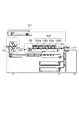
・画像形成装置全体の構成
本実施例における電子写真方式の画像形成装置について簡単に説明する。図1に装置全体の構成を示す。本画像形成装置は、スキャナ部101、露光ヘッド106(106a、106b、106c、106d)、感光ドラム102、定着部104、中間転写体105、および、図4に示される各部から構成される。スキャナ部101は、原稿台に置かれた原稿に対して、照明を当てて原稿画像を光学的に読み取り(スキャンし)、その像を電気信号に変換して画像データを作成する。画像データが作成されると、スキャナ部101は、この画像データを図4に示されるデータ入力部404に入力すると共に、スキャン終了の合図を後述する制御部に対して行う。その後、図4で説明する様々な処理が行われた上で、その画像データ(ディザ処理結果)が電気信号として露光ヘッド106に送られる。すると、露光ヘッド106は、前記画像データ(ディザ処理結果)に応じて発光し、発光した光はロッドレンズアレイによって、感光ドラム102に集光される。なお、露光ヘッド106の詳細構成に関しては後述する。感光ドラム102は、露光ヘッド106による集光前に不図示の帯電器によって帯電されている。前記画像データ(ディザ処理結果)は、ロッドレンズアレイによる集光によって、回転する感光ドラム102に潜像として形成される。感光ドラム102に形成された潜像はトナーにより現像が行われ、その後、トナー像は中間転写体105上に転写される。前記中間転写体105上に転写されたそのトナー像は、不図示の給紙部より給紙される印刷用紙上に転写される。定着部104は、ローラやベルトの組み合わせによって構成され、トナー像が転写された印刷用紙上のトナーを、熱と圧力によって溶解、定着させる。定着された印刷用紙は不図示の搬送部を介して出力され、画像形成装置の印刷動作が完了する。
-Overall Configuration of Image Forming Apparatus The electrophotographic image forming apparatus in this embodiment will be briefly described. FIG. 1 shows the overall configuration of the apparatus. The image forming apparatus includes a
・露光ヘッドの構成
本実施例では露光ヘッド106によって、感光体ドラム102に露光を行う。図2(a)は、画像形成装置における感光ドラム102と露光ヘッド106の配置を示すものである。また、図2(b)は図2(a)の中央位置の断面図を示しており、露光ヘッド106含まれる発光素子から発せられる光が感光ドラム102に対して集光される様子を示している。なお、露光ヘッド106、および感光体ドラム102は、不図示の取り付け部材によって、各々、画像形成装置に取り付けられている。
図2(b)において、露光ヘッド106は、発光素子群1061と、発光素子群1061が配置されたプリント基板1062、ロッドレンズアレイ1063、ロッドレンズアレイ1063とプリント基板1062を取り付けるハウジング1064で構成されている。ハウジング1064は、プリント基板1062とロッドレンズアレイ1063を画像形成装置に対して固定するものであり、感光体ドラム102を支える部材に取り付けられる。ここで、感光体ドラム102とロッドレンズアレイ1063の間の距離、ロッドレンズアレイ1063と発光素子群1061の間の距離は、等間隔となるように配置されることで、発光素子群1061の光が感光体ドラム102上に結像される。なお、1061を発光素子群として説明を行ったが、本図面上は、この発光素子群のうちの1つの発光素子だけが見えている。
In the present embodiment, the
2B, the
図3は、発光素子群1061が配列されたプリント基板1062を、感光ドラム102からみた場合の図(ロッドレンズアレイ1063、ハウジング1064を除いた図)である。なお、同図において、図2で説明した構成と同一のものに関しては、同じ符号を付与している。図3において、発光素子群1061における各発光素子は、感光ドラムの長手方向(以下、主走査方向)に等間隔に配置されている。1061−1から1061−nのそれぞれは、発光素子を表した、発光素子群1061の一部拡大図である。主走査方向の解像度が1200dpiの場合、画素間の間隔は略21.1μmであるため、発光素子1061−1と発光素子1061−2の間隔D1は略21.1μmとなっている。露光ヘッド106の印字幅は、画像形成装置の印字対象とする紙サイズによって決定する。例えば、A3 1200dpiに対応した画像形成装置において、nは15,000画素程度に相当するため、約15,000の発光素子がプリント基板1062上に構成される。なお、本実施例におけるnは、画像形成装置が対応する印字幅に相当する発光素子の数となっており、その数に比べて過剰に多い数とはなっていない。
FIG. 3 is a view when the printed
・画像形成装置(印刷装置)の制御部の構成
本実施例における画像形成装置の制御部、ハーフトーン処理部等の構成に関して説明する。図4は、画像形成装置の構成を示すブロック図である。なお、図4においても、別図に構成した処理部と同じものに関しては同一の符号を付与している。同図において、401は画像形成装置全体を制御するCPU(Central Processing Unit)、402はCPU401の制御プログラムを記憶するROM(Read Only Memory。)、403は、CPU401あるいは後述する各処理部により処理された画像データを一時記憶するメモリである。本実施例における画像形成装置の制御部は、前記CPU401、ROM402およびメモリ403により構成される。
Configuration of control unit of image forming apparatus (printing apparatus) The configuration of a control unit, a halftone processing unit, and the like of the image forming apparatus in this embodiment will be described. FIG. 4 is a block diagram illustrating a configuration of the image forming apparatus. Note that, in FIG. 4 as well, the same reference numerals are assigned to the same processing units as those shown in another figure. In the figure, 401 is a CPU (Central Processing Unit) that controls the entire image forming apparatus, 402 is a ROM (Read Only Memory) that stores a control program of the
404はデータ入力部であり、ここには、スキャナ部101により読み取られた画像データ(あるいはPCから入力された画像データでも良い)が入力される。このデータ入力部404は、入力画像データの変換機能を含むものとする。この変換機能により、入力された画像データ(通常は、RGB各8bitの輝度データ)がCMYK濃度データ(CMYK各8bitの濃度データ)に変換される。
405は、ハーフトーン処理部であり、データ入力部404を介して入力された濃度データに対して、ハーフトーン処理を行う。なお、ハーフトーン処理結果には、画素毎の処理結果(1又は0)が含まれる。
このハーフトーン処理405により実施されるハーフトーン処理にディザ処理がある。このディザ処理時の制御について、詳細は後述するが、ハーフトーン処理結果は、電気信号の形態で駆動部1065へと渡される。
The halftone processing performed by the
なお、データ入力部404もハーフトーン処理部405もハードウェアにより構成されているものとする。なお、このディザ処理結果が電気信号として露光ヘッド106に送られることになる。
It is assumed that both the
・画像データと発光素子群の関係および点灯制御
図5に、ハーフトーン処理結果と、露光ヘッド106に構成した発光素子群との関係を表すブロック図を示す。プリント基板1062には、発光素子群1061(個々の発光素子は発光素子1061−1〜発光素子1061−n)と、発光素子を個別に駆動する駆動部1065が実装されている。前記駆動部1065には、501を介して、ハーフトーン処理部405によって生成される画像データ(ハーフトーン処理結果)が電気信号の形態で渡される。例えば、ハーフトーン処理結果の主走査方向に伸びる1ライン全てが1の場合、駆動部1065は、接続されている発光素子を全て点灯するように制御する。あるいは、ハーフトーン処理結果の先頭の2画素のみが1で他の画素が0である場合、駆動部1065は、発光素子1061−1、および発光素子1061−2のみを点灯するように制御する。このように、露光ヘッド106は、入力される画像データ(ハーフトーン処理結果)に基づき、そのハーフトーン処理結果で1となる画素に該当する主走査方向位置に存在する発光素子のみを発光する。
FIG. 5 is a block diagram showing the relationship between the halftone processing result and the light emitting element group configured in the
・ディザ処理
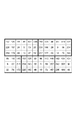
次に本実施例の特徴であるディザ処理に関して説明する。図6にカラー画像データを形成するうちのブラック(K)に関するディザマトリクスの構成を示す。なお、本実施例の説明においては、単色に関するディザマトリクスを対象とするが、本実施例の形態を他の色、すなわち、シアン(C)、マゼンタ(M)、イエロー(Y)に対しても、同じように適用するものとする。図6は、本実施例のディザ処理で用いられるディザマトリクス(係数配列、即ち、閾値配列)を示すものであるが、他のディザマトリクスであっても構わない。なお、図6における太枠は便宜上のもので無視して頂いて構わない。また、このディザマトリクスは、6×12+1=73階調を表現する際に用いられるディザマトリクスであるが、256階調を表現できるディザマトリクスの方が好ましいのは言うまでも無い。
Dither processing Next, dither processing, which is a feature of this embodiment, will be described. FIG. 6 shows the configuration of a dither matrix for black (K) in forming color image data. In the description of this embodiment, a dither matrix relating to a single color is targeted. However, the embodiment is applied to other colors, that is, cyan (C), magenta (M), and yellow (Y). Shall apply in the same way. FIG. 6 shows a dither matrix (coefficient array, that is, threshold array) used in the dither processing of the present embodiment, but other dither matrices may be used. The thick frame in FIG. 6 is for convenience and can be ignored. Further, this dither matrix is a dither matrix used when expressing 6 × 12 + 1 = 73 gradations, but it is needless to say that a dither matrix capable of expressing 256 gradations is preferable.
ディザ処理は、ディザマトリクス(即ち、各係数)とデータ入力部404を介して入力される画像データ(即ち、各画素の濃度データ)との比較によって、その画像データをN値化する処理である。本実施例においては、Nを2(結果は0あるいは1を出力)として説明する。具体的には、データ入力部404から入力される濃度データ(値が小さいほど明るい)が、その濃度データを持つ画素に対応する位置に存在するディザマトリクス係数を下回る場合にハーフトーン処理部405は0(発光素子非点灯。)を、それ以外の場合に1(発光素子点灯)を出力する。図7(a)、図7(b)にデータ入力部404から入力された濃度データに対するディザ処理の結果を示す。図7(a)は、データ入力部404から入力される濃度データが、一様に13(値域の約5%:ハイライト)である場合のディザ処理後の結果を示し、ディザ処理の結果として1となるディザマトリクス係数箇所に網掛け表示を施している。同図からわかるように、図6(b)のディザマトリクス係数との比較によって1が出力される位置は12画素×6画素を単位として4箇所(ディザマトリクス係数0,3,6,9の位置)となる。したがって、この場合の発光素子は、主走査方向に構成した発光素子群のうち12画素を単位として、1画素目、4画素目、7画素目、10画素目に対応する位置に存在する発光素子が発光する。本ディザ処理は、ディザマトリクスを、画像データにおける最も左上の画素(即ち、主走査方向、副走査方向共に先頭の画素。)を含む主走査方向に12画素×副走査方向に6画素の画素群に適用した後、今度は、最も上のラインにおける左から13番目の画素(即ち、主走査方向に13番目の画素、副走査方向に先頭の画素。)を含む12画素×6画素の画素群に同じディザマトリクスを適用する。このように、ディザマトリクスを縦6画素、横12画素の周期で画像データに適用されるため、最も左上の画素から見て主走査方向における13画素目、16画素目、19画素目...のように周期的に点灯対象の発光素子が決まる。つまり、1画素目から3画素位置毎に発光素子が点灯することになる。次に図7(b)は、データ入力部404から入力される画像データが一様に26(値域の約10%:ハイライト)である場合のディザ処理結果を示す。同図からわかるように、図6(b)のディザマトリクス係数との比較によって1が出力される位置は12画素×6画素を単位として8箇所(ディザマトリクス係数0,3,6,9,13,16,19,22の位置)となる。したがって、この場合の発光素子においても、主走査方向に構成した発光素子群のうち12画素を単位として、1画素目から3画素位置毎に該当する発光素子が発光する。
The dither process is a process for converting the image data into N values by comparing the dither matrix (that is, each coefficient) with the image data (that is, the density data of each pixel) input via the
・ディザマトリクスの変更
図7(a)および図7(b)によれば、入力画像データが、低濃度(ハイライト部)で構成される場合、ディザマトリクスの構成サイズを単位に主走査方向に同一の位置のディザ処理後の結果が1となる。ディザ処理後の結果は、露光ヘッド106に構成されているプリント基板1062の駆動部1065による点灯制御に繋がる。したがって、画像形成装置によって印刷する画像データが、一様に低濃度(ハイライト部)である場合、点灯する発光素子は常に同じ位置となる。オフィスにおいて印刷する画像データは、低濃度部(ハイライト部)を下地として、高濃度の文字が構成される場合が多いため、このような低濃度で構成される画像データの頻度は高い。したがって、印刷時、主走査方向同位置の発光素子が点灯する頻度が非常に高くなる。点灯する発光素子の偏りは、該当する発光素子の寿命を短くするだけでなく、発光素子が欠落する前の段階であっても光量の変動により印刷画像データの画質劣化につながる。したがって、本実施例は、ディザ処理に用いるディザマトリクスの基準位置を、主走査方向に所定分ずらす処理を施す。以下、この処理に関して詳細に説明する。
Change of Dither Matrix According to FIGS. 7A and 7B, when the input image data is composed of a low density (highlight portion), the dither matrix is configured in the main scanning direction in units of the configuration size. The result after dithering at the same position is 1. The result after the dither processing leads to lighting control by the
図8(a)は図6(b)に示したディザマトリクスの位相を1画素分ずらしたものである。ディザマトリクス係数:147の位置を基準位置とすると、この基準位置が主走査方向(右方向)に1画素分ずれていることがわかる。基準位置が1画素分ずれているため、図6(b)における右端のディザマトリクス係数が左端に存在されている。この構成のディザマトリクスを用い、一様に13(値域の約5%:ハイライト)である画像データに対してディザ処理を実施した結果を図9(a)に示す。また、同様に、一様に26(値域の約10%:ハイライト)である画像データに対してディザ処理を実施した結果を図9(b)に示す。適用するディザマトリクスの基準位置を1画素分シフトしているため、図9(a)、図9(b)に示した発光素子位置は、図7(a)、図7(b)に対して、基準位置をずらした方向に1画素分シフトする。
FIG. 8A shows the phase of the dither matrix shown in FIG. 6B shifted by one pixel. If the position of the
また、図8(b)は図6(b)に示したディザマトリクスの周期を主走査方向(右方向)に2画素分ずらしたものである。基準位置を2画素分ずらしているため、図6(b)における右端2列のディザマトリクス係数が左端側2列として構成されている。この構成のディザマトリクスを用い、一様に13(値域の約5%:ハイライト)である画像データに対してディザ処理結果を図10(a)に示す。また、同様に、一様に26(値域の約10%:ハイライト)である画像データに対してディザ処理を実施した結果を図10(b)に示す。適用するディザマトリクスの基準位置を2画素分シフトしているため、図10(a)、図10(b)に示した、発光する素子の位置は、図7(a)、図7(b)に対して、2シフトする。 FIG. 8B is a diagram in which the period of the dither matrix shown in FIG. 6B is shifted by two pixels in the main scanning direction (right direction). Since the reference position is shifted by two pixels, the dither matrix coefficients in the rightmost two columns in FIG. 6B are configured as the two leftmost columns. FIG. 10A shows a dither processing result for image data that is uniformly 13 (about 5% of the range: highlight) using the dither matrix having this configuration. Similarly, FIG. 10B shows the result of dithering the image data that is uniformly 26 (about 10% of the range: highlight). Since the reference position of the dither matrix to be applied is shifted by two pixels, the positions of the light emitting elements shown in FIGS. 10 (a) and 10 (b) are as shown in FIGS. 7 (a) and 7 (b). 2 shifts.
つまり、低濃度部(即ち、ハイライト部。)を多く含む画像データを続けて印刷する場合、ハーフトーン処理部405のディザ処理に用いるディザマトリクスの位相をシフトすることで、露光ヘッド106に構成したプリント基板1062の点灯する発光素子をずらすことが可能となる。以下、別図を用い、前記発光素子位置変更に関する制御部の制御に関して説明する
図11は、ハーフトーン処理部405のディザ処理で使用されるディザマトリクスの基準位置変更に関する制御部の制御フローを説明する図である。
That is, when continuously printing image data including a large amount of low density portions (that is, highlight portions), the
制御部は、スキャン終了の合図を受けると、制御部内に保持された、ハーフトーン処理部405による直前のディザ処理で適用されたディザマトリクスの読み取りを行う(ステップS101)。なお、画像形成装置の初期状態においては、制御部内に保持されているディザマトリクスの基準位置は、ずらされていないものを適用するものとする。 When the control unit receives a signal indicating the end of scanning, the control unit reads the dither matrix that is held in the control unit and applied in the immediately preceding dither process by the halftone processing unit 405 (step S101). In the initial state of the image forming apparatus, the reference position of the dither matrix held in the control unit is not shifted.
次に、制御部は、読み取ったディザマトリクス内の係数の位相を横方向(主走査方向)に変更し、変更された後のディザマトリクスをハーフトーン処理部405に設定する(ステップS102)。なお、ステップS102において実施する変更は、ディザマトリクス内の基準位置(147の閾値の位置)が変更されうるものであれば如何なるものでも良い。例えば、ディザマトリクスの基準位置を右側にK(Kは、1以上、ディザマトリクスの主走査方向の長さ−1以下の値である必要がある。今回の例では、1以上11以下となる)シフトする方式でも良いし、1以上11以下の値域で乱数値を生成させ、生成した乱数値分、ディザマトリクスの基準位置を右側にずらす構成にしても良い。いずれの場合においても、プリント基板1062上に配置された各発光素子(1061−1〜1061−n)の連続点灯を極力避けられることになる。つまり、ディザ処理に適用されるディザマトリクス係数と、低濃度部(ハイライト部)の画像データの値を考慮し、点灯される発光素子が、印刷実施時に変わるための演算を行う。したがって、制御部によるステップS102の制御を、画像形成装置における印刷ページ、あるいはジョブを単位に実施するようにする。なお、ディザマトリクスの基準位置を右側にK、シフトした場合、Kの列分の係数がディザマトリクスの右側にはみ出ることになるが、これらの係数は、ディザマトリクスの左側に収納されることになる。よって、このシフトが行われたとしても、シフト前のディザマトリクスとシフト後のディザマトリクスの持つサイズ(係数の数。今回の例では、12×6=72)や、夫々のディザマトリクスに含まれる係数は同じとなる。
Next, the control unit changes the phase of the coefficient in the read dither matrix in the horizontal direction (main scanning direction), and sets the changed dither matrix in the halftone processing unit 405 (step S102). The change performed in step S102 may be any change as long as the reference position (the threshold position of 147) in the dither matrix can be changed. For example, the reference position of the dither matrix is K on the right side (K must be 1 or more and the length of the dither matrix in the main scanning direction minus 1 or less. In this example, it is 1 or more and 11 or less) A shift method may be used, or a random value may be generated in a range of 1 to 11, and the reference position of the dither matrix may be shifted to the right by the generated random value. In any case, continuous lighting of the light emitting elements (1061-1 to 1061-n) arranged on the printed
制御部は、ステップS102により、ディザマトリクスの基準位置設定を実施すると、以下の制御を実施する(ステップS103)。具体的には、データ入力部404から入力された画像データを、制御部内に記憶させる。そして、制御部内部に記憶された画像データを、ハーフトーン処理部405に転送する。すると、ハーフトーン処理部405は、制御部の制御に基づき転送される画像データに対し、設定されたディザマトリクスを適用する。ディザ処理が終了すると、ハーフトーン処理部405は制御部に連絡する。すると、制御部は、ハーフトーン処理部405に、生成された画像データ(ハーフトーン処理結果)を露光ヘッド106に電気信号として転送させる。
When the control unit sets the dither matrix reference position in step S102, the control unit performs the following control (step S103). Specifically, the image data input from the
制御部は、データ入力部404から入力される全ての画像データの処理が終了するまでS103の処理を繰り返す(ステップS104)。制御部は、データ入力部404から入力される全画像データが、ハーフトーン処理部405によりディザ処理されたことを確認すると(ステップS104のYes。)、ハーフトーン処理部405のディザ処理に適用されたディザマトリクスの基準位置を制御部内部に保持する(ステップS105)。なお、露光ヘッド106により露光された画像データは、感光ドラム102に潜像として形成される。そして、感光ドラム102に形成された潜像に、トナーが付着することによって現像が行われる。現像された画像データは中間転写体105上に転写され、転写された画像データは、定着部104によって、搬送部から搬送される印刷用紙に構成され、印刷物として画像形成装置から出力される。
The control unit repeats the process of S103 until the processing of all the image data input from the
以上、説明したように、本発明の第1実施例においては、画像形成装置における印刷時、ディザ処理時に適用するディザマトリクス内の係数の位相を主走査方向にずらすことによって、低濃度(ハイライト部。)で構成される画像データ印刷時の発光素子の連続点灯頻度を低減することが可能となる。また、ディザマトリクスの変更を行うタイミングをページ毎にすることによって、同一画像データの連続印刷時においても、同一発光素子の連続点灯頻度を減らすことが可能となる。 As described above, in the first embodiment of the present invention, the low density (highlight) is achieved by shifting the phase of the coefficient in the dither matrix applied at the time of printing and dither processing in the image forming apparatus in the main scanning direction. Part)), it is possible to reduce the frequency of continuous lighting of the light emitting elements when printing image data. In addition, by changing the timing for changing the dither matrix for each page, it is possible to reduce the frequency of continuous lighting of the same light emitting element even during continuous printing of the same image data.
また、今回の例では、ディザマトリクス内の係数の位相をずらすことにより、新しいディザマトリクスを生成し、これを画像データに適用したが、必ずしも、この方法でなくても良い。例えば、ディザマトリクス内の係数は変えず(即ち、ディザマトリクス自体は変えず)、ディザマトリクスを適用する際の位相をずらしても良い。即ち、左上の画素から始まる12画素×6画素にディザマトリクスを適用するのではなく、左上の画素を含む計6画素のラインには、12画素×6画素のディザマトリクスのうちの右端6画素の係数を適用する。そして、左から2番目で、かつ、最も上の画素から始まる12画素×6画素にディザマトリクスを適用するような形態であっても良い。 In this example, a new dither matrix is generated by shifting the phase of the coefficients in the dither matrix and applied to the image data. However, this method is not necessarily required. For example, the phase in applying the dither matrix may be shifted without changing the coefficients in the dither matrix (that is, without changing the dither matrix itself). That is, the dither matrix is not applied to the 12 pixels × 6 pixels starting from the upper left pixel, but the 6 pixels line including the upper left pixel has 6 pixels on the right edge of the 12 pixel × 6 pixel dither matrix. Apply coefficients. The dither matrix may be applied to 12 pixels × 6 pixels that are second from the left and start from the top pixel.
また、S101、S102の処理は、ページ毎に必ず行うのではなく、ジョブ毎に行っても良い。つまり、同じジョブ内(例えば、10枚の用紙が連続的にスキャンされ、2部印刷の設定がされている場合には、20枚分の印刷が同じジョブとなる。)の場合には、同じ位相で(あるいは同じ位相を持った)ディザマトリクスを適用し、違うジョブが始まる際に、ディザマトリクスの位相(あるいはディザマトリクスを適用する位相)をずらしても良い。 Further, the processing of S101 and S102 is not necessarily performed for each page but may be performed for each job. That is, in the same job (for example, when 10 sheets are continuously scanned and printing of two copies is set, printing for 20 sheets is the same job). A dither matrix may be applied in phase (or having the same phase), and the phase of the dither matrix (or the phase to which the dither matrix is applied) may be shifted when a different job starts.
[第2実施例]
第1実施例においては、画像形成装置における印刷時、ページあるいはジョブを単位として、ディザマトリクスの基準位置をシフトする構成に関して説明した。しかし、低濃度部(ハイライト部)を多く含まない画像データを印刷する場合、プリント基板1062に構成した、各発光素子(1061−1〜1061−n)は画像データに基づき、固定状態での点灯とはならない。つまり、このような画像データの印刷を実施した後においては、ディザマトリクスの基準位置を変更する制御を行う必要はない。以降、本発明の第2実施形態として、この場合のハーフトーン処理部405の動作と制御部の制御に関して説明する。
[Second Embodiment]
In the first embodiment, the configuration in which the reference position of the dither matrix is shifted in units of pages or jobs during printing in the image forming apparatus has been described. However, when printing image data that does not include many low density portions (highlight portions), the light emitting elements (1061-1 to 1061-n) configured on the printed
・ハーフトーン処理部の動作フロー
図12は、ハーフトーン処理部405の動作を示すフローである。ハーフトーン処理部405は、制御部の制御に基づき、データ入力部404を介して入力される画像データに対してディザ処理を実施するが、その処理開始前において、ハーフトーン処理部405内部に構成した不図示のカウンタを初期化する(ステップS201)。ハーフトーン処理部405は、画像データが入力されると、入力された画像データが第1の閾値以下であるかを確認する(ステップS202のYes,ステップS203)。この第1の閾値は、制御部により、データ入力部404から入力される画像データの濃度を判定する値が設定される。なお、ハーフトーン処理部405は、画像データが入力されるまでは、ディザ処理を行わずに画像データの入力を待つ(ステップS202のNo)。入力された画像データが第1の閾値以下、すなわち低濃度(ハイライト)の画素データであった場合、画像形成部405はカウンタに対して1を加算する(ステップS203のYes,ステップS204)。ハーフトーン処理部405は、入力された画像データが第1の閾値を超えるものであると判断した場合、カウンタに対する加算処理は行わず、次の画像データを待つ(ステップS203のNo)。なお、前記説明においては、1画素を単位としてカウンタへの加算を実施することを示したが、本実施例はこれに限定されるものではない。つまり、複数画素連続して第1の閾値以下である場合に加算を行うようにしても良いし、主走査方向、副走査方向の所定領域を単位としても良い。
FIG. 12 is a flowchart showing the operation of the
ハーフトーン処理部405は、データ入力部404からの全画像データが入力されるまで、前記ステップS203からステップS204の処理を繰り返し実施する(ステップS205)。ハーフトーン処理部405は、データ入力部404からの全画像データの第1閾値比較処理を終了すると、その時点において保持しているカウンタ値を所定の第2閾値と比較する。この第2閾値は、制御部によりデータ入力部404から入力された、1ページの画像データ中に低濃度の画像データがどれだけ含まれているかを判定する値が設定される。保持したカウンタ値が、第2の閾値よりも大きい場合、データ入力部404から入力された画像データに、多くの低濃度(ハイライト)画素が含まれていたものと判断する。そして、ハーフトーン処理部405内部に構成した不図示のディザマトリクスの基準位置変更フラグを有効に設定する(ステップS206のYes、ステップS207)。なお、保持したカウンタ値が、第2の閾値よりも小さい場合、データ入力部404から入力された画像データに、低濃度(ハイライト)画素はあまり含まれていないと判断し、ディザマトリクスの基準位置変更フラグを無効に設定する(ステップS208)。
The
・制御部の制御フロー
次にハーフトーン処理部405が図12に基づく処理を実施した場合の制御部の制御に関して説明する。図13は、第2実施例における制御部の制御フローを示す図である。制御部は、データ入力部404から入力される画像データに対するディザ処理開始制御前に、ハーフトーン処理部405に構成されている基準位置変更フラグの状態を確認する。ハーフトーン処理部405に保持されたディザマトリクスの基準位置変更フラグが有効を示すものであった場合、直前に処理された画像データには多くの低濃度(ハイライト)画素が含まれていたものと判断する(ステップS301のYes)。この場合、第1実施例における制御と同様に、メモリ403に保持されているディザマトリクス基準位置を読み取る(ステップS302)。そして、発光素子の連続点灯を低減させるため、ハーフトーン処理部405に対して設定するディザマトリクス基準位置を、保持されていた基準位置とは別のものとして設定を行う(ステップS303)。なお、ハーフトーン処理部405に保持されたディザマトリクスの基準位置変更フラグが無効であった場合は、直前に処理された画像データには多くの低濃度(ハイライト)画素が含まれていないものと判断する。この場合、直前の印刷において、プリント基板1062に構成した発光素子群1061の点灯位置が固定化されていないものと判断し、ハーフトーン処理部405に対するディザマトリクスの基準位置の変更は行わないように制御する(ステップS301のNo)。
Control Flow of Control Unit Next, control of the control unit when the
以上、説明したように、第2実施例においては、直前の印刷画像データの状態に応じて、ディザマトリクスの基準位置を変更するか否かを制御出来る。これにより、点灯する発光素子が固定とならない画像データの印刷実施後に、ディザマトリクスの基準位置を変更することがなくなり、より適正に発光素子の連続点灯を低減させる制御を実現出来る。 As described above, in the second embodiment, whether or not to change the reference position of the dither matrix can be controlled in accordance with the state of the previous print image data. This eliminates the need to change the reference position of the dither matrix after printing of image data in which the light emitting elements to be lit are not fixed, and it is possible to realize control that more appropriately reduces the continuous lighting of the light emitting elements.
[第3実施例]
第1実施例においては、露光ヘッド106のプリント基板1062に構成された発光素子群1061が主走査方向に一列で構成されていたものに関して説明を行った。しかし、発光素子に有機ELを適用する場合、プリント基板に対して発光面を印刷するため、発光素子群1061を複数列構成することが容易である。このため、第3実施例においては、発光素子群1061が複数列構成された場合に関する制御に関して説明する。
[Third embodiment]
In the first embodiment, a description has been given of the case where the light emitting
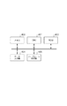
・発光素子群の複数構成
図14に、露光ヘッド106として、発光素子群を2列とした場合の構成図を示す。同図において、図3と同じ構成であるものに関しては、同一符号を付与している。図14において、図3と異なる点はプリント基板1062に対して、発光素子群が2列構成されていることである。すなわち、図3に示した発光素子群1061に対して、同一解像度の第2の発光素子群1061’が構成されている。発光素子群1061および発光素子群1061’は同一解像度であるため、発光素子間の距離D1は発光素子群で違いはない。
Multiple Configurations of Light-Emitting Element Group FIG. 14 shows a configuration diagram when the light-emitting element groups are arranged in two rows as the
・ディザマトリクスの基準位置の主副変更
このように2列の発光素子群を構成した露光ヘッドの使途の一例として、レーザービームをポリゴンモータで偏光走査するレーザ走査方式における2ビームに対応させる場合がある。つまり、第1列の発光素子群1061を、印刷する画像データの奇数ラインの露光に使用し、第2列の発光素子群1061’を印刷する画像データの偶数ラインの露光に使用する。このような構成の場合、既に説明したディザマトリクスの基準位置のずらし方向に多用性をもたせることが可能となる。つまり、ディザマトリクスの基準位置を主走査方向にずらすだけでなく、副走査方向に対してもずらすことが出来る。図15に、図6(b)で示したディザマトリクスを主走査方向(右方向)に1、副走査方向(下方向)に1ずらしたディザマトリクスを示す。主走査方向に1ずらしているため、図6(b)の右端のディザマトリクス係数が左端に構成されている。また、主走査方向にずらしたディザマトリクスを基準に下端のディザマトリクス係数が上端のディザマトリクス係数として構成されている。
-Main / sub change of the reference position of the dither matrix As an example of the use of the exposure head comprising two rows of light emitting element groups as described above, there is a case where the laser beam is made to correspond to two beams in a laser scanning method in which a polygon motor scans polarized light. is there. That is, the first row of light emitting
図15で示したディザマトリクスを用いて、一様に13(値域の約5%:ハイライト)である画像データに対してディザ処理を実施した結果を図16(a)に示す。また、同様に、一様に26(値域の約10%:ハイライト)である画像データに対してディザ処理を実施した結果を図16(b)に示す。図16(a)においては、適用するディザマトリクスの基準位置を主走査方向に1画素分シフトしているため、図16(a)の発光素子位置は図7(a)に対して、主走査方向(右方向)に1画素分シフトされている。しかし、第3実施例においては、発光素子群が2列存在し、奇数ラインと偶数ラインで使用する発光素子群を変えている。このため、主走査方向12画素、副走査方向6画素を単位とすると、第1列の発光素子位置としては、第5画素目、第11画素目となる。また、第2列の発光素子位置としては、第2画素目、第8画素目となる。同様に、図16(b)の発光素子位置に関しても図7(b)に対して、主走査方向(右方向)に1画素分シフトされている。この場合も奇数ラインと偶数ラインで使用する発光素子群を変えているため、主走査方向12画素、副走査方向6画素を単位とすると、第1列の発光素子位置および第2列の発光素子位置は、第2画素目、第5画素目、第8画素目、第11画素目となる。このとき、第1列と第2列の発光素子位置は同一となるが、発光素子の点灯頻度の観点においては1列の発光素子群で構成した場合の結果である図7(b)よりも低減させている。 FIG. 16A shows the result of dithering the image data uniformly 13 (about 5% of the range: highlight) using the dither matrix shown in FIG. Similarly, FIG. 16B shows the result of dithering the image data that is uniformly 26 (about 10% of the range: highlight). In FIG. 16A, since the reference position of the dither matrix to be applied is shifted by one pixel in the main scanning direction, the light emitting element position in FIG. 16A is in the main scanning direction with respect to FIG. It is shifted by one pixel in the direction (right direction). However, in the third embodiment, there are two rows of light emitting element groups, and the light emitting element groups used in odd lines and even lines are changed. Therefore, when the main scanning direction is 12 pixels and the sub-scanning direction is 6 pixels, the light emitting element positions in the first column are the fifth pixel and the eleventh pixel. The light emitting element positions in the second column are the second pixel and the eighth pixel. Similarly, the light emitting element position in FIG. 16B is also shifted by one pixel in the main scanning direction (right direction) with respect to FIG. 7B. Also in this case, since the light emitting element groups used in the odd lines and the even lines are changed, if the unit is 12 pixels in the main scanning direction and 6 pixels in the sub scanning direction, the light emitting element positions in the first row and the light emitting elements in the second row are used. The positions are the second pixel, the fifth pixel, the eighth pixel, and the eleventh pixel. At this time, the positions of the light emitting elements in the first row and the second row are the same, but from the viewpoint of the lighting frequency of the light emitting elements, the result of the case where the light emitting elements are composed of one row is more than that shown in FIG. It is reduced.
このように、露光ヘッド106に発光素子列を複数列構成した場合においては、ハーフトーン処理部405のディザ処理におけるディザマトリクス基準位置を主走査方向だけでなく、副走査方向にもずらすことが可能となる。したがって、露光ヘッド106に構成した発光素子群の列数、ディザ処理におけるサブマトリクスの構成、あるいはライン成長させる角度に応じ、ディザマトリクスの基準位置を変更することで発光素子の連続点灯あるいは連続点灯頻度を低減させることが可能となる。
As described above, when a plurality of light emitting element arrays are formed in the
なお、第3実施例においても、第2実施例で説明した制御を実施しても良い。すなわち、ハーフトーン処理部405に入力された画像データに応じて、ディザマトリクスの基準位置をずらすか否かを決定しても良い。更に、ハーフトーン処理部405に入力された画像データに応じて、主走査方向と副走査方向に独立のずらし値を適用させるように構成しても良い。
In the third embodiment, the control described in the second embodiment may be performed. That is, whether or not to shift the reference position of the dither matrix may be determined according to the image data input to the
[他の実施例]
以上、発光素子の場合を例に説明したが、インクジェットのインク途出素子のように、1画素あたり1素子又は複数素子の構成を取っている印刷装置でも同じ問題が発生する。よってそうした印刷装置も本フローチャートを具備することは好ましい。また、本問題を解決しなくてはいけないのは印刷装置に限られない。例えば、印刷は必ずしも実行するとは限らないが、ディザ処理可能なアプリケーション(例えば、PHOTOSHOP(登録商標))のインストールされたホストコンピュータでも、こうしたフローチャートを具備するのは好ましいのは言うまでもない。なぜなら、そうしたアプリケーションで得られたディザ処理結果(ディザ処理の適用結果)が、そうした印刷素子を持つ印刷装置に送られることは往々にしてあるからである。
[Other embodiments]
As described above, the case of the light emitting element has been described as an example, but the same problem occurs even in a printing apparatus having a configuration of one element or a plurality of elements per pixel, such as an ink-jet ink leaving element. Therefore, it is preferable that such a printing apparatus also includes this flowchart. Further, it is not limited to a printing apparatus that has to solve this problem. For example, although printing is not always executed, it is needless to say that a host computer on which an application capable of dither processing (for example, PHOTOOSOP (registered trademark)) is installed also includes such a flowchart. This is because the dither processing result obtained by such an application (the application result of the dither processing) is often sent to a printing apparatus having such a printing element.
なお、発光素子やインク途出素子のように印刷に利用される素子のことを印刷素子と本明細書では呼ぶことにする。 Note that an element used for printing such as a light emitting element or an ink leakage element is called a printing element in this specification.
また、本発明は、以下の処理を実行することによっても実現される。即ち、上述した実施形態の機能を実現するソフトウェア(プログラム)を、ネットワーク又は各種記憶媒体を介してシステム或いは装置に供給し、そのシステム或いは装置のコンピュータ(またはCPUやMPU等)がプログラムを読み出して実行する処理である。 The present invention can also be realized by executing the following processing. That is, software (program) that realizes the functions of the above-described embodiments is supplied to a system or apparatus via a network or various storage media, and a computer (or CPU, MPU, or the like) of the system or apparatus reads the program. It is a process to be executed.
Claims (4)
直前のページの画像データに適用されたディザマトリクスが有する前記複数の閾値の配列における基準位置を示す情報を保持手段に保持する保持工程と、
前記1ページのシートに印刷される画像データにおける画素の濃度と所定の濃度閾値とを比較し、前記濃度閾値以下である画素の数又は前記濃度閾値以下である画素が所定数連続した画素群の数をカウントするカウント工程と、
前記カウント工程におけるカウント結果を表すカウント値と、所定のカウンタ閾値とを比較する比較工程と、を有し、
前記第1のディザマトリクスおよび前記第2のディザマトリクスは、前記主走査方向および前記副走査方向に同じ数の閾値を有し、
前記第1のディザマトリクスは前記保持手段に保持された前記情報が示す前記基準位置を基準とした前記複数の閾値の配列を有するディザマトリクスであり、前記第2のディザマトリクスは前記複数の閾値の配列における基準位置をずらすことにより前記第1のディザマトリクスが有する前記複数の閾値の配列の位相を前記主走査方向にずらしたディザマトリクスであり、
前記比較工程による前記カウント値と前記所定のカウンタ閾値との比較結果が、前記カウント値が前記カウンタ閾値以上であることを示す場合に、前記適用工程において、前記第2のディザマトリクスを前記1ページのシートに印刷される画像データに適用し、前記比較結果が、前記カウント値が前記カウンタ閾値未満であることを示す場合に、前記適用工程において、前記第1のディザマトリクスを前記1ページのシートに印刷される画像データに適用することを特徴とする方法。 The image data to be printed on one page of sheet, having as first dither matrix or Applicable Industrial that apply a second dither matrix having a plurality of thresholds in the main scanning direction and the sub scanning direction, the image processing apparatus A method of controlling ,
A holding step of holding information indicating reference positions in the array of the plurality of thresholds included in the dither matrix applied to the image data of the immediately previous page in a holding unit;
Wherein comparing the density of pixels in the image data to be printed on a sheet of one page and a predetermined concentration threshold, the is less than or equal to the number or the density threshold pixel is below the concentration threshold pixels of a predetermined number of consecutive pixel groups A counting process for counting the number ;
A comparison step of comparing a count value representing a count result in the counting step with a predetermined counter threshold value,
The first dither matrix and the second dither matrix have the same number of thresholds in the main scanning direction and the sub-scanning direction ,
The first dither matrix is a dither matrix having an array of the plurality of threshold values with reference to the reference position indicated by the information held in the holding means, and the second dither matrix is the plurality of threshold values. A dither matrix in which the phase of the array of the plurality of threshold values included in the first dither matrix is shifted in the main scanning direction by shifting a reference position in the array;
Comparison result between the said count value of pre-Symbol comparing step a predetermined counter threshold, to indicate that the count value is equal to or larger than the counter threshold, before Kiteki for step, before Symbol second dither matrix It applied to the image data to be printed on a sheet of the first page, the comparison result, to indicate that the count value is less than the counter threshold value, before Kiteki for step, the first dither matrix Is applied to image data printed on the one-page sheet .
直前のページの画像データに適用されたディザマトリクスが有する前記複数の閾値の配列における基準位置を示す情報を保持する保持手段と、
前記1ページのシートに印刷される画像データにおける画素の濃度と所定の濃度閾値とを比較し、前記濃度閾値以下である画素の数又は前記濃度閾値以下である画素が所定数連続した画素群の数をカウントするカウント手段と、
前記カウント手段におけるカウント結果を表すカウント値と、所定のカウンタ閾値とを比較する比較手段と、を有し、
前記第1のディザマトリクスおよび前記第2のディザマトリクスは、前記主走査方向および前記副走査方向に同じ数の閾値を有し、
前記第1のディザマトリクスは前記保持手段に保持された前記情報が示す前記基準位置を基準とした前記複数の閾値の配列を有するディザマトリクスであり、前記第2のディザマトリクスは前記複数の閾値の配列における基準位置をずらすことにより前記第1のディザマトリクスが有する前記複数の閾値の配列の位相を前記主走査方向にずらしたディザマトリクスであり、
前記比較手段による前記カウント値と前記所定のカウンタ閾値との比較結果が、前記カウント値が前記カウンタ閾値以上であることを示す場合に、前記適用手段は、前記第1のディザマトリクスが有する前記複数の閾値の配列順序の位相を前記主走査方向にずらした前記第2のディザマトリクスを前記1ページのシートに印刷される画像データに適用し、前記比較結果が、前記カウント値が前記カウンタ閾値未満であることを示す場合に、前記適用手段は、前記第1のディザマトリクスを前記1ページのシートに印刷される画像データに適用することを特徴とする画像処理装置。 The image data to be printed on one page of the sheet, the image processing apparatus having a main scanning direction and the first dither matrix or Applicable hand stages that apply the second dither matrix having a plurality of threshold values in the sub-scanning direction There,
Holding means for holding information indicating a reference position in the array of the plurality of threshold values included in the dither matrix applied to the image data of the immediately previous page;
Wherein comparing the density of pixels in the image data to be printed on a sheet of one page and a predetermined concentration threshold, the is less than or equal to the number or the density threshold pixel is below the concentration threshold pixels of a predetermined number of consecutive pixel groups A counting means for counting the number ;
A comparison means for comparing a count value representing a count result in the counting means with a predetermined counter threshold value;
The first dither matrix and the second dither matrix have the same number of thresholds in the main scanning direction and the sub-scanning direction ,
The first dither matrix is a dither matrix having an array of the plurality of threshold values with reference to the reference position indicated by the information held in the holding means, and the second dither matrix is the plurality of threshold values. A dither matrix in which the phase of the array of the plurality of threshold values included in the first dither matrix is shifted in the main scanning direction by shifting a reference position in the array;
Comparison result between the said count value of pre Symbol comparison means a predetermined counter threshold, to indicate that the count value is equal to or larger than the counter threshold, before Kiteki for means, said first dither matrix The second dither matrix in which the phase of the array order of the plurality of threshold values is shifted in the main scanning direction is applied to image data printed on the sheet of one page, and the comparison result indicates that the count value is the count value to indicate that less than the counter threshold value, before Kiteki for means, an image processing apparatus characterized by applying said first dither matrix to the image data to be printed on the sheet of the first page.
Priority Applications (3)
| Application Number | Priority Date | Filing Date | Title |
|---|---|---|---|
| JP2013080804A JP6456013B2 (en) | 2013-04-08 | 2013-04-08 | Apparatus, method, and program for performing dither processing |
| CN201410133327.6A CN104104824B (en) | 2013-04-08 | 2014-04-03 | Method for carrying out dithering process |
| US14/244,731 US9509885B2 (en) | 2013-04-08 | 2014-04-03 | Method for performing dither processing |
Applications Claiming Priority (1)
| Application Number | Priority Date | Filing Date | Title |
|---|---|---|---|
| JP2013080804A JP6456013B2 (en) | 2013-04-08 | 2013-04-08 | Apparatus, method, and program for performing dither processing |
Related Child Applications (1)
| Application Number | Title | Priority Date | Filing Date |
|---|---|---|---|
| JP2018119944A Division JP6608488B2 (en) | 2018-06-25 | 2018-06-25 | Apparatus, method, and program for performing dither processing |
Publications (3)
| Publication Number | Publication Date |
|---|---|
| JP2014201034A JP2014201034A (en) | 2014-10-27 |
| JP2014201034A5 JP2014201034A5 (en) | 2016-06-02 |
| JP6456013B2 true JP6456013B2 (en) | 2019-01-23 |
Family
ID=51654243
Family Applications (1)
| Application Number | Title | Priority Date | Filing Date |
|---|---|---|---|
| JP2013080804A Active JP6456013B2 (en) | 2013-04-08 | 2013-04-08 | Apparatus, method, and program for performing dither processing |
Country Status (3)
| Country | Link |
|---|---|
| US (1) | US9509885B2 (en) |
| JP (1) | JP6456013B2 (en) |
| CN (1) | CN104104824B (en) |
Families Citing this family (5)
| Publication number | Priority date | Publication date | Assignee | Title |
|---|---|---|---|---|
| JP2016130006A (en) * | 2015-01-07 | 2016-07-21 | キヤノン株式会社 | Image processor and control method thereof |
| JP6288040B2 (en) * | 2015-10-30 | 2018-03-07 | コニカミノルタ株式会社 | Optical writing apparatus and image forming apparatus |
| JP6743449B2 (en) * | 2016-03-28 | 2020-08-19 | コニカミノルタ株式会社 | Image forming apparatus, image forming method and control program |
| JP6808414B2 (en) | 2016-09-21 | 2021-01-06 | キヤノン株式会社 | Information processing device, its control method, and program |
| WO2018080520A1 (en) * | 2016-10-28 | 2018-05-03 | Hewlett-Packard Development Company, L.P. | Illumuniation source |
Family Cites Families (13)
| Publication number | Priority date | Publication date | Assignee | Title |
|---|---|---|---|---|
| JPH09275495A (en) * | 1996-04-05 | 1997-10-21 | Toshiba Corp | Document preparing device with image printing function and image printing control method |
| JP2985784B2 (en) * | 1996-07-31 | 1999-12-06 | 日本電気株式会社 | Color image forming apparatus and color misregistration correction method |
| US6278530B1 (en) * | 1998-04-17 | 2001-08-21 | Compaq Computer Corporation | Multi-dimensional dithering using one-dimensional dither arrays |
| JP2002225326A (en) * | 2001-02-05 | 2002-08-14 | Alps Electric Co Ltd | Printing method and printer |
| JP3949931B2 (en) * | 2001-10-30 | 2007-07-25 | 株式会社ルネサステクノロジ | Image forming apparatus |
| JP2004276547A (en) * | 2003-03-19 | 2004-10-07 | Ricoh Co Ltd | Multi-beam image forming apparatus |
| JP2005161817A (en) * | 2003-12-05 | 2005-06-23 | Canon Inc | Method and device for image processing |
| JP2008087196A (en) | 2006-09-29 | 2008-04-17 | Seiko Epson Corp | Optical head driving method, optical head control system, exposure system, and image forming system |
| JP2010122250A (en) * | 2008-11-17 | 2010-06-03 | Seiko Epson Corp | Image forming apparatus and image forming method |
| JP2010120163A (en) * | 2008-11-17 | 2010-06-03 | Seiko Epson Corp | Image forming apparatus and image forming method |
| US20100188678A1 (en) | 2009-01-29 | 2010-07-29 | Canon Kabushiki Kaisha | Image processing apparatus, printing apparatus, and image processing method |
| JP5476874B2 (en) | 2009-09-09 | 2014-04-23 | 富士ゼロックス株式会社 | Color processing apparatus, image forming apparatus, and program |
| JP5055418B2 (en) | 2010-12-10 | 2012-10-24 | キヤノン株式会社 | Image processing apparatus and image processing method |
-
2013
- 2013-04-08 JP JP2013080804A patent/JP6456013B2/en active Active
-
2014
- 2014-04-03 US US14/244,731 patent/US9509885B2/en active Active
- 2014-04-03 CN CN201410133327.6A patent/CN104104824B/en active Active
Also Published As
| Publication number | Publication date |
|---|---|
| CN104104824B (en) | 2017-06-20 |
| US20140300934A1 (en) | 2014-10-09 |
| CN104104824A (en) | 2014-10-15 |
| JP2014201034A (en) | 2014-10-27 |
| US9509885B2 (en) | 2016-11-29 |
Similar Documents
| Publication | Publication Date | Title |
|---|---|---|
| JP6456013B2 (en) | Apparatus, method, and program for performing dither processing | |
| JP2009234116A (en) | Method of calculating correction value and method of discharging liquid | |
| JP2017121782A (en) | Control system, image formation system, control method and control program | |
| JP5223405B2 (en) | Image forming apparatus | |
| JP6171289B2 (en) | Image processing method, image processing apparatus, and program | |
| JP2019077046A (en) | Printer and print control unit | |
| JP6608488B2 (en) | Apparatus, method, and program for performing dither processing | |
| JP6281348B2 (en) | Optical writing apparatus, image forming apparatus, optical writing control method, and program | |
| US8482591B2 (en) | Image forming apparatus for forming latent image on a photosensitive member | |
| JP5744360B1 (en) | Image processing device | |
| JP2017121786A (en) | Control device and computer program | |
| JP4752886B2 (en) | Image forming apparatus and image forming system | |
| US11663432B2 (en) | Printer, non-transitory storage medium storing plurality of instructions, and control method | |
| US11331931B2 (en) | Liquid droplet discharge apparatus | |
| US11951752B2 (en) | Controller, printer, and computer-readable storage medium | |
| JP5471472B2 (en) | Image forming apparatus | |
| JP2005254763A (en) | Image formation device and correction device | |
| JP2006076179A (en) | Printing head, and image forming apparatus | |
| JP2023117207A (en) | Liquid discharge device, liquid discharge method and program | |
| JP5953226B2 (en) | Threshold matrix creation apparatus, method, program, and image forming apparatus | |
| JP2008546351A (en) | Method and system for inter-channel clock frequency selection with periodic halftoning | |
| CN117434805A (en) | Image forming apparatus, control method for controlling image forming apparatus, and storage medium | |
| JP2016124275A (en) | Optical writing control apparatus, image formation device and control method for optical writing | |
| JP2020089985A (en) | Image processing device, control method therefor, and program | |
| JP2010120179A (en) | Image processing apparatus, image processing method and image forming apparatus |
Legal Events
| Date | Code | Title | Description |
|---|---|---|---|
| A521 | Written amendment |
Free format text: JAPANESE INTERMEDIATE CODE: A523 Effective date: 20160405 |
|
| A621 | Written request for application examination |
Free format text: JAPANESE INTERMEDIATE CODE: A621 Effective date: 20160405 |
|
| A977 | Report on retrieval |
Free format text: JAPANESE INTERMEDIATE CODE: A971007 Effective date: 20170308 |
|
| A131 | Notification of reasons for refusal |
Free format text: JAPANESE INTERMEDIATE CODE: A131 Effective date: 20170314 |
|
| A521 | Written amendment |
Free format text: JAPANESE INTERMEDIATE CODE: A523 Effective date: 20170512 |
|
| A02 | Decision of refusal |
Free format text: JAPANESE INTERMEDIATE CODE: A02 Effective date: 20170822 |
|
| A521 | Written amendment |
Free format text: JAPANESE INTERMEDIATE CODE: A523 Effective date: 20171121 |
|
| A911 | Transfer of reconsideration by examiner before appeal (zenchi) |
Free format text: JAPANESE INTERMEDIATE CODE: A911 Effective date: 20171129 |
|
| A912 | Removal of reconsideration by examiner before appeal (zenchi) |
Free format text: JAPANESE INTERMEDIATE CODE: A912 Effective date: 20171222 |
|
| A521 | Written amendment |
Free format text: JAPANESE INTERMEDIATE CODE: A523 Effective date: 20180625 |
|
| A521 | Written amendment |
Free format text: JAPANESE INTERMEDIATE CODE: A523 Effective date: 20181005 |
|
| A61 | First payment of annual fees (during grant procedure) |
Free format text: JAPANESE INTERMEDIATE CODE: A61 Effective date: 20181218 |
|
| R151 | Written notification of patent or utility model registration |
Ref document number: 6456013 Country of ref document: JP Free format text: JAPANESE INTERMEDIATE CODE: R151 |