JP6435617B2 - Atomic cell, quantum interference device, atomic oscillator and electronic equipment - Google Patents
Atomic cell, quantum interference device, atomic oscillator and electronic equipment Download PDFInfo
- Publication number
- JP6435617B2 JP6435617B2 JP2014059250A JP2014059250A JP6435617B2 JP 6435617 B2 JP6435617 B2 JP 6435617B2 JP 2014059250 A JP2014059250 A JP 2014059250A JP 2014059250 A JP2014059250 A JP 2014059250A JP 6435617 B2 JP6435617 B2 JP 6435617B2
- Authority
- JP
- Japan
- Prior art keywords
- metal
- atomic
- liquid
- alkali metal
- cell
- Prior art date
- Legal status (The legal status is an assumption and is not a legal conclusion. Google has not performed a legal analysis and makes no representation as to the accuracy of the status listed.)
- Expired - Fee Related
Links
Images


Classifications
-
- H—ELECTRICITY
- H03—ELECTRONIC CIRCUITRY
- H03L—AUTOMATIC CONTROL, STARTING, SYNCHRONISATION, OR STABILISATION OF GENERATORS OF ELECTRONIC OSCILLATIONS OR PULSES
- H03L7/00—Automatic control of frequency or phase; Synchronisation
- H03L7/26—Automatic control of frequency or phase; Synchronisation using energy levels of molecules, atoms, or subatomic particles as a frequency reference
-
- G—PHYSICS
- G04—HOROLOGY
- G04F—TIME-INTERVAL MEASURING
- G04F5/00—Apparatus for producing preselected time intervals for use as timing standards
- G04F5/14—Apparatus for producing preselected time intervals for use as timing standards using atomic clocks
-
- G—PHYSICS
- G04—HOROLOGY
- G04F—TIME-INTERVAL MEASURING
- G04F5/00—Apparatus for producing preselected time intervals for use as timing standards
- G04F5/14—Apparatus for producing preselected time intervals for use as timing standards using atomic clocks
- G04F5/145—Apparatus for producing preselected time intervals for use as timing standards using atomic clocks using Coherent Population Trapping
-
- H—ELECTRICITY
- H01—ELECTRIC ELEMENTS
- H01S—DEVICES USING THE PROCESS OF LIGHT AMPLIFICATION BY STIMULATED EMISSION OF RADIATION [LASER] TO AMPLIFY OR GENERATE LIGHT; DEVICES USING STIMULATED EMISSION OF ELECTROMAGNETIC RADIATION IN WAVE RANGES OTHER THAN OPTICAL
- H01S1/00—Masers, i.e. devices using stimulated emission of electromagnetic radiation in the microwave range
- H01S1/06—Gaseous, i.e. beam masers
Description
本発明は、原子セル、量子干渉装置、原子発振器および電子機器に関するものである。 The present invention has an atomic cell, quantum interference device, the present invention relates to an atomic oscillator and an electronic equipment.
長期的に高精度な発振特性を有する発振器として、ルビジウム、セシウム等のアルカリ金属の原子のエネルギー遷移に基づいて発振する原子発振器が知られている。 As an oscillator having long-term highly accurate oscillation characteristics, an atomic oscillator that oscillates based on energy transition of an alkali metal atom such as rubidium or cesium is known.
一般に、原子発振器の動作原理は、光およびマイクロ波による二重共鳴現象を利用した方式と、波長の異なる2種類の光による量子干渉効果(CPT:Coherent Population Trapping)を利用した方式とに大別される。 In general, the operating principles of atomic oscillators are broadly divided into methods that use the double resonance phenomenon of light and microwaves, and methods that use the quantum interference effect (CPT: Coherent Population Trapping) of two types of light with different wavelengths. Is done.
いずれの方式の原子発振器においても、通常、アルカリ金属をガスセル(原子セル)内に封入し、そのアルカリ金属を一定のガス状態に保つために、ガスセルをヒーターにより所定温度に加熱する。 In any type of atomic oscillator, an alkali metal is usually enclosed in a gas cell (atomic cell), and the gas cell is heated to a predetermined temperature by a heater in order to keep the alkali metal in a certain gas state.
ここで、一般に、ガスセル内のアルカリ金属は、そのすべてがガス化するのではなく、一部が余剰分として液体となる。このような余剰分のアルカリ金属原子は、ガスセルの温度の低い部分に析出(結露)することにより液体となるが、励起光の通過領域に存在すると、励起光を遮ってしまい、その結果、原子発振器の発振特性の低下を招くこととなる。 Here, in general, all of the alkali metal in the gas cell is not gasified, but a part thereof becomes liquid as a surplus. Such surplus alkali metal atoms become liquid by being deposited (condensation) in the low temperature part of the gas cell, but if they exist in the excitation light passage region, they block the excitation light, and as a result The oscillation characteristics of the oscillator are degraded.
そこで、特許文献1に係るガスセルでは、アルカリ金属を析出させるための凹部がガスセルの内壁面に設けられている。
Therefore, in the gas cell according to
しかし、特許文献1に係るガスセルでは、凹部内に析出した余剰分のアルカリ金属が励起光の通過領域に比較的近くで面した状態で、熱拡散等により状態が時間的に変動しているため、励起されるガス状のアルカリ金属の一部が凹部内の余剰分のアルカリ金属と接触することにより、励起されるガス状のアルカリ金属の状態が不均一となり、その結果、発振特性が低下(例えば周波数変動)するという問題があった。
However, in the gas cell according to
本発明の目的は、余剰分の金属原子による特性の低下を抑制することができる原子セルを提供すること、また、かかる原子セルを備える量子干渉装置、原子発振器および電子機器を提供することにある。 It is an object of the present invention to provide an atomic cell capable of suppressing the deterioration in characteristics due to excess metal atoms, also quantum interference device having such atoms cell, to provide an atomic oscillator and electronic equipment is there.
本発明は、上述の課題の少なくとも一部を解決するためになされたものであり、以下の形態または適用例として実現することが可能である。 SUMMARY An advantage of some aspects of the invention is to solve at least a part of the problems described above, and the invention can be implemented as the following forms or application examples.
[適用例1]
本発明の原子セルは、金属と、
前記金属が封入されている内部空間を構成している壁部と、
を備え、
前記壁部の内壁面は、液体状の前記金属との接触角が90°よりも小さい金属接続部を有することを特徴とする。
[Application Example 1]
The atomic cell of the present invention comprises a metal,
A wall constituting an internal space in which the metal is enclosed;
With
The inner wall surface of the wall portion has a metal connection portion having a contact angle with the liquid metal of less than 90 °.
このような原子セルによれば、液体状の金属に対する金属接続部の濡れ性が高いため、余剰の液体状の金属を金属接続部に濡れ拡がらせて安定的に保持させることができる。そのため、液体状の金属が移動したり振れたりするのを低減すること(すなわち、原子セル内の液体状の金属の挙動を安定化させること)ができ、その結果、余剰分の金属による特性の低下を抑制することができる。 According to such an atomic cell, since the wettability of the metal connection part with respect to the liquid metal is high, the excess liquid metal can be wet-spread on the metal connection part and stably held. Therefore, it is possible to reduce the movement and shake of the liquid metal (that is, to stabilize the behavior of the liquid metal in the atomic cell), and as a result, the characteristic of the excess metal is reduced. The decrease can be suppressed.
[適用例2]
本発明の原子セルでは、前記金属接続部に対する液体状の前記金属の接触角が70°よりも小さいことが好ましい。
これにより、液体状の金属に対する金属接続部の濡れ性を高めることができる。
[Application Example 2]
In the atomic cell of the present invention, it is preferable that a contact angle of the liquid metal with respect to the metal connection portion is smaller than 70 °.
Thereby, the wettability of the metal connection part with respect to a liquid metal can be improved.
[適用例3]
本発明の原子セルでは、前記金属接続部に対する液体状の前記金属の接触角が60°よりも小さいことが好ましい。
これにより、液体状の金属に対する金属接続部の濡れ性をより高めることができる。
[Application Example 3]
In the atomic cell of the present invention, it is preferable that a contact angle of the liquid metal with respect to the metal connection portion is smaller than 60 °.
Thereby, the wettability of the metal connection part with respect to a liquid metal can be improved more.
[適用例4]
本発明の原子セルでは、前記金属の一部が前記内部空間で液体状となっていることが好ましい。
[Application Example 4]
In the atomic cell of the present invention, it is preferable that a part of the metal is in a liquid state in the internal space.
このように液体状の金属が余剰分として内部空間に存在している場合、液体状の金属が移動したり振れたりすると、特性が低下する問題が生じる。したがって、かかる場合に、本発明を適用すると、その効果が顕著に発揮される。 Thus, when the liquid metal exists in the internal space as a surplus, if the liquid metal moves or shakes, there arises a problem that the characteristics deteriorate. Therefore, in such a case, when the present invention is applied, the effect is remarkably exhibited.
[適用例5]
本発明の原子セルでは、前記内部空間は、前記液体状の金属が配置されている金属溜り部を有し、
前記金属接続部は、前記金属溜り部の内壁面に配置されていることが好ましい。
[Application Example 5]
In the atomic cell of the present invention, the internal space has a metal reservoir in which the liquid metal is disposed,
It is preferable that the metal connection portion is disposed on an inner wall surface of the metal reservoir portion.
これにより、原子セルの特性の影響の少ない部位に、液体状の金属を留まらせておくことができる。 Thereby, a liquid metal can be made to stay in the site | part with little influence of the characteristic of an atomic cell.
[適用例6]
本発明の原子セルでは、前記金属接続部の表面粗さRaは、10nm以上980nm以下の範囲内にあることが好ましい。
[Application Example 6]
In the atomic cell of the present invention, it is preferable that the surface roughness Ra of the metal connection portion is in a range of 10 nm or more and 980 nm or less.
これにより、比較的簡単な構成で、余剰の液体状の金属を金属接続部に濡れ拡がらせて安定的に保持させることができる。 Thereby, with a comparatively simple structure, the excess liquid metal can be wet-spread on the metal connection portion and stably held.
[適用例7]
本発明の原子セルでは、前記金属接続部は、多孔質膜を含むことが好ましい。
[Application Example 7]
In the atomic cell of the present invention, it is preferable that the metal connection portion includes a porous film.
これにより、比較的簡単な構成で、余剰の液体状の金属を金属接続部に濡れ拡がらせて安定的に保持させることができる。 Thereby, with a comparatively simple structure, the excess liquid metal can be wet-spread on the metal connection portion and stably held.
[適用例8]
本発明の原子セルでは、前記金属溜り部の内壁面は、エッチングにより粗面化されていることが好ましい。
[Application Example 8]
In the atomic cell of the present invention, it is preferable that the inner wall surface of the metal reservoir is roughened by etching.
これにより、比較的簡単な構成で、余剰の液体状の金属を金属接続部に濡れ拡がらせて安定的に保持させることができる。 Thereby, with a comparatively simple structure, the excess liquid metal can be wet-spread on the metal connection portion and stably held.
[適用例9]
本発明の原子セルでは、前記壁部は、シリコンおよびガラスのうちの少なくとも一方を含む材料で構成されていることが好ましい。
[Application Example 9]
In the atomic cell of the present invention, it is preferable that the wall portion is made of a material containing at least one of silicon and glass.
これにより、原子セルに必要な基本的機能を確保しながら、エッチングや成膜により比較的簡単に金属接続部を形成することができる。 As a result, the metal connection portion can be formed relatively easily by etching or film formation while ensuring the basic functions necessary for the atomic cell.
[適用例10]
本発明の原子セルでは、前記壁部は、1対の窓部を有しており、
前記各窓部の前記内部空間側の面は、液体状の前記金属の接触角が前記金属接続部よりも大きい部分を有することが好ましい。
これにより、窓部に液体状の金属が付着するのを低減することができる。
[Application Example 10]
In the atomic cell of the present invention, the wall portion has a pair of window portions,
It is preferable that the surface on the inner space side of each window portion has a portion where the contact angle of the liquid metal is larger than that of the metal connection portion.
Thereby, it can reduce that a liquid metal adheres to a window part.
[適用例11]
本発明の量子干渉装置は、本発明の原子セルを備えることを特徴とする。
[Application Example 11]
The quantum interference device of the present invention includes the atomic cell of the present invention.
これにより、余剰分の金属原子による特性の低下を抑制することができる原子セルを備えた量子干渉装置を提供することができる。 Thereby, the quantum interference apparatus provided with the atomic cell which can suppress the characteristic fall by the excess metal atom can be provided.
[適用例12]
本発明の原子発振器は、本発明の原子セルを備えることを特徴とする。
[Application Example 12]
The atomic oscillator of the present invention includes the atomic cell of the present invention.
これにより、余剰分の金属原子による特性の低下を抑制することができる原子セルを備えた原子発振器を提供することができる。 Thereby, it is possible to provide an atomic oscillator including an atomic cell that can suppress deterioration of characteristics due to excess metal atoms.
[適用例13]
本発明の電子機器は、本発明の原子セルを備えることを特徴とする。
[Application Example 13]
The electronic device of the present invention includes the atomic cell of the present invention.
これにより、余剰分の金属原子による特性の低下を抑制することができる原子セルを備えた電子機器を提供することができる。 Thereby, the electronic device provided with the atomic cell which can suppress the characteristic fall by the excess metal atom can be provided.
[適用例14]
本発明の移動体は、本発明の原子セルを備えることを特徴とする。
[Application Example 14]
The moving body of the present invention includes the atomic cell of the present invention.
これにより、余剰分の金属原子による特性の低下を抑制することができる原子セルを備えた移動体を提供することができる。 Thereby, the moving body provided with the atomic cell which can suppress the characteristic fall by the excess metal atom can be provided.
以下、本発明の原子セル、量子干渉装置、原子発振器および電子機器を添付図面に示す実施形態に基づいて詳細に説明する。 It will be described in detail based on embodiments shown atom cells of the present invention, quantum interference device, the atomic oscillator and electronic equipment in the accompanying drawings.
1.原子発振器(量子干渉装置)
まず、本発明の原子発振器(本発明の量子干渉装置を備える原子発振器)について説明する。なお、以下では、本発明の量子干渉装置を原子発振器に適用した例を説明するが、本発明の量子干渉装置は、これに限定されず、原子発振器の他、例えば、磁気センサー、量子メモリー等にも適用可能である。
1. Atomic oscillator (quantum interference device)
First, the atomic oscillator of the present invention (the atomic oscillator including the quantum interference device of the present invention) will be described. In the following, an example in which the quantum interference device of the present invention is applied to an atomic oscillator will be described. However, the quantum interference device of the present invention is not limited to this, for example, a magnetic sensor, a quantum memory, etc. It is also applicable to.
<第1実施形態>
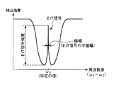
図1は、本発明の第1実施形態に係る原子発振器(量子干渉装置)を示す概略図である。また、図2は、アルカリ金属のエネルギー状態を説明するための図、図3は、光出射部から出射される2つの光の周波数差と、光検出部で検出される光の強度との関係を示すグラフである。
<First Embodiment>
FIG. 1 is a schematic diagram showing an atomic oscillator (quantum interference device) according to a first embodiment of the present invention. 2 is a diagram for explaining the energy state of the alkali metal, and FIG. 3 is a relationship between the frequency difference between the two lights emitted from the light emitting part and the intensity of the light detected by the light detecting part. It is a graph which shows.
図1に示す原子発振器1は、量子干渉効果を利用した原子発振器である。この原子発振器1は、図1に示すように、ガスセル2(原子セル)と、光出射部3と、光学部品41、42、43、44と、光検出部5と、ヒーター6と、温度センサー7と、磁場発生部8と、制御部10とを備える。
An
まず、原子発振器1の原理を簡単に説明する。
図1に示すように、原子発振器1では、光出射部3がガスセル2に向けて励起光LLを出射し、ガスセル2を透過した励起光LLを光検出部5が検出する。
First, the principle of the
As shown in FIG. 1, in the
ガスセル2内には、ガス状のアルカリ金属(金属原子)が封入されており、アルカリ金属は、図2に示すように、3準位系のエネルギー準位を有し、エネルギー準位の異なる2つの基底状態(基底状態1、2)と、励起状態との3つの状態をとり得る。ここで、基底状態1は、基底状態2よりも低いエネルギー状態である。
The
光出射部3から出射された励起光LLは、周波数の異なる2種の共鳴光1、2を含んでおり、この2種の共鳴光1、2を前述したようなガス状のアルカリ金属に照射したとき、共鳴光1の周波数ω1と共鳴光2の周波数ω2との差(ω1−ω2)に応じて、共鳴光1、2のアルカリ金属における光吸収率(光透過率)が変化する。
The excitation light LL emitted from the
そして、共鳴光1の周波数ω1と共鳴光2の周波数ω2との差(ω1−ω2)が基底状態1と基底状態2とのエネルギー差に相当する周波数に一致したとき、基底状態1、2から励起状態への励起がそれぞれ停止する。このとき、共鳴光1、2は、いずれも、アルカリ金属に吸収されずに透過する。このような現象をCPT現象または電磁誘起透明化現象(EIT:Electromagnetically Induced Transparency)と呼ぶ。
When the difference (ω1−ω2) between the frequency ω1 of the
例えば、光出射部3が共鳴光1の周波数ω1を固定し、共鳴光2の周波数ω2を変化させていくと、共鳴光1の周波数ω1と共鳴光2の周波数ω2との差(ω1−ω2)が基底状態1と基底状態2とのエネルギー差に相当する周波数ω0に一致したとき、光検出部5の検出強度は、図3に示すように、急峻に上昇する。このような急峻な信号をEIT信号として検出する。このEIT信号は、アルカリ金属の種類によって決まった固有値をもっている。したがって、このようなEIT信号を用いることにより、発振器を構成することができる。
For example, when the
以下、原子発振器1の各部を順次詳細に説明する。
[ガスセル]
ガスセル2内には、ガス状のルビジウム、セシウム、ナトリウム等のアルカリ金属が封入されている。また、ガスセル2内には、必要に応じて、アルゴン、ネオン等の希ガス、窒素等の不活性ガスが緩衝ガスとしてアルカリ金属ガスとともに封入されていてもよい。
Hereinafter, each part of the
[Gas cell]
The
後に詳述するが、ガスセル2は、貫通孔を有する胴部と、この胴部の貫通孔の開口を塞ぐ1対の窓部とを有し、これにより、気体状のアルカリ金属と、余剰分である液体状または固体状のアルカリ金属とが封入される内部空間が形成さている。すなわち、貫通孔の内面が、内部空間に接触している。
As will be described in detail later, the
[光出射部]
光出射部3(光源)は、ガスセル2中のアルカリ金属原子を励起する励起光LLを出射する機能を有する。
[Light emitting part]
The light emitting unit 3 (light source) has a function of emitting excitation light LL that excites alkali metal atoms in the
より具体的には、光出射部3は、励起光LLとして、前述したような周波数の異なる2種の光(共鳴光1および共鳴光2)を出射するものである。共鳴光1は、ガスセル2内のアルカリ金属を前述した基底状態1から励起状態へ励起(共鳴)し得るものである。一方、共鳴光2は、ガスセル2内のアルカリ金属を前述した基底状態2から励起状態へ励起(共鳴)し得るものである。
More specifically, the
この光出射部3としては、前述したような励起光を出射し得るものであれば、特に限定されないが、例えば、垂直共振器面発光レーザー(VCSEL)等の半導体レーザー等を用いることができる。
The
なお、光出射部3は、図示しない温度調節素子(発熱抵抗体、ペルチェ素子等)により、所定温度に温度調節される。
The
[光学部品]
複数の光学部品41、42、43、44は、それぞれ、前述した光出射部3とガスセル2との間における励起光LLの光路上に設けられている。ここで、光出射部3側からガスセル2側へ、光学部品41、光学部品42、光学部品43、光学部品44の順に配置されている。
[Optical parts]
The plurality of
光学部品41は、レンズである。これにより、励起光LLを無駄なくガスセル2へ照射することができる。
The
また、光学部品41は、励起光LLを平行光とする機能を有する。これにより、励起光LLがガスセル2の内壁で反射するのを簡単かつ確実に防止することができる。そのため、ガスセル2内での励起光の共鳴を好適に生じさせ、その結果、原子発振器1の発振特性を高めることができる。
The
光学部品42は、偏光板である。これにより、光出射部3からの励起光LLの偏光を所定方向に調整することができる。
The
光学部品43は、減光フィルター(NDフィルター)である。これにより、ガスセル2に入射する励起光LLの強度を調整(減少)させることができる。そのため、光出射部3の出力が大きい場合でも、ガスセル2に入射する励起光を所望の光量とすることができる。本実施形態では、前述した光学部品42を通過した所定方向の偏光を有する励起光LLの強度を光学部品43により調整する。
The
光学部品44は、λ/4波長板である。これにより、光出射部3からの励起光LLを直線偏光から円偏光(右円偏光または左円偏光)に変換することができる。
The
後述するように磁場発生部8の磁場によりガスセル2内のアルカリ金属原子がゼーマン分裂した状態において、仮に直線偏光の励起光をアルカリ金属原子に照射すると、励起光とアルカリ金属原子との相互作用により、アルカリ金属原子がゼーマン分裂した複数の準位に均等に分散して存在することとなる。その結果、所望のエネルギー準位のアルカリ金属原子の数が他のエネルギー準位のアルカリ金属原子の数に対して相対的に少なくなるため、所望のEIT現象を発現する原子数が減少し、所望のEIT信号の強度が小さくなり、その結果、原子発振器1の発振特性の低下をもたらす。
As will be described later, in the state where the alkali metal atoms in the
これに対し、後述するように磁場発生部8の磁場によりガスセル2内のアルカリ金属原子がゼーマン分裂した状態において、円偏光の励起光をアルカリ金属原子に照射すると、励起光とアルカリ金属原子との相互作用により、アルカリ金属原子がゼーマン分裂した複数の準位のうち、所望のエネルギー準位のアルカリ金属原子の数を他のエネルギー準位のアルカリ金属原子の数に対して相対的に多くすることができる。そのため、所望のEIT現象を発現する原子数が増大し、所望のEIT信号の強度が大きくなり、その結果、原子発振器1の発振特性を向上させることができる。
On the other hand, when the alkali metal atom is irradiated with circularly polarized excitation light in a state where the alkali metal atom in the
[光検出部]
光検出部5は、ガスセル2内を透過した励起光LL(共鳴光1、2)の強度を検出する機能を有する。
[Photodetection section]
The
この光検出部5としては、上述したような励起光を検出し得るものであれば、特に限定されないが、例えば、太陽電池、フォトダイオード等の光検出器(受光素子)を用いることができる。
The
[ヒーター]
ヒーター6(加熱部)は、前述したガスセル2(より具体的にはガスセル2中のアルカリ金属)を加熱する機能を有する。これにより、ガスセル2中のアルカリ金属を適切な濃度のガス状に維持することができる。
[heater]
The heater 6 (heating unit) has a function of heating the above-described gas cell 2 (more specifically, an alkali metal in the gas cell 2). Thereby, the alkali metal in the
このヒーター6は、例えば、通電により発熱する発熱抵抗体を含んで構成されている。この発熱抵抗体は、ガスセル2に対して接触して設けられていてもよいし、ガスセル2に対して非接触で設けられていてもよい。
The
例えば、発熱抵抗体をガスセル2に対して接触して設ける場合、ガスセル2の1対の窓部にそれぞれ発熱抵抗体を設ける。これにより、ガスセル2の窓部にアルカリ金属原子が結露するのを防止することができる。その結果、原子発振器1の特性(発振特性)を長期にわたり優れたものとすることができる。このような発熱抵抗体は、励起光に対する透過性を有する材料、具体的には、例えば、ITO(Indium Tin Oxide)、IZO(Indium Zinc Oxide)、In3O3、SnO2、Sb含有SnO2、Al含有ZnO等の酸化物等の透明電極材料で構成される。また、発熱抵抗体は、例えば、プラズマCVD、熱CVDのような化学蒸着法(CVD)、真空蒸着等の乾式メッキ法、ゾル・ゲル法等を用いて形成することができる。
For example, when the heating resistor is provided in contact with the
また、発熱抵抗体をガスセル2に対して非接触で設ける場合、熱伝導性に優れる金属等、セラミックス等の部材を介して発熱抵抗体からガスセル2へ伝熱すればよい。
Further, when the heating resistor is provided in a non-contact manner with respect to the
なお、ヒーター6は、ガスセル2を加熱することができるものであれば、前述した形態に限定されず、各種ヒーターを用いることができる。また、ヒーター6に代えて、または、ヒーター6と併用して、ペルチェ素子を用いて、ガスセル2を加熱してもよい。
The
[温度センサー]
温度センサー7は、ヒーター6またはガスセル2の温度を検出するものである。そして、この温度センサー7の検出結果に基づいて、前述したヒーター6の発熱量が制御される。これにより、ガスセル2内のアルカリ金属原子を所望の温度に維持することができる。
[Temperature sensor]
The temperature sensor 7 detects the temperature of the
なお、温度センサー7の設置位置は、特に限定されず、例えば、ヒーター6上であってもよいし、ガスセル2の外表面上であってもよい。
The installation position of the temperature sensor 7 is not particularly limited, and may be on the
温度センサー7としては、それぞれ、特に限定されず、サーミスタ、熱電対等の公知の各種温度センサーを用いることができる。 The temperature sensor 7 is not particularly limited, and various known temperature sensors such as a thermistor and a thermocouple can be used.
[磁場発生部]
磁場発生部8は、ガスセル2内のアルカリ金属の縮退した複数のエネルギー準位をゼーマン分裂させる磁場を発生させる機能を有する。これにより、ゼーマン分裂により、アルカリ金属の縮退している異なるエネルギー準位間のギャップを拡げて、分解能を向上させることができる。その結果、原子発振器1の発振周波数の精度を高めることができる。
[Magnetic field generator]
The magnetic
この磁場発生部8は、例えば、ガスセル2を挟むように配置されたヘルムホルツコイル、または、ガスセル2を覆うように配置されたソレノイドコイルで構成されている。これにより、ガスセル2内に一方向の均一な磁場を生じさせることができる。
The
また、磁場発生部8が発生する磁場は、定磁場(直流磁場)であるが、交流磁場が重畳されていてもよい。
The magnetic field generated by the
[制御部]
制御部10は、光出射部3、ヒーター6および磁場発生部8をそれぞれ制御する機能を有する。
[Control unit]
The
この制御部10は、光出射部3の共鳴光1、2の周波数を制御する励起光制御部12と、ガスセル2中のアルカリ金属の温度を制御する温度制御部11と、磁場発生部8からの磁場を制御する磁場制御部13とを有する。
The
励起光制御部12は、前述した光検出部5の検出結果に基づいて、光出射部3から出射される共鳴光1、2の周波数を制御する。より具体的には、励起光制御部12は、前述した周波数差(ω1−ω2)が前述したアルカリ金属固有の周波数ω0となるように、光出射部3から出射される共鳴光1、2の周波数を制御する。
The excitation
ここで、励起光制御部12は、図示しないが、電圧制御型水晶発振器(発振回路)を備えており、その電圧制御型水晶発振器の発振周波数を光検出部5の検知結果に基づいて同期・調整しながら、その電圧制御型水晶発振器の出力信号を原子発振器1の出力信号として出力する。
Here, although not shown, the excitation
例えば、励起光制御部12は、図示しないが、この電圧制御型水晶発振器からの出力信号を周波数逓倍する逓倍器を備えており、この逓倍器により逓倍された信号(高周波信号)を直流バイアス電流に重畳して駆動信号として光出射部3に入力する。これにより、光検出部5でEIT信号が検出されるように電圧制御型水晶発振器を制御することで、電圧制御型水晶発振器から所望の周波数の信号が出力されることとなる。この逓倍器の逓倍率は、例えば、原子発振器1からの出力信号の所望の周波数をfとしたとき、ω0/(2×f)である。これにより、電圧制御型水晶発振器の発振周波数がfであるとき、逓倍器からの信号を用いて、光出射部3に含まれる半導体レーザー等の発光素子を変調して、周波数差(ω1−ω2)がω0となる2つの光を出射させることができる。
For example, although not shown, the pumping
また、温度制御部11は、温度センサー7の検出結果に基づいて、ヒーター6への通電を制御する。これにより、ガスセル2を所望の温度範囲内に維持することができる。例えば、ガスセル2は、ヒーター6により、例えば、70℃程度に温度調節される。
Further, the temperature control unit 11 controls energization to the
また、磁場制御部13は、磁場発生部8が発生する磁場が一定となるように、磁場発生部8への通電を制御する。
The magnetic
このような制御部10は、例えば、基板上に実装されたICチップに設けられている。
以上、原子発振器1の構成を簡単に説明した。
Such a
The configuration of the
(ガスセルの詳細な説明)
図4は、図1に示す原子発振器が備える原子セルの斜視図、図5(a)は、図4に示す原子セルの横断面図、図5(b)は、図4に示す原子セルの縦断面図である。
(Detailed description of gas cell)
4 is a perspective view of the atomic cell included in the atomic oscillator shown in FIG. 1, FIG. 5A is a cross-sectional view of the atomic cell shown in FIG. 4, and FIG. 5B is a cross-sectional view of the atomic cell shown in FIG. It is a longitudinal cross-sectional view.
なお、図4では、説明の便宜上、互いに直交する3つの軸として、X軸、Y軸およびZ軸を図示しており、その図示された各矢印の先端側を「+(プラス)」、基端側を「−(マイナス)」という。また、以下では、説明の便宜上、X軸に平行な方向を「X軸方向」、Y軸に平行な方向を「Y軸方向」、Z軸に平行な方向を「Z軸方向」という。また、+Z軸方向側を「上」、−Z軸方向側を「下」ともいう。 In FIG. 4, for convenience of explanation, the X axis, the Y axis, and the Z axis are illustrated as three axes orthogonal to each other, and “+ (plus)” is used as the base side of each illustrated arrow. The end side is called "-(minus)". Hereinafter, for convenience of explanation, a direction parallel to the X axis is referred to as an “X axis direction”, a direction parallel to the Y axis is referred to as a “Y axis direction”, and a direction parallel to the Z axis is referred to as a “Z axis direction”. The + Z-axis direction side is also referred to as “upper”, and the −Z-axis direction side is also referred to as “lower”.
図4および図5に示すように、ガスセル2は、胴体部21と、胴体部21を挟んで設けられた1対の窓部22、23とを有している。
As shown in FIGS. 4 and 5, the
胴体部21には、Z軸方向に貫通している貫通孔211が形成されている。この貫通孔211は、円柱状の貫通孔211a、211bと、貫通孔211a、211b間を連通させるスリット状の貫通孔211cとで構成されている。ここで、貫通孔211bの内壁面には、液体状のアルカリ金属Mを保持させる保持部24(金属接続部)が設けられている。なお、保持部24については、後に詳述する。
A through
胴体部21の構成材料としては、特に限定されず、ガラス材料、水晶、金属材料、樹脂材料、シリコン材料等が挙げられるが、中でも、ガラス材料、水晶、シリコン材料のいずれかを用いることが好ましく、シリコン材料を用いることがより好ましい。これにより、幅や高さが10mm以下となるような小さいガスセル2を形成する場合であっても、エッチング等の微細加工技術を用いて、高精度な胴体部21を容易に形成することができる。
The constituent material of the
そして、胴体部21の−Z軸方向側の端面(下端面)には、窓部22が接合され、一方、胴体部21の+Z軸方向側の端面(上端面)には、窓部23が接合されている。これにより、貫通孔211の両端開口が封鎖され、貫通孔211aによる空間S1と、貫通孔211bによる空間S2と、貫通孔211cによる空間S3とを有する内部空間Sが形成されている。この内部空間Sには、アルカリ金属が収納されている。ここで、胴体部21および1対の窓部22、23は、アルカリ金属が封入されている内部空間Sを構成している「壁部」であるといえる。
The
胴体部21と窓部22、23との接合方法としては、これらの構成材料に応じて決められるものであり、気密的に接合できるものであれば、特に限定されないが、例えば、接着剤による接合方法、直接接合法、陽極接合法等を用いることができる。
The joining method of the
空間S1は、主に、気体状のアルカリ金属が収納されており、この空間S1内に収納されている気体状のアルカリ金属は、励起光LLによって励起される。すなわち、空間S1は、励起光LLが通過する「光通過空間」を構成する。本実施形態では、空間S1の横断面は、円形をなしており、一方、光通過空間の横断面は、空間S1の横断面と相似形状をなし、かつ、空間S1の横断面よりも若干小さく設定されている。なお、空間S1の横断面形状は、円形に限定されず、例えば、四角形、五角形等の多角形、楕円形等であってもよい。 The space S1 mainly contains gaseous alkali metal, and the gaseous alkali metal accommodated in the space S1 is excited by the excitation light LL. That is, the space S1 constitutes a “light passage space” through which the excitation light LL passes. In the present embodiment, the cross section of the space S1 has a circular shape, while the cross section of the light passage space has a similar shape to the cross section of the space S1 and is slightly smaller than the cross section of the space S1. Is set. The cross-sectional shape of the space S1 is not limited to a circle, and may be, for example, a polygon such as a quadrangle or a pentagon, or an ellipse.
空間S2は、液体状または固体状のアルカリ金属Mが収納されている金属溜り部である。この空間S2は、空間S3を介して空間S1に連通している。したがって、アルカリ金属Mは、空間S1内の気体状のアルカリ金属が不足したとき、その蒸気圧を保とうとするために気体状となって、励起光LLの励起に供される。この空間S2の幅(XY平面に沿った断面の長さ)は、空間S1の幅よりも狭い。これにより、ガスセル2の小型化を図ることができる。
The space S2 is a metal reservoir in which a liquid or solid alkali metal M is stored. This space S2 communicates with the space S1 via the space S3. Accordingly, the alkali metal M becomes gaseous in order to maintain its vapor pressure when the gaseous alkali metal in the space S1 is insufficient, and is used for excitation of the excitation light LL. The width of the space S2 (the length of the cross section along the XY plane) is narrower than the width of the space S1. Thereby, size reduction of the
このような空間S1、S2、S3は、前述したように、胴体部21に形成されている貫通孔211の両端開口が1対の窓部22、23により封鎖されることにより形成されている。これにより、空間S1、S2、S3を有する小型なガスセル2を高精度かつ簡単に形成することができる。具体的には、例えば、シリコン基板やガラス基板等の基板をエッチング等の微細加工技術を用いて加工することにより、小型でかつ高精度な胴体部21を容易かつ効率的に作成することができる。そのため、小型なガスセル2を高精度かつ簡単に形成することができる。特に、CPTを利用した方式の原子発振器は、二重共鳴現象を利用した方式の原子発振器に比し、小型化に向いており、近年、様々な機器への組み込みが期待され、さらなる小型化の要請も強いことから、小型なガスセル2を高精度かつ簡単に形成することができるという効果は、CPTを利用した方式の原子発振器1において重要となる。
As described above, the spaces S1, S2, and S3 are formed by sealing both end openings of the through
このような空間S2の具体的な幅は、余剰分のアルカリ金属Mの体積やガスセル2全体の体積等に応じて決められるものであり、特に限定されないが、0.1mm以上2mm以下であることが好ましく、0.1mm以上1mm以下であることがより好ましい。
The specific width of the space S2 is determined according to the volume of the excess alkali metal M, the volume of the
また、本実施形態では、図5(a)に示すように、Z軸方向から見たとき、空間S2が円形をなしている。なお、空間S2の横断面形状は、円形に限定されず、例えば、四角形、五角形等の多角形、楕円形等であってもよい。 In the present embodiment, as shown in FIG. 5A, the space S2 has a circular shape when viewed from the Z-axis direction. The cross-sectional shape of the space S2 is not limited to a circle, and may be a polygon such as a quadrangle or a pentagon, an ellipse, or the like.
また、空間S1と空間S2とを連通させている空間S3は、Z軸方向から見たとき、直線的に延びた形状をなしている。なお、空間S3の横断面形状は、屈曲または湾曲した部分を有していてもよい。 Further, the space S3 that connects the space S1 and the space S2 has a linearly extending shape when viewed from the Z-axis direction. Note that the cross-sectional shape of the space S3 may have a bent or curved portion.
このような空間S3の幅は、空間S2よりも狭い。これにより、アルカリ金属Mを収納する空間S2の大きさを確保しつつ、空間S1内の気体状のアルカリ金属に対するアルカリ金属Mの影響を低減することができる。なお、空間S3の幅は、空間S2の幅と同じであってもよい。また、空間S3は、空間S1と空間S2とを連通させることができればよく、胴体部21のZ軸方向の全域にわたらずに一部に形成されていてもよい。この場合、胴体部21のZ軸方向での一端側の面に溝を形成すればよい。
The width of the space S3 is narrower than the space S2. Thereby, the influence of the alkali metal M with respect to the gaseous alkali metal in space S1 can be reduced, ensuring the magnitude | size of the space S2 in which the alkali metal M is accommodated. Note that the width of the space S3 may be the same as the width of the space S2. The space S3 only needs to be able to communicate the space S1 and the space S2, and may be formed in a part of the
このような胴体部21に接合されている各窓部22、23は、前述した光出射部3からの励起光に対する透過性を有している。そして、一方の窓部22は、ガスセル2の空間S1内へ励起光LLが入射する入射側窓部であり、他方の窓部23は、ガスセル2の空間S1内から励起光LLが出射する出射側窓部である。
また、窓部22、23は、それぞれ、板状をなしている。
Each
Each of the
窓部22、23の構成材料としては、前述したような励起光に対する透過性を有していれば、特に限定されないが、例えば、ガラス材料、水晶等が挙げられる。窓部22、23をガラス材料で構成した場合、シリコン材料で構成された胴体部21と窓部22、23とを陽極接合法により簡単に気密的に接合することができる。なお、窓部22、23の厚さや励起光の波長や強度によっては、窓部22、23をシリコンで構成することもできる。
Although it will not specifically limit as a constituent material of the
以上説明したように構成されたガスセル2は、前述したように、アルカリ金属の一部が内部空間Sで液体状のアルカリ金属Mとして存在している。このように液体状のアルカリ金属Mが余剰分として内部空間Sに存在している場合、液体状のアルカリ金属Mが移動したり振れたりすると、特性が低下する問題が生じる。
As described above, in the
そこで、前述したように、貫通孔211bの内壁面に、液体状のアルカリ金属Mを保持する保持部24(金属接続部)が設けられている。以下、保持部24について詳述する。
Therefore, as described above, the holding portion 24 (metal connection portion) that holds the liquid alkali metal M is provided on the inner wall surface of the through
図6(a)は、図5に示す金属接続部(金属溜り部)における液体状の金属の状態を示す図、図6(b)は、原子セルの内壁面に対する液体状の金属の接触角と周波数変動との関係を示すグラフである。 6A is a diagram showing a state of liquid metal in the metal connection portion (metal reservoir portion) shown in FIG. 5, and FIG. 6B is a contact angle of the liquid metal with respect to the inner wall surface of the atomic cell. It is a graph which shows the relationship between frequency fluctuation.
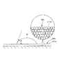
保持部24は、図6(a)に示すように、液体状のアルカリ金属Mの接触角θが90°よりも小さくなるように構成されている。これにより、液体状のアルカリ金属Mに対する保持部24の濡れ性が高いため、余剰の液体状のアルカリ金属Mを保持部24に濡れ拡がらせて安定的に保持させることができる。そのため、液体状のアルカリ金属Mが移動したり振れたりするのを低減すること(すなわち、ガスセル2内の液体状のアルカリ金属Mの挙動を安定化させること)ができ、その結果、余剰分のアルカリ金属Mによる特性の低下を抑制することができる。
As shown in FIG. 6A, the holding
本実施形態では、保持部24は、金属溜り部である空間S2に配置されているため、ガスセル2の特性の影響の少ない部位に、液体状のアルカリ金属Mを留まらせておくことができる。
In this embodiment, since the holding
この保持部24は、図6(a)に示すように、貫通孔211bの内壁面を粗面化処理することによって形成されている。すなわち、保持部24は、微細な複数の凹部または凸部で構成されている。本実施形態では、保持部24は、エッチングにより粗面化されている。これにより、比較的簡単な構成で、余剰の液体状のアルカリ金属Mを保持部24に濡れ拡がらせて安定的に保持させることができる。例えば、胴体部21および窓部22、23がシリコンまたはガラスで構成されている場合、フッ素プラズマを用いたドライエッチングにより、前述したような保持部24の凹部または凸部を形成することができる。
As shown in FIG. 6A, the holding
また、このような粗面化処理は、胴体部21と窓部22、23との接合面を除く面に行うことが好ましい。これにより、胴体部21と窓部22、23との気密的な接合を簡単かつ確実に行うことができる。
Such roughening treatment is preferably performed on the surface excluding the joint surface between the
また、このような粗面化処理は、窓部22、23の励起光LLが通過する面を除いて行うことが好ましい。このように、1対の窓部22、23が、液体状のアルカリ金属Mの接触角が保持部24よりも大きい部分を有することにより、窓部22、23に液体状のアルカリ金属が付着するのを低減することができる。特に、窓部22、23の励起光LLが通過する面に液体状のアルカリ金属が付着することによる特性の低下を防止できる。
Moreover, it is preferable to perform such a roughening process except the surface through which the excitation light LL of the
また、保持部24に対する液体状のアルカリ金属Mの接触角θは、0°よりも大きく、かつ、90°よりも小さい範囲内にあれば、図6(b)に示すように、1日当たりの周波数変動量Δfを効果的に小さくすることができるが、保持部24に対する液体状のアルカリ金属Mの濡れ性をより高める観点から、70°よりも小さいことが好ましく、60°よりも小さいことがより好ましい。
Further, when the contact angle θ of the liquid alkali metal M with respect to the holding
また、前述したように窓部22、23の励起光LLが通過する面に液体状のアルカリ金属が付着することによる特性の低下を防止する観点から、窓部22、23の励起光LLが通過する面(内壁面)に対する液体状のアルカリ金属の接触角は、90°以上であることが好ましく、100°以上であることがより好ましい。
In addition, as described above, the excitation light LL of the
また、保持部24の中心線平均粗さRa(以下、表面粗さRa)は、10nm以上980nm以下の範囲内にあることが好ましく、100nm以上800nm以下の範囲内にあることがより好ましく、300nm以上700nm以下の範囲内にあることがさらに好ましい。これにより、比較的簡単な構成で、余剰の液体状のアルカリ金属Mを保持部24に濡れ拡がらせて安定的に保持させることができる。なお、このような表面粗さRaは、JIS B0601:2001に基づき、例えば、触針式の表面粗さ計、レーザー等を用いた非接触式表面粗さ計、および原子間力顕微鏡(AFM)などを用いて測定することができる。
The center line average roughness Ra (hereinafter referred to as surface roughness Ra) of the holding
また、胴体部21および窓部22、23は、それぞれ、シリコンまたはガラスで構成されていることが好ましい。これにより、ガスセル2に必要な基本的機能を確保しながら、エッチングや成膜により前述したような複数の凹部または凸部を有する保持部24を比較的簡単に形成することができる。
Moreover, it is preferable that the trunk | drum 21 and the
<第2実施形態>
次に、本発明の第2実施形態について説明する。
Second Embodiment
Next, a second embodiment of the present invention will be described.
図7(a)は、本発明の第2実施形態に係る原子セルの横断面図、図7(b)は、図7(a)に示す原子セルの縦断面図である。また、図8は、図7に示す金属接続部(金属溜り部)における液体状の金属の状態を示す図である。 FIG. 7A is a transverse sectional view of an atomic cell according to the second embodiment of the present invention, and FIG. 7B is a longitudinal sectional view of the atomic cell shown in FIG. 7A. Moreover, FIG. 8 is a figure which shows the state of the liquid metal in the metal connection part (metal reservoir part) shown in FIG.
本実施形態は、金属接続部の構成が異なる以外は、前述した第1実施形態と同様である。 The present embodiment is the same as the first embodiment described above except that the configuration of the metal connection portion is different.
なお、以下の説明では、第2実施形態に関し、前述した実施形態との相違点を中心に説明し、同様の事項に関してはその説明を省略する。また、図7および図8において、前述した実施形態と同様の構成については、同一符号を付している。 In the following description, the second embodiment will be described with a focus on differences from the above-described embodiment, and description of similar matters will be omitted. 7 and 8, the same reference numerals are given to the same configurations as those in the above-described embodiment.
図7に示すガスセル2A(原子セル)は、第1実施形態の胴体部21に代えて、胴体部21Aを備えている。
A
胴体部21Aには、Z軸方向に貫通している貫通孔211Aが形成されている。この貫通孔211Aは、円柱状の貫通孔211a、211dと、貫通孔211a、211d間を連通させるスリット状の貫通孔211cとで構成されている。
A through
貫通孔211dの内壁面には、液体状のアルカリ金属Mを保持させる保持部24Aが設けられている。この保持部24Aは、図8に示すように、多孔質膜で構成されている。このような多孔質膜を設けることによっても、前述した第1実施形態の保持部24の粗面化処理と同様の効果を奏することができる。また、比較的簡単な構成で、余剰の液体状のアルカリ金属を保持部24Aに濡れ拡がらせて安定的に保持させることができる。
A holding
このような多孔質膜で構成された保持部24Aは、例えば、多孔質ポリシリコン、多孔質シリカ等の無機多孔質で構成されている。また、このような保持部24Aの形成は、CVD等の気相成膜法を用いて行ってもよいし、有機物のバインダーを含む無機微粒子を塗布した後に焼成・焼結することによって行ってもよい。
The holding
以上説明したような第2実施形態によっても、余剰分のアルカリ金属Mによる特性の低下を抑制することができる。 Also according to the second embodiment as described above, it is possible to suppress deterioration of characteristics due to the excess alkali metal M.
<第3実施形態>
次に、本発明の第3実施形態について説明する。
<Third Embodiment>
Next, a third embodiment of the present invention will be described.
図9(a)は、本発明の第3実施形態に係る原子セルの横断面図、図9(b)は、図9(a)に示す原子セルの縦断面図である。 FIG. 9A is a transverse sectional view of an atomic cell according to the third embodiment of the present invention, and FIG. 9B is a longitudinal sectional view of the atomic cell shown in FIG. 9A.
本実施形態は、原子セルの内部空間の形状および金属接続部の構成が異なる以外は、前述した第1実施形態と同様である。また、本実施形態は、原子セルの内部空間の形状が異なる以外は、前述した第2実施形態と同様である。 This embodiment is the same as the first embodiment described above except that the shape of the internal space of the atomic cell and the configuration of the metal connection portion are different. Further, this embodiment is the same as the second embodiment described above except that the shape of the internal space of the atomic cell is different.
なお、以下の説明では、第3実施形態に関し、前述した実施形態との相違点を中心に説明し、同様の事項に関してはその説明を省略する。また、図9において、前述した実施形態と同様の構成については、同一符号を付している。 In the following description, the third embodiment will be described with a focus on differences from the above-described embodiment, and description of similar matters will be omitted. In FIG. 9, the same reference numerals are given to the same configurations as those in the above-described embodiment.
図9に示すガスセル2B(原子セル)は、第1実施形態の胴体部21に代えて、胴体部21Bを備えている。
A
胴体部21Bには、Z軸方向に貫通している貫通孔211Bが形成されている。この貫通孔211Bは、円柱状の貫通孔211aで構成されている。
A through
貫通孔211Bの内壁面には、液体状のアルカリ金属Mを保持させる保持部24Bが設けられている。これにより、比較的簡単な構成で、余剰の液体状のアルカリ金属を保持部24Aに濡れ拡がらせて安定的に保持させることができる。ここで、本実施形態では、保持部24Bが「金属溜り部」を構成しており、貫通孔211Bにより形成される光通過空間である空間Sは、金属溜り部を含んでいるといえる。
A holding
また、保持部24Bは、胴体部21Bと窓部22、23との接合面を除く面に配置されている。これにより、胴体部21Bと窓部22、23との気密的な接合を簡単かつ確実に行うことができる。
The holding
また、保持部24Bは、窓部22、23の内壁面にも設けられているが、窓部22、23の励起光LLが通過する面を除いて配置されている。これにより、窓部22、23の励起光LLが通過する面に液体状のアルカリ金属が付着することによる特性の低下を防止できる。
The holding
以上説明したような第3実施形態によっても、余剰分のアルカリ金属Mによる特性の低下を抑制することができる。 Also according to the third embodiment as described above, it is possible to suppress deterioration of characteristics due to the excess alkali metal M.
2.電子機器
以上説明したような原子発振器は、各種電子機器に組み込むことができる。このような電子機器は、優れた信頼性を有する。
2. Electronic equipment The atomic oscillator described above can be incorporated into various electronic equipment. Such an electronic device has excellent reliability.
以下、本発明の電子機器について説明する。
図10は、GPS衛星を利用した測位システムに本発明の原子発振器を用いた場合の概略構成を示す図である。
Hereinafter, the electronic apparatus of the present invention will be described.
FIG. 10 is a diagram showing a schematic configuration when the atomic oscillator of the present invention is used in a positioning system using a GPS satellite.
図10に示す測位システム100は、GPS衛星200と、基地局装置300と、GPS受信装置400とで構成されている。
The
GPS衛星200は、測位情報(GPS信号)を送信する。
基地局装置300は、例えば電子基準点(GPS連続観測局)に設置されたアンテナ301を介してGPS衛星200からの測位情報を高精度に受信する受信装置302と、この受信装置302で受信した測位情報をアンテナ303を介して送信する送信装置304とを備える。
The
The
ここで、受信装置302は、その基準周波数発振源として前述した本発明の原子発振器1を備える電子装置である。このような受信装置302は、優れた信頼性を有する。また、受信装置302で受信された測位情報は、リアルタイムで送信装置304により送信される。
Here, the receiving
GPS受信装置400は、GPS衛星200からの測位情報をアンテナ401を介して受信する衛星受信部402と、基地局装置300からの測位情報をアンテナ403を介して受信する基地局受信部404とを備える。
The
3.移動体
図11は、移動体の一例を示す図である。
3. Mobile 11 is a diagram showing an example of a moving body.
この図において、移動体1500は、車体1501と、4つの車輪1502とを有しており、車体1501に設けられた図示しない動力源(エンジン)によって車輪1502を回転させるように構成されている。このような移動体1500には、原子発振器1が内蔵されている。
このような移動体によれば、優れた信頼性を発揮することができる。
In this figure, a moving
According to such a moving body, excellent reliability can be exhibited.
なお、本発明の電子機器は、前述したものに限定されず、例えば、携帯電話機、ディジタルスチルカメラ、インクジェット式吐出装置(例えばインクジェットプリンター)、パーソナルコンピューター(モバイル型パーソナルコンピューター、ラップトップ型パーソナルコンピューター)、テレビ、ビデオカメラ、ビデオテープレコーダー、カーナビゲーション装置、ページャー、電子手帳(通信機能付も含む)、電子辞書、電卓、電子ゲーム機器、ワードプロセッサー、ワークステーション、テレビ電話、防犯用テレビモニター、電子双眼鏡、POS端末、医療機器(例えば電子体温計、血圧計、血糖計、心電図計測装置、超音波診断装置、電子内視鏡)、魚群探知機、各種測定機器、計器類(例えば、車両、航空機、船舶の計器類)、フライトシミュレーター、地上デジタル放送、携帯電話基地局等に適用することができる。 Note that the electronic apparatus of the present invention is not limited to the above-described ones. For example, a mobile phone, a digital still camera, an ink jet discharge device (for example, an ink jet printer), a personal computer (a mobile personal computer, a laptop personal computer). , TV, camcorder, video tape recorder, car navigation device, pager, electronic notebook (including communication function), electronic dictionary, calculator, electronic game device, word processor, workstation, video phone, security TV monitor, electronic binoculars POS terminal, medical equipment (eg electronic thermometer, blood pressure monitor, blood glucose meter, electrocardiogram measuring device, ultrasonic diagnostic device, electronic endoscope), fish detector, various measuring equipment, instruments (eg, vehicle, aircraft, ship) Instrumentation) Ito simulator, terrestrial digital broadcasting, can be applied to a mobile phone base station or the like.
以上、本発明の原子セル、量子干渉装置、原子発振器および電子機器について、図示の実施形態に基づいて説明したが、本発明は、これらに限定されるものではない。 Above, atomic cell of the present invention, quantum interference device, the atomic oscillator and electronic equipment has been described with reference to the illustrated embodiments, the present invention is not limited thereto.
また、本発明の各部の構成は、前述した実施形態の同様の機能を発揮する任意の構成のものに置換することができ、また、任意の構成を付加することもできる。 Moreover, the structure of each part of this invention can be substituted by the thing of the arbitrary structures which exhibit the same function of embodiment mentioned above, and arbitrary structures can also be added.
また、本発明は、前述した各実施形態の任意の構成同士を組み合わせるようにしてもよい。 Moreover, you may make it this invention combine arbitrary structures of each embodiment mentioned above.
また、前述した実施形態では、波長の異なる2種類の光による量子干渉効果を利用してセシウム等を共鳴遷移させる量子干渉装置に本発明の原子セルを用いた場合を例として説明したが、本発明の原子セルは、これに限定されず、光およびマイクロ波による二重共鳴現象を利用してルビジウム等を共鳴遷移させる二重共鳴装置にも用いることができる。 In the above-described embodiment, the case where the atomic cell of the present invention is used in a quantum interference device that resonantly transitions cesium or the like using the quantum interference effect of two types of light having different wavelengths has been described as an example. The atomic cell of the invention is not limited to this, and can also be used for a double resonance apparatus that makes a resonance transition of rubidium or the like by utilizing a double resonance phenomenon caused by light and microwaves.
1‥‥原子発振器
2‥‥ガスセル
2A‥‥ガスセル
2B‥‥ガスセル
3‥‥光出射部
5‥‥光検出部
6‥‥ヒーター
7‥‥温度センサー
8‥‥磁場発生部
10‥‥制御部
11‥‥温度制御部
12‥‥励起光制御部
13‥‥磁場制御部
21‥‥胴体部
21A‥‥胴体部
21B‥‥胴体部
22‥‥窓部
23‥‥窓部
24‥‥保持部(金属接続部)
24A‥‥保持部(金属接続部)
24B‥‥保持部(金属接続部)
41‥‥光学部品
42‥‥光学部品
43‥‥光学部品
44‥‥光学部品
100‥‥測位システム
200‥‥GPS衛星
211‥‥貫通孔
211A‥‥貫通孔
211B‥‥貫通孔
211a‥‥貫通孔
211b‥‥貫通孔
211c‥‥貫通孔
211d‥‥貫通孔
300‥‥基地局装置
301‥‥アンテナ
302‥‥受信装置
303‥‥アンテナ
304‥‥送信装置
400‥‥GPS受信装置
401‥‥アンテナ
402‥‥衛星受信部
403‥‥アンテナ
404‥‥基地局受信部
1500‥‥移動体
1501‥‥車体
1502‥‥車輪
LL‥‥励起光
M‥‥アルカリ金属
S‥‥内部空間
S1‥‥空間(光通過部)
S2‥‥空間(金属溜り部)
S3‥‥空間
Δf‥‥周波数変動量
θ‥‥接触角
DESCRIPTION OF
24A ... Holding part (metal connection part)
24B ... Holding part (metal connection part)
41 ...
S2 ... space (metal reservoir)
S3 Space Δf Frequency variation θ Contact angle
Claims (10)
前記金属が封入されている内部空間を構成している壁部と、
を備え、
前記壁部の内壁面は、液体状の前記金属を保持する金属接続部を有し、
前記金属接続部は、微細な複数の凹部または凸部が形成された粗面化状態となっており、前記粗面化状態により、液体状の前記金属との接触角が90°よりも小さくなっており、
前記金属接続部の表面粗さRaは、10nm以上980nm以下の範囲内にあることを特徴とする原子セル。 Metal,
A wall constituting an internal space in which the metal is enclosed;
With
An inner wall surface of the wall, have a metal connection portion for holding a liquid the metal,
The metal connecting portion has a roughened state having a plurality of recesses or protrusions fine is formed, wherein a roughened state, the contact angle with a liquid form of said metal is rather smaller than 90 ° And
The atomic cell having a surface roughness Ra of the metal connection portion in a range of 10 nm to 980 nm .
前記金属が封入されている内部空間を構成している壁部と、
を備え、
前記壁部の内壁面は、液体状の前記金属を保持する金属接続部を有し、
前記金属接続部は、微細な複数の凹部または凸部が形成された粗面化状態となっており、前記粗面化状態により、液体状の前記金属との接触角が90°よりも小さくなっており、
前記金属接続部は、多孔質膜を含むことを特徴とする原子セル。 Metal,
A wall constituting an internal space in which the metal is enclosed;
With
An inner wall surface of the wall, have a metal connection portion for holding a liquid the metal,
The metal connecting portion has a roughened state having a plurality of recesses or protrusions fine is formed, wherein a roughened state, the contact angle with a liquid form of said metal is rather smaller than 90 ° And
The atomic cell , wherein the metal connection part includes a porous film .
前記金属が封入されている内部空間を構成している壁部と、
を備え、
前記壁部の内壁面は、液体状の前記金属を保持する金属接続部を有し、
前記金属接続部は、微細な複数の凹部または凸部が形成された粗面化状態となっており、前記粗面化状態により、液体状の前記金属との接触角が90°よりも小さくなっており、
前記金属の一部が前記内部空間で液体状となっており、
前記内部空間は、前記液体状の金属が配置されている金属溜り部を有し、
前記金属接続部は、前記金属溜り部を構成する内壁面に配置されており、
前記金属溜り部の内壁面は、エッチングにより粗面化されていることを特徴とする原子セル。 Metal,
A wall constituting an internal space in which the metal is enclosed;
With
An inner wall surface of the wall, have a metal connection portion for holding a liquid the metal,
The metal connecting portion has a roughened state having a plurality of recesses or protrusions fine is formed, wherein a roughened state, the contact angle with a liquid form of said metal is rather smaller than 90 ° And
A portion of the metal is liquid in the internal space;
The internal space has a metal reservoir in which the liquid metal is disposed,
The metal connection part is disposed on an inner wall surface constituting the metal reservoir part,
An atomic cell in which an inner wall surface of the metal reservoir is roughened by etching .
前記金属が封入されている内部空間を構成している壁部と、
を備え、
前記壁部の内壁面は、液体状の前記金属を保持する金属接続部を有し、
前記金属接続部は、微細な複数の凹部または凸部が形成された粗面化状態となっており、前記粗面化状態により、液体状の前記金属との接触角が90°よりも小さくなっており、
前記壁部は、1対の窓部を有しており、
前記各窓部の前記内部空間側の面は、液体状の前記金属の接触角が前記金属接続部よりも大きい部分を有することを特徴とする原子セル。 Metal,
A wall constituting an internal space in which the metal is enclosed;
With
An inner wall surface of the wall, have a metal connection portion for holding a liquid the metal,
The metal connecting portion has a roughened state having a plurality of recesses or protrusions fine is formed, wherein a roughened state, the contact angle with a liquid form of said metal is rather smaller than 90 ° And
The wall has a pair of windows,
The atomic cell , wherein the surface of each window portion on the inner space side has a portion in which a contact angle of the liquid metal is larger than that of the metal connection portion .
Priority Applications (3)
| Application Number | Priority Date | Filing Date | Title |
|---|---|---|---|
| JP2014059250A JP6435617B2 (en) | 2014-03-20 | 2014-03-20 | Atomic cell, quantum interference device, atomic oscillator and electronic equipment |
| US14/662,584 US9755654B2 (en) | 2014-03-20 | 2015-03-19 | Atomic cell, quantum interference device, atomic oscillator, electronic device and moving object |
| CN201510121871.3A CN104935339A (en) | 2014-03-20 | 2015-03-19 | Atomic cell, quantum interference device, atomic oscillator, electronic device and moving object |
Applications Claiming Priority (1)
| Application Number | Priority Date | Filing Date | Title |
|---|---|---|---|
| JP2014059250A JP6435617B2 (en) | 2014-03-20 | 2014-03-20 | Atomic cell, quantum interference device, atomic oscillator and electronic equipment |
Publications (3)
| Publication Number | Publication Date |
|---|---|
| JP2015185958A JP2015185958A (en) | 2015-10-22 |
| JP2015185958A5 JP2015185958A5 (en) | 2017-04-20 |
| JP6435617B2 true JP6435617B2 (en) | 2018-12-12 |
Family
ID=54122335
Family Applications (1)
| Application Number | Title | Priority Date | Filing Date |
|---|---|---|---|
| JP2014059250A Expired - Fee Related JP6435617B2 (en) | 2014-03-20 | 2014-03-20 | Atomic cell, quantum interference device, atomic oscillator and electronic equipment |
Country Status (3)
| Country | Link |
|---|---|
| US (1) | US9755654B2 (en) |
| JP (1) | JP6435617B2 (en) |
| CN (1) | CN104935339A (en) |
Families Citing this family (8)
| Publication number | Priority date | Publication date | Assignee | Title |
|---|---|---|---|---|
| US10145909B2 (en) * | 2014-11-17 | 2018-12-04 | Seiko Epson Corporation | Magnetism measuring device, gas cell, manufacturing method of magnetism measuring device, and manufacturing method of gas cell |
| US10295488B2 (en) * | 2016-01-11 | 2019-05-21 | Texas Instruments Incorporated | Sensor fluid reservoirs for microfabricated sensor cells |
| EP3244269B1 (en) * | 2016-05-11 | 2021-12-15 | CSEM Centre Suisse d'Electronique et de Microtechnique SA - Recherche et Développement | Alkali vapor cell |
| WO2018066377A1 (en) * | 2016-10-07 | 2018-04-12 | 国立研究開発法人産業技術総合研究所 | Gas cell, atomic clock, and atomic sensor |
| JP2020167591A (en) * | 2019-03-29 | 2020-10-08 | セイコーエプソン株式会社 | Atomic oscillator and frequency signal generation system |
| US11698419B2 (en) * | 2019-05-03 | 2023-07-11 | Hi Llc | Systems and methods for concentrating alkali metal within a vapor cell of a magnetometer away from a transit path of light |
| WO2023287455A1 (en) * | 2021-07-16 | 2023-01-19 | Microchip Technology Incorporated | Techniques for controlling vapor pressure of subject materials in vapor cells and related methods |
| US11764796B2 (en) | 2021-11-11 | 2023-09-19 | Microchip Technology Incorporated | Vapor cells and related systems and methods |
Family Cites Families (12)
| Publication number | Priority date | Publication date | Assignee | Title |
|---|---|---|---|---|
| JP3567739B2 (en) | 1998-06-19 | 2004-09-22 | 横河電機株式会社 | Frequency stabilized laser light source |
| US6133800A (en) * | 1999-08-02 | 2000-10-17 | Datum Inc. | Subminiature microwave cavity |
| FR2908406B1 (en) * | 2006-11-14 | 2012-08-24 | Saint Gobain | POROUS LAYER, METHOD FOR MANUFACTURING THE SAME, AND APPLICATIONS THEREOF |
| JP2010205875A (en) | 2009-03-03 | 2010-09-16 | Seiko Epson Corp | Gas cell |
| US8258884B2 (en) * | 2009-12-22 | 2012-09-04 | Teledyne Scientific & Imaging, Llc | System for charging a vapor cell |
| JP5821439B2 (en) * | 2011-02-16 | 2015-11-24 | セイコーエプソン株式会社 | Gas cell manufacturing method |
| JP5712066B2 (en) * | 2011-06-27 | 2015-05-07 | 株式会社日立製作所 | Magnetic field measuring device, magnetic field measuring device manufacturing method |
| JP6031787B2 (en) | 2011-07-13 | 2016-11-24 | 株式会社リコー | Method for manufacturing atomic oscillator |
| WO2013072967A1 (en) * | 2011-11-18 | 2013-05-23 | 株式会社日立製作所 | Magnetic field measuring apparatus and method for manufacturing same |
| US8854146B2 (en) * | 2012-01-31 | 2014-10-07 | Honeywell International Inc. | Systems and methods for external frit mounted components |
| JP5954540B2 (en) * | 2012-09-10 | 2016-07-20 | セイコーエプソン株式会社 | Atomic cell module, quantum interference device, electronic device, and magnetic field control method for atomic cell |
| JP6135308B2 (en) * | 2012-11-21 | 2017-05-31 | 株式会社リコー | Alkali metal cell, atomic oscillator and method for producing alkali metal cell |
-
2014
- 2014-03-20 JP JP2014059250A patent/JP6435617B2/en not_active Expired - Fee Related
-
2015
- 2015-03-19 US US14/662,584 patent/US9755654B2/en not_active Expired - Fee Related
- 2015-03-19 CN CN201510121871.3A patent/CN104935339A/en active Pending
Also Published As
| Publication number | Publication date |
|---|---|
| US20150270843A1 (en) | 2015-09-24 |
| US9755654B2 (en) | 2017-09-05 |
| CN104935339A (en) | 2015-09-23 |
| JP2015185958A (en) | 2015-10-22 |
Similar Documents
| Publication | Publication Date | Title |
|---|---|---|
| JP6435617B2 (en) | Atomic cell, quantum interference device, atomic oscillator and electronic equipment | |
| JP6291768B2 (en) | Atomic resonance transition device, atomic oscillator, electronic device, and moving object | |
| JP6171748B2 (en) | Atomic cell, quantum interference device, atomic oscillator, electronic device, and moving object | |
| JP6511734B2 (en) | Atomic cell, quantum interference device, atomic oscillator, and electronic device | |
| JP6375637B2 (en) | Atomic cell, quantum interference device, atomic oscillator, electronic device, and moving object | |
| JP6484922B2 (en) | Atomic cell, quantum interference device, atomic oscillator and electronic equipment | |
| US9319056B2 (en) | Quantum interference device, atomic oscillator, electronic apparatus, and moving object | |
| JP6572528B2 (en) | Method for manufacturing atomic cell | |
| JP6476751B2 (en) | Atomic cell manufacturing method, atomic cell, quantum interference device, atomic oscillator, and electronic device | |
| JP6179327B2 (en) | Quantum interference devices, atomic oscillators, electronic equipment, and moving objects | |
| US9312871B2 (en) | Gas cell, quantum interference device, atomic oscillator, electronic device, and moving object | |
| JP6217261B2 (en) | Method for manufacturing atomic cell | |
| JP6361129B2 (en) | Gas cell, quantum interference device, atomic oscillator, electronic device, and moving object | |
| JP6565307B2 (en) | Atomic cell, quantum interference device, atomic oscillator, and electronic equipment | |
| US9768791B2 (en) | Quantum interference device, atomic oscillator, electronic apparatus, and moving object | |
| JP2015228461A (en) | Atomic resonance transition device, atomic oscillator, electronic apparatus, and movable body | |
| JP2015070575A (en) | Atomic oscillator, atomic oscillator frequency adjusting method, electronic equipment, and mobile body | |
| JP6488599B2 (en) | Quantum interferometer, atomic cell manufacturing method, and electronic apparatus | |
| JP2017208559A (en) | Atom cell, quantum interference device, atomic oscillator, electronic apparatus, and mobile body | |
| JP2015185984A (en) | Atomic cell, method for manufacturing atomic cell, quantum interference device, atomic oscillator, electronic equipment, and mobile body |
Legal Events
| Date | Code | Title | Description |
|---|---|---|---|
| A521 | Request for written amendment filed |
Free format text: JAPANESE INTERMEDIATE CODE: A523 Effective date: 20170316 |
|
| A621 | Written request for application examination |
Free format text: JAPANESE INTERMEDIATE CODE: A621 Effective date: 20170316 |
|
| A977 | Report on retrieval |
Free format text: JAPANESE INTERMEDIATE CODE: A971007 Effective date: 20180223 |
|
| A131 | Notification of reasons for refusal |
Free format text: JAPANESE INTERMEDIATE CODE: A131 Effective date: 20180313 |
|
| A521 | Request for written amendment filed |
Free format text: JAPANESE INTERMEDIATE CODE: A523 Effective date: 20180509 |
|
| TRDD | Decision of grant or rejection written | ||
| A01 | Written decision to grant a patent or to grant a registration (utility model) |
Free format text: JAPANESE INTERMEDIATE CODE: A01 Effective date: 20181016 |
|
| A61 | First payment of annual fees (during grant procedure) |
Free format text: JAPANESE INTERMEDIATE CODE: A61 Effective date: 20181029 |
|
| R150 | Certificate of patent or registration of utility model |
Ref document number: 6435617 Country of ref document: JP Free format text: JAPANESE INTERMEDIATE CODE: R150 |
|
| LAPS | Cancellation because of no payment of annual fees |