JP6423615B2 - Axial magnetic ion source and associated ionization method - Google Patents
Axial magnetic ion source and associated ionization method Download PDFInfo
- Publication number
- JP6423615B2 JP6423615B2 JP2014103382A JP2014103382A JP6423615B2 JP 6423615 B2 JP6423615 B2 JP 6423615B2 JP 2014103382 A JP2014103382 A JP 2014103382A JP 2014103382 A JP2014103382 A JP 2014103382A JP 6423615 B2 JP6423615 B2 JP 6423615B2
- Authority
- JP
- Japan
- Prior art keywords
- voltage
- lens element
- ion
- cathode
- ionization chamber
- Prior art date
- Legal status (The legal status is an assumption and is not a legal conclusion. Google has not performed a legal analysis and makes no representation as to the accuracy of the status listed.)
- Active
Links
Images


Classifications
-
- H—ELECTRICITY
- H01—ELECTRIC ELEMENTS
- H01J—ELECTRIC DISCHARGE TUBES OR DISCHARGE LAMPS
- H01J27/00—Ion beam tubes
- H01J27/02—Ion sources; Ion guns
- H01J27/022—Details
- H01J27/024—Extraction optics, e.g. grids
-
- H—ELECTRICITY
- H01—ELECTRIC ELEMENTS
- H01J—ELECTRIC DISCHARGE TUBES OR DISCHARGE LAMPS
- H01J49/00—Particle spectrometers or separator tubes
- H01J49/02—Details
- H01J49/10—Ion sources; Ion guns
- H01J49/14—Ion sources; Ion guns using particle bombardment, e.g. ionisation chambers
-
- H—ELECTRICITY
- H01—ELECTRIC ELEMENTS
- H01J—ELECTRIC DISCHARGE TUBES OR DISCHARGE LAMPS
- H01J27/00—Ion beam tubes
- H01J27/02—Ion sources; Ion guns
- H01J27/20—Ion sources; Ion guns using particle beam bombardment, e.g. ionisers
- H01J27/205—Ion sources; Ion guns using particle beam bombardment, e.g. ionisers with electrons, e.g. electron impact ionisation, electron attachment
-
- H—ELECTRICITY
- H01—ELECTRIC ELEMENTS
- H01J—ELECTRIC DISCHARGE TUBES OR DISCHARGE LAMPS
- H01J49/00—Particle spectrometers or separator tubes
- H01J49/02—Details
- H01J49/10—Ion sources; Ion guns
- H01J49/14—Ion sources; Ion guns using particle bombardment, e.g. ionisation chambers
- H01J49/147—Ion sources; Ion guns using particle bombardment, e.g. ionisation chambers with electrons, e.g. electron impact ionisation, electron attachment
Description
本発明は、電子ビームを利用するイオン源であって、質量分析法にて用いられる場合があるようなイオン源に関し、より詳細には、電子ビームと同軸のイオンビームを生成するイオン源に関する。 The present invention relates to an ion source that uses an electron beam and may be used in mass spectrometry, and more particularly to an ion source that generates an ion beam that is coaxial with the electron beam.
一般的に、質量分析(MS)システムは、対象となるサンプルの成分をイオン化するイオン源と、異なる質量電荷比(又はm/z比、又はさらに簡単には「質量」)に基づいてイオンを分離する質量分析器と、分離されたイオンをカウントするイオン検出器と、必要に応じてイオン検出器からの出力信号を処理して、ユーザにより解釈可能な質量スペクトルを生成する電子回路とを有している。通常、質量スペクトルは、検出されたイオンの相対存在量をそのm/z比の関数として示す一連のピークとなっている。この質量スペクトルを利用して、サンプルの成分の分子構造を特定することができ、これによって、サンプルが定性的及び定量的に特徴付けられることとなる。 In general, a mass spectrometry (MS) system produces ions based on an ion source that ionizes components of a sample of interest and a different mass to charge ratio (or m / z ratio, or more simply “mass”). It has a mass analyzer to separate, an ion detector that counts the separated ions, and an electronic circuit that processes the output signal from the ion detector as needed to produce a mass spectrum that can be interpreted by the user. doing. Typically, a mass spectrum is a series of peaks that indicate the relative abundance of detected ions as a function of their m / z ratio. This mass spectrum can be used to identify the molecular structure of the components of the sample, which will characterize the sample qualitatively and quantitatively.
イオン源の一例としては電子イオン化(EI)源がある。通常のEI源では、サンプル材料が蒸気分子(molecular vapor、分子蒸気)の形態にてチャンバに導入される。さらに、加熱されたフィラメントを用いてエネルギー電子が放出され、これらの電子は、フィラメントと陽極との間に印加される電位差の影響下で、ビームとしてコリメートされ、加速されてチャンバに入る。サンプル材料は、電子ビームの経路と交差する経路に沿ってチャンバに導入される。サンプル材料のイオン化は、サンプル経路及び電子経路と交差する領域にて電子ビームがサンプル材料に衝撃を与える結果として生じるようになっている。イオン化プロセスの主な反応は、次の関係、すなわち、M+e−→M*++2e−の関係によって表すことができる。ただし、Mは被分析物分子を示し、e−は電子を示し、M*+は結果として生じる分子イオンを示すものとする。すなわち、静電斥力によって分子が電子を失うに従って、電子が分子の十分近くに接近し、その結果、一価の正のイオンが形成されることとなる。そして、電位差を用いて、チャンバ内に形成されたイオンが出口の開口部に向かって引き寄せられ、その後、結果として生じたイオンビームが、加速されて質量分析器等のような下流のデバイスに入るか、又は最初に、イオンガイド、質量フィルタ等のような介在構成要素に向かって加速されるようになっている。 An example of an ion source is an electron ionization (EI) source. In a typical EI source, sample material is introduced into the chamber in the form of molecular vapor. In addition, energetic electrons are emitted using the heated filament and these electrons are collimated as a beam and accelerated into the chamber under the influence of the potential difference applied between the filament and the anode. Sample material is introduced into the chamber along a path that intersects the path of the electron beam. The ionization of the sample material occurs as a result of the electron beam impacting the sample material in a region that intersects the sample path and the electron path. The main reaction of the ionization process can be represented by the following relationship: M + e − → M ++ + 2e − . Where M represents the analyte molecule, e − represents the electron, and M ** represents the resulting molecular ion. That is, as the molecule loses electrons due to electrostatic repulsion, the electrons approach sufficiently close to the molecule, resulting in the formation of monovalent positive ions. The potential difference is then used to attract ions formed in the chamber toward the exit opening, after which the resulting ion beam is accelerated and enters a downstream device such as a mass analyzer or the like. Or initially, it is accelerated towards an intervening component such as an ion guide, mass filter or the like.
広く用いられる交差ビーム、又はニーア型(Nier型)EI源では、イオンビームが電子ビームと直交する方向に生成される。この種の構造では、EI源におけるイオン化チャンバの内面との衝突時に、多数のイオンが、フィラメントに向かって引っ張られること、又は集束から外れ、かつ中和される(失われる)ことに起因して、イオンを失う傾向がある。多くの応用例においては、軸上電子ビーム、すなわち、結果として生成されるイオンビームと同軸である電子ビームであって、例えば、四重極質量フィルタ等のようにイオンを送り込む下流のデバイスと同軸である電子ビームを生成することがより有利となっている。EI源から下流のデバイスの中への移送を成功することに著しく高い見込みを有するイオンが軸方向電子ビームによって生成される可能性が著しく高まる場合がある。 In a widely used cross beam or Nier EI source, the ion beam is generated in a direction orthogonal to the electron beam. In this type of structure, upon collision with the inner surface of the ionization chamber in the EI source, a large number of ions are either pulled towards the filament or unfocused and neutralized (lost). , Tend to lose ions. In many applications, an on-axis electron beam, ie, an electron beam that is coaxial with the resulting ion beam, is coaxial with a downstream device that delivers ions, such as, for example, a quadrupole mass filter. It is more advantageous to generate an electron beam that is There is a significant increase in the likelihood that ions with a high probability of being successfully transferred from the EI source into the downstream device will be generated by the axial electron beam.
そのため、イオンの損失を減らしながら、イオン化を誘発する電子ビームと同軸のイオンビームを生成するイオン源が必要とされている。 Therefore, there is a need for an ion source that generates an ion beam that is coaxial with an electron beam that induces ionization while reducing ion loss.
上述した問題に全体的に若しくは部分的に対処するために、及び/又は当業者により確認される可能性のある他の問題に対処するために、本開示内容は、後述する実施態様にて例として説明される方法、プロセス、システム、器具(装置)、機器、及び/又はデバイスを提供するものとなっている。 To address the above-described issues in whole or in part and / or to address other issues that may be identified by one of ordinary skill in the art, the present disclosure is illustrative in the embodiments described below. Providing a method, process, system, instrument, apparatus, and / or device described as.
一実施形態によれば、イオン源が、
イオン化チャンバ、及び前記イオン化チャンバに繋がるサンプルの入口を有する本体であって、前記イオン化チャンバに第1の端部及び第2の端部を設けており、イオン源軸に沿って前記第1の端部から前記第2の端部までの長さを有する本体と、
前記本体を包囲し、かつ前記イオン化チャンバ内に軸方向磁界を生成するように構成される磁石アセンブリと、
前記第1の端部に位置決めされ、かつ熱イオン陰極及び電子反射体を有する電子源であって、電子ビームを、前記イオン化チャンバを通して前記イオン源軸に沿って加速させるように構成される電子源と、
前記第2の端部に位置決めされる抽出器、前記イオン化チャンバの外部に設けられ、かつ前記イオン源軸に沿って前記抽出器から離れて位置する第1のレンズ素子、並びに前記イオン源軸に沿って前記第1のレンズ素子から離れて位置する第2のレンズ素子を有するレンズアセンブリであって、前記抽出器が、前記イオン化チャンバから前記イオン源軸に沿ってイオンビームを外部に誘導するように構成され、前記第1のレンズ素子が、前記電子ビームを前記電子源に向かって反射させるように構成され、前記第2のレンズ素子が、低エネルギーのイオンを前記第1のレンズ素子に向かって反射しながら高エネルギーのイオンを送り出すように構成される、レンズアセンブリと
を備えている。
According to one embodiment, the ion source is
A main body having an ionization chamber and a sample inlet connected to the ionization chamber, wherein the ionization chamber has a first end and a second end, and the first end along the ion source axis A body having a length from a portion to the second end;
A magnet assembly that surrounds the body and is configured to generate an axial magnetic field in the ionization chamber;
An electron source positioned at the first end and having a thermionic cathode and an electron reflector, the electron source configured to accelerate an electron beam along the ion source axis through the ionization chamber When,
An extractor positioned at the second end; a first lens element provided outside the ionization chamber and positioned away from the extractor along the ion source axis; and the ion source axis A lens assembly having a second lens element positioned along and away from the first lens element, wherein the extractor directs an ion beam out of the ionization chamber along the ion source axis And the first lens element is configured to reflect the electron beam toward the electron source, and the second lens element directs low-energy ions toward the first lens element. And a lens assembly configured to deliver high-energy ions while being reflected.
別の実施形態によれば、イオン処理システムが、レンズアセンブリと通信するイオン処理デバイスを含んでいる。 According to another embodiment, an ion processing system includes an ion processing device in communication with a lens assembly.
別の実施形態によれば、電子イオン化を実行する方法が、
電子を、電子ビームとして電子源から、前記電子源及び抽出器レンズアセンブリ間にイオン源軸に沿った長さを有するイオン化チャンバを通して誘導する誘導ステップと、
前記イオン化チャンバに軸方向磁界を負荷することによってイオン源軸に沿って前記電子ビームを集束させる集束ステップと、
前記電子源及び前記レンズアセンブリ間にて前記イオン源軸に沿って往復させるように前記電子を反射させる電子反射ステップと、
サンプル材料を前記電子ビームに向かって前記イオン化チャンバに送り込むことによってイオンを生成する生成ステップであって、前記イオンを前記イオン源軸に沿って集束してイオンビームとする生成ステップと、
前記レンズアセンブリを通して前記イオン源軸に沿って前記イオンを送り出すステップと、
前記レンズアセンブリ内に捕捉されたイオンを反射させるイオン反射ステップであって、捕捉されていないイオンを前記レンズアセンブリから送り出しながら、前記捕捉されたイオンが前記レンズアセンブリから出ることを防ぐようになっているイオン反射ステップと
を含んでいる。
According to another embodiment, a method for performing electron ionization comprises:
Directing electrons from an electron source as an electron beam through an ionization chamber having a length along the ion source axis between the electron source and extractor lens assembly;
Focusing step for focusing the electron beam along an ion source axis by loading an axial magnetic field to the ionization chamber;
An electron reflecting step for reflecting the electrons to reciprocate between the electron source and the lens assembly along the ion source axis;
Generating to generate ions by feeding sample material toward the electron beam into the ionization chamber, wherein the ions are focused along the ion source axis into an ion beam; and
Pumping the ions along the ion source axis through the lens assembly;
An ion reflection step for reflecting ions trapped in the lens assembly so as to prevent uncaptured ions from exiting the lens assembly while delivering untrapped ions from the lens assembly; And an ion reflection step.
本発明の他のデバイス、器具、システム、方法、特徴、及び利点は、以下の図及び詳細な説明を検討することによって当業者に明らかになるであろう。こうした全ての追加のシステム、方法、特徴、及び利点は、本説明に含まれ、本発明の技術的範囲内にあり、かつ添付の特許請求の範囲によって保護されるように意図されている。 Other devices, instruments, systems, methods, features, and advantages of the present invention will become apparent to those skilled in the art upon review of the following figures and detailed description. All such additional systems, methods, features, and advantages are included in this description, are within the scope of the present invention, and are intended to be protected by the accompanying claims.
本発明は、以下の図を参照することによって、より理解することができる。図面の構成要素は、必ずしも一定比例尺にはなっておらず、本発明の原理を例証することに重きを置くものとなっている。図面において、複数の図面を通じて同様となっている符号は対応する部分を示している。 The invention can be better understood with reference to the following drawings. The components in the drawings are not necessarily to scale, emphasis instead being placed upon illustrating the principles of the invention. In the drawings, like reference numerals designate like parts throughout the several views.
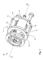
図1は、いくつかの実施形態に係るイオン源100の一例を示す斜視図である。図2は、図1に示されるイオン源100の断面斜視図である。例示される実施形態では、イオン源100は、全体として、内部イオン化チャンバ又は容積208を画定する本体104と、磁石アセンブリ112と、電子源116と、レンズアセンブリ120とを有している。
FIG. 1 is a perspective view illustrating an example of an
イオン源100は、イオン源軸124の周りに概ね配置される全体形状又は構成を有することができる。動作時に、イオン源100は、イオン源軸124に沿って電子ビームを生成し、かつイオン化されることになるサンプル材料の流れをイオン源軸124に対して任意の方向に受け入れることができる。分析されるサンプル材料は、複合技法を含む任意の適切な手段によって、イオン源100に導入することができ、その場合、サンプル材料は、例えば、ガスクロマトグラフィ(GC)機器等の分析分離機器の出力物となる。その後、イオン源100は、イオンを生成し、イオンをイオン源軸124に沿って集束させて、イオンビームにする。そのイオンは、イオン源軸124に沿ってイオン源100から出て、次のイオン処理デバイスに入る。そのイオン処理デバイスは、イオン源軸124に沿ったイオンの入口を有することができる。
The
イオン化チャンバ208は、イオン源軸124に沿って第1の端部から第2の端部までの長さを有している。サンプル源から、サンプル材料を電子ビームと相互作用させるイオン化チャンバ208の中に向けてサンプル材料を誘導する経路を設けることに適した任意の場所には、本体104を貫通するようにサンプルの入口228が形成されている。イオン化チャンバ208の軸方向長さは、所望の被分析物分子をイオン化するために利用可能な比較的長い実用的な電子ビーム領域を設けるように選択することができ、それによって、イオン源100のイオン化効率を高め、その結果、全体としての機器の感度を高めることができる。
The
磁石アセンブリ112は、本体104を同軸上にて包囲している。磁石アセンブリ112は、イオン化チャンバ208内に均一な軸方向磁界を生成するように構成され、その磁界は、電子ビームと、結果として生成されたイオンビームとをイオン源軸124に沿って集束かつ圧縮する。磁気的に制限された電子ビーム及び比較的長いイオン化チャンバ208によって、イオン化チャンバ208から抽出し(放出し)、最終的に、例えば、質量分析器、又はイオンガイド、イオントラップ、質量フィルタ、衝突セル等の質量分析器に前置される別種類のデバイス等のような下流のイオン処理デバイスに受け入れることを改善するために十分に適したイオンビームが、生成可能となる。イオンビームは、ニーア型のイオン源にて生じることがわかっているイオン損失を被ることなく抽出することができる。なお、ニーア型のイオン源は、イオン化チャンバ208の内面との衝突時に多数のイオンがフィラメントに向かって引っ張られるか、又は集束から外れ、中和される(失われる)ものである。磁石アセンブリ112は、イオン源軸124の周りで円周方向にて互いに離れて位置する複数の磁石132を有することができる。例示される実施形態は、リング状のヨーク134に固定された4つの磁石132から成る対称的な配置関係を包含するものとなっている。磁石132は永久磁石又は電磁石とすることができる。サンプルの入口228と、電線管等の他の構成要素とは、隣接する磁石132における任意の対間の間隙に位置決めすることができる。磁石132は、間隙によって互いに離れて位置するが、イオン源軸124の周りに対称に配置されており、生成される軸方向磁界は均一となっている。
The
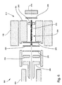
電子源116は、電子を生成し、イオン化チャンバ208を通して第1の端部から電子ビームを誘導するように構成される任意のデバイスとすることができる。例示される実施形態では、電子源116は1つ又は複数の陰極238を有している。陰極238は熱イオンを放出可能に構成されており、それゆえ、陰極238は、例えば、レニウム若しくはタングステン−レニウム合金等の熱イオン放出材料から構成される1つ若しくは複数のフィラメント(代替的には、コア上のコーティング)とすることができるか、又はそのようなフィラメントを有することができる。陰極238は、熱イオン放出を引き起こすのに十分な温度まで加熱されるようになっている。加熱は、通常、陰極238を通して電流を流すことによって行われる。その電流を調節することによって電子エネルギーを調節することができ、電子エネルギーは、通常、約70eVに設定されるが、それよりも低くても、高くてもよい。また、電子源116は、イオンリペラ240と、電子反射体244(プレート又は電極)とを有している。陰極238は、電子反射体244とイオンリペラ240との間に位置決めされ、その場所は、イオンリペラ240によってイオン化チャンバ208から分離された電子源領域と見なすことができる。イオンリペラ240(それは電子抽出器と見なすこともできる)は、イオン源軸124上に開口部を有する壁又はプレートとして構成することができる。電子エネルギーは、イオンリペラ240及び電子反射体244に印加される電圧によって設定される。電子反射体244に印加される電圧は、生成されたばかりの電子をレンズアセンブリ120に向かって加速させるようになっている。このために、電子反射体244と、後に説明されるレンズアセンブリ120の「抽出器」等のような陰極238の下流に位置する任意の適切な導電性素子(陽極)との間に、軸方向電圧勾配を掛けることができる。電子反射体244に印加される電圧は、通常では負値となっているが、より一般的には、リペラ240、及び後に説明されるレンズアセンブリ120の「第1のレンズ素子」までにおける他の下流光学系よりも低い正値となっている。電子反射体244及び陰極238が等電位にて動作可能に構成されているか、又は電子反射体244が、電子をイオン化チャンバ208の中に押し込むことを支援するために陰極238よりも高い負値とすることを可能とするように構成されている。
The
レンズアセンブリ120は、電子源116に対して軸方向の反対側に位置するイオン化チャンバ208の第2の端部に位置決めされている。レンズアセンブリ120は、数ある中でも、イオンビームをイオン化チャンバ208からイオン源軸124に沿って次のイオン処理デバイスの中に誘導するように構成されている。このために、レンズアセンブリ120は、電圧源によって独立して設定可能な複数のレンズ素子(又は電極)を有している。各レンズ素子はイオン源軸124上に開口部又はスロットを有することができる。例示される実施形態では、レンズアセンブリ120はイオン抽出レンズ(又はイオン抽出器)248と、イオン源軸124に沿って抽出器248から離れて位置する第1のレンズ素子(又は電子反射体)250と、イオン源軸124に沿って第1のレンズ素子250から離れて位置する第2のレンズ素子(又はイオン反射体)252と、イオン源軸124に沿って第2のレンズ素子252から離れて位置するイオン源出口レンズ素子(又はイオンビーム集束レンズ素子)256とを有している。イオン源出口レンズ素子256は、イオン処理デバイスへの入口レンズ素子として構成することができるか、又はその役割を果たすこともできる。レンズアセンブリ120は、第2のレンズ素子252とイオン源出口レンズ素子256との間に1つ又は複数のさらなるイオン集束レンズ素子254を有することもでき、イオンビームを集束するために利用することができる。イオンリペラ240及び抽出器248は、イオン化チャンバ208の軸方向におけるそれぞれ第1の端部及び第2の端部と見なすことができる。当業者に理解されるように、イオン化チャンバ208からイオンビームを引き出すことを支援するために、抽出器248に適切な大きさの電圧を印加することができる。
The
第1のレンズ素子250は、イオン化チャンバ208の直ぐ外側に位置決めされ、チャンバの下流側に位置する抽出器248に直接隣接している。電子ビームを反射してイオン化チャンバ208の中に戻すために、第1のレンズ素子250に適切な大きさの電圧を印加することができる。従って、陰極238(又は陰極238及び電子反射体244)及び第1のレンズ素子250は、イオン源軸124に沿って電子ビームを反射し、イオン化チャンバ208を通して往復させるように協調して働き、これによって、イオン化チャンバ208内で被分析物のEIイオン化のために利用可能な電子密度を高めることとなる。
The
電子を反射してイオン化チャンバ208の中に戻すために、第1のレンズ素子250に相対的に大きな電圧を印加することができる。この結果、一般的に第1のレンズ素子250と抽出器248との間における領域内でイオンを生成することができ、その領域はイオントラッピング領域と呼ばれる場合がある。イオン化チャンバ208と比べて、この領域内のエネルギーは低く、それゆえ、この領域内で生成されたイオンは望ましくないほど低いイオンエネルギーとなるおそれがある。結果として、これらのイオンは、この領域内に捕捉される傾向となる。これらのイオンは本明細書にて「低エネルギー」又は「より低いエネルギーの」又は「捕捉された」イオンと呼ばれる場合があり、そのイオンは、この文脈において、イオン源100に対して意図された動作条件下で、トラッピング領域内に捕捉できるほど十分に低いエネルギーを有するイオンを指すものとする。これに対して、イオン化チャンバ208にて通常生成される「高エネルギー」又は「より高いエネルギーの」又は「捕捉されない」イオンは、レンズアセンブリ120を突き抜けて、下流のイオン処理デバイスに入ることができる。イオントラッピングは、望ましくない空間電荷を生じ、イオン電流を不安定にするおそれがあるので、結果として望ましくないような一定しない性能になる。
A relatively large voltage can be applied to the
第2のレンズ素子252は、第2のレンズ素子252と抽出器248との間における領域内のイオントラッピングを実質的に低減するか、又は解消するために設けられている。第2のレンズ素子252上に設定された電圧は、第1のレンズ素子250上に設定された電圧よりも高い正値とすることができる。結果として、第2のレンズ素子252は、低エネルギーイオンを反射して第1のレンズ素子250に向かって戻し、これらのイオンはその後第1のレンズ素子250と衝突して中和されることとなる。さらに、第1のレンズ素子250は、トラッピング領域内のイオントラッピングを最小化するように、実行可能な限り抽出器248の近くに位置決めすることができる。
The
図3は、イオンシミュレーションソフトウェアによって作成されたイオン源300のモデルを示している。このモデルは、イオン源300の側断面図に対応するものである。イオン源300は、上記で説明され、かつ図1及び図2にて示されるイオン源100に概ね類似しており、従って、類似の構成要素は類似する符号によって示されている。このモデルは、出口レンズ素子256の直ぐ下流に位置し、かつイオン源300との軸上に位置決めされる無線周波数(RF)四重極質量フィルタ360を有している。図3は、イオン源軸に沿って集中した強い電子ビーム362を示しており、電子は反射して陰極238と第1のレンズ素子250との間を往復するようになっている。このシミュレーションでは、磁界強度は750ガウスとなっている。実際には、それよりも強い磁界強度又は弱い磁界強度が用いられる場合もある。
FIG. 3 shows a model of the
また、図3は、イオン化チャンバ208の少なくとも一部364(本体104の1つ又は複数の内面によって画定される部分等)を、先細り形状又は円錐形状とし、かつレンズアセンブリ120の方向に発散する実施形態もまた示している。すなわち、イオン化チャンバ208の断面積は、レンズアセンブリ120の方向にて徐々に大きくなっている。この変化する形状は電界を僅かに減衰させ、これによって、イオンがレンズアセンブリ120及び後続のイオン処理デバイスの方向に優先的に進行可能となる。
Also, FIG. 3 illustrates an implementation in which at least a
図4は、図3と同じモデルを示すが、イオン源軸に沿って制限されたイオンビーム466を含むようなイオンの軌跡を示している。図5は、レンズアセンブリ120の周囲の領域を示す拡大図である。イオントラッピング領域が、円568によって示されている。低エネルギーイオン470が、図4及び図5に示されており、第2のレンズ素子252から反射されて、第1のレンズ素子250に衝突するようになっている。図4及び図5では、本明細書にて開示されるイオン源が、イオン源内のイオン容積内で生成された高いエネルギーのイオンを高い効率で送り出すことを維持しながら、イオントラッピングを著しく低減するか、又は解消することができることが実証されている。図3〜図5のイオン源300は、円錐形のイオン容積形状を用いてモデル化されたが、他のモデルが図2に示されるような直線内腔(一定の内径)形状を用いてシミュレートされて、同様の結果が生成されたということに留意されたい。
FIG. 4 shows the same model as FIG. 3, but showing an ion trajectory that includes an
別の実施形態では、軸方向磁界を変更して、電子ビームと、その後に生成されるイオンビームとを所望の形態に整形することができる。これは、例えば、磁石アセンブリの構成を変更することによって達成することができる。図6は、別の実施形態にて、軸方向電子ビーム672及び磁石アセンブリ612を示しながら、イオンシミュレーションソフトウェアによって作成されたイオン源600の別のモデルを示している。イオン源軸に対して径方向に位置決めされた磁石(径方向磁石132)に加えて、磁石アセンブリ612は、後方又は軸上磁石674を有している。軸上磁石674は、イオン源軸上にて、電子反射体244から見てイオン化チャンバ208とは反対側に位置するイオン化チャンバ208の外部にて位置決めされる。この例では、軸上磁石674は円板形になっており、イオン源軸がその中心を通り抜けるようになっている。軸上磁石674を加えると、電子ビーム672は電子源にてさらに集束され、レンズアセンブリ120の方向にて徐々に広がるか、又は発散するようになっている。電子ビーム672の包絡線を広げることによって、より大きなイオン化領域が生成され、イオン化確率を改善することができる。このことは、イオン化プロセスに及ぼす空間電荷の悪影響に対処することに有用な場合がある。
In another embodiment, the axial magnetic field can be altered to shape the electron beam and the subsequently generated ion beam into the desired form. This can be accomplished, for example, by changing the configuration of the magnet assembly. FIG. 6 illustrates another model of an
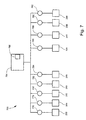
図7は、本明細書にて開示されるようなイオン源を設けることができるハードウェア又は電子機器700の一例を示す概略図である。イオン源の種々の構成要素に印加される個々の電圧は、それぞれ符号の776〜792として表されている(それは本明細書にて総称的に電源又は電圧源と呼ばれる場合がある)。いくつかの実施形態では、1つ又は複数の電圧786が本体104の1つ又は複数の導電性素子に印加される場合がある。電圧源776〜792の内1つ又は複数の電圧源のパラメータをコントローラ794によって制御できることを示すために、電圧源776〜792はコントローラ794(例えば、電子プロセッサに基づくコントローラ又はコンピュータ)と信号通信するように示されている。パラメータは、例えば、電圧の大きさの設定及び調節;印加される電圧のオン/オフ状態、タイミング及び持続時間;電圧源776〜792の内2つ以上の電圧源に対する電圧印加の協調又は同期等を含むことができる。コントローラ794は、電圧源776〜792のプログラミングされた制御を実施するためにコンピュータ読み取り可能媒体又はソフトウェア796を含むことができる。いくつかの実施形態では、コントローラ794は、本明細書にて開示される方法の内1つ又は複数を、全体的に又は部分的に実施することができる(例えば、ファームウェア及び/又はソフトウェアを利用する)。
FIG. 7 is a schematic diagram illustrating an example of hardware or
いくつかの実施形態では、電子放出を開始するときに、「初期」電子エネルギーは、熱イオン陰極238とイオンリペラ240との間における電位差として設定することができる。陰極238又はイオンリペラ240上の電圧が変化しても、他の構成要素上の電圧を調節することによって、この電位差を所望の固定値に維持することができる。例えば、電子反射体244上の電圧に追従するように陰極238上の電圧を調節することによって、適切な電子エネルギーのオフセット量を依然として維持しながら、イオンリペラ240をランプ制御し、最適化することができる。さらに、第1のレンズ素子250上の電圧は、陰極電圧に追従し、第1のレンズ素子250の電子反射機能を最適化することができる。追従機能は、例えば、図7にて概略的に示されるコントローラ794によって実施することができる。デフォルト動作として、コントローラ794は、陰極電圧を読み取って、同じ値を第1のレンズ素子250に印加することができる。第1のレンズ素子250の最適化をさらに改善できるようにするために、さらなる印加オフセット電圧をランプ制御し、デフォルト印加陰極整合電圧と加算することができる。すなわち、VFIRST LENS ELEMENT=VCATHOD+VOFFSETである。オフセット電圧を印加することによって、第1のレンズ素子250により強い電子反射をもたらし、第1のレンズ素子250と抽出器248との間におけるイオントラッピング領域への電子の流入を最小化することができ、これによって、より実用的な高エネルギーイオンの量をさらに増やし、望ましくない低エネルギーイオンの量をさらに減らすことができる。同様に、電子エネルギーのランプ制御が陰極電圧を変更し、第1のレンズ素子250に印加される電圧もランプ制御される陰極電圧に十分に追従することができる。
In some embodiments, the “initial” electron energy can be set as a potential difference between the
いくつかの応用形態では、イオン源にて生じる電子空間電荷の効果を低減するか、又は解消することが望ましい場合がある。例えば、空間電荷効果は、電子ビームを制御不可能に変調させ、これによって、イオンビームの安定性に悪影響を及ぼすほど著しい場合がある。これに対処するために、いくつかの実施形態では、電子源116、レンズアセンブリ120、及び/又は本体104の導電性素子の内1つ又は複数に周期的な電圧を印加することができる。周期的な電圧は周期的なDCパルス(実験的に最適化されたパルス幅、周期及び振幅を有する)、又は高周波(例えば、RF)電位とすることができる。周期的な電圧は、汚染物質のレベルが上昇することから生じる望ましくない任意の表面電荷蓄積を放電することができる。代替的には、例えば、適切な電子光学系を利用して、電子ビームをイオン源軸から離れるように周期的に偏向させること等によって、電子ビームをゲート制御して空間電荷蓄積を軽減することができる。いくつかの実施形態では、空間電荷効果は、米国特許第7,291,845号にて開示される技法を実施することによって対処することができ、その内容全体が引用することにより本明細書の一部を成すものとする。
In some applications, it may be desirable to reduce or eliminate the effect of electron space charge that occurs in the ion source. For example, the space charge effect may be so severe that it uncontrollably modulates the electron beam, thereby adversely affecting the stability of the ion beam. To address this, in some embodiments, a periodic voltage can be applied to one or more of the
図8は、別の実施形態について、図1及び図2に示されるイオン源100の一部の概略図である。この実施形態では、陰極(フィラメント)238とイオンリペラ240との間にて、電子源116にさらなる電極(又は電子抽出器)802が追加されている。特に低い電子エネルギー(例えば、9eV〜25eV)にて動作しているときに、電子抽出器802に適切な電圧を印加することによって、電子抽出器802を利用して電子源116内の電界条件を調節することができる。例えば、電子抽出器802は、電子を陰極238から引き離し、イオン化チャンバ208に向かって引き寄せ、イオン源の本体104とイオンリペラ240との間における電位差を低くしておくことを支援することができる。
FIG. 8 is a schematic diagram of a portion of the
図9は、本明細書にて開示されるようなイオン源100を設けることができる質量分析(MS)システム900の一例を示す概略図である。そのMSシステム900は、全体として、サンプル源902と、イオン源100と、質量分析計(MS)906と、イオン源100及びMS906の内部を制御された減圧レベルに保持する真空システムとを有している。真空システムは、イオン源100及びMS906からそれぞれ続く真空ライン908及び910によって概略的に示されている。真空ライン908,910は、当業者によって理解される1つ又は複数の真空生成ポンプ及び関連する配管系統及び他の構成要素を概略的に表している。イオン源100とMS906との間に1つ又は複数の他のタイプのイオン処理デバイス(図示せず)が設けられる場合があることも理解されるであろう。種々のタイプのサンプル源、分析計、及び関連する構成要素における構造及び動作は当業者によって一般的に理解されており、それゆえ、本明細書にて開示される主題を理解するために必要に応じて簡略的にのみ説明されている。実際には、イオン源100はMS906と一体に構成することができるか、そうでない場合には、MS906の前端又は入口と見なすことができ、それゆえ、実施形態によってはMS906の構成要素と見なされる場合がある。
FIG. 9 is a schematic diagram illustrating an example of a mass spectrometry (MS)
サンプル源902は、分析されるサンプルをイオン源100に供給するための任意のデバイス又はシステムとすることができる。サンプルは、サンプル源902からイオン源100に流れ込む気相又は蒸気の形で与えることができる。ガスクロマトグラフィ−質量分析(GC−MS)システム等の複合システムでは、サンプル源902はGCシステムとすることができ、その場合、GCシステムの分析カラムが、適切なハードウェアを通して、イオン源100とのインターフェースを構成することとなる。
MS906は、全体として、ハウジング916内に封入される質量分析器912及びイオン検出器914を含むことができる。真空ライン910は質量分析器912の内部を非常に低い(真空)圧力に維持するようになっている。いくつかの実施形態では、質量分析器912の圧力は10−4Torr〜10−9Torrに及ぶようになっている。真空ライン910は、MS906から任意の残留非分析中性分子を除去することもできる。質量分析器912は、それぞれのm/z比に基づいて被分析物イオンを分離するか、選別するか、又はフィルタリングするように構成される任意のデバイスとすることができる。質量分析器の例は、限定はしないが、多重極電極構造(例えば、四重極質量フィルタ、イオントラップ等)、飛行時間(TOF)分析器、イオンサイクロトロン共鳴(ICR)トラップを含む。質量分析器912は、特にイオンフラグメンテーション分析が望まれるときに、2つ以上の質量分析器から成るシステムを含むことができる。例として、質量分析器912は、当業者によって理解されるような、タンデムMS又はMSnシステムとすることができる。別の例として、質量分析器912は、質量フィルタと、それに続く衝突セルとを含むことができ、さらに、それに質量フィルタ(例えば、三重極又はQQQシステム)又はTOFデバイス(例えば、qTOFシステム)が続く。イオン検出器914は、質量分析器912から出力された質量弁別後のイオンの流速(又は流れ)を収集し、測定するように構成される任意のデバイスとすることができる。イオン検出器914の例は、限定はしないが、電子増倍管、光電子増倍管、及びファラデーカップを含んでいる。
The
本明細書にて開示されるような軸方向EI源は、いくつかの実施形態では、高電子エネルギー又は低電子エネルギーのいずれかで動作することができる。電子ビームのエネルギーは、フィラメントに印加される電圧を調節し、それによって、フィラメントに流れる電流を調節することができる。いくつかの実施形態では、電子ビームは、9eV〜150eVの範囲に渡って調節することができる。70eV未満の電子エネルギー、例えば、9eV〜25eVの範囲内の電子エネルギーは、ソフトイオン化方式の範囲内にあると見なすことができる。本明細書にて開示されるような軸方向EI源は、これらの電子エネルギー範囲に渡ってEIを実効的に実施することができる。非常に低いエネルギーであっても、そのEI源は、多くの実験にとって十分な強度及びイオン化収量を有する電子ビームを生成することができる。それゆえ、これらの軸方向EI源はハードイオン化又はソフトイオン化を実施することができ、所与の被分析物又は1組の被分析物のイオン化及び質量分析プロセスを最適化するために、所望により、又は必要に応じて、ハードイオン化とソフトイオン化とを切り替えることができる(同じ実験中を含む)。それゆえ、その軸方向EI源は、従来、化学イオン化(CI)等の従来のソフトイオン化を選択してEIが放棄される数多くの場合に利用することができる。従って、本明細書にて開示されるような軸方向EI源は、CI源及び従来のEI源等の他のデバイスと比較して、より万能なイオン化デバイスとすることができる。例えば、軸方向EI源は、分子イオン又は他の高質量イオンの形成等の望ましいイオン化経路に好都合である低い電子エネルギーにおいて動作することができる。低い電子エネルギーにおける軸方向EI源の動作に関連する方法が、本願と同時に出願され、かつ「ELECTRON IONIZATION (EI) UTILIZING DIFFERENT EI ENERGIES」と題する米国特許出願(代理人整理番号第20120352−01号、米国特許出願番号13/925,470)に開示されており、その内容全体が引用することにより本明細書の一部を成すものとする。 An axial EI source as disclosed herein can operate with either high or low electron energy in some embodiments. The energy of the electron beam can adjust the voltage applied to the filament, thereby adjusting the current flowing through the filament. In some embodiments, the electron beam can be adjusted over a range of 9 eV to 150 eV. Electron energy less than 70 eV, for example electron energy in the range of 9 eV to 25 eV, can be considered to be in the soft ionization regime. An axial EI source as disclosed herein can effectively perform EI over these electron energy ranges. Even at very low energy, the EI source can produce an electron beam with sufficient intensity and ionization yield for many experiments. Therefore, these axial EI sources can perform hard ionization or soft ionization, optionally to optimize the ionization and mass spectrometry process of a given analyte or set of analytes. Or, if necessary, hard ionization and soft ionization can be switched (including during the same experiment). Therefore, the axial EI source can be utilized in many cases where EI is abandoned by selecting traditional soft ionization, such as chemical ionization (CI). Thus, an axial EI source as disclosed herein can be a more versatile ionization device compared to other devices such as CI sources and conventional EI sources. For example, an axial EI source can operate at low electron energies that favor the desired ionization pathway, such as the formation of molecular ions or other high mass ions. A method related to the operation of an axial EI source at low electron energy is filed at the same time as the present application and is entitled “ELECTRON IONIZATION (EI) UTILIZING DIFFERENT EI ENERGIES” (Attorney Docket No. 20120352-01, US patent application Ser. No. 13 / 925,470), the entire contents of which are hereby incorporated by reference.
イオン源の例が、これまで主にEIと関連して説明されたが、それに加えて、又はその代わりに、本明細書にて教示されるイオン源が、同じく電子ビームを利用する既知の技法である化学イオン化(CI)用に構成できることは理解されよう。CIの場合、そのイオン源はイオン化チャンバに反応性ガスを入れるための入口を含むことができる。 Although examples of ion sources have been described so far primarily in connection with EI, in addition to or instead of the ion sources taught herein are known techniques that also utilize an electron beam. It will be appreciated that it can be configured for chemical ionization (CI). In the case of CI, the ion source can include an inlet for entering reactive gas into the ionization chamber.
例示的な実施形態:
ここで開示されている主題により提供される例示的な実施形態は、以下を含むが、これらに限定されない。
Exemplary embodiments:
Exemplary embodiments provided by the subject matter disclosed herein include, but are not limited to:
実施形態1.イオン源が、
イオン化チャンバ、及びイオン化チャンバに繋がるサンプルの入口を有する本体であって、イオン化チャンバに第1の端部及び第2の端部を設けており、イオン源軸に沿って第1の端部から第2の端部までの長さを有する本体と、
本体を包囲し、かつイオン化チャンバ内に軸方向磁界を生成するように構成される磁石アセンブリと、
第1の端部に位置決めされ、かつ熱イオン陰極及び電子反射体を有する電子源であって、電子ビームを、イオン化チャンバを通してイオン源軸に沿って加速させるように構成される電子源と、
第2の端部に位置決めされる抽出器、イオン化チャンバの外部に設けられ、かつイオン源軸に沿って抽出器から離れて位置する第1のレンズ素子、及びイオン源軸に沿って第1のレンズ素子から離れて位置する第2のレンズ素子を有するレンズアセンブリであって、抽出器が、イオン化チャンバからイオン源軸に沿ってイオンビームを外部に誘導するように構成され、第1のレンズ素子が、電子ビームを電子源に向かって反射するように構成され、第2のレンズ素子が、低エネルギーのイオンを第1のレンズ素子に向かって反射しながら高エネルギーのイオンを送り出すように構成される、レンズアセンブリと
を備えている。
Embodiment 1. FIG. The ion source
A main body having an ionization chamber and a sample inlet connected to the ionization chamber, wherein the ionization chamber has a first end and a second end, and the first end from the first end along the ion source axis. A body having a length up to two ends;
A magnet assembly that surrounds the body and is configured to generate an axial magnetic field in the ionization chamber;
An electron source positioned at a first end and having a thermionic cathode and an electron reflector, the electron source configured to accelerate an electron beam along an ion source axis through an ionization chamber;
An extractor positioned at the second end, a first lens element disposed outside the ionization chamber and positioned away from the extractor along the ion source axis, and a first along the ion source axis A lens assembly having a second lens element located away from the lens element, wherein the extractor is configured to direct an ion beam out of the ionization chamber along the ion source axis, the first lens element Is configured to reflect the electron beam toward the electron source, and the second lens element is configured to emit high energy ions while reflecting the low energy ions toward the first lens element. And a lens assembly.
実施形態2.実施形態1に係るイオン源にて、イオン化チャンバは、長さに沿って一定である断面積を有するか、又は長さの少なくとも一部に沿って増加する断面積を有している。 Embodiment 2. FIG. In the ion source according to embodiment 1, the ionization chamber has a cross-sectional area that is constant along the length or has a cross-sectional area that increases along at least a portion of the length.
実施形態3.実施形態1又は実施形態2に係るイオン源にて、磁石アセンブリは、イオン源軸の周りで円周方向にて互いに離れて位置する複数の磁石を備えている。 Embodiment 3. FIG. In the ion source according to the first embodiment or the second embodiment, the magnet assembly includes a plurality of magnets that are positioned apart from each other in the circumferential direction around the ion source axis.
実施形態4.実施形態3のイオン源にて、サンプルの入口が2つの磁石の間に位置決めされている。 Embodiment 4 FIG. In the ion source of Embodiment 3, the sample inlet is positioned between two magnets.
実施形態5.実施形態3又は実施形態4に係るイオン源にて、磁石アセンブリが、イオン化チャンバの外部のイオン源軸上に位置決めされる軸上磁石であって、電子ビームを抽出器に向かう方向に発散させるように方向磁界を変更する構成である軸上磁石を備えている。 Embodiment 5. FIG. In an ion source according to embodiment 3 or embodiment 4, the magnet assembly is an on-axis magnet positioned on the ion source axis outside the ionization chamber so as to diverge the electron beam in the direction towards the extractor. Is provided with an on-axis magnet that is configured to change the directional magnetic field.
実施形態6.実施形態1〜実施形態5のいずれか一つに係るイオン源が、第1の端部にて陰極と抽出器との間に位置決めされるイオンリペラを備えている。 Embodiment 6. FIG. The ion source according to any one of Embodiments 1 to 5 includes an ion repeller that is positioned between the cathode and the extractor at the first end.
実施形態7.実施形態1〜実施形態6のいずれか一つに係るイオン源にて、レンズアセンブリは、第2のレンズ素子から離れて位置する出口レンズであって、イオンビームをイオン源軸に沿ってイオン処理デバイスの中に誘導するように構成される出口レンズを備える。 Embodiment 7. FIG. In the ion source according to any one of Embodiments 1 to 6, the lens assembly is an exit lens positioned away from the second lens element, and the ion beam is ion-treated along the ion source axis. An exit lens configured to guide into the device.
実施形態8.実施形態1〜実施形態7のいずれか一つに係るイオン源が、電子源及びレンズアセンブリと信号通信する電圧源と、電圧源の動作を制御するように構成されるコントローラとを備え、
動作は、
陰極に印加される電圧を調節するプロセスと、
陰極に印加される電圧を調節しながら、陰極、並びに第1の端部にて陰極及び抽出器間に位置決めされたイオンリペラの間における一定の電位差を維持するプロセスと、
陰極に印加される電圧に対する調節に基づいて、第1のレンズ素子に印加される電圧を調節するプロセスと、
陰極及び第1のレンズ素子に印加される電圧を、陰極及び第1のレンズ素子間で電子ビームの反射を維持することに十分なそれぞれの値に設定するプロセスと、
陰極及び第1のレンズ素子に印加される電圧を、陰極及び第1のレンズ素子間で電子ビームの反射を維持することに十分なそれぞれの値に設定するとともに、第1のレンズ素子に陰極に対するオフセット電圧を加え、第1のレンズ素子からの電子ビームの反射を高めるプロセスと、
第2のレンズ素子に印加される電圧を、第2のレンズ素子及び抽出器間に捕捉されたイオンを第1のレンズ素子に向かって加速させることに十分な値に設定するプロセスと、
電子源の導電性素子にパルス電圧を印加するプロセスと、
レンズアセンブリの導電性素子にパルス電圧を印加するプロセスと、
本体にパルス電圧を印加するプロセスと、
電子ビームをゲート制御するプロセスと、
上記プロセスの内2つ以上のプロセスと
から成る群から選択されるものとなっている。
Embodiment 8. FIG. An ion source according to any one of Embodiments 1-7 comprises a voltage source in signal communication with the electron source and the lens assembly, and a controller configured to control the operation of the voltage source,
The operation is
Adjusting the voltage applied to the cathode;
Maintaining a constant potential difference between the cathode and an ion repeller positioned between the cathode and extractor at the first end while adjusting the voltage applied to the cathode;
Adjusting the voltage applied to the first lens element based on adjustment to the voltage applied to the cathode;
A process for setting a voltage applied to the cathode and the first lens element to respective values sufficient to maintain reflection of the electron beam between the cathode and the first lens element;
The voltages applied to the cathode and the first lens element are set to values sufficient to maintain the reflection of the electron beam between the cathode and the first lens element, and the first lens element is applied to the cathode. Applying an offset voltage to increase the reflection of the electron beam from the first lens element;
Setting the voltage applied to the second lens element to a value sufficient to accelerate ions trapped between the second lens element and the extractor toward the first lens element;
Applying a pulse voltage to the conductive element of the electron source;
Applying a pulse voltage to the conductive element of the lens assembly;
A process of applying a pulse voltage to the body;
A process to gate the electron beam;
It is selected from the group consisting of two or more of the above processes.
実施形態9.実施形態1〜実施形態8のいずれか一つに係るイオン源が、陰極及びイオン化チャンバ間におけるイオンリペラと、陰極及びイオンリペラ間における電子抽出器とを備えている。 Embodiment 9. FIG. The ion source according to any one of Embodiments 1 to 8 includes an ion repeller between the cathode and the ionization chamber, and an electron extractor between the cathode and the ion repeller.
実施形態10.イオン処理システムが、実施形態1〜実施形態9のいずれか一つに係るイオン源と、レンズアセンブリと通信するイオン処理デバイスとを備えている。 Embodiment 10 FIG. The ion processing system includes an ion source according to any one of Embodiments 1 to 9 and an ion processing device in communication with the lens assembly.
実施形態11.実施形態10に係るイオン処理システムにて、イオン処理デバイスは、イオンガイド、イオントラップ、質量フィルタ、衝突セル、及び質量分析器から成る群から選択される。 Embodiment 11. FIG. In the ion processing system according to the tenth embodiment, the ion processing device is selected from the group consisting of an ion guide, an ion trap, a mass filter, a collision cell, and a mass analyzer.
実施形態12.実施形態10に係るイオン処理システムが、質量分析器を備え、質量分析器と通信するイオン検出器をさらに備えている。 Embodiment 12 FIG. The ion processing system according to the tenth embodiment further includes an ion detector that includes a mass analyzer and communicates with the mass analyzer.
実施形態13.電子イオン化を実行する方法が、
電子を、電子ビームとして電子源から、電子源及びレンズアセンブリ間にイオン源軸に沿った長さを有するイオン化チャンバを通して誘導するステップと、
イオン化チャンバに軸方向磁界をかけることによってイオン源軸に沿って電子ビームを集束させるステップと、
電子源及びレンズアセンブリ間でイオン源軸に沿って往復させるように電子を反射させるステップと、
サンプル材料を電子ビームに向かってイオン化チャンバに送り込むことによってイオンを生成する生成ステップであって、イオンをイオン源軸に沿って集束してイオンビームとする生成ステップと、
レンズアセンブリを通してイオン源軸に沿ってイオンを送り出すステップと、
レンズアセンブリ内に捕捉されたイオンを反射させ、捕捉されていないイオンをレンズアセンブリから送り出しながら、捕捉されたイオンがレンズアセンブリから出ることを防ぐようになっているステップと
を含んでいる。
Embodiment 13. FIG. A method of performing electron ionization is
Directing electrons from the electron source as an electron beam through an ionization chamber having a length along the ion source axis between the electron source and the lens assembly;
Focusing the electron beam along the ion source axis by applying an axial magnetic field to the ionization chamber;
Reflecting the electrons back and forth between the electron source and the lens assembly along the ion source axis;
A generation step of generating ions by feeding sample material toward an electron beam into an ionization chamber, wherein the ions are focused along an ion source axis into an ion beam; and
Pumping ions along the ion source axis through a lens assembly;
Reflecting ions trapped within the lens assembly and delivering untrapped ions from the lens assembly while preventing the trapped ions from exiting the lens assembly.
実施形態14.実施形態13に係る方法が、軸方向磁界をかける際に利用される2つの磁石間にサンプル材料を誘導するステップをさらに含んでいる。 Embodiment 14 FIG. The method according to embodiment 13 further includes inducing sample material between two magnets utilized in applying an axial magnetic field.
実施形態15.実施形態13又は実施形態14に係る方法にて、電子を集束させるステップが、イオン源軸の周りで円周方向にて互いに離れて位置する複数の磁石を利用するプロセスを含む。 Embodiment 15. FIG. In the method according to embodiment 13 or embodiment 14, the step of focusing the electrons comprises a process utilizing a plurality of magnets positioned circumferentially around the ion source axis in a circumferential direction.
実施形態16.実施形態13〜実施形態15のいずれか一つに係る方法にて、電子を集束させるステップが、電子ビームが抽出器に向かう方向において発散するように行われる。 Embodiment 16. FIG. In the method according to any one of Embodiments 13 to 15, the step of focusing the electrons is performed such that the electron beam diverges in the direction toward the extractor.
実施形態17.実施形態13〜実施形態16のいずれか一つに係る方法にて、電子を集束させるステップが、イオン源軸の周りで円周方向にて互いに離れて位置する複数の磁石と、イオン化チャンバの外部のイオン源軸上に位置決めされた軸上磁石とを利用するプロセスを含んでいる。 Embodiment 17. FIG. In the method according to any one of Embodiments 13 to 16, the step of focusing the electrons includes a plurality of magnets positioned circumferentially around the ion source axis and the outside of the ionization chamber. And an on-axis magnet positioned on the ion source axis.
実施形態18.実施形態13〜実施形態17のいずれか一つに係る方法にて、電子を生成するステップは、陰極に電圧を印加することによって行われ、電子を生成するステップは、電圧を調節することによって電子のエネルギーを調節するプロセスをさらに含んでいる。 Embodiment 18. FIG. In the method according to any one of Embodiments 13 to 17, the step of generating electrons is performed by applying a voltage to the cathode, and the step of generating electrons is performed by adjusting the voltage. It further includes the process of regulating the energy of the.
実施形態19.実施形態18に係る方法が、陰極上の電圧を調節しながら、陰極及びレンズアセンブリ間に位置決めされたイオンリペラ上の電圧を調節する調節ステップであって、陰極及びイオンリペラ間の一定の電位差を維持する調節ステップをさらに含んでいる。 Embodiment 19. FIG. Embodiment 18 is a method of adjusting a voltage on an ion repeller positioned between a cathode and a lens assembly while adjusting a voltage on the cathode, maintaining a constant potential difference between the cathode and the ion repeller. It further includes an adjustment step.
実施形態20.実施形態18又は実施形態19に係る方法が、レンズアセンブリのレンズ素子に電圧を印加する印加ステップであって、電子ビームを反射してイオン化チャンバの中に戻す印加ステップと、陰極上の電圧を調節しながら、レンズ素子上の電圧を同じ量だけ調節するステップとをさらに含んでいる。 Embodiment 20. FIG. A method according to embodiment 18 or embodiment 19 is an application step of applying a voltage to the lens elements of the lens assembly, the application step reflecting the electron beam back into the ionization chamber, and adjusting the voltage on the cathode However, the method further includes adjusting the voltage on the lens element by the same amount.
実施形態21.実施形態18〜実施形態20のいずれか一つに係る方法にて、電子を生成するステップは、陰極に電圧を印加することによって行われ、電子を生成するステップは、レンズアセンブリのレンズ素子に電圧を印加する印加プロセスであって、電子ビームを反射してイオン化チャンバの中に戻す印加プロセスをさらに含んでいる。 Embodiment 21. FIG. In the method according to any one of Embodiments 18 to 20, the step of generating electrons is performed by applying a voltage to the cathode, and the step of generating electrons is a voltage applied to the lens element of the lens assembly. And an application process for reflecting the electron beam back into the ionization chamber.
実施形態22.実施形態21に係る方法が、陰極及びレンズ素子に印加される電圧を、陰極及びレンズ素子間で電子の反射を維持することに十分なそれぞれの値に設定するステップをさらに含んでいる。 Embodiment 22. FIG. The method according to embodiment 21 further includes the step of setting the voltage applied to the cathode and lens elements to respective values sufficient to maintain electron reflection between the cathode and lens elements.
実施形態23.実施形態22に係る方法が、陰極及びレンズ素子に印加されるそれぞれの電圧を等しい値に設定するステップ、又は陰極に印加される電圧に対して所定のオフセット量分レンズ素子に印加される電圧を増加させて、レンズ素子における反射を増加させる増加ステップをさらに含む。 Embodiment 23. FIG. The method according to Embodiment 22 sets the voltages applied to the cathode and the lens element to equal values, or sets the voltage applied to the lens element by a predetermined offset amount with respect to the voltage applied to the cathode. The method further includes an increasing step of increasing to increase reflection at the lens element.
実施形態24.実施形態13〜実施形態23に係るいずれか一つに係る方法が、レンズアセンブリの抽出器に電圧を印加して、イオンをイオン化チャンバからレンズアセンブリに送り込むステップを含む。 Embodiment 24. FIG. The method according to any one of embodiments 13-23 includes applying a voltage to the extractor of the lens assembly to force ions from the ionization chamber to the lens assembly.
実施形態25.実施形態24に係る方法が、イオン化チャンバの外部に位置決めされたレンズアセンブリの第1のレンズ素子に電圧を印加して、抽出器を通して電子ビームをイオン化チャンバの中に反射させるステップをさらに含んでいる。 Embodiment 25. FIG. The method according to embodiment 24 further includes applying a voltage to the first lens element of the lens assembly positioned outside the ionization chamber to reflect the electron beam through the extractor into the ionization chamber. .
実施形態26.実施形態25に係る方法が、レンズアセンブリの第2のレンズ素子に電圧を印加して、捕捉されたイオンを反射させて、第1のレンズ素子に衝突させるステップをさらに含んでいる。 Embodiment 26. FIG. The method according to embodiment 25 further includes the step of applying a voltage to the second lens element of the lens assembly to reflect the trapped ions to collide with the first lens element.
実施形態27.実施形態13〜実施形態26のいずれか一つに係る方法が、レンズアセンブリのレンズ素子に電圧を印加して、捕捉されたイオンを反射させて、レンズアセンブリの別のレンズ素子に衝突させるステップをさらに含んでいる。 Embodiment 27. FIG. A method according to any one of embodiments 13 to 26, comprising applying a voltage to the lens element of the lens assembly to reflect the trapped ions to collide with another lens element of the lens assembly. In addition.
実施形態28.実施形態13〜実施形態27のいずれか一つに係る方法が、電子源の導電性素子にパルス電圧を印加するプロセスと、レンズアセンブリの導電性素子にパルス電圧を印加するプロセスと、イオン化チャンバの少なくとも一部を画定する本体にパルス電圧を印加するプロセスと、電子ビームをゲート制御するプロセスと、上記プロセスの内2つ以上のプロセスとから成る群から選択されたパルス処理を実行するステップをさらに含んでいる。 Embodiment 28. FIG. A method according to any one of embodiments 13 to 27 includes a process of applying a pulse voltage to the conductive element of the electron source, a process of applying a pulse voltage to the conductive element of the lens assembly, Performing a pulse treatment selected from the group consisting of a process of applying a pulse voltage to a body defining at least a portion, a process of gating an electron beam, and two or more of the above processes. Contains.
実施形態29.実施形態13〜実施形態28のいずれか一つに係る方法が、電子源の陰極から電子を放出するステップと、電子源の電子抽出器に電圧を印加することによって、放出された電子を陰極から引き離すステップとを含む。 Embodiment 29. FIG. Embodiment 13 The method according to any one of Embodiments 13 to 28 includes a step of emitting electrons from a cathode of an electron source, and applying a voltage to an electron extractor of the electron source, thereby discharging the emitted electrons from the cathode. Pulling apart.
実施形態30.実施形態29に係る方法にて、電子源及びイオン化チャンバ間に位置決めされるイオンリペラに電圧を印加することによってイオンを電子源から押し返すステップをさらに含んでいる。 Embodiment 30. FIG. The method according to embodiment 29 further includes pushing ions back from the electron source by applying a voltage to an ion repeller positioned between the electron source and the ionization chamber.
実施形態31.実施形態13〜実施形態30のいずれか一つに係る方法が、レンズアセンブリを通して、イオン源軸上に入口を備えるイオン処理デバイスの中にイオンを送り込むことを含む。 Embodiment 31. FIG. The method according to any one of embodiments 13-30 includes pumping ions through a lens assembly into an ion processing device with an inlet on the ion source axis.
実施形態32.実施形態13〜実施形態31のいずれか一つに係る方法が、イオン化チャンバの中にサンプル材料を誘導する前に、ガスクロマトグラフからサンプル材料を出力するステップをさらに含んでいる。 Embodiment 32. FIG. The method according to any one of embodiments 13-31 further includes outputting the sample material from the gas chromatograph prior to directing the sample material into the ionization chamber.
図7に概略的に示されるシステムコントローラ794は、イオン源の種々の機能的な態様を制御し、監視し、タイミングを取り、同期させ、及び/又は調節するように構成される1つ又は複数のモジュールを表すことができることは理解されるであろう。また、システムコントローラ794は、例えば、イオン測定信号を受信すること、及び必要に応じてデータ収集及び信号解析に関連する他のタスクを実行し、解析中のサンプルを特徴付ける質量スペクトルを生成することを含め、関連する質量分析システムの機能又は構成要素を制御するように構成される1つ又は複数のモジュールを表す場合もある。
The
全てのそのような目的のために、コントローラ794は、本明細書にて開示される方法のいずれかを実行する命令を含むコンピュータ読み取り可能媒体を含むことができる。コントローラ794は、有線又は無線通信リンクを介してイオン源の様々な構成要素と信号通信するように概略的に示されている。また、これらの目的のために、コントローラ794は、1つ又は複数の種類のハードウェア、ファームウェア、及び/又はソフトウェアと、1つ又は複数のメモリ及びデータベースとを含む場合がある。コントローラ794は、通常、全体的な制御を与える主電子プロセッサを含み、専用制御動作又は特定の信号処理タスクのために構成される1つ又は複数の電子プロセッサを含む場合がある。また、システムコントローラ794は、種々の構成要素に電圧を印加するために、必要に応じて、具体的には示されない全ての電圧源と、タイミングコントローラ、クロック、周波数/波形発生器とを概略的に表す場合もある。コントローラ794は、ユーザ入力デバイス(例えば、キーパッド、タッチスクリーン、マウス等)、ユーザ出力デバイス(例えば、ディスプレイ画面、プリンタ、可視指示体又は警告、可聴指示体又は警告等)、ソフトウェアによって制御されるグラフィカルユーザインターフェース(GUI)、電子プロセッサによって読み出し可能な媒体(例えば、ソフトウェアにて具現される論理命令、データ等)をロードするデバイス等のような1つ又は複数のタイプのユーザインターフェースデバイスを表す場合もある。コントローラ794は、コントローラ794の種々の機能を制御し、管理するオペレーティングシステム(例えば、Microsoft Windows(登録商標)ソフトウェア)を含む場合もある。
For all such purposes, the
本明細書にて用いられる場合に、「信号通信する」という用語は、2つ以上のシステム、デバイス、構成要素、モジュール、又はサブモジュールが、所定のタイプの信号経路を通って進行する信号を介して互いに通信することができることを意味することは理解されるであろう。それらの信号は、第1のシステム、デバイス、構成要素、モジュール又はサブモジュールと第2のシステム、デバイス、構成要素、モジュール又はサブモジュールとの間の信号経路に沿って第1のシステム、デバイス、構成要素、モジュール又はサブモジュールから第2のシステム、デバイス、構成要素、モジュール、又はサブモジュールに情報、電力、又はエネルギーを伝達可能とする通信信号、電力信号、データ信号、又はエネルギー信号とすることができる。信号経路は、物理的接続、電気的接続、磁気的接続、電磁的接続、電気化学的接続、光学的接続、有線接続、又は無線接続を含むことができる。また、信号経路は、第1のシステム、デバイス、構成要素、モジュール、又はサブモジュールと、第2のシステム、デバイス、構成要素、モジュール、又はサブモジュールとの間におけるさらなるシステム、デバイス、構成要素、モジュール、又はサブモジュールを含む場合もある。 As used herein, the term “signal communication” refers to a signal that two or more systems, devices, components, modules, or sub-modules travel through a predetermined type of signal path. It will be understood that it means that they can communicate with each other. The signals are transmitted along the signal path between the first system, device, component, module or submodule and the second system, device, component, module or submodule. A communication signal, power signal, data signal, or energy signal that enables information, power, or energy to be transferred from the component, module, or submodule to the second system, device, component, module, or submodule. Can do. The signal path can include a physical connection, an electrical connection, a magnetic connection, an electromagnetic connection, an electrochemical connection, an optical connection, a wired connection, or a wireless connection. The signal path may also include additional systems, devices, components, between the first system, device, component, module, or submodule and the second system, device, component, module, or submodule. There may be a module or a submodule.
概して、「連通する(通信する)(communicate)」及び「連通している(in...communication with)」(例えば、第1の構成要素が第2の構成要素と「連通する」又は「連通している)等の用語を、本明細書では、2つ以上の構成要素又は要素間の構造的、機能的、機械的、電気的、信号、光、磁気、電磁気、イオン、又は流体関係を示すように用いている。従って、1つの構成要素が第2の構成要素と連通すると言われることは、第1の構成要素と第2の構成要素との間に追加の構成要素が存在し、及び/又はそれらに動作的に関連するか若しくは関与する可能性を排除するようには意図されていない。 Generally, “communicate” and “in ... communication with” (eg, a first component “communication” or “communication” with a second component). Are used herein to refer to structural, functional, mechanical, electrical, signal, optical, magnetic, electromagnetic, ionic, or fluid relationships between two or more components or elements. Thus, when one component is said to be in communication with the second component, there is an additional component between the first component and the second component, And / or is not intended to exclude the possibility of being operatively related to or involved in them.
本発明の様々な態様又は詳細を、本発明の範囲から逸脱することなく変更することができることが理解されるであろう。さらに、上記説明は、単に例示の目的のものであって限定の目的のものではなく、本発明は特許請求の範囲によって規定されるものとなっている。 It will be understood that various aspects or details of the invention may be changed without departing from the scope of the invention. Furthermore, the above description is for illustrative purposes only and is not intended to be limiting. The present invention is defined by the claims.
Claims (10)
前記本体を包囲し、かつ前記イオン化チャンバ内に軸方向磁界を生成するように構成される磁石アセンブリと、
前記第1の端部に位置決めされ、かつ熱イオン陰極及び電子反射体を有する電子源であって、電子ビームを、前記イオン化チャンバを通して前記イオン源軸に沿って加速させるように構成される電子源と、
前記第2の端部に位置決めされる抽出器、前記イオン化チャンバの外部に設けられ、かつ前記イオン源軸に沿って前記抽出器から離れて位置する第1のレンズ素子、並びに前記イオン源軸に沿って前記第1のレンズ素子から離れて位置する第2のレンズ素子を有するレンズアセンブリであって、前記抽出器が、前記イオン化チャンバから前記イオン源軸に沿ってイオンビームを外部に誘導するように構成され、前記第1のレンズ素子が、前記電子ビームを前記電子源に向かって反射させるように構成され、前記第2のレンズ素子が、低エネルギーのイオンを前記第1のレンズ素子に向かって反射しながら高エネルギーのイオンを送り出すように構成される、レンズアセンブリと
を備えているイオン源。 A main body having an ionization chamber and a sample inlet connected to the ionization chamber, wherein the ionization chamber has a first end and a second end, and the first end along the ion source axis A body having a length from a portion to the second end;
A magnet assembly that surrounds the body and is configured to generate an axial magnetic field in the ionization chamber;
An electron source positioned at the first end and having a thermionic cathode and an electron reflector, the electron source configured to accelerate an electron beam along the ion source axis through the ionization chamber When,
An extractor positioned at the second end; a first lens element provided outside the ionization chamber and positioned away from the extractor along the ion source axis; and the ion source axis A lens assembly having a second lens element positioned along and away from the first lens element, wherein the extractor directs an ion beam out of the ionization chamber along the ion source axis And the first lens element is configured to reflect the electron beam toward the electron source, and the second lens element directs low-energy ions toward the first lens element. And a lens assembly configured to deliver high energy ions while being reflected.
前記イオン源軸の周りにて周方向に互いに離れて位置する複数の磁石と、
前記イオン化チャンバの外部における前記イオン源軸上に位置決めされる軸上磁石であって、前記電子ビームを前記抽出器に向かう方向に発散させるように前記軸方向磁界を変更する構成である軸上磁石と
のうち少なくとも一方を有している、請求項1又は2に記載のイオン源。 The magnet assembly comprises:
A plurality of magnets positioned circumferentially apart from each other around the ion source axis;
An on-axis magnet positioned on the ion source axis outside the ionization chamber and configured to change the axial magnetic field so as to diverge the electron beam in a direction toward the extractor. The ion source according to claim 1, comprising at least one of:
前記電圧源の動作を制御するように構成されるコントローラと
をさらに備え、
前記動作は、
前記陰極に印加される電圧を調節するプロセスと、
前記陰極に印加される電圧を調節しながら、前記陰極、並びに前記第1の端部にて前記陰極及び前記抽出器間に位置決めされたイオンリペラの間における一定の電位差を維持するプロセスと、
前記陰極に印加された電圧に対する調節に基づいて、前記第1のレンズ素子に印加された電圧を調節するプロセスと、
前記陰極及び前記第1のレンズ素子に印加される電圧を、前記陰極及び前記第1のレンズ素子間で前記電子ビームの反射を維持するのに十分なそれぞれの値に設定するプロセスと、
前記陰極及び前記第1のレンズ素子に印加される電圧を、前記陰極及び前記第1のレンズ素子間で前記電子ビームの反射を維持するのに十分なそれぞれの値に設定すると共に、前記第1のレンズ素子に前記陰極に対するオフセット電圧を加え、前記第1のレンズ素子からの前記電子ビームの反射を高めるプロセスと、
前記第2のレンズ素子に印加される電圧を、前記第2のレンズ素子及び前記抽出器間に捕捉されたイオンを前記第1のレンズ素子に向かって加速させるのに十分な値に設定するプロセスと、
前記電子源の導電性素子にパルス電圧を印加するプロセスと、
前記レンズアセンブリの導電性素子にパルス電圧を印加するプロセスと、
前記本体にパルス電圧を印加するプロセスと、
前記電子ビームをゲート制御するプロセスと、
前記複数のプロセスの内2つ以上のプロセスと
から成る群から選択されたものとなっている、請求項1〜4のいずれか一項に記載のイオン源。 A voltage source in signal communication with the electron source and the lens assembly;
A controller configured to control operation of the voltage source;
The operation is
Adjusting the voltage applied to the cathode;
Maintaining a constant potential difference between the cathode and an ion repeller positioned between the cathode and the extractor at the first end while adjusting a voltage applied to the cathode;
Adjusting the voltage applied to the first lens element based on an adjustment to the voltage applied to the cathode;
Setting the voltage applied to the cathode and the first lens element to respective values sufficient to maintain reflection of the electron beam between the cathode and the first lens element;
The voltages applied to the cathode and the first lens element are set to respective values sufficient to maintain the reflection of the electron beam between the cathode and the first lens element, and the first Applying a voltage offset to the cathode to the lens element to enhance reflection of the electron beam from the first lens element;
A process of setting the voltage applied to the second lens element to a value sufficient to accelerate ions trapped between the second lens element and the extractor toward the first lens element; When,
Applying a pulse voltage to the conductive element of the electron source;
Applying a pulse voltage to the conductive element of the lens assembly;
Applying a pulse voltage to the body;
A process of gating the electron beam;
The ion source according to any one of claims 1 to 4, wherein the ion source is selected from the group consisting of two or more processes among the plurality of processes.
前記イオン化チャンバに軸方向磁界を負荷することによってイオン源軸に沿って前記電子ビームを集束させる集束ステップと、
前記電子源及び前記レンズアセンブリ間にて前記イオン源軸に沿って往復させるように前記電子を反射させる電子反射ステップと、
サンプル材料を前記電子ビームに向かって前記イオン化チャンバに送り込むことによってイオンを生成する生成ステップであって、前記イオンを前記イオン源軸に沿って集束させてイオンビームとする生成ステップと、
前記レンズアセンブリを通して前記イオン源軸に沿って前記イオンを送り出すイオン送出ステップと、
前記レンズアセンブリ内に捕捉されたイオンを反射させるイオン反射ステップであって、捕捉されていないイオンを前記レンズアセンブリから送り出しながら、前記捕捉されたイオンが前記レンズアセンブリから出ることを防ぐようにするイオン反射ステップと
を含む電子イオン化を実行する方法。 Directing electrons from the electron source as an electron beam through an ionization chamber having a length along the ion source axis between the electron source and the lens assembly;
Focusing step for focusing the electron beam along an ion source axis by loading an axial magnetic field to the ionization chamber;
An electron reflecting step for reflecting the electrons to reciprocate between the electron source and the lens assembly along the ion source axis;
Generating to generate ions by feeding sample material toward the electron beam into the ionization chamber, wherein the ions are focused along the ion source axis into an ion beam; and
An ion delivery step of delivering the ions along the ion source axis through the lens assembly;
An ion reflection step for reflecting ions trapped within the lens assembly, wherein the ions are sent out of the lens assembly to prevent the trapped ions from exiting the lens assembly A method of performing electron ionization comprising a reflection step.
前記生成ステップは、
前記電圧を調節することによって前記電子のエネルギーを調節するプロセスと、
前記電圧を調節することによって前記電子のエネルギーを調節するプロセスであって、前記陰極の電圧を調節しながら、前記陰極と、前記陰極及び前記レンズアセンブリ間に位置決めされたイオンリペラとの間における一定の電位差を維持するように、前記イオンリペラの電圧を調節するプロセスと、
前記電圧を調節することによって前記電子のエネルギーを調節し、かつ前記電子ビームを反射させて前記イオン化チャンバの中に戻すように、前記レンズアセンブリのレンズ素子に電圧を印加するプロセスであって、前記陰極の電圧を調節しながら、前記レンズ素子の電圧を同じ量だけ調節するプロセスと、
前記電子ビームを反射させて前記イオン化チャンバの中に戻すように、前記レンズアセンブリのレンズ素子に電圧を印加するプロセスと、
前記電子ビームを反射させて前記イオン化チャンバの中に戻すように、前記レンズアセンブリのレンズ素子に電圧を印加するプロセスであって、前記陰極及び前記レンズ素子に印加される電圧を、前記陰極及び前記レンズ素子間にて前記電子の反射を維持するのに十分なそれぞれの値に設定するプロセスと、
前記電子ビームを反射させて前記イオン化チャンバの中に戻すように、前記レンズアセンブリのレンズ素子に電圧を印加し、かつ前記陰極及び前記レンズ素子に印加される電圧を、前記陰極及び前記レンズ素子間にて前記電子の反射を維持するのに十分なそれぞれの値に設定するプロセスであって、前記陰極及び前記レンズ素子に印加される前記それぞれの電圧を等しい値に設定するか、又は前記レンズ素子における反射を増加させるように、前記陰極に印加される前記電圧に対して所定のオフセット量分前記レンズ素子に印加される前記電圧を増加させるプロセスと
のうち少なくとも1つを含む請求項6〜8のいずれか一項に記載の方法。 The generating step is performed by applying a voltage to the cathode,
The generating step includes
Adjusting the energy of the electrons by adjusting the voltage;
Adjusting the energy of the electrons by adjusting the voltage, the constant being between the cathode and an ion repeller positioned between the cathode and the lens assembly while adjusting the voltage of the cathode . Adjusting the voltage of the ion repeller to maintain a potential difference;
Adjusting the energy of the electrons by adjusting the voltage and applying a voltage to the lens elements of the lens assembly to reflect the electron beam back into the ionization chamber, the method comprising: Adjusting the voltage of the lens element by the same amount while adjusting the cathode voltage;
Applying a voltage to a lens element of the lens assembly to reflect the electron beam back into the ionization chamber;
A process of applying a voltage to a lens element of the lens assembly to reflect the electron beam back into the ionization chamber, the voltage applied to the cathode and the lens element being the cathode and A process of setting each value sufficient to maintain reflection of the electrons between lens elements;
A voltage is applied to the lens element of the lens assembly to reflect the electron beam back into the ionization chamber and the voltage applied to the cathode and the lens element is between the cathode and the lens element. A process of setting each value sufficient to maintain the reflection of the electrons, wherein each voltage applied to the cathode and the lens element is set to an equal value, or the lens element And / or increasing the voltage applied to the lens element by a predetermined offset relative to the voltage applied to the cathode to increase reflection at the cathode. The method as described in any one of.
前記イオンを前記イオン化チャンバから前記レンズアセンブリに送り込むように、前記レンズアセンブリの抽出器に電圧を印加する印加ステップであって、前記抽出器を通して前記電子ビームを前記イオン化チャンバの中に反射させるように、前記イオン化チャンバの外部に位置決めされた前記レンズアセンブリの第1のレンズ素子に電圧を印加する印加ステップと、
前記イオンを前記イオン化チャンバから前記レンズアセンブリに送り込むように、前記レンズアセンブリの抽出器に電圧を印加する印加ステップであって、前記抽出器を通して前記電子ビームを前記イオン化チャンバの中に反射させるように、前記イオン化チャンバの外部に位置決めされた前記レンズアセンブリの第1のレンズ素子に電圧を印加し、かつ前記捕捉されたイオンを反射させて前記第1のレンズ素子に衝突させるように、前記レンズアセンブリの第2のレンズ素子に電圧を印加する印加ステップと、
前記捕捉されたイオンを反射させて前記レンズアセンブリの別のレンズ素子に衝突させるように、前記レンズアセンブリのレンズ素子に電圧を印加する印加ステップと、
前記電子源の導電性素子にパルス電圧を印加するプロセスと、前記レンズアセンブリの導電性素子にパルス電圧を印加するプロセスと、前記イオン化チャンバの少なくとも一部を画定する本体にパルス電圧を印加するプロセスと、前記電子ビームをゲート制御するプロセスと、前記複数のプロセスの内2つ以上のプロセスとから成る群から選択されたパルス処理を実行する実行ステップと
のうち少なくとも1つをさらに含む請求項6〜9のいずれか一項に記載の方法。 Applying a voltage to an extractor of the lens assembly so as to deliver the ions from the ionization chamber to the lens assembly;
An applying step of applying a voltage to an extractor of the lens assembly to deliver the ions from the ionization chamber to the lens assembly so as to reflect the electron beam through the extractor into the ionization chamber. Applying a voltage to a first lens element of the lens assembly positioned outside the ionization chamber;
An applying step of applying a voltage to an extractor of the lens assembly to deliver the ions from the ionization chamber to the lens assembly so as to reflect the electron beam through the extractor into the ionization chamber. Applying a voltage to a first lens element of the lens assembly positioned external to the ionization chamber and reflecting the captured ions to impinge on the first lens element. Applying a voltage to the second lens element of
Applying a voltage to a lens element of the lens assembly so that the trapped ions are reflected and collide with another lens element of the lens assembly;
A process of applying a pulse voltage to the conductive element of the electron source, a process of applying a pulse voltage to the conductive element of the lens assembly, and a process of applying a pulse voltage to a body defining at least a portion of the ionization chamber And a step of performing a pulse process selected from the group consisting of two or more processes of the plurality of processes, and a gate control of the electron beam. The method as described in any one of -9.
Applications Claiming Priority (2)
| Application Number | Priority Date | Filing Date | Title |
|---|---|---|---|
| US13/925,623 US9117617B2 (en) | 2013-06-24 | 2013-06-24 | Axial magnetic ion source and related ionization methods |
| US13/925,623 | 2013-06-24 |
Publications (3)
| Publication Number | Publication Date |
|---|---|
| JP2015008127A JP2015008127A (en) | 2015-01-15 |
| JP2015008127A5 JP2015008127A5 (en) | 2017-06-22 |
| JP6423615B2 true JP6423615B2 (en) | 2018-11-14 |
Family
ID=50685801
Family Applications (1)
| Application Number | Title | Priority Date | Filing Date |
|---|---|---|---|
| JP2014103382A Active JP6423615B2 (en) | 2013-06-24 | 2014-05-19 | Axial magnetic ion source and associated ionization method |
Country Status (6)
| Country | Link |
|---|---|
| US (1) | US9117617B2 (en) |
| EP (1) | EP2819144B1 (en) |
| JP (1) | JP6423615B2 (en) |
| CN (1) | CN104241076B (en) |
| GB (1) | GB2517830B (en) |
| IT (1) | ITTO20140088U1 (en) |
Families Citing this family (12)
| Publication number | Priority date | Publication date | Assignee | Title |
|---|---|---|---|---|
| US9214318B1 (en) * | 2014-07-25 | 2015-12-15 | International Business Machines Corporation | Electromagnetic electron reflector |
| US9721777B1 (en) | 2016-04-14 | 2017-08-01 | Bruker Daltonics, Inc. | Magnetically assisted electron impact ion source for mass spectrometry |
| US10515789B2 (en) | 2017-03-28 | 2019-12-24 | Thermo Finnigan Llc | Reducing detector wear during calibration and tuning |
| US20180286656A1 (en) * | 2017-03-28 | 2018-10-04 | Thermo Finnigan Llc | Systems and methods for electron ionization ion sources |
| US10490396B1 (en) | 2017-03-28 | 2019-11-26 | Thermo Finnigan Llc | Ion source with mixed magnets |
| US10541122B2 (en) * | 2017-06-13 | 2020-01-21 | Mks Instruments, Inc. | Robust ion source |
| KR101886755B1 (en) * | 2017-11-17 | 2018-08-09 | 한국원자력연구원 | Systems and methods for continuously supplying negative ions using multi-pulsed plasma sources |
| KR101983293B1 (en) | 2017-12-20 | 2019-05-28 | 주식회사 코어밸런스 | A high-performance axial electron impact ion source |
| GB201810824D0 (en) * | 2018-06-01 | 2018-08-15 | Micromass Ltd | An outer source assembly and associated components |
| GB2576169B (en) * | 2018-08-07 | 2022-03-09 | Applied Science & Tech Solutions Ltd | Mass spectrometry system |
| JP7300197B2 (en) * | 2019-04-03 | 2023-06-29 | 国立研究開発法人量子科学技術研究開発機構 | Ion source and multi-ion generator equipped with it |
| DE112022003505T5 (en) * | 2021-07-12 | 2024-04-25 | Quadrocore Corp. | ELECTRON IMPACT IONIZATION WITHIN HIGH FREQUENCY CONFINEMENT FIELDS |
Family Cites Families (22)
| Publication number | Priority date | Publication date | Assignee | Title |
|---|---|---|---|---|
| US3924134A (en) | 1974-11-29 | 1975-12-02 | Ibm | Double chamber ion source |
| JPS60240039A (en) | 1984-05-11 | 1985-11-28 | Ryuichi Shimizu | Ion gun |
| SU1308091A1 (en) | 1985-04-01 | 1988-06-07 | Предприятие П/Я М-5881 | Ion source |
| JPH04147978A (en) * | 1990-10-11 | 1992-05-21 | Seiko Instr Inc | Formation of film by cvd with ion beam |
| EP0515352A1 (en) * | 1991-05-24 | 1992-11-25 | IMS Ionen Mikrofabrikations Systeme Gesellschaft m.b.H. | Ion source |
| US5340983A (en) * | 1992-05-18 | 1994-08-23 | The State Of Oregon Acting By And Through The State Board Of Higher Education On Behalf Of Oregon State University | Method and apparatus for mass analysis using slow monochromatic electrons |
| US5384465A (en) * | 1993-09-17 | 1995-01-24 | Applied Materials, Inc. | Spectrum analyzer in an ion implanter |
| US5412207A (en) * | 1993-10-07 | 1995-05-02 | Marquette Electronics, Inc. | Method and apparatus for analyzing a gas sample |
| US5942752A (en) | 1996-05-17 | 1999-08-24 | Hewlett-Packard Company | Higher pressure ion source for two dimensional radio-frequency quadrupole electric field for mass spectrometer |
| GB9813327D0 (en) * | 1998-06-19 | 1998-08-19 | Superion Ltd | Apparatus and method relating to charged particles |
| US7259019B2 (en) * | 2002-03-11 | 2007-08-21 | Pawliszyn Janusz B | Multiple sampling device and method for investigating biological systems |
| JP2006521006A (en) | 2003-03-03 | 2006-09-14 | ブリガム・ヤング・ユニバーシティ | A novel electron ionization source for orthogonal acceleration time-of-flight mass spectrometry |
| GB2423867B (en) * | 2004-04-05 | 2007-01-17 | Micromass Ltd | Mass spectrometer |
| US7071466B2 (en) * | 2004-04-19 | 2006-07-04 | Ngx, Inc. | Mass spectrometry system for continuous control of environment |
| US7291845B2 (en) | 2005-04-26 | 2007-11-06 | Varian, Inc. | Method for controlling space charge-driven ion instabilities in electron impact ion sources |
| US8395112B1 (en) * | 2006-09-20 | 2013-03-12 | Mark E. Bier | Mass spectrometer and method for using same |
| US7807963B1 (en) * | 2006-09-20 | 2010-10-05 | Carnegie Mellon University | Method and apparatus for an improved mass spectrometer |
| DE102009017647A1 (en) * | 2009-04-16 | 2010-10-21 | Siemens Aktiengesellschaft | An ion source for generating a particle beam, an electrode for an ion source and methods for introducing a gas to be ionized in an ion source |
| WO2013059723A1 (en) * | 2011-10-21 | 2013-04-25 | California Institute Of Technology | High-resolution mass spectrometer and methods for determining the isotopic anatomy of organic and volatile molecules |
| GB2570954B (en) * | 2012-10-10 | 2019-09-18 | California Inst Of Techn | Mass spectrometer, system comprising the same, and methods for determining isotopic anatomy of compounds |
| US8822912B2 (en) | 2012-12-19 | 2014-09-02 | Schlumberger Technology Corporation | Ion source having increased electron path length |
| US9029797B2 (en) * | 2013-07-25 | 2015-05-12 | Agilent Technologies, Inc. | Plasma-based photon source, ion source, and related systems and methods |
-
2013
- 2013-06-24 US US13/925,623 patent/US9117617B2/en active Active
-
2014
- 2014-05-12 EP EP14167844.1A patent/EP2819144B1/en active Active
- 2014-05-19 JP JP2014103382A patent/JP6423615B2/en active Active
- 2014-05-23 CN CN201410222709.6A patent/CN104241076B/en active Active
- 2014-06-20 GB GB1411010.0A patent/GB2517830B/en not_active Expired - Fee Related
- 2014-06-20 IT ITTO2014U000088U patent/ITTO20140088U1/en unknown
Also Published As
| Publication number | Publication date |
|---|---|
| EP2819144B1 (en) | 2019-11-13 |
| CN104241076A (en) | 2014-12-24 |
| JP2015008127A (en) | 2015-01-15 |
| US20140375209A1 (en) | 2014-12-25 |
| CN104241076B (en) | 2018-06-15 |
| EP2819144A3 (en) | 2015-04-01 |
| US9117617B2 (en) | 2015-08-25 |
| EP2819144A2 (en) | 2014-12-31 |
| GB2517830A (en) | 2015-03-04 |
| GB2517830B (en) | 2018-04-11 |
| GB201411010D0 (en) | 2014-08-06 |
| ITTO20140088U1 (en) | 2015-12-20 |
Similar Documents
| Publication | Publication Date | Title |
|---|---|---|
| JP6423615B2 (en) | Axial magnetic ion source and associated ionization method | |
| JP6739931B2 (en) | Ion source for soft electron ionization and related systems and methods | |
| JP6522284B2 (en) | Method of collecting mass spectral data and mass spectrometry (MS) system | |
| US9679755B2 (en) | Ionization apparatus | |
| US7893401B2 (en) | Mass spectrometer using a dynamic pressure ion source | |
| US9105454B2 (en) | Plasma-based electron capture dissociation (ECD) apparatus and related systems and methods | |
| JP2006521006A (en) | A novel electron ionization source for orthogonal acceleration time-of-flight mass spectrometry | |
| US10692712B2 (en) | Ion transfer from electron ionization sources | |
| US9570282B2 (en) | Ionization within ion trap using photoionization and electron ionization | |
| WO2014164198A1 (en) | Automatic gain control with defocusing lens | |
| JP4232662B2 (en) | Ionizer | |
| US11217437B2 (en) | Electron capture dissociation (ECD) utilizing electron beam generated low energy electrons | |
| US20220344144A1 (en) | Method and apparatus | |
| JP2022085833A (en) | Mass analyzer |
Legal Events
| Date | Code | Title | Description |
|---|---|---|---|
| A521 | Request for written amendment filed |
Free format text: JAPANESE INTERMEDIATE CODE: A523 Effective date: 20170509 |
|
| A621 | Written request for application examination |
Free format text: JAPANESE INTERMEDIATE CODE: A621 Effective date: 20170509 |
|
| A977 | Report on retrieval |
Free format text: JAPANESE INTERMEDIATE CODE: A971007 Effective date: 20180206 |
|
| A131 | Notification of reasons for refusal |
Free format text: JAPANESE INTERMEDIATE CODE: A131 Effective date: 20180313 |
|
| A521 | Request for written amendment filed |
Free format text: JAPANESE INTERMEDIATE CODE: A523 Effective date: 20180606 |
|
| TRDD | Decision of grant or rejection written | ||
| A01 | Written decision to grant a patent or to grant a registration (utility model) |
Free format text: JAPANESE INTERMEDIATE CODE: A01 Effective date: 20180920 |
|
| A61 | First payment of annual fees (during grant procedure) |
Free format text: JAPANESE INTERMEDIATE CODE: A61 Effective date: 20181019 |
|
| R150 | Certificate of patent or registration of utility model |
Ref document number: 6423615 Country of ref document: JP Free format text: JAPANESE INTERMEDIATE CODE: R150 |
|
| R250 | Receipt of annual fees |
Free format text: JAPANESE INTERMEDIATE CODE: R250 |
|
| R250 | Receipt of annual fees |
Free format text: JAPANESE INTERMEDIATE CODE: R250 |
|
| R250 | Receipt of annual fees |
Free format text: JAPANESE INTERMEDIATE CODE: R250 |