JP6416825B2 - Tyco graphic imaging method - Google Patents
Tyco graphic imaging method Download PDFInfo
- Publication number
- JP6416825B2 JP6416825B2 JP2016117624A JP2016117624A JP6416825B2 JP 6416825 B2 JP6416825 B2 JP 6416825B2 JP 2016117624 A JP2016117624 A JP 2016117624A JP 2016117624 A JP2016117624 A JP 2016117624A JP 6416825 B2 JP6416825 B2 JP 6416825B2
- Authority
- JP
- Japan
- Prior art keywords
- detector
- pixel
- prediction
- radiation
- plane
- Prior art date
- Legal status (The legal status is an assumption and is not a legal conclusion. Google has not performed a legal analysis and makes no representation as to the accuracy of the status listed.)
- Active
Links
- 238000003384 imaging method Methods 0.000 title claims description 11
- 239000000523 sample Substances 0.000 claims description 51
- 230000005855 radiation Effects 0.000 claims description 45
- 238000000034 method Methods 0.000 claims description 39
- 238000004364 calculation method Methods 0.000 claims description 27
- 239000002245 particle Substances 0.000 claims description 6
- 230000008569 process Effects 0.000 claims description 6
- 238000001514 detection method Methods 0.000 claims description 4
- 230000003287 optical effect Effects 0.000 claims description 4
- 230000001902 propagating effect Effects 0.000 claims description 4
- 150000002500 ions Chemical class 0.000 claims description 3
- 230000001678 irradiating effect Effects 0.000 claims description 3
- 238000004088 simulation Methods 0.000 description 12
- 238000007796 conventional method Methods 0.000 description 4
- 238000005259 measurement Methods 0.000 description 3
- XUIMIQQOPSSXEZ-UHFFFAOYSA-N Silicon Chemical group [Si] XUIMIQQOPSSXEZ-UHFFFAOYSA-N 0.000 description 2
- 230000005540 biological transmission Effects 0.000 description 2
- 230000007423 decrease Effects 0.000 description 2
- 238000010586 diagram Methods 0.000 description 2
- 229910052710 silicon Inorganic materials 0.000 description 2
- 239000010703 silicon Substances 0.000 description 2
- ZOXJGFHDIHLPTG-UHFFFAOYSA-N Boron Chemical compound [B] ZOXJGFHDIHLPTG-UHFFFAOYSA-N 0.000 description 1
- 230000004075 alteration Effects 0.000 description 1
- 229910003481 amorphous carbon Inorganic materials 0.000 description 1
- 238000004458 analytical method Methods 0.000 description 1
- 125000004429 atom Chemical group 0.000 description 1
- 230000015572 biosynthetic process Effects 0.000 description 1
- 229910052796 boron Inorganic materials 0.000 description 1
- 125000004432 carbon atom Chemical group C* 0.000 description 1
- 230000015556 catabolic process Effects 0.000 description 1
- 230000008859 change Effects 0.000 description 1
- 238000006243 chemical reaction Methods 0.000 description 1
- 238000006731 degradation reaction Methods 0.000 description 1
- 238000010894 electron beam technology Methods 0.000 description 1
- 238000001493 electron microscopy Methods 0.000 description 1
- 238000005516 engineering process Methods 0.000 description 1
- 230000004907 flux Effects 0.000 description 1
- 238000005286 illumination Methods 0.000 description 1
- 238000012804 iterative process Methods 0.000 description 1
- 238000012067 mathematical method Methods 0.000 description 1
- 230000000149 penetrating effect Effects 0.000 description 1
- 230000000644 propagated effect Effects 0.000 description 1
- 238000011084 recovery Methods 0.000 description 1
- 230000009467 reduction Effects 0.000 description 1
- 230000011218 segmentation Effects 0.000 description 1
- 230000035945 sensitivity Effects 0.000 description 1
- 230000009466 transformation Effects 0.000 description 1
- WFKWXMTUELFFGS-UHFFFAOYSA-N tungsten Chemical compound [W] WFKWXMTUELFFGS-UHFFFAOYSA-N 0.000 description 1
- 229910052721 tungsten Inorganic materials 0.000 description 1
- 239000010937 tungsten Substances 0.000 description 1
- 238000003963 x-ray microscopy Methods 0.000 description 1
Images


Classifications
-
- G—PHYSICS
- G02—OPTICS
- G02B—OPTICAL ELEMENTS, SYSTEMS OR APPARATUS
- G02B27/00—Optical systems or apparatus not provided for by any of the groups G02B1/00 - G02B26/00, G02B30/00
- G02B27/42—Diffraction optics, i.e. systems including a diffractive element being designed for providing a diffractive effect
- G02B27/46—Systems using spatial filters
-
- G—PHYSICS
- G01—MEASURING; TESTING
- G01N—INVESTIGATING OR ANALYSING MATERIALS BY DETERMINING THEIR CHEMICAL OR PHYSICAL PROPERTIES
- G01N23/00—Investigating or analysing materials by the use of wave or particle radiation, e.g. X-rays or neutrons, not covered by groups G01N3/00 – G01N17/00, G01N21/00 or G01N22/00
- G01N23/02—Investigating or analysing materials by the use of wave or particle radiation, e.g. X-rays or neutrons, not covered by groups G01N3/00 – G01N17/00, G01N21/00 or G01N22/00 by transmitting the radiation through the material
- G01N23/04—Investigating or analysing materials by the use of wave or particle radiation, e.g. X-rays or neutrons, not covered by groups G01N3/00 – G01N17/00, G01N21/00 or G01N22/00 by transmitting the radiation through the material and forming images of the material
- G01N23/041—Phase-contrast imaging, e.g. using grating interferometers
-
- G—PHYSICS
- G01—MEASURING; TESTING
- G01T—MEASUREMENT OF NUCLEAR OR X-RADIATION
- G01T1/00—Measuring X-radiation, gamma radiation, corpuscular radiation, or cosmic radiation
- G01T1/16—Measuring radiation intensity
- G01T1/17—Circuit arrangements not adapted to a particular type of detector
-
- G—PHYSICS
- G02—OPTICS
- G02B—OPTICAL ELEMENTS, SYSTEMS OR APPARATUS
- G02B21/00—Microscopes
- G02B21/0004—Microscopes specially adapted for specific applications
- G02B21/002—Scanning microscopes
- G02B21/0024—Confocal scanning microscopes (CSOMs) or confocal "macroscopes"; Accessories which are not restricted to use with CSOMs, e.g. sample holders
- G02B21/008—Details of detection or image processing, including general computer control
-
- G—PHYSICS
- G02—OPTICS
- G02B—OPTICAL ELEMENTS, SYSTEMS OR APPARATUS
- G02B27/00—Optical systems or apparatus not provided for by any of the groups G02B1/00 - G02B26/00, G02B30/00
- G02B27/0012—Optical design, e.g. procedures, algorithms, optimisation routines
-
- G—PHYSICS
- G02—OPTICS
- G02B—OPTICAL ELEMENTS, SYSTEMS OR APPARATUS
- G02B27/00—Optical systems or apparatus not provided for by any of the groups G02B1/00 - G02B26/00, G02B30/00
- G02B27/42—Diffraction optics, i.e. systems including a diffractive element being designed for providing a diffractive effect
-
- G—PHYSICS
- G06—COMPUTING; CALCULATING OR COUNTING
- G06T—IMAGE DATA PROCESSING OR GENERATION, IN GENERAL
- G06T11/00—2D [Two Dimensional] image generation
-
- G—PHYSICS
- G06—COMPUTING; CALCULATING OR COUNTING
- G06T—IMAGE DATA PROCESSING OR GENERATION, IN GENERAL
- G06T11/00—2D [Two Dimensional] image generation
- G06T11/003—Reconstruction from projections, e.g. tomography
-
- H—ELECTRICITY
- H01—ELECTRIC ELEMENTS
- H01J—ELECTRIC DISCHARGE TUBES OR DISCHARGE LAMPS
- H01J37/00—Discharge tubes with provision for introducing objects or material to be exposed to the discharge, e.g. for the purpose of examination or processing thereof
- H01J37/02—Details
- H01J37/22—Optical, image processing or photographic arrangements associated with the tube
- H01J37/222—Image processing arrangements associated with the tube
-
- G—PHYSICS
- G01—MEASURING; TESTING
- G01N—INVESTIGATING OR ANALYSING MATERIALS BY DETERMINING THEIR CHEMICAL OR PHYSICAL PROPERTIES
- G01N2223/00—Investigating materials by wave or particle radiation
- G01N2223/40—Imaging
- G01N2223/419—Imaging computed tomograph
Landscapes
- Physics & Mathematics (AREA)
- General Physics & Mathematics (AREA)
- Health & Medical Sciences (AREA)
- Engineering & Computer Science (AREA)
- Chemical & Material Sciences (AREA)
- Analytical Chemistry (AREA)
- Optics & Photonics (AREA)
- Life Sciences & Earth Sciences (AREA)
- Computer Vision & Pattern Recognition (AREA)
- Theoretical Computer Science (AREA)
- General Health & Medical Sciences (AREA)
- Immunology (AREA)
- Pathology (AREA)
- Biochemistry (AREA)
- Nuclear Medicine, Radiotherapy & Molecular Imaging (AREA)
- Radiology & Medical Imaging (AREA)
- High Energy & Nuclear Physics (AREA)
- Molecular Biology (AREA)
- Spectroscopy & Molecular Physics (AREA)
- General Engineering & Computer Science (AREA)
- Analysing Materials By The Use Of Radiation (AREA)
- Investigating Or Analysing Materials By Optical Means (AREA)
- Measurement Of Radiation (AREA)
Description
本願は、タイコグラフィックイメージングの方法に関する。この方法は、
対物面に対象を提供するステップと、
検出器面に画素化検出器を提供するステップであって、前記検出器面は、フレネル伝播関数(propagator)により前記対物面と共役化(conjugated)され、前記検出器は、波面の強度を検出するように構成される、ステップと、
放射線源、および前記対物面に入力波を形成するように構成されたプローブ形成部分を提供するステップと、
前記対象の第1の数学的予測、前記フレネル伝播関数の予測、および前記放射線プローブの予測を提供するステップであって、前記対象の前記数学的予測は、第1の計算面における複数のノードによって表され、各ノードは、複素数である、ステップと、
を有し、
以下のステップ:
前記対象の照射される領域を選択するステップ、
前記領域に放射線を照射するステップ、
前記画素化検出器において得られる波面の強度を検出して、検出器画像を得るステップ、
各照射された領域を、少なくとも一つの他の照射された領域と重ね合わせるステップ、
により、少なくとも2つの画像を取得するステップと、
前記第1の計算面において、前記対象の前記予測を前記プローブの前記予測と掛け合わせた後、および第2の計算面の複数のノードにより表される前記画像の数学的予測に対する、前記フレネル伝達関数を用いた伝播処理の後、前記検出器画像の画素の検出された強度を、前記少なくとも2つの画像において、前記第2の計算面における前記画像の前記数学的予測の対応する領域の強度に整合させることで、前記対象の前記数学的予測を更新するステップを、中断基準に合致するまで反復するステップと、
を有する。
The present application relates to a method of typographic imaging. This method
Providing an object on the object plane;
Providing a pixelated detector on the detector surface, wherein the detector surface is conjugated with the object surface by a Fresnel propagator, and the detector detects a wavefront intensity; A step configured to, and
Providing a radiation source and a probe forming portion configured to form an input wave at the object plane;
Providing a first mathematical prediction of the object, a prediction of the Fresnel propagation function, and a prediction of the radiation probe, wherein the mathematical prediction of the object is determined by a plurality of nodes in a first computational plane. Each node is a complex number, steps,
Have
The following steps:
Selecting an illuminated area of the object;
Irradiating the region with radiation;
Detecting the intensity of the wavefront obtained in the pixelated detector to obtain a detector image;
Superimposing each irradiated region with at least one other irradiated region;
Obtaining at least two images,
In the first calculation plane, after multiplying the prediction of the object with the prediction of the probe and for the mathematical prediction of the image represented by a plurality of nodes of a second calculation plane After propagation processing using a function, the detected intensity of the pixels of the detector image is, in the at least two images, the intensity of the corresponding region of the mathematical prediction of the image in the second calculation plane. Repeating the step of updating the mathematical prediction of the object by matching until an interruption criterion is met;
Have
そのような方法は、「タイコグラフィーを介した超解像イメージング」,A.M.Maidenら,J.Opt.Soc.Am.A,vol 28,No4(2011年4月),604-612頁で知られている。本文献は、以降、Maiden[-1-]と称される。 Such a method is described in "Super-Resolution Imaging via Tyography", A. M. Maiden et al. Opt. Soc. Am. A, vol 28, No4 (April 2011), pages 604-612. This document is hereinafter referred to as Maiden [-1-].
Maidenには、タイコグラフィックイメージングプロセスが記載されている。このプロセスは、2つの部分を有する:画像回復の部分と、画像再構成の部分である。 Maiden describes the typographic imaging process. This process has two parts: an image recovery part and an image reconstruction part.
画像回復部分は、対物面において、入力波で対象を照射するステップと、多くの重なり合う被照射スポットを形成するステップと、を有する。入力波は、対象を通過した後、出力波に変換され、この出力波は回折面を伝播し、画素化検出器が、この検出器面においてその強度(場所に依存する)を検出する。これにより、多くの画像が得られる。 The image restoration portion includes a step of irradiating the object with an input wave on the object plane, and a step of forming many overlapping irradiated spots. After the input wave passes through the object, it is converted to an output wave that propagates through the diffractive surface, and the pixelated detector detects its intensity (depending on location) at the detector surface. Thereby, many images are obtained.
画像再構成の部分は、反復プロセスを有し、ここでは、高速フーリエ変換(FFT)を用いて、対象(対象は、関連の複素数値を有する多くのノードにより記載される)の第1の数学的予測、および入力波の第1の推測から、検出器面での波面の数学的な予測が行われる。次に、検出器での波面の予想値のモジュラス(modulus)、または少なくともそれらのいくつかは、対応する位置で測定強度の平方根により置換され、逆FFTを用いて変換された画像が、対象面に戻される。その後、スポットおよび対象の更新バージョンが決定される。 The image reconstruction part has an iterative process, where the first mathematics of the object (the object is described by a number of nodes with associated complex values) using a Fast Fourier Transform (FFT) From the initial prediction and the first guess of the input wave, a mathematical prediction of the wavefront at the detector plane is made. Next, the expected wavefront modulus at the detector, or at least some of them, is replaced by the square root of the measured intensity at the corresponding location, and the image transformed using inverse FFT is transformed into the object plane. Returned to Thereafter, an updated version of the spot and object is determined.
検出器面での波面の数学的予想におけるノードの数は、検出器の画素の数より多くても良いことに留意する必要がある。ノードの部分は、物理的に検出される領域の外側の領域にあっても良い。ノードは、1体1の関係で画素に対応する。あるノードが対応する画素を有しない場合が生じ得る。その場合、前記ノードは、置換フェーズの間、未変化のままであっても良い。
ゼロに設定するなど、そのような画素を処理する他の方法も想定され得ることに留意する必要がある。しかしながら、これは、収束を妨害するおそれがあり、あるいはアーチファクトが導入されるおそれがある。
It should be noted that the number of nodes in the mathematical prediction of the wavefront at the detector plane may be greater than the number of pixels in the detector. The node portion may be in an area outside the physically detected area. Nodes correspond to pixels in a one-body relationship. There may be cases where a node does not have a corresponding pixel. In that case, the node may remain unchanged during the replacement phase.
It should be noted that other methods of processing such pixels can be envisioned, such as setting to zero. However, this can interfere with convergence or introduce artifacts.
また、FFT(および逆FFT)は、検出器面がいわゆる回折面、またはそれに共役化された面と一致する際に、使用され得ることに留意する必要がある。そうでなければ、フレネルオペレータが必要となる。 It should also be noted that FFT (and inverse FFT) can be used when the detector plane coincides with a so-called diffractive plane, or a plane conjugated to it. Otherwise, a Fresnel operator is required.
これは、全ての画像を用いて繰り返される(ただし、いくつかは、例えば画質の問題により、除外されても良い)。再構成は、中断基準に合致した際に終了される。そのような中断基準は、反復の数に基づき、または連続する反復の間での再構成された対象の差異に基づいても良い。 This is repeated with all images (though some may be excluded due to image quality issues, for example). Reconfiguration is terminated when the interruption criteria are met. Such interruption criteria may be based on the number of iterations, or on the reconstructed subject difference between successive iterations.
画素化検出器の画素は、一般にビンニングと呼ばれる、相互に追加されたいくつかの放射線感応セルで構成されても良いことが言及される。 It is noted that the pixelated detector pixels may consist of several radiation sensitive cells added to each other, commonly referred to as binning.
また、定義により、回折面は、対象のフーリエ変換が形成される面であるため、回折面は、画像を検出する上で好適な面であることが言及される。ただし、他の面を使用しても良い。これらの他の面は、その上に、回折面が結像される面であって、FFTが依然として使用され得る面であっても良いが、あるいはこれは、FFTがフレネル伝播関数(propagator)によって置換される必要のある、他の面であっても良い。後者の場合、フレネル伝播関数の予測は、同様に予想される必要がある。 Further, by definition, the diffractive surface is a surface on which the Fourier transform of the object is formed, and thus it is mentioned that the diffractive surface is a preferable surface for detecting an image. However, other surfaces may be used. These other surfaces may be surfaces on which the diffractive surface is imaged and on which the FFT can still be used, or this is due to the Fresnel propagator. It may be another surface that needs to be replaced. In the latter case, the prediction of the Fresnel propagator needs to be predicted as well.
対象は、入力波および対象の変換関数の生成物として出力波が計算されるという意味において、薄い対象物であることが仮定されることに留意する必要がある。当業者には明らかなように、これは、得られる複素数の振幅が一つであり、位相が可変であることを意味する。 It should be noted that the object is assumed to be a thin object in the sense that the output wave is calculated as a product of the input wave and the object's transformation function. As will be apparent to those skilled in the art, this means that the resulting complex number has one amplitude and the phase is variable.
既知の方法の問題は、対象の高解像再構成のため、多くの画素を有する画素化検出器が必要となることである。画素数の増加は、画素が小さくなることを意味し、これは、画素化検出器の高速読み取り、高ダイナミックレンジ、および検出器の信号対ノイズ比に対する高い要望には、不可欠である。 The problem with the known method is that a pixelated detector with many pixels is required for high resolution reconstruction of the object. Increasing the number of pixels means smaller pixels, which is essential for the high demands on pixelated detectors for fast reading, high dynamic range, and detector signal-to-noise ratio.
別の問題は、被照射領域の画像が完全に検出される必要があり、大きな検出器が要求されることである。また、高解像再構成のため、未散乱放射線から散乱される放射線から高解像度結果を得るには、大きなサイズの検出器が必要となる。 Another problem is that the image of the illuminated area needs to be completely detected and a large detector is required. Also, because of the high resolution reconstruction, a large size detector is required to obtain high resolution results from radiation scattered from unscattered radiation.
別の問題は、大型の不十分な数の画素の検出器面において、被照射領域全体を覆うことを試みると、対象の視野および対物面における入力波が不十分に小さくなることである。これでは、計算領域の外側にプローブの部分が残り、これにより、エイリアシングによる折り返しが生じ、その結果、収束の失敗が生じ、または再構成によりアーチファクトが示される。 Another problem is that an attempt to cover the entire illuminated area in a detector surface with a large and insufficient number of pixels results in an insufficiently small input wave in the field of view and object plane. This leaves a portion of the probe outside the computational domain, which results in aliasing aliasing, resulting in convergence failure, or reconstruction indicates artifacts.
また、この方法は、Rodenburgに対する国際出願公開公報WO2005106531A1号により知られている。本願において、検出器面の波面におけるノードの数は、検出器の画素の数と等しいことに留意する必要がある。Maiden[-1-]によって示された方法とは対照的に、全てのノードは、1対1の関係を有する。 This method is also known from International Application Publication No. WO2005106531A1 to Rodenburg. It should be noted that in this application, the number of nodes in the wavefront of the detector plane is equal to the number of pixels in the detector. In contrast to the method shown by Maiden [-1-], all nodes have a one-to-one relationship.
本発明は、改善された方法を提供することを目的とする。 The present invention seeks to provide an improved method.
このため、本発明による方法は、
前記検出器画像の画素は、前記第2の計算面の2以上のノードに対応し、
前記更新するステップの間、各検出器画素の測定強度は、ノードの対応する数の強度に整合されることを特徴とする。
For this reason, the method according to the invention comprises:
The pixels of the detector image correspond to two or more nodes of the second calculation surface,
During the updating step, the measured intensity of each detector pixel is matched to the corresponding number of intensities of the node.
セルのビニングのため、検出器セルの数と画素の数との間には、差異があっても良い。本願において、画素は、強度値が測定される最小領域である。 Because of cell binning, there may be a difference between the number of detector cells and the number of pixels. In the present application, a pixel is the smallest area where intensity values are measured.
本発明は、再構成される対象の解像度は、計算に使用されるノードの数に基づくという洞察に基づくものである。ただし、これは、画像面(第2の計算面または検出器面)のノードと検出器画素の間に、必ずしも1対1の関係があることを必要としない。むしろ、これは、一つの画素の領域に対応するいくつかのノードの強度の寄与が、画素の強度と整合すれば十分である。 The present invention is based on the insight that the resolution of the reconstructed object is based on the number of nodes used in the calculation. However, this does not necessarily require a one-to-one relationship between the nodes of the image plane (second calculation plane or detector plane) and the detector pixels. Rather, it suffices that the intensity contributions of several nodes corresponding to a single pixel region are consistent with the pixel intensity.
厳格な数学的な証明は提供されないものの、従来の方法と本発明による方法の双方は、厚い対象(モジュールまたは振幅が1未満である)でも機能することに留意する必要がある。 It should be noted that although no rigorous mathematical proof is provided, both the conventional method and the method according to the invention also work for thick objects (modules or amplitudes less than 1).
また、ノードが2つのセグメントの境界に配置される場合、いくつかの「解」が使用され得ることに留意する必要がある。モデルの大きな劣化を伴わずに、画素の一つにノードを割り当てることができる場合、これは、未変化のままにでき(検出器面のみに出力波の予測の伝播の依存性が生じる)、これは、一定の値、例えばゼロに設定でき、あるいはその強度を、重み付け因子を用いて、両方の画素に分割できる。後者は、検出器が電子/ホール組の発生に基づき、一つの画素において、電子/ホール組の一部が検出され、他の画素において、一部が検出される場合、物理的原理を有する。 It should also be noted that several “solutions” can be used if a node is placed at the boundary of two segments. If a node can be assigned to one of the pixels without significant degradation of the model, this can be left unchanged (only the detector plane has a propagating dependency of the output wave prediction) This can be set to a constant value, for example zero, or its intensity can be divided into both pixels using a weighting factor. The latter has a physical principle when the detector is based on the generation of an electron / hole set and when a part of the electron / hole set is detected in one pixel and a part is detected in the other pixel.
ノードが検出器領域の外側に配置される場合も、いくつかの「解」が使用され得る。例えば、これは、未変化のままであっても良く(検出器面のみに出力波の予測の伝播の依存性が生じる)、または一定の値、例えばゼロに設定されても良い。 Several “solutions” may also be used if the node is located outside the detector area. For example, it may remain unchanged (only the detector plane has a propagation dependency on the prediction of the output wave) or it may be set to a constant value, for example zero.
ある実施例では、検出器の少なくとも一つの画素の信号は、反復更新プロセスにおいて無視され、前記画素に関連する第2の計算面における対応するノードは、反復更新プロセスの間、更新されない。 In one embodiment, the signal of at least one pixel of the detector is ignored in the iterative update process and the corresponding node in the second calculation plane associated with the pixel is not updated during the iterative update process.
この実施例は、画素の一つが例えば、「デッド画素」である場合に使用され得る。前記未変化の画素に関連する第2の計算面(検出器面)におけるノードをそのままにすることにより、または、これらをゼロに設定することにより、前記画素の(誤ったまたは機能しない)情報を含まずに、再構成を行うことができる。 This embodiment may be used when one of the pixels is, for example, a “dead pixel”. By leaving the nodes in the second calculation plane (detector plane) associated with the unchanged pixels as they are, or by setting them to zero, the (false or non-functional) information of the pixels Reconfiguration can be performed without inclusion.
例えば、ゼロに設定するなど、そのような画素を処理する他の方法も想定され得ることに留意する必要がある。ただし、これは、変換に害を及ぼすおそれがあり、あるいはアーチファクトが導入されるおそれがある。 It should be noted that other methods of processing such pixels may be envisaged, for example setting to zero. However, this can harm the conversion or introduce artifacts.
ある実施例では、対象の反復更新は、プローブが更新されるまで延長される(入力波面または短い入力波面)。 In some embodiments, the iterative update of the object is extended until the probe is updated (input wavefront or short input wavefront).
ある場合、プローブは、良く知られており、変更する必要はない(対象の上部でシフトされる場合を除く)。他の場合には、本方法は、プローブの大まかな予測で開始され(例えばガウシアンプローブプロファイル、またはトップハットプロファイル)、この予測プロファイルが反復され、実際のプローブと整合するように改善される。このための数学的な方法は、当業者には知られている。 In some cases, the probe is well known and does not need to be changed (except when shifted on top of the subject). In other cases, the method starts with a rough prediction of the probe (eg, a Gaussian probe profile, or a top hat profile), and this prediction profile is repeated and improved to match the actual probe. Mathematical methods for this are known to those skilled in the art.
別の実施例では、検出器面は、回折面またはその画像である。当業者に知られているように、回折面で形成される画像は、対物面のフーリエ変換である。また、その面の画像(「回折面と共役化(conjugated)された面」とも称される)は、対象のフーリエ変換である。従って、フレネル伝播関数に(高速)フーリエ変換が使用され、フレネル伝播関数の予測は、FFTとなる。しかしながら、別の面を使用して、波面を「捕獲」し、その強度を検出しても良い。 In another embodiment, the detector surface is a diffractive surface or an image thereof. As is known to those skilled in the art, the image formed on the diffractive surface is a Fourier transform of the object plane. The image of the surface (also referred to as a “conjugated surface with the diffraction surface”) is the Fourier transform of the object. Therefore, a (fast) Fourier transform is used for the Fresnel propagation function, and the prediction of the Fresnel propagation function is FFT. However, another surface may be used to “capture” the wavefront and detect its intensity.
検出器の各画素は、第2の計算面(検出器面における画像の数学的な表記)におけるノードの全数と関連する(または対応する)ことが好ましい。 Each pixel of the detector is preferably associated with (or corresponding to) the total number of nodes in the second calculation plane (the mathematical representation of the image in the detector plane).
ある実施例では、画素は、セクターまたはセグメントまたはその一部として形成される。 In some embodiments, the pixels are formed as sectors or segments or portions thereof.
電子顕微鏡において、そのようなセグメント化検出器は、一般に使用されていることに留意する必要がある。その一例は、TEMにおいて使用される、いわゆる「明視野/暗視野検出器」である。 It should be noted that such segmented detectors are commonly used in electron microscopes. One example is the so-called “bright field / dark field detector” used in TEM.
ある実施例では、放射線は、光放射線または粒子放射線の群からの放射線であり、光放射線は、赤外線、可視光、紫外線、およびX線を有し、粒子放射線は、電子、中性子、原子、およびイオンを有する。 In some embodiments, the radiation is radiation from a group of light radiation or particle radiation, the light radiation comprises infrared, visible light, ultraviolet, and X-rays, and the particle radiation is electrons, neutrons, atoms, and Has ions.
タイコグラフィーは、電子顕微鏡の分野における当業者には知られている。また、x線顕微鏡の分野における当業者にも知られている。また、検出器が強度を検出できるが、検出される波面の位相を検出できない場合、タイコグラフィーが重要となるため、本発明は、他の種類の放射線に対しても興味深い。 Tyography is known to those skilled in the field of electron microscopy. It is also known to those skilled in the field of x-ray microscopy. The present invention is also interesting for other types of radiation, since typography is important if the detector can detect the intensity but not the phase of the wavefront being detected.
ある実施例では、対象の数学的予測を更新するステップは、
対象の予測、フレネル伝播関数の予測、および入力波面の予測を用いて、第2の計算面のノードに対する複素数を計算するステップと、
検出器の各画素のため、各画素に関連する第2の計算面のノードで、複素数をスケール化し、検出器画像の画素の検出強度を、第2の計算面において、画像の数学的予測の対応するノードの積分強度に整合させるステップと、
前記画像の得られたスケール化された数学的予測を、前記対物面に戻るように伝播させるステップと、
前記対象の予測を更新するステップと、
を有する。
In one embodiment, updating the subject's mathematical prediction includes:
Using the object prediction, the Fresnel propagation function prediction, and the input wavefront prediction to calculate a complex number for the node of the second calculation surface;
For each pixel of the detector, the complex number is scaled at the second calculation plane node associated with each pixel, and the detection intensity of the pixel in the detector image is calculated in the second calculation plane for the mathematical prediction of the image Matching the integrated strength of the corresponding node;
Propagating the resulting scaled mathematical prediction of the image back to the object plane;
Updating the target prediction;
Have
これは、ノードの強度の合計(または積分)が、関連する画素によって測定された検出強度と等しくなるまで、各画素について、画素に関連する第2の計算面におけるノードの複素数がスケール化されることを示す。入力波面(プローブ)は、それが十分に把握されないときにのみ、更新される。これは、初期の測定により、タイコグラフィックイメージングにより、レンズ誤差を考慮したプローブの数学的なモデル化により、またはその他の方法により、十分に把握される。 This scales the complex number of nodes in the second computational plane associated with a pixel for each pixel until the sum (or integral) of the node's intensities is equal to the detected intensity measured by the associated pixel. It shows that. The input wavefront (probe) is updated only when it is not fully understood. This is well understood by initial measurements, by typographic imaging, by mathematical modeling of the probe taking into account lens errors, or by other methods.
本発明のある態様では、放射線源およびプローブを形成するプローブ形成部と、前記プローブおよびプローブと対象の間の相対位置を制御するプログラム可能な制御器と、前記放射線源により生成される前記放射線に対して感度を有する画素化検出器と、を備える機器であって、前記制御器は、本発明による前述の方法を実行するようにプログラム化されることを特徴とする機器が提供される。 In one aspect of the present invention, a probe forming unit that forms a radiation source and a probe, a programmable controller that controls a relative position between the probe and the probe, and an object, and the radiation generated by the radiation source. There is provided an instrument comprising a pixelated detector having sensitivity to the controller, wherein the controller is programmed to perform the above-described method according to the present invention.
プローブは、入力波として機能することに留意する必要がある。しかしながら、プローブによって照射された一部は、他の部分と重なり合う必要があり、プローブは、極端に小さな直径を有するべきではなく、ある範囲で示される必要がある。 It should be noted that the probe functions as an input wave. However, the part irradiated by the probe needs to overlap with the other part, and the probe should not have an extremely small diameter and needs to be shown to some extent.
ある実施例では、放射線源は、電子源であり、プローブ形成部分は、電子光学レンズおよび偏向器を有し、検出器は、画素化電子検出器である。 In one embodiment, the radiation source is an electron source, the probe forming portion has an electron optical lens and a deflector, and the detector is a pixelated electron detector.
この実施例は、本発明によるタイコグラフィーを実施するように構成された電子顕微鏡に関する。 This example relates to an electron microscope configured to perform typography according to the present invention.
別の実施例では、放射線源は、X線源であり、プローブ形成部分は、開口を示すダイアフラムを有し、検出器は、画素化X線検出器である。 In another embodiment, the radiation source is an x-ray source, the probe forming portion has a diaphragm that indicates an aperture, and the detector is a pixelated x-ray detector.
この実施例は、本発明によるタイコグラフィーを実施するように構成されたX線顕微鏡に関する。 This example relates to an X-ray microscope configured to perform typography according to the present invention.
さらに別の実施例では、放射線源は、光源であり、プローブ形成部分は、近接場走査型光顕微鏡プローブを有し、検出器は、画素化光検出器である。 In yet another embodiment, the radiation source is a light source, the probe forming portion comprises a near-field scanning light microscope probe, and the detector is a pixelated photodetector.
ある実施例では、画素化検出器は、CCDチップまたはCMOSチップを有する。 In some embodiments, the pixelated detector comprises a CCD chip or a CMOS chip.
ある実施例では、前記対象は、機械的走査により、前記プローブに対して移動される。 In one embodiment, the object is moved relative to the probe by mechanical scanning.
以下、図面を参照して、本発明について説明する。図において、同一の参照符号は、対応する特徴物を表す。 Hereinafter, the present invention will be described with reference to the drawings. In the figures, the same reference numerals represent corresponding features.
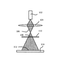
図1には、タイコグラフィー用の機器を概略的に示す。 FIG. 1 schematically shows an apparatus for typography.
図1には、放射線106のビームを形成する放射線源102が示されている。放射線のビームは、プローブ形成手段104により操作(集光)される。対象110には、入力波面108が形成される。対象を貫通した放射線の出力波は、画素化検出器114に伝播し、ここで得られた検出器波面(112)の振幅が検出される。
FIG. 1 shows a
対象の部分の画像を繰り返し取得することにより、各部分が少なくとも一つの他の部分と重なり合い、対象の再構成のため、数学的プロセスに使用され得る画像の組が取得される。 By repeatedly acquiring images of the portion of interest, each portion overlaps at least one other portion, and a set of images is obtained that can be used in a mathematical process for object reconstruction.
異なる用途のため、この概略的な機器は、異なる形態を取っても良いことに留意する必要がある。
例えば、電子顕微鏡の場合、放射線源は、電子源であり(例えば、タングステンフィラメント、ショットキー源またはフィールドエミッタ、および例えば、1keVから300keVの間のエネルギーまで電子を加速する加速手段)、プローブ形成手段は、複数の電子レンズの形態を取っても良く、対象の上のプローブを検出する検出器を有しても良い。
例えば、X線顕微鏡の場合、プローブ形成手段は、フレネルレンズの形態を取っても良く、あるいは単に、ダイアグラム内の開口で形成されても良い。レンズ/開口または対象のいずれかは、例えばピエゾ素子を用いて、機械的に動かされ、対象の異なる部分が照射されても良い。しかしながら、例えば、その後、X線が生成されるアノードに、電子ビームが衝突する衝突位置を変化させることにより、プローブ形成手段に対して、X線源を移動することも可能である。
It should be noted that for different applications, this schematic device may take different forms.
For example, in the case of an electron microscope, the radiation source is an electron source (eg, a tungsten filament, a Schottky source or field emitter, and an accelerating means that accelerates electrons to an energy between 1 keV and 300 keV, for example), and a probe forming means May take the form of a plurality of electron lenses and may have a detector for detecting a probe on the object.
For example, in the case of an X-ray microscope, the probe forming means may take the form of a Fresnel lens, or simply formed with an opening in the diagram. Either the lens / aperture or the object may be mechanically moved, for example using a piezo element, so that different parts of the object are illuminated. However, for example, the X-ray source can be moved with respect to the probe forming means by changing the collision position where the electron beam collides with the anode where X-rays are generated.
この例では、回折面は、無限大であることに留意する必要がある。これは、「かけ離れており」、従って、対象から十分に大きな距離であり、検出器で形成される画像は、ほぼ回折パターンとなる。問題は、画像の直径が大きいことである。対象と検出器の間にレンズを追加することにより、回折面がより好適に配置されるようになる。 It should be noted that in this example, the diffractive surface is infinite. This is “away” and is therefore a sufficiently large distance from the object, and the image formed by the detector will be approximately a diffraction pattern. The problem is that the diameter of the image is large. By adding a lens between the object and the detector, the diffractive surface is more suitably arranged.
図2Aには、タイコグラフィックイメージングの従来のフローチャートを概略的に示す。 FIG. 2A schematically shows a conventional flowchart of typographic imaging.
図2Aには、数学的再構成において行われるステップが示されている。 FIG. 2A shows the steps performed in the mathematical reconstruction.
ステップ200では、多くの(重複する)画像が取得され、対象、入力波、および伝播関数の数学的予測が行われる。対象の数学的予測は、極めて大まかな予測であっても良く、例えば「空の」対象(全てのノードが一つに設定される)であっても良い。
ゼロのみを有する空の対象から開始すると、うまく動作しないことに留意する必要がある。
また、入力波は、例えば、トップヘッド近似に簡略化され得る。この場合、画像は、回折面において検出され、伝播関数は、フーリエ変換である。
In
Note that starting from an empty object with only zero does not work well.
Also, the input wave can be simplified to top head approximation, for example. In this case, the image is detected at the diffractive surface and the propagation function is a Fourier transform.
ステップ202では、出口波、すなわち、対象を貫通した入力波が計算される。出力波は、入力波と対象の透過関数の単純なかけ算で計算されると仮定される。
In
ステップ204では、出力波が検出器面に伝播される。
In
ステップ206では、各画素において、前記画素に関連するノードに、測定強度の平方根が割り当てられる。
In
ステップ210では、改変された値を有するこれらのノードは、対物面に向かって逆向きに伝播する。
In
ステップ212では、対象の(複素)表示が更新される。必要な場合、入力波(プローブ)も更新される。
In
ステップ214では、中断基準を用いて、反復が完了される。中断基準は、反復の数であっても良く、あるいは連続する反復の間の変化に基づいても良い。基準に合致すると、再構成された対象が結果となり、そうでなければ、さらなる反復が行われる。
In
反復の完了後に、再構成された対象が現れるが、これは、良好な表示であるとは限られないことに留意する必要がある。あまりに多くの反復により反復が完了した場合、この方法は、収束されない可能性がある。また、連続する反復の間の変化が小さい場合、これは、表示が良好な表示であることを意味しない。 It should be noted that after the iteration is complete, the reconstructed object appears, but this is not always a good display. If the iterations are completed with too many iterations, this method may not converge. Also, if the change between successive iterations is small, this does not mean that the display is a good display.
図2Bには、本発明によるタイコグラフィックイメージングのフローチャートを概略的に示す。 FIG. 2B schematically shows a flow chart of typographic imaging according to the present invention.
図に示すように、ステップ208を除き、全てのステップは、図2Aに示した従来の方法と等しい。測定値をノードに割り当てる代わりに、各画素用に、その画素に対応する全てのノードの強度が、それらの合計(積分)値が測定値と整合するまで、相互にスケール化される。これにより、対物面の視野は、入力波全体を収容できるほど、十分に大きく維持される。これは、入力波の部分が視野からはみ出るような、図2Aに示した方法とは異なる。これにより、本発明は、あまりに少ない検出器画素を使用した際の問題に対処できる。画素は、検出器面において、大きく維持され、被照射検出器面領域全体が収集できる。
As shown in the figure, except for
図3には、セグメント化された検出器を概略的に示す。 FIG. 3 schematically shows a segmented detector.
図3には、対物面から見たセグメント化された検出器が示されている。半径300と302の間の面は、4つの四分円302A、302B、302C、302Dに分割される。これらの四分円の各々は、検出器の画素となる。同様に、半径300内の領域は、4つの四分円に分割され、各四分円は、画素となる。従って、得られる検出器は、合計8個の画素を有する。
FIG. 3 shows a segmented detector as viewed from the object plane. The plane between the
内側部分を形成する画素は、それらを取り囲む画素と同一の表面積を有しても良い。あるいは、これらは、異なる表面積を有しても良い。他のセグメント化された検出器は、各半径組の間に、5以上の四分円を有しても良く、および/またはより多くの半径の間に、より多くの画素を定めても良い。しかしながら、後に示すように、比較的少ない画素数において、本願発明者らは、高品質の対象の再構成を達成している。 The pixels forming the inner part may have the same surface area as the pixels surrounding them. Alternatively, they may have different surface areas. Other segmented detectors may have 5 or more quadrants between each radius set and / or define more pixels between more radii. . However, as will be shown later, the inventors have achieved high quality object reconstruction with a relatively small number of pixels.
このタイプの検出器は、明視野/暗視野(BFDF)検出器として、電子顕微鏡において既に使用されていることに留意する必要がある。通常、内側の画素(明視野)は、未散乱ビームの検出に使用され、外側画素(暗視野)は、散乱電子に使用される。しかしながら、例えば8×8グリッドに配置された、四角い限られた量の画素を有する検出器を使用することも可能である。 It should be noted that this type of detector is already used in electron microscopes as a bright field / dark field (BFDF) detector. Typically, the inner pixel (bright field) is used for detection of unscattered beams and the outer pixel (dark field) is used for scattered electrons. However, it is also possible to use a detector with a limited amount of square pixels, for example arranged in an 8 × 8 grid.
図4A乃至4Cには、透過型電子顕微鏡を使用し、異なる数の画素を用いた、同じ対象の従来の再構成画像を示す(薄い対象のモジュラスは、常に1であるため、位相を示す)。(シミュレーションされた)対象は、アモルファスカーボンの実際の薄い層を表す。高強度スパイクは、炭素原子を表す。データ組を生成するために使用されるプローブは、球面収差が2.7mmmで、開口角が7mradで、シェルツァー(Scherzer)条件からのデフォーカスが50nmの、(シミュレーションされた)実際のプローブである。これは、当業者には良く知られている。 FIGS. 4A-4C show a conventional reconstructed image of the same object using a transmission electron microscope and using a different number of pixels (the modulus of the thin object is always 1, indicating phase) . The object (simulated) represents an actual thin layer of amorphous carbon. High intensity spikes represent carbon atoms. The probe used to generate the data set is a real (simulated) probe with a spherical aberration of 2.7 mm, an aperture angle of 7 mrad, and a defocus from Scherzer conditions of 50 nm. . This is well known to those skilled in the art.
画像は、仮想検出器により測定された、シミュレーションされたデータ組を用いて取得される。ダイナミックレンジに対するいかなる制限もなされない。各画像における検出器のサイズは、一定に維持され、従って、同様の最大散乱角が収集される。しかしながら、仮想検出器は、画素の数および画素サイズが異なり、データはビニングされ(検出器のいくつかの素子のデータが、一つの画素にまとめられる)、図4Aでは、画素の数は、512×512であり、図4Bでは、画素の数は、256×256であり(2×2のビニング)、図4Cでは、画素の数は、128×128(4×4のビニング)である。これは、検出器面でのノードの数が異なること、さらには散乱角を定める角度分解能が異なることを意味する。対象の数学的予測のノードが、検出器画素と1対1の関係を有すると、逆変換の後に再構成される対象の視野は、512×512画素の使用のときに最高となり、128×128画素の使用のとき最低となる。再構成対象は、画素の数が減ると「拡大」される。 The image is acquired using a simulated data set measured by a virtual detector. There are no restrictions on the dynamic range. The size of the detector in each image is kept constant, so a similar maximum scattering angle is collected. However, the virtual detector is different in the number of pixels and the pixel size, the data is binned (data of several elements of the detector are combined into one pixel), and in FIG. 4A, the number of pixels is 512 In FIG. 4B, the number of pixels is 256 × 256 (2 × 2 binning), and in FIG. 4C, the number of pixels is 128 × 128 (4 × 4 binning). This means that the number of nodes on the detector surface is different, and further the angular resolution that determines the scattering angle is different. If the mathematical prediction node of the object has a one-to-one relationship with the detector pixels, the field of view of the object reconstructed after the inverse transform is highest when using 512 × 512 pixels, and 128 × 128 Minimum when using pixels. The reconstruction target is “enlarged” as the number of pixels decreases.
図4Aにおいて使用される仮想検出器は、512×512画素を有する。再構成対象(の位相)は、大きな数のドットを示す。 The virtual detector used in FIG. 4A has 512 × 512 pixels. The reconstruction target (phase) indicates a large number of dots.
図4Bには、図4Aにおいて使用された同一のシミュレーションデータ組が、2×2でビニングされた際の結果を示す。256×256画素の仮想検出器が得られる。再構成対象(の位相)は、もはやドットを示さず、多くの同一構造は、「エアプレイン」と称される。これは、アーチファクトを表す。注意深い解析により、「エアプレイン」の位置は、図4Aのドットの位置と似通っていることが示されるが、2倍に拡大されている。 FIG. 4B shows the result when the same simulation data set used in FIG. 4A is binned by 2 × 2. A virtual detector of 256 × 256 pixels is obtained. The object to be reconstructed no longer shows dots and many identical structures are referred to as “airplanes”. This represents an artifact. Careful analysis shows that the location of the “airplane” is similar to the dot location in FIG. 4A, but has been magnified by a factor of two.
図4Cでは、同じデータ組が使用されるが、ビニングは4×4であり、128×128画素の仮想検出器が得られる。対象(の位相)の再構成は、完全に失敗に終わる。 In FIG. 4C, the same data set is used, but the binning is 4 × 4 and a virtual detector of 128 × 128 pixels is obtained. The reconstruction of the object phase completely fails.
図5A乃至5Cには、従来の方法を用いて得られた、再構成(または既知の予想)プローブの強度を示す。再構成プローブは、仮想検出器により測定された、シミュレーションデータ組を用いて取得される。ダイナミックレンジに対して、いかなる制限もされていない。画像の各々における検出器のサイズは、同位置に維持され、従って、同じ最大散乱角が捕獲される。しかしながら、仮想検出器は、画素の数および画素サイズが異なり、データがビニングされ(検出器のいくつかの素子のデータは、一つの画素に統合される)、図5Aでは、画素の数は、512×512であり(ビニング1×1)、図5Bでは、画素の数は、256×256であり(ビニング2×2)、図5Cでは、画素の数は、128×128である(ビニング4×4)。これは、検出器面におけるノードの数、さらには散乱角を定める角度分解能が、異なることを意味する。プローブの数学的予測のノードは、検出器画素と1対1の関係を有し、逆変換の後に再構成されるプローブの視野は、512×512画素を使用したとき最大となり、128×128画素を使用したとき最小となる。再構成対象の場合、再構成プローブは、画素の数が低下すると、「拡大」される。 Figures 5A-5C show the strength of the reconstructed (or known predicted) probe obtained using conventional methods. The reconstructed probe is acquired using a simulation data set measured by a virtual detector. There are no restrictions on the dynamic range. The size of the detector in each of the images is kept in the same position, so the same maximum scattering angle is captured. However, the virtual detector is different in the number of pixels and the pixel size, and the data is binned (data of several elements of the detector are combined into one pixel). In FIG. 5A, the number of pixels is 512 × 512 (binning 1 × 1), in FIG. 5B, the number of pixels is 256 × 256 (binning 2 × 2), and in FIG. 5C, the number of pixels is 128 × 128 (binning 4 × 4). This means that the number of nodes on the detector plane, as well as the angular resolution that determines the scattering angle, are different. The probe's mathematical prediction node has a one-to-one relationship with the detector pixels, and the field of view of the probe reconstructed after the inverse transform is maximum when using 512x512 pixels, and 128x128 pixels Minimum when using. In the case of a reconstruction target, the reconstruction probe is “enlarged” as the number of pixels decreases.
図5Aには、エアリーディスク(プローブの振幅)を示す。これは、視野の外部でほとんど強度を有さない。 FIG. 5A shows an Airy disk (probe amplitude). This has little intensity outside the field of view.
図5Bには、エアリーディスク(プローブの振幅)を示す。これは、視野の外部で、小さな強度を有し、これは、エイリアシングにより畳まれる(fold)。 FIG. 5B shows an Airy disk (probe amplitude). This has a small intensity outside the field of view, which is folded by aliasing.
図5Cには、エアリーディスク(プローブの振幅)を示す。これは、視野の外側で大きな強度を有し、これは、エイリアシングにより畳まれれ、プローブの大きく歪んだ表示が得られる。 FIG. 5C shows an Airy disk (probe amplitude). This has a large intensity outside the field of view, which is folded by aliasing, resulting in a highly distorted display of the probe.
図4A乃至4Cおよび図5A乃至5Cには、従来の方法では、照射全体を収容できる(プローブを完全に含む)、十分に大きな対物面における視野が得られるような画素サイズおよび多くの画素を有する検出器が必要になること、一方、フーリエ空間(検出器面)では、これは、データを完全に網羅することが示されている。これは、再構成されたプローブを観測する際に、最も良く認められる。図5Bに示されている僅かなはみ出しでも、図4Bに示すようなアーチファクトが得られる結果となる。 4A-4C and FIGS. 5A-5C have a pixel size and many pixels that can accommodate the entire illumination (completely including the probe) and provide a sufficiently large field of view in the object plane in the conventional method. It has been shown that in the Fourier space (detector plane) this requires complete coverage of the data while a detector is required. This is best seen when observing the reconstructed probe. Even a slight protrusion shown in FIG. 5B results in an artifact as shown in FIG. 4B.
図6A乃至6Cには、本発明を用いた対象の再構成の結果を示す。前述の場合と同じ(シミュレーション)対象および(シミュレーションされた)プローブ条件が使用されている。 6A to 6C show the results of object reconstruction using the present invention. The same (simulated) object and (simulated) probe conditions are used as before.
使用された方法では、対物面および検出器面におけるノードの数は、検出器の画素の数とは無関係に、一定に維持される。ノードの数は、512×512であり、図6Aにおける画素の数は、512×512(ビニングなし)であり、図6Bにおける画素の数は、128×128(ビニング4×4)であり、図6Cにおける画素の数は、32×32(ビニング16×16)である。ノードの数を一定に維持することにより、対象の全ての再構成画像が、画素の数によらず、同じ拡大倍率を示す。 In the method used, the number of nodes in the object plane and detector plane is kept constant regardless of the number of pixels in the detector. The number of nodes is 512 × 512, the number of pixels in FIG. 6A is 512 × 512 (no binning), and the number of pixels in FIG. 6B is 128 × 128 (binning 4 × 4), The number of pixels in 6C is 32 × 32 (binning 16 × 16). By keeping the number of nodes constant, all the reconstructed images of interest show the same magnification, regardless of the number of pixels.
使用される画素の数が同一なので、図6Aに示す再構成された対象(の位相)は、図4Aにおける再構成された対象(の位相)と比較可能である。薄いサンプルに関して、位相のみが示されており、振幅は一つであることに留意する必要がある。 Since the number of pixels used is the same, the reconstructed object shown in FIG. 6A can be compared to the reconstructed object in FIG. 4A. Note that for thin samples, only the phase is shown and the amplitude is one.
図4Cに示した失敗した再構成の場合と同じ数の画素を用いた、図6Bに示す再構成された対象(の位相)は、依然として、優れた結果を示している。再構成される対象の面積は、図6Aの場合よりも小さいことに留意する必要がある。 The reconstructed object shown in FIG. 6B with the same number of pixels as in the failed reconstruction shown in FIG. 4C still shows excellent results. It should be noted that the area to be reconstructed is smaller than in the case of FIG. 6A.
また、32×32画素のみを用いた、図6Cに示す再構成された対象(の位相)は、対象の再構成部分がさらに制限されるにも関わらず、優れた結果を示す。(従来の再構成に必要な画素数に比べて)このような極めて少ない数でも、高品質の再構成が得られる。 In addition, the reconstructed target (phase) shown in FIG. 6C using only 32 × 32 pixels shows excellent results even though the reconstructed part of the target is further limited. Even with such a very small number (compared to the number of pixels required for conventional reconstruction), a high quality reconstruction is obtained.
少ない画素数が、必ずしも計算数が減ることを意味しないことに留意する必要がある。少ない画素数を使用すると、同様の結果を得るのに、より多くの画像が必要となる。 It should be noted that a small number of pixels does not necessarily mean a reduction in the number of calculations. Using a smaller number of pixels requires more images to achieve a similar result.
図7A乃至7Cには、検出器面/画素における、再構成された振幅(強度の平方根)を示す。ここでも、対物面および検出器面におけるノードの数は、検出器の画素数には依存せず、一定である。 7A-7C show the reconstructed amplitude (square root of intensity) at the detector plane / pixel. Again, the number of nodes on the object plane and detector plane is constant, independent of the number of pixels in the detector.
(合計)明視野強度は、合計暗視野強度よりも数桁大きいため、全ての検出器データの再構成において、平均明視野の寄与は差し引かれていることに留意する必要がある。これは、薄い対象である対象の直接の結果である。この減算の結果、中央領域は、より暗く見えるが、この領域には、小さな変化が明らかに示されている。また、これは、本方法を基本的に制限するものではなく、より良い例示のみのため行われることに留意する必要がある。 It should be noted that since the (total) bright field intensity is several orders of magnitude greater than the total dark field intensity, the average bright field contribution has been subtracted in all detector data reconstructions. This is a direct result of a thin object. As a result of this subtraction, the central area appears darker, but small changes are clearly shown in this area. It should also be noted that this is not a fundamental limitation of the method and is done for better illustration only.
振幅(amplitude)は、パターンを視認することを可能にするために使用される。そうでなければ、明視野ディスクの外側の強度(これは清算された振幅である)は、極めて低く、明視野ディスク強度を減算した後も、何も視認することはできない。 Amplitude is used to allow the pattern to be viewed. Otherwise, the intensity outside the bright field disc (which is the settled amplitude) is very low and nothing can be seen after subtracting the bright field disc intensity.
ノードの数は、512×512であり、図7Aにおける画素の数は、512×512(ビニングなし)であり、図7Bにおける画素の数は、128×128(ビニング4×4)であり、図7Cにおける画素の数は、32×32(ビニング16×16)である。ノードの数は一定に維持され、対象の全ての再構成画像は、画素数に関わらず、同じ拡大倍率を示す。 The number of nodes is 512 × 512, the number of pixels in FIG. 7A is 512 × 512 (no binning), and the number of pixels in FIG. 7B is 128 × 128 (binning 4 × 4), The number of pixels in 7C is 32 × 32 (binning 16 × 16). The number of nodes is kept constant, and all the reconstructed images of interest show the same magnification regardless of the number of pixels.
図7A乃至7Cには、各画素において、前記画素を構成するノードの合計を示す。 7A to 7C show the total number of nodes constituting each pixel in each pixel.
図7Aでは、ノードの数および画素の数が等しいため、合計は不要である。ここでは、各画素と各ノードの間に、1対1の関係が存在する。 In FIG. 7A, the total is not necessary because the number of nodes and the number of pixels are equal. Here, a one-to-one relationship exists between each pixel and each node.
図7Bでは、各画素は、16のノード(ビニング4×4)に対応し、図には、画素の強度(前記画素に対応する16のノード全ての合計)が示されている。 In FIG. 7B, each pixel corresponds to 16 nodes (binning 4 × 4), and the figure shows the intensity of the pixel (the sum of all 16 nodes corresponding to the pixel).
図7Bでは、各画素は、256個のノード(ビニング16×16)に対応し、図には、画素の強度(前記画素に対応する256のノード全ての合計)が示されている。 In FIG. 7B, each pixel corresponds to 256 nodes (binning 16 × 16), and the pixel intensity (the sum of all 256 nodes corresponding to the pixel) is shown in the figure.
図から分かるように、検出される強度の印象は、再構成の粒状態(画素の数に依存する)は異なるものの、相互に似通っている。再構成された検出器データと検出器データの比較では、高い同一性が示されていることに留意する必要がある。 As can be seen from the figure, the impressions of detected intensity are similar to each other, although the grain state of the reconstruction (depending on the number of pixels) is different. It should be noted that the comparison between the reconstructed detector data and the detector data shows high identity.
図8Aには、512×512ノードとして表された、オリジナルの対象データ(の位相)(シミュレーションデータ)の組を示す。前述の場合と同じ(シミュレーション)対象と(シミュレーション)プローブ条件が使用されている。これにより、512×512ノードの振幅を示す、図8Bに示す検出器データ組が得られる。ノードが複素数のため、シミュレーション入力データは、位相を表すことができる。(検出器面における)位相は、図8Cに示されている。これらは、全てシミュレーション入力データであり、図8Bのデータを用いて、これに近い再構成を取得することが期待される。通常、これは、512×512画素の検出器によってのみ、可能となる。しかしながら、この場合、16のセグメント検出器(別途図10に示されている)が使用される。図8Dには、シミュレーション入力データを用いた振幅(この16のセグメント検出器により「測定された」信号の平方根)が示されている。 FIG. 8A shows a set of original target data (phase thereof) (simulation data) represented as 512 × 512 nodes. The same (simulation) object and (simulation) probe conditions are used as in the previous case. This results in the detector data set shown in FIG. 8B showing the amplitude of 512 × 512 nodes. Since the nodes are complex numbers, the simulation input data can represent the phase. The phase (at the detector plane) is shown in FIG. 8C. These are all simulation input data, and it is expected that a reconstruction close to this will be obtained using the data of FIG. 8B. Usually this is only possible with a 512 × 512 pixel detector. However, in this case, 16 segment detectors (separately shown in FIG. 10) are used. FIG. 8D shows the amplitude using the simulation input data (the square root of the signal “measured” by the 16 segment detector).
図9Aには、第1の面(対物面)および第2の面(検出器面)の計算のため、16のセグメント検出器および512×512ノードを用いて再構成された対象(の位相)を示す。図9Bには、検出器面における再構成された512×512ノードを示す。図9Cには、再構成された位相情報(しばしば偽色で表示される)を示し、図9Dには、検出器のセグメントに対応するノードの合計の振幅を示す。 Figure 9A shows the phase reconstructed using 16 segment detectors and 512 x 512 nodes for the calculation of the first (objective) and second (detector) planes. Indicates. FIG. 9B shows a reconstructed 512 × 512 node in the detector plane. FIG. 9C shows the reconstructed phase information (often displayed in false color), and FIG. 9D shows the total amplitude of the nodes corresponding to the detector segments.
図から分かるように、再構成された対象の(位相の)鮮明さは、オリジナルに比べて僅かに劣るが、(ほとんど)全ての特徴が識別できる。また、再構成された領域(検出器領域)において、振幅および位相は、オリジナルデータと極めて似通っている。これは、比較的単純な検出器(僅か16のセグメント)を用いて、対象を高品質の表現で再構成することが可能であることを示唆する。16のエレメントの検出器の読み取り速度が、512×512画素の検出器に比べて、十分に速いことは、良く知られている。また、セグメントの領域がより大きくなるため、検出された信号は、低い信号対ノイズを示し、出力信号のダイナミックレンジは低くなり、これにより、検出器に対する要望が緩和される。 As can be seen, the (phase) sharpness of the reconstructed object is slightly inferior to the original, but (almost) all features can be identified. In the reconstructed area (detector area), the amplitude and phase are very similar to the original data. This suggests that the object can be reconstructed with a high quality representation using a relatively simple detector (only 16 segments). It is well known that the 16 element detector reading speed is sufficiently faster than a 512 × 512 pixel detector. Also, because the segment area is larger, the detected signal exhibits low signal-to-noise and the dynamic range of the output signal is reduced, thereby alleviating the desire for the detector.
図10には、図8A乃至8D、および図9A乃至9Dのシミュレーションに使用された16セグメント検出器を示す。検出器は、12のセグメント5乃至16のリングで取り囲まれた、4つの内部四分円1乃至4で構成される。検出器は、フォトダイオード技術を用いたシリコン装置、またはStoyanの米国特許US8426831B2に記載のボロン層を用いた、より複雑なシリコン装置であることが好ましい。ただし、検出器をベースとしたシンチレータも想定される。
FIG. 10 shows a 16-segment detector used in the simulations of FIGS. 8A to 8D and FIGS. 9A to 9D. The detector consists of four
まとめると、画素の数が極めて少ないとき、従来のタイコグラフィーを実施する際に問題が生じる。通常、対象の高品質の再構成を得るには、(ビニングの後)多くの画素が必要となる。本願発明者らは、検出器の画素数よりも多くのノード(例えば512×512ノード)を有する計算面を使用することにより、例えば、16セグメント検出器または32×32画素の検出器を使用した場合であっても、対象の高品質の再構成が行えることを見出した。より大きな画素サイズのため、多くのフラックスが遮蔽され、検出器の、例えば、検出器S/N比およびダイナミックレンジに対する要望が軽減される。 In summary, when the number of pixels is very small, problems arise when performing conventional typography. Usually, many pixels are needed (after binning) to obtain a high quality reconstruction of the object. The inventors have used, for example, a 16 segment detector or a 32 × 32 pixel detector by using a computational plane with more nodes (eg 512 × 512 nodes) than the number of pixels of the detector. Even in this case, it was found that the target can be reconstructed with high quality. Because of the larger pixel size, more flux is shielded, reducing the detector's desire for, for example, detector S / N ratio and dynamic range.
102 放射線源
104 プローブ形成手段
106 放射線
108 入力波面
110 対象
112 検出器波面
114 画素化検出器
102 Radiation source
104 Probe formation means
106 Radiation
108 Input wavefront
110 target
112 Detector wavefront
114 pixelated detector
Claims (20)
対物面に対象を提供するステップと、
検出器面に画素化検出器を提供するステップであって、前記検出器面は、フレネル伝播関数により前記対物面と共役化(conjugated)され、前記画素化検出器は、波面の強度を検出するように構成される、ステップと、
放射線源、および前記対物面に入力波面を形成するように構成されたプローブ形成手段を提供するステップであって、前記入力波面は、前記対象により出力波面に変換される、ステップと、
前記対象の第1の数学的予測、前記フレネル伝播関数の予測、および前記入力波面の予測を提供するステップであって、前記対象の前記数学的予測は、第1の計算面における複数のノードによって表され、各ノードは、複素数である、ステップと、
以下のステップ:
前記対象の照射される領域を選択するステップ、
前記領域に放射線を照射するステップ、
前記画素化検出器における検出器波面の強度を検出して、検出器画像を得るステップ、
各照射された領域を、少なくとも一つの他の照射された領域と重ね合わせるステップ、
により、少なくとも2つの画像を取得するステップと、
前記第1の計算面において、前記対象の前記数学的予測を前記入力波面の前記予測と掛け合わせた後、および第2の計算面の複数のノードにより表される前記画像の数学的予測に対する、前記フレネル伝播関数を用いた伝播処理の後、前記検出器画像の画素の検出された強度を、前記少なくとも2つの画像において、前記第2の計算面における前記画像の前記数学的予測の対応する領域の強度に整合させることで、前記対象の前記数学的予測を更新するステップを、中断基準に合致するまで反復するステップと、
を有し、
前記検出器画像の画素は、前記第2の計算面の2以上のノードに対応し、
前記更新するステップの間、各画素の測定強度は、前記画素に対応する全てのノードの強度の合計に整合されることを特徴とする方法。 A method of typographic imaging,
Providing an object on the object plane;
Providing a pixelated detector at a detector plane, wherein the detector plane is conjugated with the object plane by a Fresnel propagation function, the pixelated detector detecting a wavefront intensity; Configured as steps, and
Providing a radiation source and probe forming means configured to form an input wavefront at the object plane, wherein the input wavefront is converted to an output wavefront by the object; and
Providing a first mathematical prediction of the object, a prediction of the Fresnel propagation function, and a prediction of the input wavefront, wherein the mathematical prediction of the object is determined by a plurality of nodes in a first calculation surface. Each node is a complex number, steps,
The following steps:
Selecting an illuminated area of the object;
Irradiating the region with radiation;
Detecting a detector wavefront intensity in the pixelated detector to obtain a detector image;
Superimposing each irradiated region with at least one other irradiated region;
Obtaining at least two images,
In the first calculation plane, after multiplying the mathematical prediction of the object with the prediction of the input wavefront , and for a mathematical prediction of the image represented by a plurality of nodes of a second calculation plane, After the propagation process using the Fresnel propagation function, the detected intensity of the pixels of the detector image is the corresponding region of the mathematical prediction of the image in the second calculation plane in the at least two images. Repeating the step of updating the mathematical prediction of the object by matching to the intensity of
Have
The pixels of the detector image correspond to two or more nodes of the second calculation surface,
During the updating step, the measured intensity of each pixel is matched to the sum of the intensities of all nodes corresponding to the pixel .
前記フレネル伝播関数は、フーリエ変換である、請求項1に記載の方法。 The detector surface is a diffractive surface, or a surface conjugated to it,
The method of claim 1, wherein the Fresnel propagation function is a Fourier transform.
前記整数は、1よりも大きい、請求項1に記載の方法。 Each pixel of the pixelated detector corresponds to an integer number of nodes in the second calculation plane,
The method of claim 1, wherein the integer is greater than one.
前記画素に関連する前記第2の計算面における対応するノードは、前記反復するステップの間、更新されない、請求項1に記載の方法。 Signals of at least one pixel of the pixelated detector, in the step of the iteration, is ignored,
The corresponding node in the second computing surface, during said repetition, not updated, the method according to claim 1 associated with the pixel.
前記光放射線は、赤外線、可視光、紫外線、およびX線を有し、前記粒子放射線は、電子、中性子、原子、およびイオンを有する、請求項1に記載の方法。 The radiation is radiation from a group of light radiation or particle radiation;
2. The method of claim 1, wherein the optical radiation comprises infrared, visible light, ultraviolet, and X-rays, and the particle radiation comprises electrons, neutrons, atoms, and ions.
前記対象の前記数学的予測、前記フレネル伝播関数の予測、および前記入力波面の予測を用いて、前記第2の計算面のノードに対する複素数を計算するステップと、
前記画素化検出器の各画素のため、各画素に関連する前記第2の計算面の前記ノードで、前記複素数をスケール化し、前記第2の計算面において、前記検出器画像の画素の検出強度を、前記画像の前記得られた数学的予測の前記対応するノードの積分強度に整合させるステップと、
前記画像の前記得られた数学的予測を、前記対物面に戻るように伝播させるステップと、
前記対象の前記数学的予測を更新するステップと、
を有する、請求項1に記載の方法。 Updating the mathematical prediction of the object comprises:
Using the mathematical prediction of the object, the prediction of the Fresnel propagation function, and the prediction of the input wavefront to calculate a complex number for a node of the second calculation surface;
For each pixel of the pixelated detector, the complex number is scaled at the node of the second calculation plane associated with each pixel, and the detection intensity of the pixel of the detector image in the second calculation plane Matching the integrated intensity of the corresponding node of the obtained mathematical prediction of the image;
Propagating the obtained mathematical prediction of the image back to the object plane;
Updating the mathematical prediction of the object ;
The method of claim 1, comprising:
制御器と、
を備える機器であって、
前記制御器は、請求項1に記載の方法を実行するようにプログラム化される、機器。 A pixelated detector that is sensitive to the radiation generated by the radiation source;
A controller;
A device comprising:
The apparatus, wherein the controller is programmed to perform the method of claim 1.
前記プローブ形成手段は、電子光学レンズおよび偏向器を有し、
前記画素化検出器は、画素化電子検出器である、請求項9に記載の機器。 The radiation source is an electron source;
The probe forming means has an electro-optic lens and a deflector,
10. The apparatus of claim 9, wherein the pixelated detector is a pixelated electron detector.
前記プローブ形成手段は、開口を示すダイアフラムを有し、
前記画素化検出器は、画素化X線検出器である、請求項9に記載の機器。 The radiation source is an X-ray source;
The probe forming means has a diaphragm showing an opening,
10. The apparatus of claim 9, wherein the pixelated detector is a pixelated X-ray detector.
前記プローブ形成手段は、近接場走査型光顕微鏡プローブを有し、
前記画素化検出器は、画素化光検出器である、請求項9に記載の機器。 The radiation source is a light source;
The probe forming means has a near-field scanning optical microscope probe,
10. The apparatus of claim 9, wherein the pixelated detector is a pixelated photodetector.
前記フレネル伝播関数は、フーリエ変換である、請求項2に記載の方法。 The detector surface is a diffractive surface, or a surface conjugated to it,
The method of claim 2, wherein the Fresnel propagation function is a Fourier transform.
前記整数は、1よりも大きい、請求項2に記載の方法。 Each pixel of the pixelated detector corresponds to an integer number of nodes in the second calculation plane,
The method of claim 2, wherein the integer is greater than one.
前記画素に関連する前記第2の計算面における対応するノードは、前記反復するステップの間、更新されない、請求項2に記載の方法。 Signals of at least one pixel of the pixelated detector, in the step of the iteration, is ignored,
The corresponding node in the second computing surface, during said repetition, not updated, the method according to claim 2 associated with the pixel.
前記光放射線は、赤外線、可視光、紫外線、およびX線を有し、前記粒子放射線は、電子、中性子、原子、およびイオンを有する、請求項2に記載の方法。 The radiation is radiation from a group of light radiation or particle radiation;
3. The method of claim 2, wherein the optical radiation comprises infrared, visible light, ultraviolet, and X-rays, and the particle radiation comprises electrons, neutrons, atoms, and ions.
前記対象の前記数学的予測、前記フレネル伝播関数の予測、および前記入力波面の予測を用いて、前記第2の計算面のノードに対する複素数を計算するステップと、
前記画素化検出器の各画素のため、各画素に関連する前記第2の計算面の前記ノードで、前記複素数をスケール化し、前記第2の計算面において、前記検出器画像の画素の検出強度を、前記画像の前記得られた数学的予測の前記対応するノードの積分強度に整合させるステップと、
前記画像の前記得られた数学的予測を、前記対物面に戻るように伝播させるステップと、
前記対象の前記数学的予測を更新するステップと、
を有する、請求項2に記載の方法。 Updating the mathematical prediction of the object comprises:
Using the mathematical prediction of the object, the prediction of the Fresnel propagation function, and the prediction of the input wavefront to calculate a complex number for a node of the second calculation surface;
For each pixel of the pixelated detector, the complex number is scaled at the node of the second calculation plane associated with each pixel, and the detection intensity of the pixel of the detector image in the second calculation plane Matching the integrated intensity of the corresponding node of the obtained mathematical prediction of the image;
Propagating the obtained mathematical prediction of the image back to the object plane;
Updating the mathematical prediction of the object ;
The method of claim 2, comprising:
Applications Claiming Priority (2)
| Application Number | Priority Date | Filing Date | Title |
|---|---|---|---|
| EP15172752.6A EP3106862B1 (en) | 2015-06-18 | 2015-06-18 | Method of ptychographic imaging |
| EP15172752.6 | 2015-06-18 |
Publications (3)
| Publication Number | Publication Date |
|---|---|
| JP2017009603A JP2017009603A (en) | 2017-01-12 |
| JP2017009603A5 JP2017009603A5 (en) | 2018-07-05 |
| JP6416825B2 true JP6416825B2 (en) | 2018-10-31 |
Family
ID=53489830
Family Applications (1)
| Application Number | Title | Priority Date | Filing Date |
|---|---|---|---|
| JP2016117624A Active JP6416825B2 (en) | 2015-06-18 | 2016-06-14 | Tyco graphic imaging method |
Country Status (4)
| Country | Link |
|---|---|
| US (1) | US9959639B2 (en) |
| EP (1) | EP3106862B1 (en) |
| JP (1) | JP6416825B2 (en) |
| CN (1) | CN106257323B (en) |
Families Citing this family (4)
| Publication number | Priority date | Publication date | Assignee | Title |
|---|---|---|---|---|
| CN107796837B (en) * | 2017-10-09 | 2019-10-29 | 南京大学 | A kind of imaging device, imaging method and imaging system |
| US10755892B2 (en) * | 2018-05-23 | 2020-08-25 | Kla-Tencor Corporation | Reflection-mode electron-beam inspection using ptychographic imaging |
| AU2019403134A1 (en) * | 2018-12-18 | 2021-06-17 | Pathware Inc. | Computational microscopy based-system and method for automated imaging and analysis of pathology specimens |
| CN110411983B (en) * | 2019-07-26 | 2022-05-27 | 南方科技大学 | High-resolution diffraction imaging method and device |
Family Cites Families (15)
| Publication number | Priority date | Publication date | Assignee | Title |
|---|---|---|---|---|
| GB0409572D0 (en) * | 2004-04-29 | 2004-06-02 | Univ Sheffield | High resolution imaging |
| US8138485B2 (en) | 2007-06-25 | 2012-03-20 | Asml Netherlands B.V. | Radiation detector, method of manufacturing a radiation detector, and lithographic apparatus comprising a radiation detector |
| JP5764380B2 (en) | 2010-04-29 | 2015-08-19 | エフ イー アイ カンパニFei Company | SEM imaging method |
| GB201016088D0 (en) * | 2010-09-24 | 2010-11-10 | Phase Focus Ltd | Improvements in imaging |
| GB201020516D0 (en) * | 2010-12-03 | 2011-01-19 | Univ Sheffield | Improvements in providing image data |
| GB201107053D0 (en) * | 2011-04-27 | 2011-06-08 | Univ Sheffield | Improvements in providing image data |
| GB201112119D0 (en) * | 2011-07-14 | 2011-08-31 | Univ Sheffield | Method and apparatus for position determination |
| US8704176B2 (en) | 2011-08-10 | 2014-04-22 | Fei Company | Charged particle microscope providing depth-resolved imagery |
| EP2690648B1 (en) | 2012-07-26 | 2014-10-15 | Fei Company | Method of preparing and imaging a lamella in a particle-optical apparatus |
| GB201215558D0 (en) * | 2012-08-31 | 2012-10-17 | Phase Focus Ltd | Improvements in phase retrieval |
| US9864184B2 (en) * | 2012-10-30 | 2018-01-09 | California Institute Of Technology | Embedded pupil function recovery for fourier ptychographic imaging devices |
| AU2013338193A1 (en) * | 2012-10-30 | 2015-05-21 | California Institute Of Technology | Fourier ptychographic imaging systems, devices, and methods |
| EP2879156A1 (en) | 2013-12-02 | 2015-06-03 | Fei Company | Charged-particle microscopy with enhanced electron detection |
| EP2887381B1 (en) | 2013-12-18 | 2016-09-21 | Fei Company | Method of investigating the wavefront of a charged-particle beam |
| EP2911180A1 (en) | 2014-02-24 | 2015-08-26 | FEI Company | Method of examining a sample in a charged-particle microscope |
-
2015
- 2015-06-18 EP EP15172752.6A patent/EP3106862B1/en active Active
-
2016
- 2016-06-14 JP JP2016117624A patent/JP6416825B2/en active Active
- 2016-06-17 CN CN201610431548.0A patent/CN106257323B/en active Active
- 2016-06-17 US US15/186,267 patent/US9959639B2/en active Active
Also Published As
| Publication number | Publication date |
|---|---|
| CN106257323A (en) | 2016-12-28 |
| US9959639B2 (en) | 2018-05-01 |
| EP3106862B1 (en) | 2019-01-16 |
| EP3106862A1 (en) | 2016-12-21 |
| JP2017009603A (en) | 2017-01-12 |
| CN106257323B (en) | 2019-04-30 |
| US20170024908A1 (en) | 2017-01-26 |
Similar Documents
| Publication | Publication Date | Title |
|---|---|---|
| JP5619767B2 (en) | Supplying image data | |
| EP1740975B1 (en) | High resolution imaging | |
| JP6416825B2 (en) | Tyco graphic imaging method | |
| JP2018026369A (en) | Charged particle microscope with special aperture plate | |
| US9607804B2 (en) | Scanning transmission electron microscope having multiple beams and post-detection image correction | |
| JP4852758B2 (en) | Electron microscopic method and electron microscope using the same | |
| Berujon et al. | X-ray optics and beam characterization using random modulation: experiments | |
| JP6923701B2 (en) | Methods and equipment for determining the wave front of a massive particle beam | |
| JP2020503633A (en) | System and method for reconstructing high resolution point spread function from low resolution inspection images | |
| JP5462434B2 (en) | Charged particle beam apparatus and charged particle beam microscope | |
| JP6110439B2 (en) | Calibration method for scanning transmission charged particle microscope | |
| EP3722861A1 (en) | Observation method using microscope and transmission-type microscopic device | |
| JP2018010865A (en) | Method of imaging specimen using ptychography | |
| US10466184B2 (en) | Providing image data | |
| EP3979297A1 (en) | Depth reconstruction for 3d images of samples in a charged particle system | |
| US10755892B2 (en) | Reflection-mode electron-beam inspection using ptychographic imaging | |
| Latychevskaia | Phase retrieval methods applied to coherent imaging | |
| Liu et al. | An Efficient and Robust Self-calibration Algorithm for Translation Position Errors in Ptychography | |
| KR20230123897A (en) | Systems and Methods for Hybrid Enhancement of Scanning Electron Microscope Images | |
| WO2020140004A1 (en) | Apparatuses and methods for imaging incoherently illuminated objects | |
| JP2016103453A (en) | Transmission electron microscope, restricted visual field diaphragm plate using the same and image acquisition method |
Legal Events
| Date | Code | Title | Description |
|---|---|---|---|
| A521 | Request for written amendment filed |
Free format text: JAPANESE INTERMEDIATE CODE: A523 Effective date: 20180525 |
|
| A621 | Written request for application examination |
Free format text: JAPANESE INTERMEDIATE CODE: A621 Effective date: 20180525 |
|
| A871 | Explanation of circumstances concerning accelerated examination |
Free format text: JAPANESE INTERMEDIATE CODE: A871 Effective date: 20180525 |
|
| A975 | Report on accelerated examination |
Free format text: JAPANESE INTERMEDIATE CODE: A971005 Effective date: 20180621 |
|
| A131 | Notification of reasons for refusal |
Free format text: JAPANESE INTERMEDIATE CODE: A131 Effective date: 20180626 |
|
| A521 | Request for written amendment filed |
Free format text: JAPANESE INTERMEDIATE CODE: A523 Effective date: 20180823 |
|
| TRDD | Decision of grant or rejection written | ||
| A01 | Written decision to grant a patent or to grant a registration (utility model) |
Free format text: JAPANESE INTERMEDIATE CODE: A01 Effective date: 20180918 |
|
| A61 | First payment of annual fees (during grant procedure) |
Free format text: JAPANESE INTERMEDIATE CODE: A61 Effective date: 20181004 |
|
| R150 | Certificate of patent or registration of utility model |
Ref document number: 6416825 Country of ref document: JP Free format text: JAPANESE INTERMEDIATE CODE: R150 |
|
| R250 | Receipt of annual fees |
Free format text: JAPANESE INTERMEDIATE CODE: R250 |
|
| R250 | Receipt of annual fees |
Free format text: JAPANESE INTERMEDIATE CODE: R250 |
|
| R250 | Receipt of annual fees |
Free format text: JAPANESE INTERMEDIATE CODE: R250 |