JP6416163B2 - SOLAR CELL MODULE AND ABNORMALITY SENSING DEVICE FOR SOLAR CELL MODULE - Google Patents
SOLAR CELL MODULE AND ABNORMALITY SENSING DEVICE FOR SOLAR CELL MODULE Download PDFInfo
- Publication number
- JP6416163B2 JP6416163B2 JP2016170074A JP2016170074A JP6416163B2 JP 6416163 B2 JP6416163 B2 JP 6416163B2 JP 2016170074 A JP2016170074 A JP 2016170074A JP 2016170074 A JP2016170074 A JP 2016170074A JP 6416163 B2 JP6416163 B2 JP 6416163B2
- Authority
- JP
- Japan
- Prior art keywords
- solar cell
- light source
- cell module
- cell panel
- case
- Prior art date
- Legal status (The legal status is an assumption and is not a legal conclusion. Google has not performed a legal analysis and makes no representation as to the accuracy of the status listed.)
- Active
Links
- 230000005856 abnormality Effects 0.000 title claims description 40
- 239000000758 substrate Substances 0.000 claims description 43
- 230000003287 optical effect Effects 0.000 claims description 31
- 239000000463 material Substances 0.000 claims description 28
- 238000007789 sealing Methods 0.000 claims description 24
- 230000002159 abnormal effect Effects 0.000 claims description 20
- 238000004891 communication Methods 0.000 claims description 6
- 230000004308 accommodation Effects 0.000 claims description 5
- 230000001678 irradiating effect Effects 0.000 claims 2
- 229920005989 resin Polymers 0.000 description 12
- 239000011347 resin Substances 0.000 description 12
- 230000001070 adhesive effect Effects 0.000 description 11
- 238000012986 modification Methods 0.000 description 11
- 230000004048 modification Effects 0.000 description 11
- 238000004382 potting Methods 0.000 description 11
- 239000000853 adhesive Substances 0.000 description 10
- 239000004065 semiconductor Substances 0.000 description 9
- 229910052751 metal Inorganic materials 0.000 description 8
- 239000002184 metal Substances 0.000 description 8
- 238000003780 insertion Methods 0.000 description 7
- 230000037431 insertion Effects 0.000 description 7
- 239000000126 substance Substances 0.000 description 7
- 238000010586 diagram Methods 0.000 description 6
- 239000011810 insulating material Substances 0.000 description 6
- 238000000034 method Methods 0.000 description 6
- 239000003990 capacitor Substances 0.000 description 5
- 230000007257 malfunction Effects 0.000 description 5
- 239000010408 film Substances 0.000 description 4
- 238000001514 detection method Methods 0.000 description 3
- 230000000694 effects Effects 0.000 description 3
- 238000009413 insulation Methods 0.000 description 3
- 238000005304 joining Methods 0.000 description 3
- 230000000149 penetrating effect Effects 0.000 description 3
- 229920000139 polyethylene terephthalate Polymers 0.000 description 3
- 239000005020 polyethylene terephthalate Substances 0.000 description 3
- 239000002033 PVDF binder Substances 0.000 description 2
- XUIMIQQOPSSXEZ-UHFFFAOYSA-N Silicon Chemical compound [Si] XUIMIQQOPSSXEZ-UHFFFAOYSA-N 0.000 description 2
- 239000000356 contaminant Substances 0.000 description 2
- 230000008878 coupling Effects 0.000 description 2
- 238000010168 coupling process Methods 0.000 description 2
- 238000005859 coupling reaction Methods 0.000 description 2
- 230000007547 defect Effects 0.000 description 2
- 239000002019 doping agent Substances 0.000 description 2
- 239000005038 ethylene vinyl acetate Substances 0.000 description 2
- 239000012535 impurity Substances 0.000 description 2
- 238000009434 installation Methods 0.000 description 2
- 238000004519 manufacturing process Methods 0.000 description 2
- 229920001200 poly(ethylene-vinyl acetate) Polymers 0.000 description 2
- -1 polyethylene terephthalate Polymers 0.000 description 2
- 229920002620 polyvinyl fluoride Polymers 0.000 description 2
- 229920002981 polyvinylidene fluoride Polymers 0.000 description 2
- 239000000565 sealant Substances 0.000 description 2
- 239000003566 sealing material Substances 0.000 description 2
- 229910052710 silicon Inorganic materials 0.000 description 2
- 239000010703 silicon Substances 0.000 description 2
- 235000014653 Carica parviflora Nutrition 0.000 description 1
- 241000243321 Cnidaria Species 0.000 description 1
- 229910052782 aluminium Inorganic materials 0.000 description 1
- XAGFODPZIPBFFR-UHFFFAOYSA-N aluminium Chemical compound [Al] XAGFODPZIPBFFR-UHFFFAOYSA-N 0.000 description 1
- 238000007743 anodising Methods 0.000 description 1
- QVGXLLKOCUKJST-UHFFFAOYSA-N atomic oxygen Chemical compound [O] QVGXLLKOCUKJST-UHFFFAOYSA-N 0.000 description 1
- 230000005540 biological transmission Effects 0.000 description 1
- 239000003245 coal Substances 0.000 description 1
- 239000003086 colorant Substances 0.000 description 1
- 150000001875 compounds Chemical class 0.000 description 1
- 239000004020 conductor Substances 0.000 description 1
- 239000000470 constituent Substances 0.000 description 1
- 230000007797 corrosion Effects 0.000 description 1
- 238000005260 corrosion Methods 0.000 description 1
- 239000013078 crystal Substances 0.000 description 1
- 238000001035 drying Methods 0.000 description 1
- 150000002148 esters Chemical class 0.000 description 1
- 239000012530 fluid Substances 0.000 description 1
- 239000011521 glass Substances 0.000 description 1
- 238000011900 installation process Methods 0.000 description 1
- 238000003475 lamination Methods 0.000 description 1
- 239000004973 liquid crystal related substance Substances 0.000 description 1
- 239000007769 metal material Substances 0.000 description 1
- 229910021421 monocrystalline silicon Inorganic materials 0.000 description 1
- 239000003921 oil Substances 0.000 description 1
- 229910052760 oxygen Inorganic materials 0.000 description 1
- 239000001301 oxygen Substances 0.000 description 1
- 238000012856 packing Methods 0.000 description 1
- 230000035699 permeability Effects 0.000 description 1
- 239000012466 permeate Substances 0.000 description 1
- 229920002037 poly(vinyl butyral) polymer Polymers 0.000 description 1
- 229920005672 polyolefin resin Polymers 0.000 description 1
- 238000007639 printing Methods 0.000 description 1
- 229910052709 silver Inorganic materials 0.000 description 1
- 239000004332 silver Substances 0.000 description 1
- 238000005476 soldering Methods 0.000 description 1
- 238000004381 surface treatment Methods 0.000 description 1
- 239000010409 thin film Substances 0.000 description 1
- 238000002834 transmittance Methods 0.000 description 1
Images


Classifications
-
- H—ELECTRICITY
- H02—GENERATION; CONVERSION OR DISTRIBUTION OF ELECTRIC POWER
- H02S—GENERATION OF ELECTRIC POWER BY CONVERSION OF INFRARED RADIATION, VISIBLE LIGHT OR ULTRAVIOLET LIGHT, e.g. USING PHOTOVOLTAIC [PV] MODULES
- H02S50/00—Monitoring or testing of PV systems, e.g. load balancing or fault identification
- H02S50/10—Testing of PV devices, e.g. of PV modules or single PV cells
-
- H—ELECTRICITY
- H02—GENERATION; CONVERSION OR DISTRIBUTION OF ELECTRIC POWER
- H02S—GENERATION OF ELECTRIC POWER BY CONVERSION OF INFRARED RADIATION, VISIBLE LIGHT OR ULTRAVIOLET LIGHT, e.g. USING PHOTOVOLTAIC [PV] MODULES
- H02S50/00—Monitoring or testing of PV systems, e.g. load balancing or fault identification
-
- H—ELECTRICITY
- H02—GENERATION; CONVERSION OR DISTRIBUTION OF ELECTRIC POWER
- H02S—GENERATION OF ELECTRIC POWER BY CONVERSION OF INFRARED RADIATION, VISIBLE LIGHT OR ULTRAVIOLET LIGHT, e.g. USING PHOTOVOLTAIC [PV] MODULES
- H02S40/00—Components or accessories in combination with PV modules, not provided for in groups H02S10/00 - H02S30/00
- H02S40/30—Electrical components
- H02S40/34—Electrical components comprising specially adapted electrical connection means to be structurally associated with the PV module, e.g. junction boxes
-
- Y—GENERAL TAGGING OF NEW TECHNOLOGICAL DEVELOPMENTS; GENERAL TAGGING OF CROSS-SECTIONAL TECHNOLOGIES SPANNING OVER SEVERAL SECTIONS OF THE IPC; TECHNICAL SUBJECTS COVERED BY FORMER USPC CROSS-REFERENCE ART COLLECTIONS [XRACs] AND DIGESTS
- Y02—TECHNOLOGIES OR APPLICATIONS FOR MITIGATION OR ADAPTATION AGAINST CLIMATE CHANGE
- Y02E—REDUCTION OF GREENHOUSE GAS [GHG] EMISSIONS, RELATED TO ENERGY GENERATION, TRANSMISSION OR DISTRIBUTION
- Y02E10/00—Energy generation through renewable energy sources
- Y02E10/50—Photovoltaic [PV] energy
-
- Y—GENERAL TAGGING OF NEW TECHNOLOGICAL DEVELOPMENTS; GENERAL TAGGING OF CROSS-SECTIONAL TECHNOLOGIES SPANNING OVER SEVERAL SECTIONS OF THE IPC; TECHNICAL SUBJECTS COVERED BY FORMER USPC CROSS-REFERENCE ART COLLECTIONS [XRACs] AND DIGESTS
- Y02—TECHNOLOGIES OR APPLICATIONS FOR MITIGATION OR ADAPTATION AGAINST CLIMATE CHANGE
- Y02E—REDUCTION OF GREENHOUSE GAS [GHG] EMISSIONS, RELATED TO ENERGY GENERATION, TRANSMISSION OR DISTRIBUTION
- Y02E70/00—Other energy conversion or management systems reducing GHG emissions
- Y02E70/30—Systems combining energy storage with energy generation of non-fossil origin
Landscapes
- Photovoltaic Devices (AREA)
- Physics & Mathematics (AREA)
- General Physics & Mathematics (AREA)
- Electromagnetism (AREA)
- Engineering & Computer Science (AREA)
- Microelectronics & Electronic Packaging (AREA)
- Condensed Matter Physics & Semiconductors (AREA)
- Computer Hardware Design (AREA)
- Power Engineering (AREA)
- Sustainable Energy (AREA)
- Life Sciences & Earth Sciences (AREA)
- Business, Economics & Management (AREA)
- Emergency Management (AREA)
- Sustainable Development (AREA)
Description
本発明は、太陽電池モジュール、及び太陽電池モジュール用異常感知装置に係り、より詳細には、構造を改善した太陽電池モジュール、及びこれに使用可能な太陽電池モジュール用異常感知装置に関する。 The present invention relates to a solar cell module and an abnormality sensing device for a solar cell module, and more particularly to a solar cell module having an improved structure and an abnormality sensing device for a solar cell module that can be used for the solar cell module.
近年、石油や石炭のような既存エネルギー資源の枯渇が予想されながら、これらに代わる代替エネルギーへの関心が高まっている。その中でも、太陽電池は、太陽光エネルギーを電気エネルギーに変換させる次世代電池として脚光を浴びている。 In recent years, while it is expected that existing energy resources such as oil and coal will be depleted, interest in alternative energy alternatives is increasing. Among them, solar cells are in the spotlight as next-generation batteries that convert solar energy into electrical energy.
このような太陽電池は、これを保護できるようにパッケージング(packaging)し、配線箱(ボックス)を備えることによって太陽電池モジュールの形態で製造される。ところが、太陽電池モジュールを設置した後に太陽電池モジュールの動作状態を確認するためには、ゲートウェイ(gateway)に接続した状態でウェブ(web)又はアプリケーションのような別途の通信装置を用いなければならない。このように、太陽電池モジュールの動作状態を太陽電池モジュール自体で認識することが難しいため、太陽電池モジュールの管理が正しく行われないことがある。 Such a solar cell is manufactured in the form of a solar cell module by being packaged so as to be protected and provided with a wiring box. However, in order to confirm the operation state of the solar cell module after the solar cell module is installed, a separate communication device such as a web or an application must be used while connected to the gateway. Thus, since it is difficult to recognize the operation state of the solar cell module by the solar cell module itself, the solar cell module may not be managed correctly.
本発明は、太陽電池モジュールの設置後に太陽電池モジュール自体で動作状態を容易に確認できる太陽電池モジュール、及びこれに使用可能な太陽電池モジュール用異常感知装置を提供しようとする。 The present invention seeks to provide a solar cell module in which the operation state can be easily confirmed with the solar cell module itself after the installation of the solar cell module, and an abnormality sensing device for the solar cell module that can be used therefor.
本発明の実施例に係る太陽電池モジュールは、太陽電池パネルと、前記太陽電池パネルの後面に位置し、前記太陽電池パネルと接続される配線を含む配線箱と、異常信号があるとき、前記太陽電池パネルを通して前記太陽電池パネルの前面に光を放出する光源とを含む。少なくとも前記配線箱において前記太陽電池パネルと前記光源との間に位置する部分が、透光性を有する透光部からなる。 A solar cell module according to an embodiment of the present invention includes a solar cell panel, a wiring box that is located on the rear surface of the solar cell panel and includes wiring connected to the solar cell panel, and when there is an abnormal signal, And a light source that emits light to the front surface of the solar cell panel through the battery panel. At least a portion of the wiring box located between the solar cell panel and the light source is composed of a translucent part having translucency.
本発明の実施例に係る太陽電池モジュール用異常感知装置は、太陽電池パネルと、前記太陽電池パネルの後面に位置し、前記太陽電池パネルと接続される配線を含む配線箱と、異常信号があるとき、前記太陽電池パネルを通して前記太陽電池パネルの前面に光を放出する光源とを含む太陽電池モジュールに使用される太陽電池モジュール用異常感知装置であって、前記太陽電池パネルの前面で前記光源の光信号を検出し、電気信号に変換する光センサと、前記電気信号を受信して制御信号に変換する制御部と、前記制御信号に応じて異常信号を表示する表示部とを含む。 An abnormality sensing device for a solar cell module according to an embodiment of the present invention includes a solar cell panel, a wiring box that is located on the rear surface of the solar cell panel and includes wiring connected to the solar cell panel, and an abnormal signal. A solar cell module abnormality sensing device for use in a solar cell module comprising a light source that emits light to the front surface of the solar cell panel through the solar cell panel, wherein the light source An optical sensor that detects an optical signal and converts it into an electrical signal, a control unit that receives the electrical signal and converts it into a control signal, and a display unit that displays an abnormal signal according to the control signal.
本実施例によれば、光源から放出されて太陽電池パネルを貫通して太陽電池パネルの前面に到達する光を、使用者又は管理者が目視で認識することによって、太陽電池モジュールの異常又は動作不良を感知することができる。または、太陽電池パネルの前面まで到達した光を感知する別途の太陽電池モジュール用異常感知装置を用いて、太陽電池モジュールの異常又は動作不良を感知することもできる。すると、太陽電池モジュールの異常信号を太陽電池モジュール自体で知ることができるため、太陽電池モジュールの異常を容易に感知し、これに必要な措置を取ることができる。これによって、太陽電池モジュールの管理をより円滑に行うことができる。 According to the present embodiment, the user or the manager visually recognizes the light emitted from the light source and penetrating the solar cell panel to reach the front surface of the solar cell panel, thereby causing the abnormality or operation of the solar cell module. Defects can be detected. Alternatively, an abnormality or malfunction of the solar cell module can be detected using a separate solar cell module abnormality sensing device that senses light reaching the front surface of the solar cell panel. Then, since the abnormality signal of the solar cell module can be known by the solar cell module itself, the abnormality of the solar cell module can be easily detected and necessary measures can be taken. Thereby, management of a solar cell module can be performed more smoothly.
このとき、太陽電池モジュール用異常感知装置を使用すると、光源から放出される光のオン/オフ、光源の点灯回数、光源の点灯時間間隔、光源から放出される光の色、及び/又は光源から放出される光の強度の微細な差による太陽電池モジュールの具体的な状態を明確に知ることができる。 At this time, when using the solar cell module abnormality sensing device, on / off of the light emitted from the light source, the number of times the light source is turned on, the lighting time interval of the light source, the color of the light emitted from the light source, and / or the light source It is possible to clearly know the specific state of the solar cell module due to a minute difference in the intensity of emitted light.
以下では、添付の図面を参照して、本発明の実施例を詳細に説明する。しかし、本発明がこれらの実施例に限定されるものではなく、様々な形態に変形可能であることは勿論である。 Hereinafter, embodiments of the present invention will be described in detail with reference to the accompanying drawings. However, the present invention is not limited to these examples, and it is needless to say that the present invention can be modified in various forms.
図面では、本発明を明確且つ簡略に説明するために、説明と関係のない部分の図示を省略し、明細書全体において同一又は極めて類似の部分に対しては同一の図面参照符号を使用する。そして、図面では、説明をより明確にするために、厚さ、面積などを拡大又は縮小して示しており、本発明の厚さ、面積などは図面に示したものに限定されない。 In the drawings, for the purpose of clearly and simply describing the present invention, illustration of portions not related to the description is omitted, and the same or like reference numerals are used for the same or very similar portions throughout the specification. In the drawings, the thickness, area, etc. are shown enlarged or reduced in order to make the explanation clearer, and the thickness, area, etc. of the present invention are not limited to those shown in the drawings.
そして、明細書全体において、ある部分が他の部分を「含む」とするとき、特に反対の記載がない限り、他の部分を排除するのではなく、他の部分をさらに含むことができる。また、層、膜、領域、板などの部分が他の部分の「上に」あるとするとき、これは、他の部分の「直上に」ある場合のみならず、それらの間に他の部分が位置する場合も含む。層、膜、領域、板などの部分が他の部分の「直上に」あるとするときは、それらの間に他の部分が位置しないことを意味する。 In the entire specification, when a part “includes” another part, the part can be further included instead of excluding the other part unless specifically stated to the contrary. In addition, when a layer, a film, a region, a plate, or the like is “on top” of another part, this is not only the case of “on top” of the other part, but also other parts between them. This includes the case where is located. When a part such as a layer, a film, a region, or a plate is “immediately above” another part, it means that no other part is located between them.
以下、図面を参照して、本発明の実施例に係る太陽電池モジュール及びこれに使用可能な太陽電池モジュール用異常感知装置を詳細に説明する。 Hereinafter, with reference to drawings, the solar cell module which concerns on the Example of this invention and the abnormality detection apparatus for solar cell modules which can be used for this are demonstrated in detail.
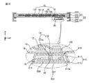
図1は、本実施例に係る太陽電池モジュールを示した概略的な斜視図であり、図2は、図1のII−II線に沿って切断した概略的な断面図である。そして、図3は、図1に示した太陽電池モジュールに含まれた太陽電池パネルの分解斜視図である。 FIG. 1 is a schematic perspective view showing a solar cell module according to the present embodiment, and FIG. 2 is a schematic cross-sectional view taken along line II-II in FIG. 3 is an exploded perspective view of the solar cell panel included in the solar cell module shown in FIG.
図1乃至図3を参照すると、本実施例に係る太陽電池モジュール100は、太陽電池12を含む太陽電池パネル10、及び太陽電池パネル10に接続され、太陽電池パネル10に装着される配線箱30を含む。太陽電池モジュール100は、太陽電池パネル10の外郭部を固定するフレーム20、太陽電池パネル10とフレーム20との間に位置し、これらを密封及び接着する接着部材などがさらに位置することができる。簡略且つ明確な図示のために、接着部材は図示しない。
Referring to FIGS. 1 to 3, a
太陽電池パネル10は、少なくとも1つの太陽電池12を含む。そして、太陽電池パネル10は、太陽電池12を包んで密封する密封層14と、密封層14の一面上で太陽電池12の前面に位置する前面基板16と、密封層14の他面上で太陽電池12の後面に位置する後面基板18とを含むことができる。
The
一例として、太陽電池12と、半導体基板(例えば、単結晶半導体基板、より具体的には、単結晶シリコンウエハ)と、半導体基板に又は半導体基板上に形成され、互いに反対の導電型を有する第1及び第2導電型領域と、これらにそれぞれ接続される第1及び第2電極とを含むことができる。ここで、第1及び第2導電型領域のうち一方はp型を有することができ、他方はn型を有することができる。そして、第1又は第2導電型領域は、半導体基板の一部にドーパントをドープして形成されるドーピング領域からなってもよく、または半導体基板上に別途に形成され、ドーパントがドープされた半導体層からなってもよい。そして、太陽電池12が複数備えられ、太陽電池12の第1電極とこれに隣接する太陽電池12の第2電極とはリボン122などによって接続されて、複数個の太陽電池12が一つの列をなす太陽電池ストリング(string)を形成することができる。太陽電池ストリングは、リボン122などによって、太陽電池パネル10の後面に位置した配線箱30に接続されてもよい。太陽電池12の構造、複数の太陽電池12の接続構造、太陽電池パネル10と配線箱30との接続構造などは、公知の様々な構造が適用されてもよい。
As an example, a
このように、本実施例では、太陽電池12としてシリコン半導体太陽電池を使用する場合を例示した。しかし、本発明がこれに限定されるものではなく、薄膜太陽電池、染料感応太陽電池、タンデム型太陽電池、化合物半導体太陽電池などの様々な構造の太陽電池を太陽電池12として使用することができる。そして、複数個の太陽電池12を備え、最外郭に位置した太陽電池12と太陽電池パネル10の縁部との間、及び隣り合う太陽電池12の間に外郭領域OAが位置する場合を例示したが、一つの太陽電池12のみを備え、太陽電池12と太陽電池パネル10の縁部との間にのみ外郭領域OAが位置してもよい。
Thus, in this example, the case where a silicon semiconductor solar cell is used as the
密封層14は、配線材122によって接続された太陽電池12の前面に位置する第1密封層14a、及び太陽電池12の後面に位置する第2密封層14bを含むことができる。第1密封層14a及び第2密封層14bは、水分と酸素が流入することを防止し、太陽電池パネル10の各要素を化学的に結合する。第1及び第2密封層14a,14bは、透光性及び接着性を有する絶縁物質で構成することができる。一例として、第1密封層14a及び第2密封層14bには、エチレン酢酸ビニル共重合体樹脂(EVA)、ポリビニルブチラール、ケイ素樹脂、エステル系樹脂、オレフィン系樹脂などが使用されてもよい。第1及び第2密封層14a,14bを用いたラミネーション工程などにより、後面基板18、第2密封層14b、太陽電池12、第1密封層14a、前面基板16が一体化されて太陽電池パネル10を構成することができる。
The
前面基板16は、第1密封層14a上に位置して太陽電池パネル10の前面を構成し、後面基板18は、第2密封層14b上に位置して太陽電池12の後面を構成する。前面基板16及び後面基板18は、それぞれ外部の衝撃、湿気、紫外線などから太陽電池12を保護できる絶縁物質で構成することができる。そして、前面基板16は、光が透過し得る透光性物質で構成され、後面基板18は、透光性物質、非透光性物質、または反射物質などで構成されるシートで構成されてもよい。一例として、前面基板16がガラス基板などで構成されてもよく、後面基板18が、TPT(Tedlar/PET/Tedlar)タイプを有するか、またはベースフィルム(例えば、ポリエチレンテレフタレート(PET))の少なくとも一面に形成されたポリフッ化ビニリデン(poly vinylidene fluoride、PVDF)樹脂層を含むことができる。
The
しかし、本発明がこれに限定されるものではない。したがって、第1及び第2密封層14a,14b、前面基板16、または後面基板18が、上述した説明以外の様々な物質を含むことができ、様々な形態を有することができる。例えば、前面基板16又は後面基板18が、様々な形態(例えば、基板、フィルム、シートなど)又は物質を有することができる。
However, the present invention is not limited to this. Accordingly, the first and second sealing layers 14a and 14b, the
上述したように、複数の層で構成された太陽電池パネル10を安定的に固定するために、太陽電池パネル10の外郭部が固定されるフレーム20が位置することができる。図面では、太陽電池パネル10の外郭部全体がフレーム20に固定される場合を示しているが、本発明がこれに限定されるものではない。したがって、フレーム20が太陽電池パネル10の一部の縁部だけを固定するなどの様々な変形が可能である。
As described above, in order to stably fix the
本実施例において、フレーム20は、太陽電池パネル10の少なくとも一部が挿入されるパネル挿入部22、及びパネル挿入部22から外部に向かって延びる延長部24を含むことができる。
In the present embodiment, the
より具体的に、パネル挿入部22は、太陽電池パネル10の前面に位置した前面部分222、太陽電池パネル10の側面に位置した側面部分224、太陽電池パネル10の後面に位置した後面部分226が互いに連結され、その内部に太陽電池パネル10の外郭部が位置するようにすることができる。一例として、パネル挿入部22は、2回折り曲げられて内部に太陽電池パネル10の縁部が位置するようにする、”逆コ”字断面形状または“U”字状を有することができる。しかし、本発明がこれに限定されるものではなく、前面部分222、側面部分224及び後面部分226のいずれか1つまたは一部が位置しなくてもよい。その他にも様々な変形が可能である。
More specifically, the
パネル挿入部22から後方に延びる延長部24は、パネル挿入部22から後方に向かって延び、側面部分224と平行に形成される(又は側面部分224と同一平面上に形成される)第1部分242と、第1部分242から折り曲げられて延びて太陽電池パネル10の後面又は後面部分226と一定間隔を置いて形成される第2部分244とを含むことができる。第2部分244は、太陽電池パネル10の後面又は後面部分226と平行に又は傾斜して形成されてもよい。これによって、延長部24は、1回折り曲げられて形成されて後面部分226との間に空間を形成する、“└”字状または“L”字断面形状を有することができる。
The
このような延長部24は、フレーム20の強度を増加させ、架台、支持体または底面などに固定される部分と連結される部分であって、延長部24には、架台、支持体、または底面との締結のための締結部材(図示せず)が締結されるホールが形成されてもよい。このように、太陽電池パネル10と離隔した第2部分244に締結部材などを締結するので、締結部材を用いた太陽電池モジュール100の設置時に太陽電池パネル10が損傷することを防止することができる。
The
締結部材などを安定的に固定できるように、第2部分244は、後面部分226と同一又はこれより大きい面積を有するように(すなわち、同一又はさらに大きい幅を有するように)形成することができる。そして、締結部材の構造などは、公知の様々な構造を使用することができる。本発明がこれに限定されるものではなく、延長部24がその他の様々な形状を有することができる。
The
このようなフレーム20は、様々な方法で太陽電池パネル10に固定することができる。一例として、太陽電池パネル10の外郭部をなす部分を、弾性を有する部分(一例として、弾性を有するテープ)として形成し、この弾性を有する部分を用いてパネル挿入部22内に太陽電池パネル10を挿入することができる。しかし、本発明がこれに限定されるものではなく、フレーム20を構成する部分を太陽電池パネル10の外郭部で組み立てて結合するなど、様々な変形が可能である。
Such a
そして、太陽電池パネル10の後面には、太陽電池パネル10に接続される配線を含む配線箱30を備えることができる。本実施例では、配線箱30が従来のジャンクションボックスの少なくとも一部とインバータの少なくとも一部とを一体化した構造を有する場合を例示した。このような配線箱30は、一体型インバータ、ジャンクションボックス一体型インバータ、バイパスダイオード一体型インバータ、一体型ジャンクションボックス、インバータ一体型ジャンクションボックスなどと命名してもよい。このような配線箱30を、図1乃至図3と共に図4を参照してより詳細に説明する。
And the
図4は、図1に示した配線箱30及び太陽電池パネル10の一部を概略的に示した分解斜視図である。
FIG. 4 is an exploded perspective view schematically showing a part of the
図1乃至図4を参照すると、本実施例に係る配線箱30は、配線箱30で異常信号があるとき、太陽電池パネル10を通して太陽電池パネル10の前面に光を放出する光源40が備えられる。そして、少なくとも配線箱30において太陽電池パネル10と光源40との間に位置する部分が、透光性を有する透光部TAからなる。本明細書において、透光性は、透明、半透明だけでなく、不透明であっても光があるか否かを区別できる程度を全て含むものである。そして、透光性を有しないということは、光があるか否かを判別できないことを意味する。
1 to 4, the
より具体的に、配線箱30は、内部に収容空間を備えるケース310を含み、ケース310の内部に位置し、太陽電池パネル10との電気的接続のための様々な配線部を含む回路部320を含むことができる。本実施例において、光源40の少なくとも一部がケース310の内部に位置することができる。すると、ケース310によって光源40が保護された状態で位置し、光源40を保護するための別途の構造を必要としない。また、配線箱30において光源40と太陽電池パネル10との間に位置する部分に透光部TAを形成することによって、光源40から放出された光が配線箱30及び太陽電池パネル10を通過して太陽電池パネル10の前面で認識され得る。すなわち、簡単な構造で、太陽電池パネル10の前面で認識できる光を排出するように光源40を安定的に配置することができる。
More specifically, the
これとは異なり、光源40がケース310の外部に位置する場合、光源40が外部衝撃、湿気などにより容易に損傷したり、ケース310から分離されるなどの問題が発生することがある。また、光源40全体がケース310の外部で太陽電池パネル10と配線箱30との間に位置する場合、光源40の構造的安定性を確保しにくく、太陽電池モジュール100の厚さが増加することがある。または、光源40が太陽電池パネル10の前面に位置する場合、雨、汚染物質、外部衝撃などにより、光源40が容易に損傷または破損することがある。これを防止するために別途に防水、緩衝構造などを形成する場合、太陽電池モジュール100の構造が非常に複雑になり、製造コストが増加することがある。
On the other hand, when the
光源40は、少なくとも一部がケース310の内部に位置しながら、ケース310に又はケース310の内部に固定され得る。一例として、光源40は回路部320に固定されてもよい。このように光源40が回路部320に固定されると、光源40を安定的に固定することができ、回路部320の配線に光源40を電気的に接続して、光源40の駆動(すなわち、オン/オフ(on/off))のための構造を単純化することができる。特に、本実施例では、回路部320が回路基板327(一例として、印刷回路基板)を備えることができ、光源40が回路基板327に固定されてもよい。これについては、より詳細に後述する。
The
しかし、本発明がこれに限定されるものではなく、光源40は様々な位置に固定されてもよい。一例として、光源40がケース310に固定されてもよく、ケース310と回路部320との間に固定されてもよく、その他の様々な変形が可能である。
However, the present invention is not limited to this, and the
ケース310は、内部収容空間を備え、回路部320、光源40などを保護できる様々な構造を有することができる。本実施例では、ケース310が、互いに接合されて一体のケースを形成する第1ケース部分311及び第2ケース部分312を含む場合を例示した。これによって、第1ケース部分311と第2ケース部分312が分離された状態では、内部に位置する回路部320及び光源40の挿抜が容易に行われるようにし、第1ケース部分311と第2ケース部分312が結合された状態では、内部に位置した回路部320及び光源40を安定的に収容することができる。しかし、本発明がこれに限定されるものではなく、ケース310の構造は様々に変形可能である。
The
一例として、第1ケース部分311は、太陽電池パネル10の後面に隣接して位置する底面を有しながら、内部収容空間を有する部分であり、第2ケース部分312が、内部収容空間を覆うように扁平な形状を有することができる。しかし、本発明がこれに限定されるものではない。したがって、第1ケース部分311が、扁平な形状を有しながら、太陽電池パネル10の後面に隣接して位置する底面で構成され、第2ケース部分312が、内部収容空間を有する部分であってもよい。第1ケース部分311と第2ケース部分312は、これらの縁部を接合及び密封する接合部材314によって互いに結合されてもよい。このような接合部材によって、外部から不純物、汚染物質などが流入することを防止し、密封特性及び防水特性を向上させることができる。接合部材314には、接合及び/又は密封特性を有する様々な物質を使用することができ、一例として、シーラント(シーリング材)などを使用することができる。しかし、本発明がこれに限定されるものではない。
As an example, the
ケース310は、外部形状又は外郭面を維持し、内部に位置した様々な部品、物品、部材などを保護し得る、様々な物質を含むことができる。一例として、ケース310は、樹脂、金属、表面処理された金属(又はコーティング処理された金属)などのような様々な物質で構成することができる。ケース310を絶縁物質(一例として、樹脂)で形成すると、絶縁特性を向上させ、コストを低減することができる。そして、ケース310が金属を含む場合、構造的安定性を高め、ケース310を接地などに使用することができる。このとき、ケース310が表面処理された金属(又はコーティング処理された金属)からなる場合、内部には、伝導性を有する物質が位置し、外部には、これを包み、絶縁特性を有する物質が位置し得る。これによって、絶縁物質によって耐腐食性を向上させ、外観を向上させることができ、内部に位置する金属物質を接地構造などに応用することができる。一例として、ケース310は、陽極酸化(anodizing)処理された金属(例えば、陽極酸化処理されたアルミニウム)からなることができる。そして、表面処理(一例として、陽極酸化処理)時にケース310の色相を共に調節して、外観をより一層向上させることができる。例えば、ケース310が黒色、褐色、銀色などの色相を有することができる。
The
このように、ケース310は、構成物質に応じて、透光性を有する物質で構成されたり、透光性を有しない物質で構成されてもよい。ケース310が透光性を有しない物質で構成される場合には、少なくとも光源40が位置する部分に対応する第1ケース部分311が透光性を有しなければならない。これは、第1ケース部分311は、光源40と太陽電池パネル10との間に位置して、光源40の光を遮断できる部分に位置するためである。これについては、回路部320を説明した後、透光部TAを説明するときにより詳細に説明する。
As described above, the
ケース310の内部に位置する回路部320は、太陽電池12又は太陽電池パネル10から延びて第1開口部(又は第1貫通部)310aを通過したリボン122が接続される端子321、端子321とインバータ部材325との間に位置したバイパスダイオード323、直流−交流インバータ325aを含むインバータ部材325、及び端子321、バイパスダイオード323、インバータ部材325などが位置する回路基板327のうちの少なくとも1つを含むことができる。そして、回路部320は、回路部320の各構成から状態情報を受けて各構成を制御し、異常信号がある場合に光源40の動作を制御する制御部329を備える。制御部329には、公知の様々な構成が適用され得、一例として、マイクロコントローラ(micro controller unit、MCU)が使用されてもよい。端子321、バイパスダイオード323、インバータ部材325及び制御部329は、回路基板327に形成された回路パターンによって接続され得る。
The
このとき、ケース310の内部において回路部320が位置していない空間は、ポッティング部材330(又は絶縁物質)で充填されたり、絶縁部、絶縁ケースなどが位置したりして、配線箱30の内部の気密性を向上させ、回路部320が不所望に短絡することを防止することができる。しかし、本発明がこれに限定されるものではなく、配線箱30の内部にポッティング部材330、絶縁物質、絶縁部、絶縁ケースなどが位置しなくてもよい。
At this time, the space where the
一例として、本実施例では、端子321、バイパスダイオード323、インバータ部材325及び制御部329が、回路パターン(又は回路、配線)を有する回路基板327上に共に形成される。これによって、端子321、バイパスダイオード323、インバータ部材325及び制御部329が回路基板327によって一体化されると見なすことができる。そして、回路基板327を覆うか又は包みながらポッティング部材330が位置し得、ポッティング部材330によってバイパスダイオード323、インバータ部材325及び制御部329が回路基板327に一体化されると見なすこともできる。また、端子321、バイパスダイオード323、インバータ部材325及び制御部329が形成された回路基板327は、同一のケース310の内部に位置することができる。これによって、端子321、バイパスダイオード323、インバータ部材325、制御部329及び回路基板327が同一のケース310によって一体化されると見なすこともできる。
As an example, in this embodiment, the terminal 321, the
インバータ部材325は、直流電流を交流電流に切り替える直流−交流インバータ325a、直流電流を交流電流に安定的に切り替えるためのキャパシタ325b、直流−直流コンバータ325cなどを含むことができる。
The
キャパシタ325bは、バイパスダイオード323を通過した電流を格納して、一定の電圧の電流を直流−直流コンバータ325cに伝達する。直流−直流コンバータ325cは、キャパシタ325bから受けた電圧の電流を一定水準の他の直流電圧に変換する。直流−交流インバータ325aは、直流−直流コンバータ325cから受けた直流電流又は直流電圧を交流電流又は交流電圧に変換する。このように配線箱30で生成された交流電流又は交流電圧は、インバータ部材325に接続され、ケース310の第2開口部(又は第2貫通部)310bを通過する交流出力ケーブル320aによって外部に伝達される。例えば、交流出力ケーブル320aによって他の太陽電池モジュール100と接続されるか、または電力網、電力系統などに伝達される。
The capacitor 325b stores the current that has passed through the
本実施例において、直流−直流コンバータ325cは複数個備えることができる。このように、直流−直流コンバータ325cを複数個備える場合、一つの直流−直流コンバータ325cを備える場合に比べて各直流−直流コンバータ325cの厚さを減少させることができ、これによって、配線箱30の厚さを延長部24の高さよりも小さくすることができる。しかし、本発明がこれに限定されるものではなく、直流−直流コンバータ325cを一つ備えることも可能である。
In this embodiment, a plurality of DC-
直流−交流インバータ325a、キャパシタ325b、及び直流−直流コンバータ325cには、公知の様々な構造が適用されてもよい。その他にも、フィルター部、通信部などの様々な部品が回路基板327上に位置することができる。
Various known structures may be applied to the DC-
本実施例において、リボン122と接続される端子321及び/又はバイパスダイオード323が位置する配線箱30から出力される出力ケーブルが交流出力ケーブル320aで構成され、直流出力ケーブルを備えない。これは、端子321及び/又はバイパスダイオード323とインバータ部材325を一体化したためである。従来は、端子及びバイパスが位置するジャンクションボックスから直流電圧又は直流電流を引き出すため、(+)出力ケーブル及び(−)出力ケーブルの2つの直流出力ケーブルが存在するようになる。
In the present embodiment, the output cable output from the
本実施例において、ケース310には、太陽電池パネル10との接続のための構造、及び外部(例えば、他の太陽電池モジュール100又は電力網)などとの接続のための構造が共に形成されてもよい。すなわち、ケース310には、リボン122が通過する部分で一部が除去されて形成された第1開口部310a、及び配線箱30によって生成された交流電流(又は、交流電圧、電流電力、交流電源)を伝達する一つの交流出力ケーブル320aが通過する第2開口部310bを備えることができる。すなわち、太陽電池パネル10との接続のための第1開口部310a及び交流出力ケーブル320aのための第2開口部310bが同一のケース310に形成される。これは、端子321及び/又はバイパスダイオード323とインバータ部材325を一体化したためである。
In the present embodiment, the
上述したようなケース310は、接着部材316によって太陽電池パネル10の後面に固定され得る。また、接着部材316は、第1開口部310aを取り囲みながら内部に閉鎖空間(closed space)を備え、接着部材316の内部空間を外部と隔離する。これによって、外部物質、湿気、不純物などが第1開口部310aを通してケース310の内部に流入することを防止することができる。これによって、ケース310の気密特性、密封特性及び防水特性を向上させることができる。
The
接着部材316には、優れた接着特性、密封特性などを有する様々な物質を使用することができる。一例として、接着部材316としてシーラント(シーリング材)などを使用することができる。しかし、本発明がこれに限定されるものではない。したがって、接着部材316が樹脂、金属などで形成された構造物で構成され、熱などによってケース310と太陽電池パネル10を接着するなど、様々な変形が可能である。また、他の結合構造(例えば、ねじ結合、ラッチ構造、パッキング構造)によってケース310と太陽電池パネル10を固定することもできる。その他の様々な変形が可能である。
For the
本実施例では、端子321、バイパスダイオード323、インバータ部材325及び回路基板327を一つの配線箱30内に共に位置させることで、設置工程を単純化し、構造を簡単にすることができる。そして、光源40によって、様々な太陽電池モジュール100の状態情報を表示することができる。しかし、本発明がこれに限定されるものではなく、配線箱30は、端子321、バイパスダイオード323、インバータ部材325及び回路基板327のうちの少なくとも1つを備える全ての構成を意味し得る。例えば、配線箱30が、太陽電池パネル10のリボン122に接続される端子321及び/又はバイパスダイオード323を備えるジャンクションボックスと、インバータ部材325を含むインバータボックスとを別個に備えることができ、ジャンクションボックス及びインバータボックスのうちの少なくとも1つが、上述したような光源40及び透光部TAを備えることができる。及び/又は、配線箱30がパワーオプティマイザ(power optimizer)、モジュールレベルパワーエレクトロニクス(module level power electronics、MLPE)などを含むことができ、そのうちの少なくとも1つが、上述したように光源40及び透光部TAを備えることができる。
In the present embodiment, the terminal 321, the
再び光源40及び透光部TAを説明する。本実施例において、光源40は、回路基板327上で太陽電池パネル10に向かう面に位置することができる。これによれば、光源40から放出された光が短い経路で太陽電池パネル10に到達するため、光伝達の効率を向上させることができる。また、回路基板327に含まれる回路パターンによって、光源40に必要な電源、信号などを容易に供給することができる。一例として、光源40の端子が、半田付けなどのような方法により、印刷回路基板327の回路配線に電気的及び物理的に接続されてもよい。このとき、光源40を駆動するための電源として、別途に提供される電源を使用してもよく、太陽電池パネル10で生成された電源の一部を使用してもよい。しかし、本発明がこれに限定されるものではなく、光源40の位置は様々な変形が可能である。
The
このとき、平面上で、光源40は、太陽電池パネル10において太陽電池12が位置していない部分、すなわち、太陽電池パネル10の縁部及び隣り合う太陽電池12の間に対応する外郭領域OAに対応するように位置する。太陽電池12が位置した部分に対応して光源40が位置する場合、光源40から放出された光が太陽電池12によって遮られて前面で認識することが難しいためである。特に、光源40は、太陽電池パネル10でよく見えるように、隣り合う太陽電池12の間に位置する外郭領域OAに対応するように位置し得る。太陽電池パネル10の縁部は、フレーム20などによって少なくとも一部が遮られているため、光源40による光を認識することが難しいためである。
At this time, on the plane, the
しかし、本発明がこれに限定されるものではない。すなわち、光源40が太陽電池12に対応して位置しても、光源40の光の一部が外郭領域OAを通して太陽電池パネル10の前面に到達することができれば、光源40が太陽電池12に対応して位置することもできる。
However, the present invention is not limited to this. That is, even if the
光源40は、公知の様々な構造、方式などで光を放出することができる。一例として、光源40は、小さい体積を有し、経済的であり、環境に優しい発光ダイオード(light emitting diode、LED)を含むことができる。
The
このとき、少なくとも光源40と太陽電池パネル10との間に位置する配線箱30の部分が透光部TAで構成される。一例として、本実施例では、配線箱30のケース310(より具体的には、第1ケース部分311の底面)において、光源40が位置した部分に対応して貫通孔310cが形成される。すると、ケース310が透光性を有するか否かに関係なく、貫通孔310cを通して光が透過し得る。これによって、このような貫通孔310cが透光部TAを構成することができる。
At this time, at least a portion of the
このように、貫通孔310cを形成して透光部TAを形成すると、貫通孔310cを形成する簡単な工程により透光部TAを形成することができる。そして、貫通孔310cは、光を高い透過率で透過させるため、太陽電池パネル10の前面で光源40から放出された光を明確に認識するようにすることができる。特に、ケース310が不透明な場合に、貫通孔310cによって光が透過し得るようにすることができる。
Thus, if the through-
このとき、貫通孔310cは、透光性を有する透光物質318(例えば、樹脂)などで埋められ、配線箱30の気密性が低下しないようにすることができる。透光物質318は、流動性を有する物質を貫通孔310cを塞ぐように塗布した後、乾燥、硬化などによって固めることによって形成することができる。
At this time, the through-
このとき、透光物質318も、光源40と太陽電池パネル10との間に位置するため、透光物質318が透光部TAの一部を構成するようになる。しかし、透光物質318は必須のものではない。したがって、ケース310の内部にポッティング部材330、絶縁部などが位置すると、貫通孔310cを別途の物質で埋めなくてもよい。または、図示のように、接着部材316が貫通孔310cを取り囲む閉鎖された空間を備えるように形成されると、貫通孔310cを別途の物質で埋めなくてもよい。そして、図面では、光源40上に透光物質318のみが位置する場合を例示したが、光源40上にポッティング部材330と透光物質318が共に位置するか、または透光物質318なしにポッティング部材330のみが位置してもよい。この場合には、ポッティング部材330も透光性を有することで、透光部TAの一部を構成することができる。または、光源40と太陽電池パネル10との間に空き空間が位置することもでき、この場合には、空き空間も透光性を有するため、透光部TAの一部を構成することができる。
At this time, since the
図面において、光源40に対応する貫通孔310cは、リボン122が通過する第1開口部310aと異なる別個のホールである場合を例示した。これによれば、光源40が位置する部分とリボン122が通過する部分とを別個の位置に位置させ、リボン122などによって光が太陽電池パネル10の前面側に到達することが妨げられることを防止することができる。しかし、本発明がこれに限定されるものではなく、図5に示したように、リボン122が通過する第1開口部310a内に光源40が位置できるようにして、別途の貫通孔310cを形成せず、リボン122が通過する第1開口部310aを貫通孔310cとして使用することができる。すると、ケース310に貫通孔310cを形成しなくてもよいので、ケース310の構造を単純化することができる。また、別途に透光物質318を備えなくてもよい。しかし、本発明がこれに限定されるものではなく、様々な変形が可能である。
In the drawing, the case where the through
このように、本実施例では、光源40が位置する部分に対応して部分的に形成された貫通孔310cが透光部TAを構成する場合を例示した。これによれば、従来使用していたケース310(より具体的には、回路基板327と太陽電池パネル10との間に位置する第1ケース部分311)に貫通孔310cを形成することによって、容易に透光部TAを形成することができる。しかし、本発明がこれに限定されるものではない。他の実施例については、図9乃至図13を参照してより詳細に後述する。
Thus, in the present embodiment, the case where the through
以下では、太陽電池モジュール100または配線箱30に異常信号があるときに光源40が光を放出する原理を、図6を参照して詳細に説明する。図6は、図1に示した太陽電池モジュールにおける配線箱30及び光源40の回路図の一例である。明確且つ簡略な図示のために、図6では、端子321、バイパスダイオード323、キャパシタ325bなどの図示を省略し、光源40の制御のための部分を中心に説明した。
Hereinafter, the principle that the
図6を参照すると、太陽電池パネル10で生成された直流電流、直流電圧、または直流電源がインバータ部材325に伝達される。インバータ部材325の直流−直流コンバータ325cでは、直流電流、直流電圧、または直流電源を、異なる値を有する直流電流、直流電圧、または直流電源に変換する。インバータ部材325の直流−交流インバータ325aでは、直流−直流コンバータ325cから受けた直流電流、直流電圧、または直流電源を、交流電流、交流電圧、または交流電源に変換する。このように変換された交流電流、交流電圧、または交流電源は、交流出力ケーブル320aを介して外部に伝達される。
Referring to FIG. 6, the direct current, direct current voltage, or direct current power generated by the
このとき、制御部329は、インバータ部材325から状態情報を受け、状態情報に応じてインバータ部材325を制御する信号を送信してインバータ部材325を制御する。このとき、制御部329がインバータ部材325の異常信号(すなわち、太陽電池モジュール100の異常信号)を発見した場合には、これに合わせてインバータ部材325の動作を制御しながら、光源40に光源動作制御信号を送信して、光源40の動作(一例として、オン/オフ)を制御する。すると、光源40は、光を太陽電池パネル10の前面に放出する。すると、使用者又は管理者は、太陽電池パネル10の前面で光を認識し、インバータ部材325又は太陽電池パネル10に異常があることを感知することができる。
At this time, the
光源40は、単純にオン/オフによって、太陽電池モジュール100(又はインバータ部材325)の動作が正常であるか、または異常があるかを知らせることができる。例えば、太陽電池モジュール100が正常作動する場合には、光源40がオフ状態を維持し、太陽電池モジュール100に異常がある場合には、光源40がオンされ得る。または、太陽電池モジュール100の様々な動作異常に応じて異なる時間間隔、異なる色、または異なる強度で光を提供して、太陽電池モジュール100のどの部分に異常があるかを具体的に知らせることもできる。
The
光源40を用いて表示できる太陽電池モジュール100の異常は、様々な種類があり得る。例えば、インバータ部材325から出力される交流電流の周波数(AC Frequency)が設定基準よりも速く変化する場合、漏洩電流が設定基準よりも高い場合、インバータ部材325から出力される交流電流が設定基準よりも高い場合、入ってくる直流電流が設定基準よりも高い場合、回路部320の通信部の通信が安定していない場合、インバータ部材325が作動しない場合、インバータ部材325の温度が設定基準よりも高い場合、インバータ部材325から出力される交流電圧が設定基準よりも高い又は低い場合、インバータ部材325から出力される交流電流の周波数が設定基準よりも高い又は低い場合、インバータ部材325に入力される直流電圧が設定基準よりも高い又は低い場合に、光源40が光を放出することができる。その他の様々な種類の異常を、光源40を介して表示することができる。
There are various types of abnormalities in the
本実施例によれば、光源40から放出されて太陽電池パネル10を貫通して太陽電池パネル10の前面に到達する光を、使用者又は管理者が目視で認識することによって、太陽電池モジュール100の異常又は動作不良を感知することができる。または、太陽電池パネル10の前面まで到達した光を感知する別途の異常感知装置(図7の参照符号200、以下同様)を用いて、太陽電池モジュール100の異常又は動作不良を感知することもできる。このように、本実施例では、太陽電池モジュール100の異常信号を太陽電池モジュール100自体で知ることができるので、太陽電池モジュール100の異常を容易に感知し、これに必要な措置を取ることができる。これによって、太陽電池モジュール100の管理をより円滑に行うことができる。
According to the present embodiment, the
異常感知装置200を用いると、時間間隔、色、または強度が微細に制御された光源40の光信号を感知し、太陽電池モジュール100の様々な異常又は動作不良のうちどのような異常又は動作不良が発生したかをより具体的に知ることができる。図1乃至図6と共に、図7及び図8を参照して、本実施例に係る太陽電池モジュール100に使用可能な異常感知装置200を詳細に説明する。
When the
図7は、本発明の実施例に係る太陽電池モジュール100に使用可能な異常感知装置200を示した斜視図であり、図8は、図7に示した異常感知装置200の概略的な回路図である。
FIG. 7 is a perspective view illustrating an
図7及び図8を参照すると、本実施例に係る異常感知装置200は、光センサ202、制御部204及び表示部206を含むことができる。
Referring to FIGS. 7 and 8, the
光センサ202は、光源40から放出されて太陽電池パネル10の前面まで到達した光を認識する。これによって、光センサ202は、光信号を受信し、これを電気信号に変換して制御部204に伝達する。光センサ202は、本体210の一側端部に位置し得る。すると、太陽電池パネル10の前面側に、光センサ202が位置する本体210の一側端部を位置させることによって、正確に光信号を認識することができる。光センサ202としては、公知の様々な構造のセンサを適用することができる。
The
制御部204は、光センサ202から伝達された電気信号に応じて、表示部206に表示されるべき内容が表示されるようにする制御信号を表示部206に伝達する。制御部204は、本体210の内部に位置することができる。
The
表示部206は、本体210において最も広い面に位置し、異常信号を表示することができる。このとき、表示部206に表示される異常信号は、単に異常信号があることを知らせるものであってもよく、具体的にどのような異常信号があるかを知らせるものであってもよい。表示部206には、公知の様々な構成が適用されてもよく、一例として、異常信号を文字などで表示する液晶表示装置などが適用されてもよい。または、光源40の信号を光の強度、色などで表示することもできる。
The
このように、異常感知装置200によると、光源40から放出される光のオン/オフ、光源40の点灯回数、光源40の点灯時間間隔、光源40から放出される光の色、及び/又は光源40から放出される光の強度の微細な差を光センサ202が認識することができ、これに基づいて、異常信号による表示が表示部206で行われるので、太陽電池モジュール100の具体的な状態を明確に知ることができる。
As described above, according to the
以下、図9乃至図13を参照して、本発明の他の実施例に係る太陽電池モジュールを詳細に説明する。上述した部分で説明したものと同一又は類似の部分については詳細な説明を省略し、異なる部分を詳細に説明する。そして、上述した実施例及びその変形例と、以下の実施例及びその変形例とは互いに結合されてもよく、これもまた本発明の範囲に属する。 Hereinafter, a solar cell module according to another embodiment of the present invention will be described in detail with reference to FIGS. 9 to 13. Detailed description of the same or similar parts as those described in the above part will be omitted, and different parts will be described in detail. The above-described embodiment and its modifications may be combined with the following embodiments and their modifications, which also belong to the scope of the present invention.
図9は、本発明の他の実施例に係る太陽電池モジュールを示した部分断面図である。参考に、図9では、図2の拡大円に対応する部分を示した。 FIG. 9 is a partial cross-sectional view illustrating a solar cell module according to another embodiment of the present invention. For reference, FIG. 9 shows a portion corresponding to the enlarged circle of FIG.
図9を参照すると、本実施例では、光源40と太陽電池パネル10との間に位置するケース310の部分が、全体的に透光性を有する物質(一例として、透明又は半透明な樹脂など)で構成される透光部分311aからなることができる。透光性を有するケース310の少なくとも一部自体が透光部TAを構成することができる。したがって、別途の貫通孔(図2の参照符号310c)及び/又は透光物質(図2の参照符号318)を備えなくてもよい。このとき、図9では、第1ケース部分311が全体的に透光部分311aで構成された場合を例示したが、本発明がこれに限定されるものではない。
Referring to FIG. 9, in the present embodiment, the portion of the
したがって、図10に示したように、第1ケース部分311において光源40が位置する部分にのみ部分的に透光性を有する透光部分311aが位置して透光部TAを形成し、その他の部分は非透光部分311bからなることもできる。または、第1ケース部分311において太陽電池パネル10の後面に隣接する底面が全体的に透光部分311aで構成され、第1ケース部分311の側面部分、及び第2ケース部分312と隣接する部分が非透光部分311bで構成されてもよい。また、第1ケース部分311だけでなく、第2ケース部分312の少なくとも一部が透光部分を含むこともできる。すなわち、本実施例では、少なくとも太陽電池パネル10側に位置する面において光源40に対応する配線箱30(より具体的には、ケース310)の部分が、透光性を有する透光部分311aで構成されればよい。
Accordingly, as shown in FIG. 10, the
図9及び図10では、光源40が第1ケース部分311の透光部分311aに接して形成され、光源40と太陽電池パネル10との間に透光部分311aのみが位置する場合を例示した。しかし、本発明がこれに限定されるものではなく、光源40が透光部分311aと離隔して形成され、光源40と透光部分311aとの間に、透光性を有するポッティング部材330又は空き空間などが位置することができる。この場合には、光源40と透光部分311aとの間に位置する透光性を有するポッティング部材330又は空き空間が、透光部TAの一部を構成することができる。
9 and 10 exemplify the case where the
図11は、本発明の更に他の実施例に係る太陽電池モジュールを示した部分断面図である。参考に、図11では、図2の拡大円に対応する部分を示した。 FIG. 11 is a partial cross-sectional view illustrating a solar cell module according to still another embodiment of the present invention. For reference, FIG. 11 shows a portion corresponding to the enlarged circle of FIG.
図11を参照すると、本実施例では、光源40と太陽電池パネル10との間に位置して、光源40を覆い、透光性を有する蓋部42が位置することができる。蓋部42は、光源40を覆うことができるように、太陽電池パネル10に向かって膨らんだ形状を有する透光性構造物であってもよく、一例として、透明又は半透明な樹脂などで構成されてもよい。このような蓋部42を備えると、光源40を覆う蓋部42によって容易に透光部TAを形成することができる。
Referring to FIG. 11, in the present embodiment, a
一例として、蓋部42は、第1ケース部分311の貫通孔310cを貫通して太陽電池パネル10の後面基板18に接触することができる。このとき、蓋部42が貫通孔310cを全体的に満たすようにぴったり嵌合され得る。すると、構造的に安定して蓋部42を固定することができ、光源40を保護することができる。
As an example, the
しかし、本発明がこれに限定されるものではない。他の例として、第1ケース部分311が貫通孔310cを備えず、第1ケース部分311が透光部分(図9又は図10の参照符号311a)を備え、蓋部42がケース310の内部に位置することもできる。このとき、蓋部42は、第1ケース部分311に接触してもよく、又は、第1ケース部分311との間に、透光性を有するポッティング部材330又は空き空間などを介在して位置してもよい。
However, the present invention is not limited to this. As another example, the
図12は、本発明の更に他の実施例に係る太陽電池モジュールを示した部分断面図である。参考に、図12では、図2の拡大円に対応する部分を示した。 FIG. 12 is a partial cross-sectional view illustrating a solar cell module according to still another embodiment of the present invention. For reference, FIG. 12 shows a portion corresponding to the enlarged circle of FIG.
図12を参照すると、本実施例では、後面基板18が、少なくとも光源40に対応する配線箱30の部分に対応する部分で、透光性を有する透光部分18aで構成される。太陽電池パネル10において、前面基板16及び密封層14は透光性を有する物質で形成される。そして、光源40は、太陽電池12によって遮られない外郭領域OAに対応するように位置する。したがって、前面基板16、太陽電池12及び密封層14は、光源40から放出された光を遮らない。
Referring to FIG. 12, in this embodiment, the
後面基板18が全体的に透光性を有する場合には、光源40から放出された光を遮らない。一方、後面基板18は、場合によって、反射特性を向上させるための反射シート、または外観を向上させることができる黒色又は黒色シートなどで構成されて非透光部分18bを含むことができる。この場合には、光源40による光が後面基板18によって妨げられることがあるため、後面基板18において、光源40が位置する部分(すなわち、外郭領域OAの一部)に対応して透光部分18aが位置するようにする。
When the
このとき、図12に示したように、非透光部分18bを全体的に備える後面基板18に貫通孔180を形成して透光部分18aを形成することもできる。透光部分18aが貫通孔からなる場合、簡単な工程により透光部分18aを形成することができる。
At this time, as shown in FIG. 12, it is also possible to form the
または、図13に示したように、非透光部分18bを全体的に備える後面基板18に貫通孔180を形成した後、透光性を有する透光物質182(一例として、透明又は半透明な樹脂)で貫通孔180を埋めて透光部分18aを形成することができる。一例として、印刷などによって貫通孔180を埋めることができる。または、透光部分18aは、後面基板18の製造工程で透明又は半透明な樹脂などによって、非透光部分18bと共に製造されてもよい。これによれば、後面基板18が空き部分なしに全体的に位置し、後面基板18による効果を最大化することができる。
Alternatively, as shown in FIG. 13, after a through-
図12及び図13では、光源40に対応して貫通孔310cが形成され、透光物質318が備えられた場合を例示した。しかし、本発明がこれに限定されるものではなく、貫通孔310c及び/又は透光物質318が備えられないことも可能である。
12 and 13 exemplify the case where the through-
本実施例によれば、光源から放出されて太陽電池パネルを貫通して太陽電池パネルの前面に到達する光を、使用者又は管理者が目視で認識することによって、太陽電池モジュールの異常又は動作不良を感知することができる。または、太陽電池パネルの前面まで到達した光を感知する別途の太陽電池モジュール用異常感知装置を用いて、太陽電池モジュールの異常又は動作不良を感知することもできる。すると、太陽電池モジュールの異常信号を太陽電池モジュール自体で知ることができるため、太陽電池モジュールの異常を容易に感知し、これに必要な措置を取ることができる。これによって、太陽電池モジュールの管理をより円滑に行うことができる。 According to the present embodiment, the user or the manager visually recognizes the light emitted from the light source and penetrating the solar cell panel to reach the front surface of the solar cell panel, thereby causing the abnormality or operation of the solar cell module. Defects can be detected. Alternatively, an abnormality or malfunction of the solar cell module can be detected using a separate solar cell module abnormality sensing device that senses light reaching the front surface of the solar cell panel. Then, since the abnormality signal of the solar cell module can be known by the solar cell module itself, the abnormality of the solar cell module can be easily detected and necessary measures can be taken. Thereby, management of a solar cell module can be performed more smoothly.
このとき、太陽電池モジュール用異常感知装置を使用すると、光源から放出される光のオン/オフ、光源の点灯回数、光源の点灯時間間隔、光源から放出される光の色、及び/又は光源から放出される光の強度の微細な差による太陽電池モジュールの具体的な状態を明確に知ることができる。 At this time, when using the solar cell module abnormality sensing device, on / off of the light emitted from the light source, the number of times the light source is turned on, the lighting time interval of the light source, the color of the light emitted from the light source, and / or the light source It is possible to clearly know the specific state of the solar cell module due to a minute difference in the intensity of emitted light.
次いで、図14ないし図17を参照して、本発明の更に他の実施例に係る太陽電池モジュールを説明する。 Next, a solar cell module according to still another embodiment of the present invention will be described with reference to FIGS.
図14ないし図16は、本発明の更に他の実施例に係る太陽電池モジュールを示した概略的な断面図である。図17は、図14ないし図16に示された太陽電池モジュールの作動を説明するためのブロック図である。 14 to 16 are schematic cross-sectional views illustrating a solar cell module according to still another embodiment of the present invention. FIG. 17 is a block diagram for explaining the operation of the solar cell module shown in FIGS. 14 to 16.
本実施例に係る太陽電池モジュールは、図1乃至図3を参照して説明した太陽電池モジュールと比較して、光受信部をさらに含むこと以外は実質的に同一である。したがって、同一の参照番号は同一の構成要素を示し、繰り返される説明は省略できる。 The solar cell module according to the present embodiment is substantially the same as the solar cell module described with reference to FIGS. 1 to 3 except that it further includes an optical receiver. Accordingly, the same reference numerals indicate the same components, and repeated description can be omitted.
図14ないし図16を参照すると、本実施例に係る太陽電池モジュール100は、太陽電池12を含む太陽電池パネル10、及び太陽電池パネル10に接続され、太陽電池パネル10に装着される配線箱30を含む。太陽電池モジュール100は、太陽電池パネル10の外郭部を固定するフレーム20、太陽電池パネル10とフレーム20との間に位置し、これらを密封及び接着する接着部材などがさらに位置することができる。
14 to 16, a
太陽電池パネル10は、少なくとも1つの太陽電池12を含む。 光受信部19は、配線箱30と電気的に接続されるように構成されるか、または、配線箱30に直接形成することもできる。 例えば、光受信部19は、配線箱30の光源40側に位置することができる(図16)。
The
太陽電池パネル19は、光受信部19に入力された制御信号を介して制御することができる。つまり、光受信部19は、外部の制御部(図示せず)が含まれている光源(図示せず)からの光信号を受信することができ、受信された光信号を介して太陽電池パネル19を制御することができる。
The
すなわち、使用者は、端末などの入力装置を用いて、制御信号を利用して、光源(図示せず)から、特定の光信号を発生するようにすることができる。ここで、特定の光信号は、太陽電池パネル10の適正電圧、電流の周波数などの系統情報やその他にアレイビルディング(array building)に必要な情報であるか、またはその他の制御信号を含むことができる。
That is, the user can generate a specific optical signal from a light source (not shown) by using a control signal using an input device such as a terminal. Here, the specific optical signal may be system information such as an appropriate voltage and current frequency of the
これらの情報および制御信号を含む、特定の光信号は、光受信部19で受信することができ、光受信部19は、受信された特定の光信号に基づいて、太陽電池パネル10を制御することができる。
A specific optical signal including these information and control signals can be received by the
図15を参照すると、外部からの端末などを介して情報の入力が行われると、その情報に基づいて光サンゴが前記光源からの光受信部19に渡すことができる。光信号を受信された光受信部19は、受信した光信号に応じた制御信号を受信することができる。これにより, 太陽電池パネルの出力信号などを制御することができる。
Referring to FIG. 15, when information is input through an external terminal or the like, the optical coral can be passed to the
上述したような特徴、構造、効果などは、本発明の少なくとも一つの実施例に含まれ、必ずしも一つの実施例にのみ限定されるものではない。さらに、各実施例で例示した特徴、構造、効果などは、実施例の属する分野における通常の知識を有する者によって、他の実施例に対しても組み合わせ又は変形して実施可能である。したがって、このような組み合わせ及び変形に係わる内容は、本発明の範囲に含まれるものと解釈されるべきである。 Features, structures, effects, and the like as described above are included in at least one embodiment of the present invention, and are not necessarily limited to only one embodiment. Furthermore, the features, structures, effects, etc. exemplified in each embodiment can be implemented by combining or modifying other embodiments by those who have ordinary knowledge in the field to which the embodiment belongs. Therefore, contents relating to such combinations and modifications should be construed as being included in the scope of the present invention.
Claims (20)
前記太陽電池パネルの後面に位置し、前記太陽電池パネルと接続される配線を含む配線箱と、
異常信号が検出されたとき、前記太陽電池パネルを通して前記太陽電池パネルの前面に光を放出し, 前記配線箱に少なくとも一部が位置する光源と、
前記光源と前記太陽電池パネルとの間に位置し、前記光源を覆う透光性の蓋部を含み,
前記配線箱は、内部に収容空間を備えるケースを含み、
前記ケースは、前記太陽電池パネルの後面近くに位置する第1ケースと、前記第1ケースを覆う第2ケースを含み、
前記光源の少なくとも一部は、前記収容空間に光を照射するために前記ケースの中に位置する、太陽電池モジュール。 A solar panel,
A wiring box located on the rear surface of the solar cell panel and including wiring connected to the solar cell panel;
When an abnormal signal is detected, light is emitted to the front surface of the solar cell panel through the solar cell panel, and a light source at least partially located in the wiring box ;
Located between the light source and the solar cell panel , including a translucent lid that covers the light source ,
The wiring box includes a case having an accommodation space inside,
The case includes a first case located near the rear surface of the solar cell panel, and a second case covering the first case,
At least a part of the light source is a solar cell module positioned in the case for irradiating the accommodation space with light.
前記光源は、前記回路部に固定される、請求項3に記載の太陽電池モジュール。 The wiring box includes the wiring, and includes a circuit unit located inside the case.
The solar cell module according to claim 3, wherein the light source is fixed to the circuit unit.
前記光源は、前記印刷回路基板に固定される、請求項4に記載の太陽電池モジュール。 The circuit unit includes a printed circuit board,
The solar cell module according to claim 4, wherein the light source is fixed to the printed circuit board.
前記リボンが通過する第1開口部が前記配線箱に形成され、
前記第1開口部と前記貫通孔は、別個に形成される、請求項7に記載の太陽電池モジュール。 A ribbon extending from the solar panel;
A first opening through which the ribbon passes is formed in the wiring box;
The solar cell module according to claim 7, wherein the first opening and the through hole are formed separately.
前記蓋部は、前記貫通孔を貫通して前記太陽電池パネルに接触する、請求項1に記載の太陽電池モジュール。 In part of the portion of the case located between the light source and the solar cell panel, a through hole is formed corresponding to the position of the light source,
The solar cell module according to claim 1 , wherein the lid portion is in contact with the solar cell panel through the through hole.
前記光源の位置に対応する、前記後面基板の少なくとも一部は、透光部分を含む、請求項1に記載の太陽電池モジュール。 The solar cell panel includes a front substrate, a solar cell, a rear substrate, and a sealing layer,
The solar cell module according to claim 1, wherein at least a part of the rear substrate corresponding to the position of the light source includes a light-transmitting portion.
前記制御部は、前記インバータ部材の異常信号が検出される場合、前記光源をオン又はオフに制御する、請求項5に記載の太陽電池モジュール。 The circuit unit includes an inverter member and a control unit that receives state information of the inverter member and controls the inverter member and the light source,
The said control part is a solar cell module of Claim 5 which controls the said light source on or off, when the abnormal signal of the said inverter member is detected.
前記光源から放出された光が前記外郭領域を通して前記太陽電池パネルの前面に放出される、請求項1に記載の太陽電池モジュール。 The solar panel includes an outer shell region solar cell is not located,
The solar cell module according to claim 1, wherein light emitted from the light source is emitted to the front surface of the solar cell panel through the outer region.
前記光源が、複数の隣り合う太陽電池の間に位置した前記外郭領域の部分に対応して位置する、請求項15に記載の太陽電池モジュール。 The solar cell includes a plurality of solar cells;
The solar cell module according to claim 15 , wherein the light source is located corresponding to a portion of the outer region located between a plurality of adjacent solar cells.
前記太陽電池パネルの前面で外部の光源の光信号を検出し、前記光信号を電気信号に変換する光センサと、
前記電気信号を受信して前記電気信号を制御信号に変換する制御部と、
前記制御信号に応じて異常信号を表示する表示部と、
を含み、
前記配線箱は、内部に収容空間を備えるケースを含み、
前記ケースは、前記太陽電池パネルの後面近くに位置する第1ケースと、前記第1ケースを覆う第2ケースを含み、
前記光源の少なくとも一部は前記収容空間に光を照射するために前記ケースの中に位置する、太陽電池モジュール用異常感知装置。 A solar cell panel, a wiring box located on a rear surface of the solar cell panel, including a wiring box including wiring connected to the solar cell panel, and an abnormal signal is detected, the light is transmitted to the front surface of the solar cell panel through the solar cell panel An abnormality sensing device for a solar cell module used in a solar cell module including a light source that emits light,
An optical sensor for detecting an optical signal of an external light source on the front surface of the solar cell panel and converting the optical signal into an electrical signal;
A controller that receives the electrical signal and converts the electrical signal into a control signal;
A display unit for displaying an abnormal signal in response to the control signal;
Including
The wiring box includes a case having an accommodation space inside,
The case includes a first case located near the rear surface of the solar cell panel, and a second case covering the first case,
An abnormality sensing device for a solar cell module, wherein at least a part of the light source is located in the case for irradiating the accommodation space with light.
Applications Claiming Priority (2)
| Application Number | Priority Date | Filing Date | Title |
|---|---|---|---|
| KR10-2015-0122847 | 2015-08-31 | ||
| KR1020150122847A KR20170025831A (en) | 2015-08-31 | 2015-08-31 | Solar cell module and error detector for solar cell module |
Publications (2)
| Publication Number | Publication Date |
|---|---|
| JP2017051091A JP2017051091A (en) | 2017-03-09 |
| JP6416163B2 true JP6416163B2 (en) | 2018-10-31 |
Family
ID=56852130
Family Applications (1)
| Application Number | Title | Priority Date | Filing Date |
|---|---|---|---|
| JP2016170074A Active JP6416163B2 (en) | 2015-08-31 | 2016-08-31 | SOLAR CELL MODULE AND ABNORMALITY SENSING DEVICE FOR SOLAR CELL MODULE |
Country Status (5)
| Country | Link |
|---|---|
| US (1) | US10476430B2 (en) |
| EP (1) | EP3136595B1 (en) |
| JP (1) | JP6416163B2 (en) |
| KR (1) | KR20170025831A (en) |
| CN (1) | CN106487329A (en) |
Families Citing this family (5)
| Publication number | Priority date | Publication date | Assignee | Title |
|---|---|---|---|---|
| KR102337578B1 (en) * | 2017-06-21 | 2021-12-08 | 엘에스일렉트릭(주) | System for detection of photovoltaic module using the unmanned aerial vehicle |
| KR102615861B1 (en) * | 2018-07-25 | 2023-12-21 | 상라오 징코 솔라 테크놀러지 디벨롭먼트 컴퍼니, 리미티드 | Solar cell module |
| TWI736195B (en) * | 2020-03-30 | 2021-08-11 | 睿騰能源有限公司 | Battery detection system, detection method thereof, and optical decoding device |
| CN113535489A (en) * | 2020-04-22 | 2021-10-22 | 睿腾能源有限公司 | Battery detection system, detection method thereof and optical decoding device |
| CN113540582A (en) * | 2020-04-22 | 2021-10-22 | 睿腾能源有限公司 | Battery detection system, detection method thereof and battery device |
Family Cites Families (17)
| Publication number | Priority date | Publication date | Assignee | Title |
|---|---|---|---|---|
| JPS6370169U (en) * | 1986-10-24 | 1988-05-11 | ||
| KR100255105B1 (en) * | 1995-04-12 | 2000-05-01 | 마츠시타 덴끼 산교 가부시키가이샤 | Data processing method for generating error correction product code block, data processing method for recording data in recording medium, and data processing device for data |
| JP3349317B2 (en) | 1995-11-24 | 2002-11-25 | 三洋電機株式会社 | Solar cell module |
| JPH1140838A (en) | 1997-05-20 | 1999-02-12 | Sharp Corp | Solar cell module |
| JPH11330521A (en) | 1998-03-13 | 1999-11-30 | Canon Inc | Solar battery module, solar battery array, photovolatic power plant, and method of specifying fault of solar battery module |
| JP2005116834A (en) | 2003-10-08 | 2005-04-28 | Kyocera Corp | Photovoltaic power generating system |
| US8344240B2 (en) | 2008-08-25 | 2013-01-01 | Enpulz, Llc | Solar panel light indicator/decorative system |
| JP2010098078A (en) * | 2008-10-15 | 2010-04-30 | Tokyo Electric Power Co Inc:The | State monitoring device of photovoltaic generation system and computer program |
| US20100147364A1 (en) * | 2008-12-16 | 2010-06-17 | Solopower, Inc. | Thin film photovoltaic module manufacturing methods and structures |
| US8462518B2 (en) * | 2009-10-12 | 2013-06-11 | Solarbridge Technologies, Inc. | Power inverter docking system for photovoltaic modules |
| JP2012094751A (en) | 2010-10-28 | 2012-05-17 | Mitsubishi Electric Corp | Solar battery module and photovoltaic power generation system |
| KR101053065B1 (en) * | 2011-03-30 | 2011-08-01 | 한명전기주식회사 | Solar panel with juction box |
| JP5882457B2 (en) | 2011-06-14 | 2016-03-09 | サン−ゴバン グラス フランスSaint−Gobain Glass France | Multi-layer glass with electrical connection |
| US9373959B2 (en) | 2011-06-21 | 2016-06-21 | Lg Electronics Inc. | Photovoltaic module |
| KR101893816B1 (en) | 2011-06-21 | 2018-08-31 | 엘지전자 주식회사 | Photovoltaic module |
| KR101255105B1 (en) | 2012-02-23 | 2013-04-19 | 김영춘 | Junction box for solar battery module |
| CN103856164B (en) * | 2012-12-06 | 2015-12-23 | 台达电子工业股份有限公司 | Terminal box, solar cell and the method for busbar is installed in terminal box |
-
2015
- 2015-08-31 KR KR1020150122847A patent/KR20170025831A/en active Search and Examination
-
2016
- 2016-08-30 US US15/251,660 patent/US10476430B2/en active Active
- 2016-08-31 EP EP16186542.3A patent/EP3136595B1/en active Active
- 2016-08-31 CN CN201610816187.1A patent/CN106487329A/en active Pending
- 2016-08-31 JP JP2016170074A patent/JP6416163B2/en active Active
Also Published As
| Publication number | Publication date |
|---|---|
| KR20170025831A (en) | 2017-03-08 |
| US20170063303A1 (en) | 2017-03-02 |
| CN106487329A (en) | 2017-03-08 |
| EP3136595A1 (en) | 2017-03-01 |
| JP2017051091A (en) | 2017-03-09 |
| EP3136595B1 (en) | 2020-10-14 |
| US10476430B2 (en) | 2019-11-12 |
Similar Documents
| Publication | Publication Date | Title |
|---|---|---|
| JP6416163B2 (en) | SOLAR CELL MODULE AND ABNORMALITY SENSING DEVICE FOR SOLAR CELL MODULE | |
| KR102298674B1 (en) | Solar cell module and photovoltaic power generation system including the same | |
| US10742132B2 (en) | Integral inverter and solar cell module including the same | |
| CN106206784A (en) | Flexible solar panel module, fixing structure thereof and manufacturing method thereof | |
| KR102272506B1 (en) | Solar cell module | |
| JP2008235603A (en) | Solar battery module | |
| JP2009246208A (en) | Solar cell module, and method for manufacturing the same | |
| KR102289890B1 (en) | Integrated inverter and solar cell module including the same | |
| JP6639784B2 (en) | Integrated inverter and solar cell module including the same | |
| KR102298672B1 (en) | Solar cell module | |
| JP7182757B2 (en) | solar module | |
| KR101880477B1 (en) | Solar cell module and error detector for solar cell module | |
| JP2009229975A (en) | Electric bulletin display | |
| KR102193870B1 (en) | Integral inverter and solar cell module including the same | |
| US20170117428A1 (en) | Flexible Solar Panel Module | |
| KR102615861B1 (en) | Solar cell module | |
| KR101163198B1 (en) | Photovoltaic module with pair glass and manufacturing method of the same | |
| KR102233899B1 (en) | Integral inverter and solar cell module including the same | |
| JP2015198220A (en) | solar cell module | |
| JP2013089751A (en) | Solar cell module | |
| JP2017107997A (en) | Solar cell module |
Legal Events
| Date | Code | Title | Description |
|---|---|---|---|
| A977 | Report on retrieval |
Free format text: JAPANESE INTERMEDIATE CODE: A971007 Effective date: 20170727 |
|
| A131 | Notification of reasons for refusal |
Free format text: JAPANESE INTERMEDIATE CODE: A131 Effective date: 20170808 |
|
| A521 | Request for written amendment filed |
Free format text: JAPANESE INTERMEDIATE CODE: A523 Effective date: 20171101 |
|
| A131 | Notification of reasons for refusal |
Free format text: JAPANESE INTERMEDIATE CODE: A131 Effective date: 20180508 |
|
| A521 | Request for written amendment filed |
Free format text: JAPANESE INTERMEDIATE CODE: A523 Effective date: 20180725 |
|
| TRDD | Decision of grant or rejection written | ||
| A01 | Written decision to grant a patent or to grant a registration (utility model) |
Free format text: JAPANESE INTERMEDIATE CODE: A01 Effective date: 20180911 |
|
| A61 | First payment of annual fees (during grant procedure) |
Free format text: JAPANESE INTERMEDIATE CODE: A61 Effective date: 20181003 |
|
| R150 | Certificate of patent or registration of utility model |
Ref document number: 6416163 Country of ref document: JP Free format text: JAPANESE INTERMEDIATE CODE: R150 |
|
| R250 | Receipt of annual fees |
Free format text: JAPANESE INTERMEDIATE CODE: R250 |
|
| R250 | Receipt of annual fees |
Free format text: JAPANESE INTERMEDIATE CODE: R250 |
|
| S111 | Request for change of ownership or part of ownership |
Free format text: JAPANESE INTERMEDIATE CODE: R313113 |
|
| R350 | Written notification of registration of transfer |
Free format text: JAPANESE INTERMEDIATE CODE: R350 |
|
| R250 | Receipt of annual fees |
Free format text: JAPANESE INTERMEDIATE CODE: R250 |
|
| S533 | Written request for registration of change of name |
Free format text: JAPANESE INTERMEDIATE CODE: R313533 |
|
| R350 | Written notification of registration of transfer |
Free format text: JAPANESE INTERMEDIATE CODE: R350 |
|
| S111 | Request for change of ownership or part of ownership |
Free format text: JAPANESE INTERMEDIATE CODE: R313113 |
|
| R350 | Written notification of registration of transfer |
Free format text: JAPANESE INTERMEDIATE CODE: R350 |