JP6410033B2 - Lamp device - Google Patents
Lamp device Download PDFInfo
- Publication number
- JP6410033B2 JP6410033B2 JP2014233058A JP2014233058A JP6410033B2 JP 6410033 B2 JP6410033 B2 JP 6410033B2 JP 2014233058 A JP2014233058 A JP 2014233058A JP 2014233058 A JP2014233058 A JP 2014233058A JP 6410033 B2 JP6410033 B2 JP 6410033B2
- Authority
- JP
- Japan
- Prior art keywords
- light
- light guide
- light emitting
- end side
- guide column
- Prior art date
- Legal status (The legal status is an assumption and is not a legal conclusion. Google has not performed a legal analysis and makes no representation as to the accuracy of the status listed.)
- Active
Links
Images


Description
本発明の実施形態は、導光柱を用いたランプ装置に関する。 Embodiments described herein relate generally to a lamp device using a light guide column.
従来、透明なガラスグローブを用い、フィラメントが直接見える白熱クリア電球がある。この白熱クリア電球の点灯時には、グローブを透過して直接見えるフィラメントから強い光が出ることで、きらめき感が得られ、照明の演出効果が得られる。 Conventionally, there is an incandescent clear light bulb that uses a transparent glass globe and allows the filament to be seen directly. When this incandescent clear light bulb is lit, strong light is emitted from the filament that can be seen directly through the globe, so that a glittering feeling can be obtained and a lighting effect can be obtained.
また、発光素子を光源とし、透明なグローブを用い、白熱クリア電球に代替え可能なランプ装置がある。このランプ装置においては、発光素子からの光をレンズによってグローブ内に放出したり、複数の発光素子を備えた発光モジュールをグローブの内部空間に配置するようにしている。 There is also a lamp device that uses a light emitting element as a light source and uses a transparent globe and can be replaced with an incandescent clear bulb. In this lamp device, light from the light emitting element is emitted into the globe by a lens, or a light emitting module having a plurality of light emitting elements is arranged in the inner space of the globe.
しかしながら、透明なグローブを用いたランプ装置では、白熱クリア電球が点灯しているような、きらめき感を再現することは難しかった。そのため、きらめき感が得られる白熱クリア電球が適する例えばシャンデリアのような照明装置や店舗用の照明装置へのランプ装置の適合性に問題があった。 However, with a lamp device using a transparent globe, it has been difficult to reproduce the glittering feeling that an incandescent clear light bulb is lit. Therefore, there has been a problem in the adaptability of the lamp device to a lighting device such as a chandelier or a lighting device for a store for which an incandescent clear light bulb capable of obtaining a sparkle is suitable.
本発明が解決しようとする課題は、白熱クリア電球が点灯しているような、きらめき感を再現でき、照明装置への適合性を高めることができるランプ装置を提供することである。 The problem to be solved by the present invention is to provide a lamp device that can reproduce the glittering feeling that an incandescent clear light bulb is lit, and can improve the adaptability to a lighting device.
実施形態のランプ装置は、筐体、発光モジュール、透明なグローブ、導光体、および給電部を備える。発光モジュールは、筐体の一端側に配置される発光部を有する。グローブは、発光部を覆って筐体の一端側に配置する。導光体は、導光柱を有する。導光柱の一端側はグローブの最大外径部の中心に配置し、導光柱の他端側の端面は発光部に対向配置する。導光柱の一端側の端面に光の向きを変える機能を有する。給電部は、筐体の他端側に配置する。発光部の大きさは、導光柱の他端側の端面の大きさよりも小さい。発光モジュールは、基板、この基板に実装された複数の発光素子、これら発光素子の周囲を囲む枠部、およびこの枠部内に発光素子を覆うように充填され表面が前記発光部として構成される蛍光体層を有し、蛍光体層の表面は枠部よりも窪んでいる。 The lamp device of the embodiment includes a housing, a light emitting module , a transparent globe, a light guide, and a power feeding unit. Emitting module have a light emitting portion disposed at one end of the housing. The globe is disposed on one end side of the housing so as to cover the light emitting portion. The light guide has a light guide pillars. One end side of the light guide column is disposed at the center of the maximum outer diameter portion of the globe, and the end surface on the other end side of the light guide column is disposed to face the light emitting unit. To have a function of changing the direction of the light to the one end face of the light guide pillar. The power feeding unit is disposed on the other end side of the housing. The size of the light emitting portion is smaller than the size of the end face on the other end side of the light guide column. The light emitting module includes a substrate, a plurality of light emitting elements mounted on the substrate, a frame portion surrounding the light emitting elements, and a fluorescent material whose surface is filled as the light emitting element and covers the light emitting element. It has a body layer, and the surface of the phosphor layer is recessed from the frame part.
本発明によれば、白熱クリア電球が点灯しているような、きらめき感を再現でき、照明装置への適合性を高めることが期待できる。 According to the present invention, it is possible to reproduce the glittering feeling as if the incandescent clear light bulb is lit, and to improve the adaptability to the lighting device.
以下、一実施形態を、図1ないし図13を参照して説明する。 Hereinafter, an embodiment will be described with reference to FIGS. 1 to 13.
図1ないし図3に、発光装置としてのランプ装置10を示す。ランプ装置10は、一般照明用白熱電球用のソケットに装着して使用可能な電球形ランプである。
1 to 3 show a
ランプ装置10は、筐体11を備えている。筐体11の一端側には、発光モジュール12、導光体13、カバー14、および透明部材としてのグローブ15が配置され、また、筐体11の他端側には、ケース16、電源部17および給電部18が配置されている。なお、ランプ装置10は、グローブ15から給電部18に亘って仮想のランプ軸(中心軸)zを有し、そのランプ軸zのグローブ15側を一端側、給電部18側を他端側という。
The
そして、筐体11は金属材料によって形成されている。例えば、筐体11はアルミダイカスト製である。筐体11は、円筒状の外周部21、およびこの外周部21の一端側に形成された取付部22を備えている。筐体11の他端側は空洞となっている。外周部21は、一端側の径が大きく、他端側の径が小さく、一端側から他端側に向けて縮径する筒状に形成されている。
The
取付部22の一端側の面は、発光モジュール12を取り付ける平面状の取付面として構成されている。取付部22には、発光モジュール12をねじ止めするための複数の取付孔23、ケース16をねじ止めするための複数の取付孔24、発光モジュール12と電源部17とを電気的に接続する配線を通すための配線孔25がそれぞれ形成されている。さらに、取付部22の一端側の面には、取付部22の中心に対して対称位置に一対の窪み部26が形成されている。また、取付部22の周辺には溝状の逃げ部27が形成されている。
A surface on one end side of the
外周部21と取付部22との間には、筐体11の一端側からグローブ15を差し込んで取り付けるための取付溝28が形成されている。
Between the outer
また、発光モジュール12は、本実施形態ではCOB(Chip On Board)モジュールが用いられている。図6に示すように、発光モジュール12は、基板30、この基板30に実装された複数の発光素子31、これら発光素子31の周囲を囲む枠部32、および枠部32内に発光素子31を覆う(封止する)ように充填された蛍光体層33を備えている。
The
基板30は、平板状で、一端側の面には複数の発光素子31を電気的に接続する配線パターンが形成されている。基板30は、絶縁材料または金属材料で形成されている。基板30が金属材料の場合には、基板30の表面に絶縁膜が形成され、この絶縁膜上に配線パターンが形成されている。そして、蛍光体層33の表面が発光部34として構成されている。基板30の一端側の面の中央に発光部34が配置され、基板30の一端側の面の周辺部にコネクタ35が配置されている。コネクタ35は、配線パターンに電気的に接続されている。
The
基板30には、筐体11の取付孔23にねじ止め固定するための取付孔36および複数の取付溝37、発光モジュール12のコネクタ35と電源部17とを電気的に接続する配線を通すための配線溝38がそれぞれ形成されている。さらに、基板30には、発光部34を中心とする対称位置に一対の挿通孔39が形成されている。一対の挿通孔39は筐体11の一対の窪み部26の位置と対応している。そして、基板30は、複数のねじによって筐体11に締め付け固定され、筐体11に熱的に結合されている。
The
発光素子31は、LEDが用いられている。LEDとしては、青色発光LEDが用いられている。
The
枠部32は、絶縁材料によって円環状に形成されている。
The
蛍光体層33は、透明樹脂に、発光素子31の光で励起される蛍光体を含有している。例えば、青色発光LEDの青色光で励起されて黄色光を発する黄色蛍光体を含有している。そして、蛍光体層33の表面である発光部34からは、白色系の光を発光する。また、蛍光体層33の表面は、枠部32よりも窪んでいる。すなわち、基板30からの蛍光体層33の高さが、基板30からの枠部32の高さよりも低い。そして、蛍光体層33の表面は、その中央が最も低く、枠部32に接する周辺部が高く、凹面状に形成されている。
The
なお、発光部34は、LEDを用いたSMD(Surface Mount Device)パッケージ、あるいはLED以外の例えば有機EL等で構成してもよい。
The
また、図1および図2に示すように、導光体13は、透明な樹脂またはガラスによって形成されている。樹脂の場合には、例えばアクリル樹脂が用いられる。導光体13は、導光柱42、および導光柱42を筐体11に取り付けるための固定部43を備えている。
Moreover, as shown in FIGS. 1 and 2, the
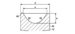
導光柱42は円柱状に形成され、導光柱42の一端側はグローブ15の最大外径部Dの中心に配置され、導光柱42の他端側の端面は発光部34に対向配置されている。
The
導光柱42の一端側の端面の中央領域には凹部44が形成され、この凹部44の内面に反射膜45が形成されている。凹部44は、導光柱42の一端側の端面からの深さが中心において最も深く、その最も深い箇所から導光柱42の一端側の端面までの間が曲面または傾斜面に形成されている。反射膜45は、光を全反射する全反射膜、光の一部を透過するとともに一部を反射する半透過反射膜のいずれでもよい。場合によっては、反射膜45を省略しても良い。本実施形態では、反射膜45として、全反射膜である例えばアルミ蒸着膜が用いられる。なお、凹部44を除く導光柱42の一端側の端面には反射膜45は形成されていない。そのため、この端面に導光した光は導光柱42の一端側に透過して、配光特性を改善することができる。
A
そして、導光柱42の他端側の端面は、発光部34から放射される光が導光柱42に入射する入射面46として構成されている。入射面46から導光柱42に入射した光は、導光柱42内を導光柱42の一端側へ向けて導光される。導光柱42の一端側は、導光柱42内を導光された光を導光柱42の外部に放射する光放射部47として構成されている。光放射部47では、導光柱42内を導光された一部の光が反射膜45で反射して導光柱42の周面や導光柱42の一端側の端面から出射されるとともに、導光柱42内を導光された一部の光が導光柱42の一端側の端面である先端面48から直接出射する。したがって、光放射部47は凹部44および反射膜45が設けられる導光柱42の一端側で構成され、光放射部47からは導光柱42の軸方向に対して交差する横方向、導光柱42の先端方向、導光柱42から筐体11側へ向けた斜め方向を含む広い方向に光が放射される。光放射部47は、グローブ15の最大外径部Dの中心に配置されている。そして、光放射部47から放射される光により、白熱クリア電球が点灯しているような、きらめき感が再現されることができる。
The end surface on the other end side of the
固定部43は、導光柱42の他端側の周面の2箇所から互いに反対方向に向けて突設されている。各固定部43は、導光柱42に連続する連続部49、および連続部49の先端に設けられる突出部50を備えている。連続部49の厚みは突出部50の厚みよりも薄く、連続部49の幅は導光柱42の直径よりも小さく形成されている。
The fixing
突出部50の一端側の面にはカバー14に結合される突起51が突設され、突出部50の他端側の面には基板30の挿通孔39に挿通されて位置決めされる突起52が突設されている。突起52の先端は筐体11の窪み部26に進入し、筐体11とは接触しないように構成されている。そのため、導光体13と基板30とが確実に位置決めされ、これにより、発光部34と導光柱42の入射面46とが位置決めされる。そして、導光体13の固定部43は基板30とカバー14との間に挟み込まれて固定されている。
A
また、カバー14は、絶縁性を有する樹脂材料によって形成されている。カバー14は、中央が一端側に突出する曲面状に形成され、筐体11の一端側、発光モジュール12および導光柱42の他端側を覆う。カバー14の中央には、導光柱42が挿通される挿通孔55が形成されている。カバー14の周辺部には、基板30の他端面の面に引っ掛かる複数の爪56が設けられている。爪56が基板30の他端側の面に引っ掛かることにより、基板30とカバー14との間で導光体13の固定部43を挟持した状態で、カバー14が基板30に固定される。爪56は筐体11の逃げ部27に配置される。カバー14の内面には、固定部の突起51が嵌り込む筒状の保持部57が形成されている。
The
また、グローブ15は、光透過率が95%以上の透明な材料によって形成されている。透明な材料としては、ガラスや樹脂を用いられる。グローブ15は、中空状で、一端側に球面部60が形成され、一端側から他端側にかけて直径が縮径する縮径部61が形成され、他端側が開口されている。グローブ15の他端側には、筐体11の取付溝28に差し込まれて例えばシリコーン接着剤等で接着固定される開口縁62が形成されている。そして、グローブ15の球面部60の最大外径部Dの中心に、光放射部47が配置されている。
The
また、ケース16は、絶縁性を有する樹脂材料によって円筒状に形成されている。ケース16の一端側は筐体11の空洞に挿入され、筐体11の取付孔24を挿通するねじがケース16の一端側に螺着されることによりケース16が筐体11に固定される。ケース16の他端側には給電部18が取り付けられる。ケース16の内側の対向する2箇所には、一対の基板保持部65がランプ軸zに沿って形成されている。
The
また、電源部17は、給電部18から入力する交流電力を所定の直流電力に変換して発光モジュール12の発光素子31に供給する。電源部17は、回路基板68、およびこの回路基板68に実装された複数の電子部品69を有している。回路基板68は、筐体11の一端側から、一対の基板保持部65間に挿入され、筐体11に保持されている。そして、電源部17の交流電力の一対の入力部は配線によって給電部18に電気的に接続され、電源部17の直流電力の一対の出力部は配線によって発光モジュール12のコネクタ35に電気的に接続されている。
Further, the
また、給電部18は、例えばE26やE17等の一般照明白熱電球用のソケットに接続可能な口金が用いられている。なお、給電部18は、口金に限らず、ランプ種類によっては一対のピンでもよい。
In addition, the
なお、ランプ装置10は、ランプ軸zの方向におけるランプ全長に対するグローブ15の領域の割合は、55%以上、望ましくは60%以上である。
In the
そして、本実施形態の作用を説明する。 And the effect | action of this embodiment is demonstrated.
ランプ装置10は、給電部18を照明装置の一般照明用白熱電球用のソケットに接続して使用する。交流電力がソケットを通じてランプ装置10に供給されると、電源部17が交流電力を所定の直流電力に変換して発光素子31に供給する。これにより、発光素子31が発光し、発光部34から光が放射される。
The
発光部34から放射される光は、入射面46から導光柱42に入射し、導光柱42内を光放射部47へ向けて導光される。光放射部47に導光された光は、凹部44の反射膜45で反射して導光柱42の周面や導光柱42の一端側の端面から出射されるとともに、導光柱42の一端側の端面である先端面48から直接出射する。したがって、光放射部47からは、導光柱42の軸方向に対して交差する横方向、導光柱42の先端方向、導光柱42から筐体11側へ向けた斜め方向を含む広い方向に光が放射される。光放射部47から放射された光は、グローブ15を透過し、照明空間に照射される。
The light emitted from the
そして、ランプ装置10は、導光柱42の光放射部47から光を放射することにより、白熱クリア電球が点灯しているような、きらめき感を再現することができる。
The
光放射部47は、グローブ15の最大外径部Dの中心に配置されているため、光放射部47から放射方向に放射される光がグローブ15に垂直に入射してグローブ15を透過しやすく、グローブ15の内面での不要な光の反射が抑制されるため、きらめき感を向上できるとともに、グローブ15外への光取出効率を向上できる。
Since the
なお、ランプ装置10を一般照明用白熱電球に近似した寸法に構成すると、光放射部47をグローブ15の最大外径部Dの中心に配置するのに必要な導光柱42の長さは35〜45mmの範囲にある。
If the
また、導光柱42の直径dは、2〜9mmの範囲にある。導光柱42の直径dが2mmより細いと、発光部34の光が導光柱42に入射しにくく、効率が低下し、また、導光柱42の直径dが9mmよりも太いと、光放射部47が大きくなり、きらめき感が低下する。
Moreover, the diameter d of the
また、図4に示すように、導光柱42の凹部44の開口径(最も広く開口している部分の径)aは、導光柱42の直径dの80〜95%の範囲にある。80%よりも小さいと、導光柱42の横方向や導光柱42から筐体11側へ向けた斜め方向への光が減少し、また、95%よりも大きいと、導光柱42の先端面48の面積が小さくなり、先端面48から出射する光が減少する。ここで、導光柱42の直径dが6mm、凹部44の開口径aが4.9mm、導光柱42の凹部44の開口径aに対する導光柱42の直径dの比率が82%の場合の配光分布を図5に示す。図5から分かるように、配光角は約300゜で、白熱クリア電球と同等の広配光が得られた。なお、この場合の凹部44の深さbは2.1mmであり、凹部44の開口径aに対する凹部44の深さbの比率は43%である。
As shown in FIG. 4, the opening diameter (the diameter of the widest opening portion) a of the
また、図4に示すように、導光柱42の凹部44の深さbは、凹部44の開口径aに対して30〜70%の範囲にある。凹部44の深さbが凹部44の開口径aに対して30〜70%の範囲にあることにより、光放射部47から放射する光を導光柱42の横方向や導光柱42から筐体11側へ向けた斜め方向に反射することができ、白熱クリア電球のようなバランスの良い配光特性を得ることができる。すなわち、凹部44の深さbが凹部44の開口径aに対して30%より小さいと、導光柱42の横方向に反射される光が減少し、また、凹部44の深さbが凹部44の開口径aに対して70%より大きいと、導光柱42から筐体11側へ向けた斜め方向に反射される光が減少する。導光柱42の横方向に反射される光が減少したり、導光柱42から筐体11側へ向けた斜め方向に反射される光が減少することにより、配向分布が偏って、白熱クリア電球のような、きらめき感を再現が難しくなる。
Further, as shown in FIG. 4, the depth b of the
また、図6に示すように、導光柱42の他端側の端面である入射面46の大きさは、発光部34の大きさよりも大きい。そのため、発光部34から放射される光のほとんどを導光柱42に入射させ、漏れ光を少なくすることができ、これにより、光放射部47から放射する光を増加し、きらめき感を向上できる。
In addition, as shown in FIG. 6, the size of the
導光柱42の入射面46と発光部34との間には空気層72が形成されている。空気層72がない場合、すなわち、入射面46と発光部34とが密着している場合、発光部34から導光柱42に入射した光の一部が導光柱42の一端側に導光されずに導光柱42の周面から出射されやすくなる。空気層72がある場合、発光部34から放射された光が空気層72を通じて導光柱42に入射する際に屈折が生じ、屈折した光が光放射部47へ向けて導光柱42内を導光される。
An
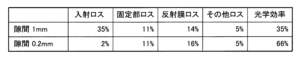
導光柱42の入射面46と発光部34との間には空気層72の隙間は、効率に大きな影響を及ぼす。図7に示すように、空気層72の隙間が広いと、発光部34から入射面46への入射ロスが大きくなり、効率が低下する。なお、ロスの比較例として、導光体13の固定部43でのロス、反射膜45でのロス、その他のロスを示すが、空気層72の隙間が効率に大きな影響を及ぼすことが分かる。そのため、空気層72の隙間をできるだけ少なくなるように、導光柱42と発光部34をできるだけ近付けることが好ましい。ところで、導光柱42を発光部34に近付けることにより、導光柱42が発光部34に接触し、発光部34に影響を及ぼすおそれがある。本実施形態では、発光部34である蛍光体層33の表面は、枠部32よりも窪んでいるため、導光柱42が枠部32に当接しても、導光柱42が蛍光体層33に接触することがない。そのため、導光柱42と発光部34をできるだけ近付けながら、発光部34に影響を及ぼすのを防止できる。
The gap of the
また、導光体13の固定部43は、導光柱42の他端側の周面の2箇所から突出されている。入射面46から導光柱42に入射した光の一部は、導光柱42に接続されている固定部43に漏れ、効率が低下する。導光体13の固定部43を導光柱42の他端側の周面の2箇所から突出していることにより、例えば、導光柱42の他端側の周面全体から固定部分が突出されている場合に比べて、漏れ光が少なくすることができ、これにより、光放射部47から放射する光を増加し、きらめき感を向上できる。
Further, the fixing
しかも、固定部43は、導光柱42に連続する連続部49、および連続部49の先端に設けられる突出部50を備えているが、連続部49の厚みを突出部50の厚みよりも薄く、連続部49の幅を導光柱42の直径よりも小さくしているため、導光体13を筐体11に固定するための固定部43の強度を確保しながら、固定部43への漏れ光を少なくすることができる。
Moreover, the fixed
また、カバー14により、発光部34および導光柱42の他端側を覆うため、筐体11の近傍から光が放射されるのを防止し、光放射部47のみから光が放射されるようにして、きらめき感を向上できる。
Further, since the
次に、きらめき感について説明する。 Next, the glittering feeling will be described.
きらめき感とは「光が美しく光っているように見えること」という意味で用いられている。 The sense of glitter is used to mean that the light appears to shine beautifully.
ここで、きらめき感がある光源とは、「平均輝度が5000cd/m2(好ましくは45000cd/m2)以上でかつ光源(光放射部47)から10m離れたときの見かけの大きさが0.000001sr以下である光源」、もしくは、「平均輝度が5000cd/m2(好ましくは45000cd/m2)以上でかつ大きさが64mm2(好ましくは17mm2)以下である光源」と定義した。なお、好ましくとしている数値に設定すると、白熱クリア電球以上のきらめき感が得られる可能性が高い。その理由を(1)(2)に示す。 Here, the light source there is a sense of glitter, is apparent sizes when "the average luminance is 5000 cd / m 2 (preferably 45000cd / m 2) away 10m from or more and a light source (light emitting portion 47) 0. Defined as “a light source having an average luminance of 5000 cd / m 2 (preferably 45000 cd / m 2 ) or more and a size of 64 mm 2 (preferably 17 mm 2 )” or less. In addition, if it sets to the preferable numerical value, possibility that the glittering feeling more than an incandescent clear light bulb will be acquired is high. The reasons are shown in (1) and (2).
(1)白熱クリア電球は店舗などの雰囲気重視の場面で使用されると、きらめき感があると言われているが、オフィスなどの作業重視の場面で使用されると、非常にまぶしいと言われている。そこで、きらめき感が得られる輝度=まぶしさを感じる輝度として、光源の輝度条件を設定した。 (1) Incandescent clear light bulbs are said to have a sparkle when used in atmosphere-oriented scenes such as in stores, but they are said to be very dazzling when used in office-oriented situations. ing. Therefore, the luminance condition of the light source was set as the luminance at which glittering feeling can be obtained = luminance at which glare is felt.
直視でのまぶしさを数値化する式1を用いて算出した結果、まぶしさを感じる平均輝度は5000cd/m2(nUGRD=13のとき、図8参照)、確実にまぶしく感じる平均輝度は45000cd/m2(nUGRD=31のとき、図8参照)となった。そのため、平均輝度の条件を5000cd/m2、好ましくは45000cd/m2とした。 As a result of calculation using Expression 1 for quantifying the glare in direct viewing, the average brightness that feels glare is 5000 cd / m 2 (refer to FIG. 8 when nUGR D = 13), and the average brightness that feels brightly is 45000 cd. / M 2 (when nUGR D = 31, refer to FIG. 8). Therefore, conditions 5000 cd / m 2 in average luminance, preferably has a 45000cd / m 2.
なお、これらの平均輝度はランプ装置10の有効な配光角度(本実施形態の場合、図5で示す300°)の範囲内における測定結果により定義することが可能である。 Note that these average luminances can be defined by measurement results within a range of an effective light distribution angle of the lamp device 10 (in the present embodiment, 300 ° shown in FIG. 5).
光源の平均輝度LS、背景の平均輝度(光源周辺の平均輝度)Lb、光源の大きさω、光源の輝度分布(平均輝度/最大輝度)U、まぶしさの程度(図8参照)nUGRDである。また、算出条件:Lb=30cd/m2、ω=0.000001sr、U=1.0である。 Average luminance L S of the light source, average luminance of the background (average luminance around the light source) L b , size of the light source ω, luminance distribution of the light source (average luminance / maximum luminance) U, degree of glare (see FIG. 8) nUGR D. In addition, the calculation conditions are L b = 30 cd / m 2 , ω = 0.0001 sr, and U = 1.0.
図9に示すように、光源の平均輝度が5000cd/m2以上の領域A1できらめき感が得られ、光源の平均輝度が45000cd/m2以上の領域A2で白熱クリア電球以上のきらめき感が得られる。 As shown in FIG. 9, the average luminance of the light source is obtained feeling sparkle at 5000 cd / m 2 or more regions A1, resulting feeling glitter or more incandescent clear bulb average luminance of the light source in 45000cd / m 2 or more regions A2 It is done.
(2)光源を直視すると光芒(放射上に広がる光の線)が見られ、光の線が細い光芒ほど、きらめき感がある光源と言われている。 (2) When looking directly at the light source, a light beam (a line of light spreading on the radiation) is seen, and a light beam with a narrower light line is said to be a light source with a glittering feeling.
光芒は光源が小さいほど放射状に広がる光の線が細くなるため、光源を所定の大きさよりも小さくすれば、きらめき感がある光源を実現することができる。そのため、ここではその所定の大きさを以下のように定めた。 Since the light beam spreads radially as the light source is smaller, a light source with a glittering feeling can be realized by making the light source smaller than a predetermined size. Therefore, the predetermined size is determined here as follows.
一般的に、きらめき感がある光源と言われている白熱クリア電球の光源を10m離れた距離から観察した見かけの大きさをきらめき感が得られる光源の見かけの大きさとした。その大きさは「0.000001sr以下」である。以下、これを基準の見かけの大きさと呼ぶ。 In general, the apparent size of an incandescent clear light bulb, which is said to be a light source with glitter, is observed from a distance of 10 m. Its size is “0.000001 sr or less”. Hereinafter, this is referred to as a reference apparent size.
そして、実際の光源の大きさは10m離れた距離から光源を観察したときに、基準の見かけの大きさになるように設定した。その実際の光源の大きさは、64mm2である。なお、64mm2の光源は、円形・球形であれば直径9mm、正方形・立方体であれば1辺の長さは8mmとなる。なお、ここで述べている大きさとは、視線方向に対して垂直な面の大きさである(図12参照)。 The actual size of the light source was set so as to be the reference apparent size when the light source was observed from a distance of 10 m. The actual size of the light source is 64 mm 2 . Note that a 64 mm 2 light source has a diameter of 9 mm if it is circular or spherical, and a side of 8 mm if it is square or cubic. The size described here is the size of a surface perpendicular to the line-of-sight direction (see FIG. 12).
また、実際の光源の大きさを5m離れた距離から光源を観察したときの見かけの大きさが0.000001sr以下とすることが好ましい。その際の実際の光源の大きさが17mm2である。なお、大きさが17mm2の光源は、円形・球形であれば直径4.6mm、正方形・立方体であれば1辺の長さは4.1mmとなる。 Moreover, it is preferable that the apparent size when the size of the actual light source is observed from a distance of 5 m is 0.000001 sr or less. In this case, the actual light source size is 17 mm 2 . A light source having a size of 17 mm 2 has a diameter of 4.6 mm if it is circular or spherical, and has a side length of 4.1 mm if it is square or cubic.
なお、視野角によって光源の見かけの大きさが変化する場合には、その最大の大きさとなる角度によって定義すればよい。本実施形態の場合、図5に示す0°のときが最も見かけの面積が大きく、照度(光束)も大きいが、水平(±90°)のときに、これらが最大値となる形態であってもよい。 In addition, what is necessary is just to define by the angle used as the maximum magnitude | size, when the apparent magnitude | size of a light source changes with viewing angles. In the case of the present embodiment, the apparent area is the largest at 0 ° shown in FIG. 5 and the illuminance (light flux) is also large, but these are the maximum values when horizontal (± 90 °). Also good.
図10に示すように、光源の大きさが64mm2以下の領域A3できらめき感が得られ、光源の大きさが17mm2以下の領域A4で白熱クリア電球以上のきらめき感が得られる。 As shown in FIG. 10, a glittering feeling is obtained in the area A3 where the size of the light source is 64 mm 2 or less, and a glittering feeling more than that of the incandescent clear bulb is obtained in the area A4 where the size of the light source is 17 mm 2 or less.
そして、本実施形態のランプ装置10の光放射部47は、「平均輝度が5000cd/m2(好ましくは45000cd/m2)以上でかつ見かけの大きさが0.000001sr以下である光源」、もしくは、「平均輝度が5000cd/m2(好ましくは45000cd/m2)以上でかつ大きさが64mm2(好ましくは17mm2)以下である光源」の定義に合致している。
The
なお、比較例よりもきらめき感を多く感じさせるためには、光源の大きさを30mm2以下とするのが好ましい。比較例とは、複数の発光素子を備えた発光モジュールをグローブの内部空間に配置したランプ装置である。 It should be noted that the size of the light source is preferably 30 mm 2 or less in order to feel more glitter than the comparative example. The comparative example is a lamp device in which a light emitting module including a plurality of light emitting elements is arranged in an inner space of a globe.
図11は、光源の大きさと光源の輝度との関係の最も好ましい範囲を示したグラフである。図11で示す範囲は、比較例よりもきらめき感を際立たせるとともに、光源(光放出部47)の製造性も比較的容易な光源の大きさを示しており、この望ましい光源の大きさの範囲9〜17mm2である。このグラフにおいて、光源の大きさが17mm2のときには平均輝度は45000cd/m2以上、光源の大きさが9mm2のときには平均輝度は77000cd/m2以上にするときらめき感が際立つ。また、光源の大きさが17mm2のときに平均輝度が2800000cd/m2となると、白熱電球のようなまぶしさを感じるため、これ以下にする必要があり、光源の大きさが9mm2のときには平均輝度4800000cd/m2以下とするのが好ましい。 FIG. 11 is a graph showing the most preferable range of the relationship between the size of the light source and the luminance of the light source. The range shown in FIG. 11 shows the size of the light source that makes the glittering feeling stand out more than the comparative example, and the manufacturability of the light source (light emitting portion 47) is relatively easy. 9 to 17 mm 2 . In this graph, when the size of the light source is 17 mm 2 , the average luminance is 45000 cd / m 2 or more, and when the size of the light source is 9 mm 2 , the glittering feeling is conspicuous when the average luminance is 77000 cd / m 2 or more. Further, when the average luminance is 2800000 cd / m 2 when the size of the light source is 17 mm 2 , it is necessary to make it less than this because it feels glare like an incandescent bulb. When the size of the light source is 9 mm 2 , The average luminance is preferably 480,000 cd / m 2 or less.
実際の光源の大きさと平均輝度との関係を図13に示す。図13中の●は白熱クリア電球、○は比較例、◎は実施形態のランプ装置10である。図13から分かるように、本実施形態のランプ装置10は、比較例と比較して、きらめき感が得られる領域A4に入っている。また、白熱クリア電球と比較しても、同等以上にきらめき感が得られる領域A4に入っている。
FIG. 13 shows the relationship between the actual light source size and average luminance. In FIG. 13, ● is an incandescent clear light bulb, ○ is a comparative example, and ◎ is the
この結果を受け、実際に実施形態のランプ装置10を試作して、十数人の被験者にこれら3つの光源について、どれが最もきらめき感があるかと質問したところ、8〜9割以上の被験者から実施形態のランプ装置10が最もきらめき感があるという回答が得られた。
In response to this result, the prototype of the
このように、光源(光放射部47)の平均輝度および大きさを所定の範囲に入るように設計をすることで、白熱クリア電球と同等以上のきらめき感が得られるランプ装置10を実現することができる。
As described above, by designing the light source (light radiating unit 47) so that the average luminance and size of the light source (light emitting portion 47) are within a predetermined range, the
なお、「平均輝度が5000cd/m2(好ましくは45000cd/m2)以上でかつ見かけの大きさが0.000001sr以下である光源」、もしくは、「平均輝度が5000cd/m2(好ましくは45000cd/m2)以上でかつ大きさが64mm2(好ましくは17mm2)以下である光源」の定義に合致していれば、光源は、平面光源でも立体光源(球形、立方体、直方体、柱体、角錐体等)等でもよい。いずれの光源も、グローブ15の先端方向および筐体11の方向に光を放出可能であればよい。
Note that “a light source having an average luminance of 5000 cd / m 2 (preferably 45000 cd / m 2 ) or more and an apparent size of 0.000001 sr or less” or “an average luminance of 5000 cd / m 2 (preferably 45000 cd / m). m 2 ) and a size of 64 mm 2 (preferably 17 mm 2 ) or less ”, the light source can be a planar light source or a solid light source (spherical, cube, rectangular parallelepiped, column, pyramid) Body etc.). Any light source may be used as long as light can be emitted in the direction of the tip of the
本発明のいくつかの実施形態を説明したが、これらの実施形態は、例として提示したものであり、発明の範囲を限定することは意図していない。これら新規な実施形態は、その他の様々な形態で実施されることが可能であり、発明の要旨を逸脱しない範囲で、種々の省略、置き換え、変更を行うことができる。これら実施形態やその変形は、発明の範囲や要旨に含まれるとともに、特許請求の範囲に記載された発明とその均等の範囲に含まれる。 Although several embodiments of the present invention have been described, these embodiments are presented by way of example and are not intended to limit the scope of the invention. These novel embodiments can be implemented in various other forms, and various omissions, replacements, and changes can be made without departing from the scope of the invention. These embodiments and modifications thereof are included in the scope and gist of the invention, and are included in the invention described in the claims and the equivalents thereof.
10 ランプ装置
11 筐体
12 発光モジュール
13 導光体
14 カバー
15 グローブ
18 給電部
30 基板
31 発光素子
32 枠部
33 蛍光体層
34 発光部
42 導光柱
43 固定部
44 凹部
55 挿通孔
10 Lamp device
11 Enclosure
12 light emitting module
13 Light guide
14 Cover
15 Globe
18 Feeding unit
30 substrates
31 Light emitting element
32 Frame
33 Phosphor layer
34 Light emitter
42 Light guide column
43 Fixed part
44 recess
55 Insertion hole
Claims (5)
前記筐体の一端側に配置される発光部を有する発光モジュールと;
前記発光部を覆って前記筐体の一端側に配置される透明なグローブと;
導光柱を有し、この導光柱の一端側が前記グローブの最大外径部の中心に配置され、前記導光柱の他端側の端面が前記発光部に対向配置され、前記導光柱の一端側の端面に光の向きを変える機能を有する導光体と;
前記筐体の他端側に配置される給電部と;
を具備し、
前記発光部の大きさは、前記導光柱の他端側の端面の大きさよりも小さく、
前記発光モジュールは、基板、この基板に実装された複数の発光素子、これら発光素子の周囲を囲む枠部、およびこの枠部内に前記発光素子を覆うように充填され表面が前記発光部として構成される蛍光体層を有し、前記蛍光体層の表面は前記枠部よりも窪んでいる
ことを特徴とするランプ装置。 A housing;
A light emitting module having a light emitting portion disposed on one end side of the housing;
A transparent glove that covers the light emitting portion and is disposed on one end side of the housing;
Has a light guide posts, one end side of the light guide pillar is placed in the center of the maximum outer diameter of the globe, and the other end face of the light guide pillar is arranged opposite to the light emitting portion, the one end side of the light guide pillar A light guide having a function of changing the direction of light on the end face;
A power feeding unit disposed on the other end of the housing;
Equipped with,
The size of the light emitting portion is smaller than the size of the end face on the other end side of the light guide column,
The light emitting module includes a substrate, a plurality of light emitting elements mounted on the substrate, a frame portion surrounding the light emitting elements, and a surface filled with the light emitting element so as to cover the light emitting elements. And a surface of the phosphor layer is recessed from the frame portion .
前記凹部の開口径は、前記導光柱の直径の80〜95%の範囲にある
ことを特徴とする請求項1記載のランプ装置。 The function of changing the direction of the light of the light guide is a recess formed on the end surface on one end side of the light guide column,
The lamp device according to claim 1, wherein an opening diameter of the concave portion is in a range of 80 to 95% of a diameter of the light guide column.
ことを特徴とする請求項2記載のランプ装置。 The depth of the said recessed part exists in the range of 30 to 70% with respect to the opening diameter of the said recessed part. The lamp device of Claim 2 characterized by the above-mentioned.
ことを特徴とする請求項1ないし3いずれか一記載のランプ装置。 The said light guide is protruded from two places of the surrounding surface of the other end side of the said light guide pillar, and has the fixing | fixed part fixed to the said housing | casing. Lamp device.
ことを特徴とする請求項1ないし4いずれか一記載のランプ装置。 The insertion hole which the said light guide column penetrates is formed, The cover which covers the one end side of the said housing | casing, the said light emission part, and the other end side of the said light guide column is comprised. The lamp device according to one .
Priority Applications (2)
| Application Number | Priority Date | Filing Date | Title |
|---|---|---|---|
| JP2014233058A JP6410033B2 (en) | 2014-11-17 | 2014-11-17 | Lamp device |
| CN201520696616.7U CN204922595U (en) | 2014-11-17 | 2015-09-09 | Lamp device |
Applications Claiming Priority (1)
| Application Number | Priority Date | Filing Date | Title |
|---|---|---|---|
| JP2014233058A JP6410033B2 (en) | 2014-11-17 | 2014-11-17 | Lamp device |
Publications (2)
| Publication Number | Publication Date |
|---|---|
| JP2016096120A JP2016096120A (en) | 2016-05-26 |
| JP6410033B2 true JP6410033B2 (en) | 2018-10-24 |
Family
ID=54971720
Family Applications (1)
| Application Number | Title | Priority Date | Filing Date |
|---|---|---|---|
| JP2014233058A Active JP6410033B2 (en) | 2014-11-17 | 2014-11-17 | Lamp device |
Country Status (2)
| Country | Link |
|---|---|
| JP (1) | JP6410033B2 (en) |
| CN (1) | CN204922595U (en) |
Families Citing this family (3)
| Publication number | Priority date | Publication date | Assignee | Title |
|---|---|---|---|---|
| JP7004148B2 (en) * | 2017-12-05 | 2022-02-04 | 東芝ライテック株式会社 | Optical assembly, lamps and lighting |
| JP2021072187A (en) * | 2019-10-30 | 2021-05-06 | パナソニックIpマネジメント株式会社 | Lens, luminaire, and illuminating system |
| WO2023094324A1 (en) * | 2021-11-25 | 2023-06-01 | Signify Holding B.V. | Lightguide lamp |
Family Cites Families (4)
| Publication number | Priority date | Publication date | Assignee | Title |
|---|---|---|---|---|
| US6350041B1 (en) * | 1999-12-03 | 2002-02-26 | Cree Lighting Company | High output radial dispersing lamp using a solid state light source |
| KR101839417B1 (en) * | 2009-01-09 | 2018-03-16 | 필립스 라이팅 홀딩 비.브이. | Light source with leds, light guide and reflector |
| JP5668251B2 (en) * | 2010-08-31 | 2015-02-12 | 東芝ライテック株式会社 | Light bulb shaped lamp and lighting equipment |
| JP2013200963A (en) * | 2012-03-23 | 2013-10-03 | Harison Toshiba Lighting Corp | Semiconductor light source, and lighting device |
-
2014
- 2014-11-17 JP JP2014233058A patent/JP6410033B2/en active Active
-
2015
- 2015-09-09 CN CN201520696616.7U patent/CN204922595U/en active Active
Also Published As
| Publication number | Publication date |
|---|---|
| JP2016096120A (en) | 2016-05-26 |
| CN204922595U (en) | 2015-12-30 |
Similar Documents
| Publication | Publication Date | Title |
|---|---|---|
| JP5320609B2 (en) | Lamp apparatus and lighting apparatus | |
| US20130308319A1 (en) | Led lamp | |
| JP5575715B2 (en) | Light bulb type lighting device | |
| JP6410033B2 (en) | Lamp device | |
| JP6521226B2 (en) | Lamp device | |
| JP6497501B2 (en) | Light emitting device | |
| JP2017208206A (en) | Luminaire | |
| JP6241611B2 (en) | Lamp device and lighting device | |
| JP6540953B2 (en) | Lamp device | |
| JP2017033804A (en) | Lighting fixture | |
| JP6700573B2 (en) | Lamp device | |
| JP6642799B2 (en) | Lamp device | |
| JP2017073271A (en) | Lamp device | |
| JP2017010667A (en) | Lamp device | |
| JP2016219326A (en) | Lamp device | |
| JP7004148B2 (en) | Optical assembly, lamps and lighting | |
| JP7144736B2 (en) | lamp system and lighting system | |
| JP2014146570A (en) | Lamp and illumination device | |
| JP6979161B2 (en) | Lamps and lighting | |
| JP2019003834A (en) | Luminaire | |
| JP2017062935A (en) | Lamp device | |
| JPWO2012153442A1 (en) | Light source for illumination | |
| JP2018045953A (en) | Lamp device and lighting device | |
| JP2017174778A (en) | Lamp apparatus | |
| JP2018055826A (en) | Lamp device and luminaire |
Legal Events
| Date | Code | Title | Description |
|---|---|---|---|
| A621 | Written request for application examination |
Free format text: JAPANESE INTERMEDIATE CODE: A621 Effective date: 20170912 |
|
| A131 | Notification of reasons for refusal |
Free format text: JAPANESE INTERMEDIATE CODE: A131 Effective date: 20180523 |
|
| A977 | Report on retrieval |
Free format text: JAPANESE INTERMEDIATE CODE: A971007 Effective date: 20180525 |
|
| A521 | Written amendment |
Free format text: JAPANESE INTERMEDIATE CODE: A523 Effective date: 20180711 |
|
| TRDD | Decision of grant or rejection written | ||
| A01 | Written decision to grant a patent or to grant a registration (utility model) |
Free format text: JAPANESE INTERMEDIATE CODE: A01 Effective date: 20180829 |
|
| A61 | First payment of annual fees (during grant procedure) |
Free format text: JAPANESE INTERMEDIATE CODE: A61 Effective date: 20180911 |
|
| R151 | Written notification of patent or utility model registration |
Ref document number: 6410033 Country of ref document: JP Free format text: JAPANESE INTERMEDIATE CODE: R151 |