JP6376574B2 - Non-planar transistors, systems, and methods of manufacturing non-planar transistors including microelectronic device isolation produced by the formation of catalytic oxides - Google Patents
Non-planar transistors, systems, and methods of manufacturing non-planar transistors including microelectronic device isolation produced by the formation of catalytic oxides Download PDFInfo
- Publication number
- JP6376574B2 JP6376574B2 JP2017505089A JP2017505089A JP6376574B2 JP 6376574 B2 JP6376574 B2 JP 6376574B2 JP 2017505089 A JP2017505089 A JP 2017505089A JP 2017505089 A JP2017505089 A JP 2017505089A JP 6376574 B2 JP6376574 B2 JP 6376574B2
- Authority
- JP
- Japan
- Prior art keywords
- fin
- transistor
- oxide
- type channel
- semiconductor body
- Prior art date
- Legal status (The legal status is an assumption and is not a legal conclusion. Google has not performed a legal analysis and makes no representation as to the accuracy of the status listed.)
- Active
Links
- 238000000034 method Methods 0.000 title claims description 41
- 238000002955 isolation Methods 0.000 title claims description 28
- 238000004377 microelectronic Methods 0.000 title claims description 15
- 238000004519 manufacturing process Methods 0.000 title claims description 7
- 230000003197 catalytic effect Effects 0.000 title claims description 3
- 230000015572 biosynthetic process Effects 0.000 title description 10
- 239000004065 semiconductor Substances 0.000 claims description 139
- 230000003647 oxidation Effects 0.000 claims description 62
- 238000007254 oxidation reaction Methods 0.000 claims description 62
- 239000003054 catalyst Substances 0.000 claims description 55
- 238000000926 separation method Methods 0.000 claims description 24
- 239000000463 material Substances 0.000 claims description 23
- XUIMIQQOPSSXEZ-UHFFFAOYSA-N Silicon Chemical compound [Si] XUIMIQQOPSSXEZ-UHFFFAOYSA-N 0.000 claims description 22
- 229910052710 silicon Inorganic materials 0.000 claims description 22
- 239000010703 silicon Substances 0.000 claims description 22
- TWNQGVIAIRXVLR-UHFFFAOYSA-N oxo(oxoalumanyloxy)alumane Chemical compound O=[Al]O[Al]=O TWNQGVIAIRXVLR-UHFFFAOYSA-N 0.000 claims description 16
- VYPSYNLAJGMNEJ-UHFFFAOYSA-N Silicium dioxide Chemical compound O=[Si]=O VYPSYNLAJGMNEJ-UHFFFAOYSA-N 0.000 claims description 15
- 238000000059 patterning Methods 0.000 claims description 14
- GWEVSGVZZGPLCZ-UHFFFAOYSA-N Titan oxide Chemical compound O=[Ti]=O GWEVSGVZZGPLCZ-UHFFFAOYSA-N 0.000 claims description 11
- 229910052782 aluminium Inorganic materials 0.000 claims description 11
- XAGFODPZIPBFFR-UHFFFAOYSA-N aluminium Chemical compound [Al] XAGFODPZIPBFFR-UHFFFAOYSA-N 0.000 claims description 11
- 229910000449 hafnium oxide Inorganic materials 0.000 claims description 11
- WIHZLLGSGQNAGK-UHFFFAOYSA-N hafnium(4+);oxygen(2-) Chemical compound [O-2].[O-2].[Hf+4] WIHZLLGSGQNAGK-UHFFFAOYSA-N 0.000 claims description 11
- SIWVEOZUMHYXCS-UHFFFAOYSA-N oxo(oxoyttriooxy)yttrium Chemical compound O=[Y]O[Y]=O SIWVEOZUMHYXCS-UHFFFAOYSA-N 0.000 claims description 11
- BPUBBGLMJRNUCC-UHFFFAOYSA-N oxygen(2-);tantalum(5+) Chemical compound [O-2].[O-2].[O-2].[O-2].[O-2].[Ta+5].[Ta+5] BPUBBGLMJRNUCC-UHFFFAOYSA-N 0.000 claims description 11
- RVTZCBVAJQQJTK-UHFFFAOYSA-N oxygen(2-);zirconium(4+) Chemical compound [O-2].[O-2].[Zr+4] RVTZCBVAJQQJTK-UHFFFAOYSA-N 0.000 claims description 11
- 229910001936 tantalum oxide Inorganic materials 0.000 claims description 11
- OGIDPMRJRNCKJF-UHFFFAOYSA-N titanium oxide Inorganic materials [Ti]=O OGIDPMRJRNCKJF-UHFFFAOYSA-N 0.000 claims description 11
- 229910001928 zirconium oxide Inorganic materials 0.000 claims description 11
- 230000001590 oxidative effect Effects 0.000 claims description 9
- 235000012239 silicon dioxide Nutrition 0.000 claims description 7
- 239000000377 silicon dioxide Substances 0.000 claims description 7
- GQPLMRYTRLFLPF-UHFFFAOYSA-N Nitrous Oxide Chemical compound [O-][N+]#N GQPLMRYTRLFLPF-UHFFFAOYSA-N 0.000 claims description 6
- 239000007789 gas Substances 0.000 claims description 4
- 239000000203 mixture Substances 0.000 claims description 4
- 239000001272 nitrous oxide Substances 0.000 claims description 3
- QVGXLLKOCUKJST-UHFFFAOYSA-N atomic oxygen Chemical compound [O] QVGXLLKOCUKJST-UHFFFAOYSA-N 0.000 claims description 2
- 239000001257 hydrogen Substances 0.000 claims description 2
- 229910052739 hydrogen Inorganic materials 0.000 claims description 2
- 239000001301 oxygen Substances 0.000 claims description 2
- 229910052760 oxygen Inorganic materials 0.000 claims description 2
- 125000004435 hydrogen atom Chemical class [H]* 0.000 claims 1
- 239000000758 substrate Substances 0.000 description 14
- 238000004891 communication Methods 0.000 description 13
- 239000007772 electrode material Substances 0.000 description 5
- 238000005530 etching Methods 0.000 description 5
- 238000000231 atomic layer deposition Methods 0.000 description 4
- 229910052751 metal Inorganic materials 0.000 description 3
- 239000002184 metal Substances 0.000 description 3
- 238000000206 photolithography Methods 0.000 description 3
- PXHVJJICTQNCMI-UHFFFAOYSA-N Nickel Chemical compound [Ni] PXHVJJICTQNCMI-UHFFFAOYSA-N 0.000 description 2
- KDLHZDBZIXYQEI-UHFFFAOYSA-N Palladium Chemical compound [Pd] KDLHZDBZIXYQEI-UHFFFAOYSA-N 0.000 description 2
- 229910004298 SiO 2 Inorganic materials 0.000 description 2
- 239000013078 crystal Substances 0.000 description 2
- 239000003989 dielectric material Substances 0.000 description 2
- 230000006870 function Effects 0.000 description 2
- MRELNEQAGSRDBK-UHFFFAOYSA-N lanthanum(3+);oxygen(2-) Chemical compound [O-2].[O-2].[O-2].[La+3].[La+3] MRELNEQAGSRDBK-UHFFFAOYSA-N 0.000 description 2
- 229910021421 monocrystalline silicon Inorganic materials 0.000 description 2
- 238000005240 physical vapour deposition Methods 0.000 description 2
- BASFCYQUMIYNBI-UHFFFAOYSA-N platinum Chemical compound [Pt] BASFCYQUMIYNBI-UHFFFAOYSA-N 0.000 description 2
- 229910052715 tantalum Inorganic materials 0.000 description 2
- GUVRBAGPIYLISA-UHFFFAOYSA-N tantalum atom Chemical compound [Ta] GUVRBAGPIYLISA-UHFFFAOYSA-N 0.000 description 2
- JBRZTFJDHDCESZ-UHFFFAOYSA-N AsGa Chemical compound [As]#[Ga] JBRZTFJDHDCESZ-UHFFFAOYSA-N 0.000 description 1
- MYMOFIZGZYHOMD-UHFFFAOYSA-N Dioxygen Chemical compound O=O MYMOFIZGZYHOMD-UHFFFAOYSA-N 0.000 description 1
- 229910001218 Gallium arsenide Inorganic materials 0.000 description 1
- UFHFLCQGNIYNRP-UHFFFAOYSA-N Hydrogen Chemical compound [H][H] UFHFLCQGNIYNRP-UHFFFAOYSA-N 0.000 description 1
- 229910000673 Indium arsenide Inorganic materials 0.000 description 1
- GPXJNWSHGFTCBW-UHFFFAOYSA-N Indium phosphide Chemical compound [In]#P GPXJNWSHGFTCBW-UHFFFAOYSA-N 0.000 description 1
- KJTLSVCANCCWHF-UHFFFAOYSA-N Ruthenium Chemical compound [Ru] KJTLSVCANCCWHF-UHFFFAOYSA-N 0.000 description 1
- 229910052581 Si3N4 Inorganic materials 0.000 description 1
- RTAQQCXQSZGOHL-UHFFFAOYSA-N Titanium Chemical compound [Ti] RTAQQCXQSZGOHL-UHFFFAOYSA-N 0.000 description 1
- QCWXUUIWCKQGHC-UHFFFAOYSA-N Zirconium Chemical compound [Zr] QCWXUUIWCKQGHC-UHFFFAOYSA-N 0.000 description 1
- 229910026551 ZrC Inorganic materials 0.000 description 1
- OTCHGXYCWNXDOA-UHFFFAOYSA-N [C].[Zr] Chemical compound [C].[Zr] OTCHGXYCWNXDOA-UHFFFAOYSA-N 0.000 description 1
- XWCMFHPRATWWFO-UHFFFAOYSA-N [O-2].[Ta+5].[Sc+3].[O-2].[O-2].[O-2] Chemical compound [O-2].[Ta+5].[Sc+3].[O-2].[O-2].[O-2] XWCMFHPRATWWFO-UHFFFAOYSA-N 0.000 description 1
- ILCYGSITMBHYNK-UHFFFAOYSA-N [Si]=O.[Hf] Chemical compound [Si]=O.[Hf] ILCYGSITMBHYNK-UHFFFAOYSA-N 0.000 description 1
- CAVCGVPGBKGDTG-UHFFFAOYSA-N alumanylidynemethyl(alumanylidynemethylalumanylidenemethylidene)alumane Chemical compound [Al]#C[Al]=C=[Al]C#[Al] CAVCGVPGBKGDTG-UHFFFAOYSA-N 0.000 description 1
- VKJLWXGJGDEGSO-UHFFFAOYSA-N barium(2+);oxygen(2-);titanium(4+) Chemical compound [O-2].[O-2].[O-2].[Ti+4].[Ba+2] VKJLWXGJGDEGSO-UHFFFAOYSA-N 0.000 description 1
- 238000005229 chemical vapour deposition Methods 0.000 description 1
- 229910017052 cobalt Inorganic materials 0.000 description 1
- 239000010941 cobalt Substances 0.000 description 1
- GUTLYIVDDKVIGB-UHFFFAOYSA-N cobalt atom Chemical compound [Co] GUTLYIVDDKVIGB-UHFFFAOYSA-N 0.000 description 1
- 238000007796 conventional method Methods 0.000 description 1
- 230000003247 decreasing effect Effects 0.000 description 1
- 238000000151 deposition Methods 0.000 description 1
- 238000013461 design Methods 0.000 description 1
- 238000011161 development Methods 0.000 description 1
- 229910001882 dioxygen Inorganic materials 0.000 description 1
- 238000001312 dry etching Methods 0.000 description 1
- 239000012777 electrically insulating material Substances 0.000 description 1
- 230000005670 electromagnetic radiation Effects 0.000 description 1
- VTGARNNDLOTBET-UHFFFAOYSA-N gallium antimonide Chemical compound [Sb]#[Ga] VTGARNNDLOTBET-UHFFFAOYSA-N 0.000 description 1
- 229910052732 germanium Inorganic materials 0.000 description 1
- GNPVGFCGXDBREM-UHFFFAOYSA-N germanium atom Chemical compound [Ge] GNPVGFCGXDBREM-UHFFFAOYSA-N 0.000 description 1
- 229910052735 hafnium Inorganic materials 0.000 description 1
- VBJZVLUMGGDVMO-UHFFFAOYSA-N hafnium atom Chemical compound [Hf] VBJZVLUMGGDVMO-UHFFFAOYSA-N 0.000 description 1
- WHJFNYXPKGDKBB-UHFFFAOYSA-N hafnium;methane Chemical compound C.[Hf] WHJFNYXPKGDKBB-UHFFFAOYSA-N 0.000 description 1
- 150000002431 hydrogen Chemical class 0.000 description 1
- WPYVAWXEWQSOGY-UHFFFAOYSA-N indium antimonide Chemical compound [Sb]#[In] WPYVAWXEWQSOGY-UHFFFAOYSA-N 0.000 description 1
- RPQDHPTXJYYUPQ-UHFFFAOYSA-N indium arsenide Chemical compound [In]#[As] RPQDHPTXJYYUPQ-UHFFFAOYSA-N 0.000 description 1
- 239000012212 insulator Substances 0.000 description 1
- JQJCSZOEVBFDKO-UHFFFAOYSA-N lead zinc Chemical compound [Zn].[Pb] JQJCSZOEVBFDKO-UHFFFAOYSA-N 0.000 description 1
- 230000007774 longterm Effects 0.000 description 1
- 150000001247 metal acetylides Chemical class 0.000 description 1
- 229910044991 metal oxide Inorganic materials 0.000 description 1
- 150000004706 metal oxides Chemical class 0.000 description 1
- 150000002739 metals Chemical class 0.000 description 1
- 229910052759 nickel Inorganic materials 0.000 description 1
- 150000004767 nitrides Chemical class 0.000 description 1
- KJXBRHIPHIVJCS-UHFFFAOYSA-N oxo(oxoalumanyloxy)lanthanum Chemical compound O=[Al]O[La]=O KJXBRHIPHIVJCS-UHFFFAOYSA-N 0.000 description 1
- 238000004806 packaging method and process Methods 0.000 description 1
- 229910052763 palladium Inorganic materials 0.000 description 1
- 229910052697 platinum Inorganic materials 0.000 description 1
- 229910021420 polycrystalline silicon Inorganic materials 0.000 description 1
- 229920005591 polysilicon Polymers 0.000 description 1
- 238000004151 rapid thermal annealing Methods 0.000 description 1
- 229910052707 ruthenium Inorganic materials 0.000 description 1
- LIVNPJMFVYWSIS-UHFFFAOYSA-N silicon monoxide Chemical compound [Si-]#[O+] LIVNPJMFVYWSIS-UHFFFAOYSA-N 0.000 description 1
- HQVNEWCFYHHQES-UHFFFAOYSA-N silicon nitride Chemical compound N12[Si]34N5[Si]62N3[Si]51N64 HQVNEWCFYHHQES-UHFFFAOYSA-N 0.000 description 1
- 229910052814 silicon oxide Inorganic materials 0.000 description 1
- 239000007787 solid Substances 0.000 description 1
- VEALVRVVWBQVSL-UHFFFAOYSA-N strontium titanate Chemical compound [Sr+2].[O-][Ti]([O-])=O VEALVRVVWBQVSL-UHFFFAOYSA-N 0.000 description 1
- CZXRMHUWVGPWRM-UHFFFAOYSA-N strontium;barium(2+);oxygen(2-);titanium(4+) Chemical compound [O-2].[O-2].[O-2].[O-2].[Ti+4].[Sr+2].[Ba+2] CZXRMHUWVGPWRM-UHFFFAOYSA-N 0.000 description 1
- OCGWQDWYSQAFTO-UHFFFAOYSA-N tellanylidenelead Chemical compound [Pb]=[Te] OCGWQDWYSQAFTO-UHFFFAOYSA-N 0.000 description 1
- 229910052719 titanium Inorganic materials 0.000 description 1
- 239000010936 titanium Substances 0.000 description 1
- 238000012546 transfer Methods 0.000 description 1
- MTPVUVINMAGMJL-UHFFFAOYSA-N trimethyl(1,1,2,2,2-pentafluoroethyl)silane Chemical compound C[Si](C)(C)C(F)(F)C(F)(F)F MTPVUVINMAGMJL-UHFFFAOYSA-N 0.000 description 1
- WFKWXMTUELFFGS-UHFFFAOYSA-N tungsten Chemical compound [W] WFKWXMTUELFFGS-UHFFFAOYSA-N 0.000 description 1
- 229910052721 tungsten Inorganic materials 0.000 description 1
- 239000010937 tungsten Substances 0.000 description 1
- 238000009279 wet oxidation reaction Methods 0.000 description 1
- 229910052726 zirconium Inorganic materials 0.000 description 1
- GFQYVLUOOAAOGM-UHFFFAOYSA-N zirconium(iv) silicate Chemical compound [Zr+4].[O-][Si]([O-])([O-])[O-] GFQYVLUOOAAOGM-UHFFFAOYSA-N 0.000 description 1
Images


Classifications
-
- H—ELECTRICITY
- H01—ELECTRIC ELEMENTS
- H01L—SEMICONDUCTOR DEVICES NOT COVERED BY CLASS H10
- H01L29/00—Semiconductor devices specially adapted for rectifying, amplifying, oscillating or switching and having potential barriers; Capacitors or resistors having potential barriers, e.g. a PN-junction depletion layer or carrier concentration layer; Details of semiconductor bodies or of electrodes thereof ; Multistep manufacturing processes therefor
- H01L29/66—Types of semiconductor device ; Multistep manufacturing processes therefor
- H01L29/68—Types of semiconductor device ; Multistep manufacturing processes therefor controllable by only the electric current supplied, or only the electric potential applied, to an electrode which does not carry the current to be rectified, amplified or switched
- H01L29/76—Unipolar devices, e.g. field effect transistors
- H01L29/772—Field effect transistors
- H01L29/78—Field effect transistors with field effect produced by an insulated gate
- H01L29/7842—Field effect transistors with field effect produced by an insulated gate means for exerting mechanical stress on the crystal lattice of the channel region, e.g. using a flexible substrate
- H01L29/7846—Field effect transistors with field effect produced by an insulated gate means for exerting mechanical stress on the crystal lattice of the channel region, e.g. using a flexible substrate the means being located in the lateral device isolation region, e.g. STI
-
- H—ELECTRICITY
- H01—ELECTRIC ELEMENTS
- H01L—SEMICONDUCTOR DEVICES NOT COVERED BY CLASS H10
- H01L21/00—Processes or apparatus adapted for the manufacture or treatment of semiconductor or solid state devices or of parts thereof
- H01L21/02—Manufacture or treatment of semiconductor devices or of parts thereof
- H01L21/02104—Forming layers
- H01L21/02107—Forming insulating materials on a substrate
- H01L21/02225—Forming insulating materials on a substrate characterised by the process for the formation of the insulating layer
- H01L21/02227—Forming insulating materials on a substrate characterised by the process for the formation of the insulating layer formation by a process other than a deposition process
- H01L21/0223—Forming insulating materials on a substrate characterised by the process for the formation of the insulating layer formation by a process other than a deposition process formation by oxidation, e.g. oxidation of the substrate
- H01L21/02233—Forming insulating materials on a substrate characterised by the process for the formation of the insulating layer formation by a process other than a deposition process formation by oxidation, e.g. oxidation of the substrate of the semiconductor substrate or a semiconductor layer
- H01L21/02236—Forming insulating materials on a substrate characterised by the process for the formation of the insulating layer formation by a process other than a deposition process formation by oxidation, e.g. oxidation of the substrate of the semiconductor substrate or a semiconductor layer group IV semiconductor
- H01L21/02238—Forming insulating materials on a substrate characterised by the process for the formation of the insulating layer formation by a process other than a deposition process formation by oxidation, e.g. oxidation of the substrate of the semiconductor substrate or a semiconductor layer group IV semiconductor silicon in uncombined form, i.e. pure silicon
-
- H—ELECTRICITY
- H01—ELECTRIC ELEMENTS
- H01L—SEMICONDUCTOR DEVICES NOT COVERED BY CLASS H10
- H01L21/00—Processes or apparatus adapted for the manufacture or treatment of semiconductor or solid state devices or of parts thereof
- H01L21/02—Manufacture or treatment of semiconductor devices or of parts thereof
- H01L21/02104—Forming layers
- H01L21/02107—Forming insulating materials on a substrate
- H01L21/02225—Forming insulating materials on a substrate characterised by the process for the formation of the insulating layer
- H01L21/02227—Forming insulating materials on a substrate characterised by the process for the formation of the insulating layer formation by a process other than a deposition process
- H01L21/02255—Forming insulating materials on a substrate characterised by the process for the formation of the insulating layer formation by a process other than a deposition process formation by thermal treatment
-
- H—ELECTRICITY
- H01—ELECTRIC ELEMENTS
- H01L—SEMICONDUCTOR DEVICES NOT COVERED BY CLASS H10
- H01L21/00—Processes or apparatus adapted for the manufacture or treatment of semiconductor or solid state devices or of parts thereof
- H01L21/70—Manufacture or treatment of devices consisting of a plurality of solid state components formed in or on a common substrate or of parts thereof; Manufacture of integrated circuit devices or of parts thereof
- H01L21/71—Manufacture of specific parts of devices defined in group H01L21/70
- H01L21/76—Making of isolation regions between components
- H01L21/762—Dielectric regions, e.g. EPIC dielectric isolation, LOCOS; Trench refilling techniques, SOI technology, use of channel stoppers
- H01L21/76202—Dielectric regions, e.g. EPIC dielectric isolation, LOCOS; Trench refilling techniques, SOI technology, use of channel stoppers using a local oxidation of silicon, e.g. LOCOS, SWAMI, SILO
-
- H—ELECTRICITY
- H01—ELECTRIC ELEMENTS
- H01L—SEMICONDUCTOR DEVICES NOT COVERED BY CLASS H10
- H01L21/00—Processes or apparatus adapted for the manufacture or treatment of semiconductor or solid state devices or of parts thereof
- H01L21/70—Manufacture or treatment of devices consisting of a plurality of solid state components formed in or on a common substrate or of parts thereof; Manufacture of integrated circuit devices or of parts thereof
- H01L21/77—Manufacture or treatment of devices consisting of a plurality of solid state components or integrated circuits formed in, or on, a common substrate
- H01L21/78—Manufacture or treatment of devices consisting of a plurality of solid state components or integrated circuits formed in, or on, a common substrate with subsequent division of the substrate into plural individual devices
- H01L21/82—Manufacture or treatment of devices consisting of a plurality of solid state components or integrated circuits formed in, or on, a common substrate with subsequent division of the substrate into plural individual devices to produce devices, e.g. integrated circuits, each consisting of a plurality of components
- H01L21/822—Manufacture or treatment of devices consisting of a plurality of solid state components or integrated circuits formed in, or on, a common substrate with subsequent division of the substrate into plural individual devices to produce devices, e.g. integrated circuits, each consisting of a plurality of components the substrate being a semiconductor, using silicon technology
- H01L21/8232—Field-effect technology
- H01L21/8234—MIS technology, i.e. integration processes of field effect transistors of the conductor-insulator-semiconductor type
- H01L21/823431—MIS technology, i.e. integration processes of field effect transistors of the conductor-insulator-semiconductor type with a particular manufacturing method of transistors with a horizontal current flow in a vertical sidewall of a semiconductor body, e.g. FinFET, MuGFET
-
- H—ELECTRICITY
- H01—ELECTRIC ELEMENTS
- H01L—SEMICONDUCTOR DEVICES NOT COVERED BY CLASS H10
- H01L29/00—Semiconductor devices specially adapted for rectifying, amplifying, oscillating or switching and having potential barriers; Capacitors or resistors having potential barriers, e.g. a PN-junction depletion layer or carrier concentration layer; Details of semiconductor bodies or of electrodes thereof ; Multistep manufacturing processes therefor
- H01L29/40—Electrodes ; Multistep manufacturing processes therefor
- H01L29/41—Electrodes ; Multistep manufacturing processes therefor characterised by their shape, relative sizes or dispositions
- H01L29/423—Electrodes ; Multistep manufacturing processes therefor characterised by their shape, relative sizes or dispositions not carrying the current to be rectified, amplified or switched
- H01L29/42312—Gate electrodes for field effect devices
- H01L29/42316—Gate electrodes for field effect devices for field-effect transistors
- H01L29/4232—Gate electrodes for field effect devices for field-effect transistors with insulated gate
- H01L29/42372—Gate electrodes for field effect devices for field-effect transistors with insulated gate characterised by the conducting layer, e.g. the length, the sectional shape or the lay-out
- H01L29/42376—Gate electrodes for field effect devices for field-effect transistors with insulated gate characterised by the conducting layer, e.g. the length, the sectional shape or the lay-out characterised by the length or the sectional shape
-
- H—ELECTRICITY
- H01—ELECTRIC ELEMENTS
- H01L—SEMICONDUCTOR DEVICES NOT COVERED BY CLASS H10
- H01L29/00—Semiconductor devices specially adapted for rectifying, amplifying, oscillating or switching and having potential barriers; Capacitors or resistors having potential barriers, e.g. a PN-junction depletion layer or carrier concentration layer; Details of semiconductor bodies or of electrodes thereof ; Multistep manufacturing processes therefor
- H01L29/66—Types of semiconductor device ; Multistep manufacturing processes therefor
- H01L29/66007—Multistep manufacturing processes
- H01L29/66075—Multistep manufacturing processes of devices having semiconductor bodies comprising group 14 or group 13/15 materials
- H01L29/66227—Multistep manufacturing processes of devices having semiconductor bodies comprising group 14 or group 13/15 materials the devices being controllable only by the electric current supplied or the electric potential applied, to an electrode which does not carry the current to be rectified, amplified or switched, e.g. three-terminal devices
- H01L29/66409—Unipolar field-effect transistors
- H01L29/66477—Unipolar field-effect transistors with an insulated gate, i.e. MISFET
- H01L29/66787—Unipolar field-effect transistors with an insulated gate, i.e. MISFET with a gate at the side of the channel
- H01L29/66795—Unipolar field-effect transistors with an insulated gate, i.e. MISFET with a gate at the side of the channel with a horizontal current flow in a vertical sidewall of a semiconductor body, e.g. FinFET, MuGFET
-
- H—ELECTRICITY
- H01—ELECTRIC ELEMENTS
- H01L—SEMICONDUCTOR DEVICES NOT COVERED BY CLASS H10
- H01L29/00—Semiconductor devices specially adapted for rectifying, amplifying, oscillating or switching and having potential barriers; Capacitors or resistors having potential barriers, e.g. a PN-junction depletion layer or carrier concentration layer; Details of semiconductor bodies or of electrodes thereof ; Multistep manufacturing processes therefor
- H01L29/66—Types of semiconductor device ; Multistep manufacturing processes therefor
- H01L29/68—Types of semiconductor device ; Multistep manufacturing processes therefor controllable by only the electric current supplied, or only the electric potential applied, to an electrode which does not carry the current to be rectified, amplified or switched
- H01L29/76—Unipolar devices, e.g. field effect transistors
- H01L29/772—Field effect transistors
- H01L29/78—Field effect transistors with field effect produced by an insulated gate
- H01L29/785—Field effect transistors with field effect produced by an insulated gate having a channel with a horizontal current flow in a vertical sidewall of a semiconductor body, e.g. FinFET, MuGFET
Landscapes
- Engineering & Computer Science (AREA)
- Microelectronics & Electronic Packaging (AREA)
- Power Engineering (AREA)
- General Physics & Mathematics (AREA)
- Computer Hardware Design (AREA)
- Physics & Mathematics (AREA)
- Condensed Matter Physics & Semiconductors (AREA)
- Manufacturing & Machinery (AREA)
- Ceramic Engineering (AREA)
- Chemical & Material Sciences (AREA)
- Crystallography & Structural Chemistry (AREA)
- Insulated Gate Type Field-Effect Transistor (AREA)
- Thin Film Transistor (AREA)
- Catalysts (AREA)
- Metal-Oxide And Bipolar Metal-Oxide Semiconductor Integrated Circuits (AREA)
Description
本明細書の実施形態は、一般にマイクロ電子デバイスの分野に関し、より詳細には、非プレーナマイクロ電子トランジスタ間の分離構造を形成することに関する。 Embodiments herein relate generally to the field of microelectronic devices, and more particularly to forming isolation structures between non-planar microelectronic transistors.
集積回路構成要素の性能を高めること、コストを低くすること、小型化を進めること、および集積回路のパッケージング密度を大きくすることは、マイクロ電子デバイスの作製についてのマイクロ電子産業の目下の目的である。これらの目的を達成するために、マイクロ電子デバイス内のトランジスタはスケールダウン、すなわちより小さくならなければならない。したがって、マイクロ電子産業は、トライゲートトランジスタ、FinFET、omega−FET、およびダブルゲートトランジスタを含む、非プレーナトランジスタなど、ユニークな構造を開発した。これらの非プレーナトランジスタ構造の発展は、今度は、それらの設計および/またはそれらの作製プロセスの改善とともにそれらの効率を改善する推進力を生み出した。 Increasing the performance of integrated circuit components, lowering costs, increasing miniaturization, and increasing the packaging density of integrated circuits are the current objectives of the microelectronic industry for the fabrication of microelectronic devices. is there. In order to achieve these goals, the transistors in the microelectronic device must be scaled down, ie smaller. Thus, the microelectronics industry has developed unique structures such as non-planar transistors, including tri-gate transistors, FinFETs, omega-FETs, and double-gate transistors. The development of these non-planar transistor structures in turn has created a driving force to improve their efficiency along with improvements in their design and / or their fabrication process.
本開示の主題は、本明細書の結論部分において特に指摘され、明確に特許請求される。本開示の上記および他の特徴は、以下の説明および添付の特許請求の範囲から、添付の図面とともに読まれればより十分に明らかになろう。添付の図面は、本開示によるいくつかの実施形態を示すものにすぎず、したがって、それの範囲を限定すると見なされるべきではないことを理解されたい。本開示の利点がより容易に把握され得るように、本開示について、添付の図面を使用することによってさらなる特異性および詳細とともに説明する。 The subject matter of this disclosure is particularly pointed out and distinctly claimed in the concluding portion of the specification. These and other features of the present disclosure will become more fully apparent when read in conjunction with the accompanying drawings from the following description and appended claims. It should be understood that the attached drawings are merely illustrative of some embodiments according to the present disclosure and therefore should not be viewed as limiting the scope thereof. In order that the advantages of the present disclosure may be more readily appreciated, the present disclosure will be described with additional specificity and detail through the use of the accompanying drawings.
以下の詳細な説明では、特許請求する主題が実施され得る特定の実施形態を例として示す添付の図面への参照が行われる。当業者が主題を実施することが可能になるように、これらの実施形態について十分詳細に説明する。様々な実施形態は、異なっていても、必ずしも相互排他的であるとは限らないことを理解されたい。例えば、一実施形態に関して、本明細書で説明する特定の特徴、構造、または特性は、特許請求する主題の趣旨および範囲から逸脱することなく他の実施形態内で実装され得る。「一実施形態(one embodiment)」または「ある実施形態(an embodiment)」への本明細書内の言及は、その実施形態に関して説明する特定の特徴、構造、または特性が、本明細書内に包含される少なくとも1つの実装形態中に含まれることを意味する。したがって、「一実施形態」または「ある実施形態では」という句の使用は必ずしも同じ実施形態を指すとは限らない。さらに、各開示する実施形態内の個々の要素の位置または配置は、特許請求する主題の趣旨および範囲から逸脱することなく変更され得ることを理解されたい。以下の詳細な説明は、したがって、限定的な意味に取られるべきではなく、主題の範囲は、添付の特許請求の範囲の権利がそれに付与された均等物の全範囲とともに、適切に解釈された、添付の特許請求の範囲によってのみ定義される。図面において、同じ数字はいくつかの図全体にわたって同じまたは同様の要素または機能を指し、それらの図中に示されたその要素は必ずしも互いに一定の縮尺であるとは限らず、むしろ個々の要素は、要素を本明細書の文脈においてより容易に理解するために拡大または縮小されていることがある。 In the following detailed description, references are made to the accompanying drawings that illustrate, by way of illustration, specific embodiments in which the claimed subject matter may be implemented. These embodiments are described in sufficient detail to enable those skilled in the art to practice the subject matter. It should be understood that the various embodiments are not necessarily mutually exclusive, although different. For example, with respect to one embodiment, the particular features, structures, or characteristics described herein may be implemented within other embodiments without departing from the spirit and scope of the claimed subject matter. References herein to “one embodiment” or “an embodiment” are intended to refer to specific features, structures, or characteristics described with respect to that embodiment. It is meant to be included in at least one included implementation. Thus, the use of the phrase “in one embodiment” or “in an embodiment” does not necessarily refer to the same embodiment. Further, it is to be understood that the location or arrangement of individual elements within each disclosed embodiment may be altered without departing from the spirit and scope of the claimed subject matter. The following detailed description is, therefore, not to be taken in a limiting sense, and the scope of the subject matter has been appropriately interpreted along with the full scope of equivalents to which the appended claims are entitled Defined only by the appended claims. In the drawings, like numerals refer to the same or similar elements or functions throughout the several views, and the elements shown in the drawings are not necessarily to scale relative to each other; The elements may be expanded or reduced for easier understanding in the context of the present specification.
本明細書で使用する「を覆う(over)」「に(to)」、「間の(between)」および「上の(on)」という用語は、1つの層の他の層に対する相対的位置を指し得る。別の層「を覆う」かまたはその「上の」、あるいは別の層「に」接合された1つの層は、他の層と直接接触していることがあるか、あるいは1つまたは複数の介在層を有し得る。層「間の」1つの層は、それらの層と直接接触していることがあるか、あるいは1つまたは複数の介在層を有し得る。 As used herein, the terms “over”, “to”, “between” and “on” are relative positions of one layer relative to another layer. Can point to. One layer “covered” or “on” or joined to “on” another layer may be in direct contact with the other layer, or one or more It can have an intervening layer. One layer “between” the layers may be in direct contact with the layers or may have one or more intervening layers.
本明細書の実施形態は非プレーナトランジスタデバイスの作製に関係する。少なくとも一実施形態では、本主題は、半導体本体上の触媒の形成と、それに続く酸化プロセスとによって、非プレーナトランジスタの半導体本体において酸化物分離構造を形成することに関係する。 Embodiments herein relate to the fabrication of non-planar transistor devices. In at least one embodiment, the present subject matter relates to forming an oxide isolation structure in a semiconductor body of a non-planar transistor by formation of a catalyst on the semiconductor body followed by an oxidation process.
トライゲートトランジスタ、FinFET、omega−FET、およびダブルゲートトランジスタなど、非プレーナトランジスタの作製では、極めて小さい(例えば、約30nm未満の)ゲート長で完全空乏が可能なトランジスタを形成するために非プレーナ半導体本体が使用され得る。例えばトライゲートトランジスタでは、半導体本体は概してフィン形を有し、その上面および2つの対向する側壁がバルク半導体基板またはシリコンオンインシュレータ基板上に形成される。半導体本体の上面および側壁上にゲート誘電体が形成され得、半導体本体の上面上のゲート誘電体にわたっておよび半導体本体の側壁上のゲート誘電体に隣接してゲート電極が形成され得る。このようにして、ゲート誘電体およびゲート電極は半導体本体の3つの表面に隣接するので、3つの別個のチャネルおよびゲートが形成される。3つの別個のチャネルが形成されているので、トランジスタがオンにされたとき、半導体本体は十分に空乏化され得る。 In the production of non-planar transistors, such as tri-gate transistors, FinFETs, omega-FETs, and double-gate transistors, non-planar semiconductors are used to form fully depleted transistors with very small gate lengths (eg, less than about 30 nm). A body can be used. For example, in a tri-gate transistor, the semiconductor body generally has a fin shape, and its upper surface and two opposing sidewalls are formed on a bulk semiconductor substrate or silicon-on-insulator substrate. A gate dielectric may be formed on the top surface and sidewalls of the semiconductor body, and a gate electrode may be formed over and adjacent to the gate dielectric on the top surface of the semiconductor body. In this way, three separate channels and gates are formed because the gate dielectric and gate electrode are adjacent to the three surfaces of the semiconductor body. Since three separate channels are formed, the semiconductor body can be fully depleted when the transistor is turned on.
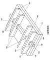
図1は、基板上に形成された、半導体本体上に形成されたいくつかのゲートを含むいくつかのトランジスタの斜視図である。本開示の一実施形態では、基板102は、シャロートレンチ分離(STI)領域などの離間された分離領域104のペアを有する、単結晶シリコンなどのシリコン含有材料であり得、それらの分離領域104のペアはそれらの間に基板活性領域106を画成する。しかしながら、基板102は必ずしもシリコン単結晶基板である必要はなく、ゲルマニウム、ヒ化ガリウム、アンチモン化インジウム、テルル化鉛、ヒ化インジウム、リン化インジウム、アンチモン化ガリウムなど、他のタイプの基板であり得、それらのいずれもシリコンと組み合わされ得る。分離領域104は、基板102においてトレンチを形成し、それらのトレンチを酸化ケイ素(SiO2)などの電気絶縁性材料で埋めることによって形成され得る。
FIG. 1 is a perspective view of several transistors formed on a substrate, including several gates formed on a semiconductor body. In one embodiment of the present disclosure, the
トライゲートトランジスタとして示されている各トランジスタ100は、基板活性領域106に隣接して形成された半導体本体112を含む。半導体本体112は、上面114と、側壁116および対向する側壁118の、横方向に対向する側壁のペアとを有するフィン形構造であり得る。半導体本体112は、単結晶または単一結晶シリコンなど、シリコン含有材料であり得る。本開示の一実施形態では、半導体本体112は基板102と同じ半導体材料から形成され得る。本開示の別の実施形態では、半導体本体112は、基板102を形成するために使用される材料とは異なる半導体材料から形成され得る。本開示のさらに別の実施形態では、半導体本体112は、半導体本体112がその中でひずみを誘起させるように、バルク半導体基板102とは異なる格子定数またはサイズを有する単一の結晶性半導体から形成され得る。
Each
図1にさらに示されているように、半導体本体112にわたって少なくとも1つのゲート122が形成され得る。ゲート122は、半導体本体112の上面114上にまたはそれに隣接して、および横方向に対向する側壁116、118のペア上にまたはそれらに隣接してゲート誘電体層124を形成し、ゲート誘電体層124上にまたはそれに隣接してゲート電極126を形成することによって作製され得る。
As further shown in FIG. 1, at least one
ゲート誘電体層124は、限定はしないが、二酸化ケイ素(SiO2)、酸窒化ケイ素(SiOxNy)、窒化ケイ素(Si3N4)、ならびに酸化ハフニウム、ハフニウムシリコン酸化物、酸化ランタン、ランタンアルミニウム酸化物、酸化ジルコニウム、ジルコニウムシリコン酸化物、酸化タンタル、酸化チタン、バリウムストロンチウムチタニウム酸化物、バリウムチタニウム酸化物、ストロンチウムチタニウム酸化物、酸化イットリウム、酸化アルミニウム、鉛スカンジウムタンタル酸化物、および鉛亜鉛ニオブ酸塩などの高k誘電体材料を含む、任意のよく知られているゲート誘電体材料から形成され得る。ゲート誘電体層124は、当業者には理解されるように、化学気相堆積(「CVD」)、物理気相堆積(「PVD」)、原子層堆積(「ALD」)など、ゲート電極材料を堆積させ、次いで、よく知られているフォトリソグラフィおよびエッチング技法を用いてゲート電極材料をパターニングすることなどによって、よく知られている技法によって形成され得る。
The gate
図1に示されているように、ゲート電極126は、ゲート誘電体層124上にまたはそれに隣接して形成され得る。ゲート電極126は任意の好適なゲート電極材料から形成され得る。本開示の一実施形態では、ゲート電極126は、限定はしないが、ポリシリコン、タングステン、ルテニウム、パラジウム、白金、コバルト、ニッケル、ハフニウム、ジルコニウム、チタン、タンタル、アルミニウム、炭化チタン、炭化ジルコニウム、炭化タンタル、炭化ハフニウム、炭化アルミニウム、他の金属炭化物、金属窒化物、および金属酸化物を含む材料から形成され得る。ゲート電極126は、当業者には理解されるように、ゲート電極材料をブランケット堆積させ、次いで、よく知られているフォトリソグラフィおよびエッチング技法を用いてゲート電極材料をパターニングすることなどによって、よく知られている技法によって形成され得る。
As shown in FIG. 1, the
トランジスタの「幅」は、側壁116における半導体本体112の高さ(図示せず)+上面114における半導体本体112の幅(図示せず)+対向する側壁118における半導体本体112の高さ(図示せず)に等しい。本開示の実装形態では、半導体本体112は、ゲート122に実質的に鉛直な方向に延びている。
The “width” of the transistor is the height of the
ソース領域およびドレイン領域(図示せず)は、半導体本体112においてゲート電極126の両側に形成され得ることを理解されたい。ソースおよびドレイン領域は、N型またはP型導電性など、同じ導電性から形成され得る。ソースおよびドレイン領域は、均一なドーピング濃度を有し得るか、あるいは先端領域(例えば、ソース/ドレイン拡張)など、異なる濃度またはドーピングプロファイルのサブ領域を含み得る。本開示の実施形態のいくつかの実装形態では、ソースおよびドレイン領域は実質的に同じドーピング濃度およびプロファイルを有し得るが、他の実装形態では、それらは異なり得る。
It should be understood that source and drain regions (not shown) may be formed on both sides of the
トランジスタ100の作製では、図2に示されているように、比較的長い半導体本体112および/または本体が形成され得、次いで、ゲート122の形成の前または後のいずれかにおいてギャップ130を形成するためにそれの部分が除去され得る。1つまたは複数のギャップ130の形成は、半導体本体の1つの部分1121を別の部分1122から電気的に絶縁することによって半導体本体の所望の長さを形成する。所望の長さは、半導体本体112の特定の部分に沿って形成されるべきゲート122の数によって決定される。しかしながら、ドライエッチングなど、ギャップ130を形成するためのプロセスは、限定はしないが、当業者には理解されるように、著しい可変性、エッチ偏り、およびフィンの基部における不完全なエッチングを含む問題を有する。当業者には理解されるように、エッチ偏りは、所望の限界寸法よりも大きい幅を有するギャップ130を生じ得、不完全なエッチングは不十分な電気的絶縁を生じ得る。さらに、ひずまされた半導体本体112が有利であるトランジスタデバイスでは、ギャップ130は自由表面エッジを形成し、ギャップ130に近接した半導体本体112上でひずみの緩和を生じ得る。この緩和は、減少関数として、ギャップ130から離れて半導体本体の全長に沿って延長し、それにより、性能が隣のトランジスタとは異なるようになる。
In the fabrication of
図3に示されているように、本開示の一実施形態では、半導体本体112において酸化物分離ゾーン140が形成され得、それにより、酸化物分離ゾーン140によって互いに実質的に電気的に絶縁された、半導体本体の第1の部分1121と、半導体本体の第2の部分1122との形成がもたらされる。酸化物分離ゾーン140は、半導体本体112の一部分を選択的に誘電体酸化物に変換することによって形成され得る。
As shown in FIG. 3, in one embodiment of the present disclosure,
一実施形態では、図4および図5に示されているように、半導体本体112上に酸化触媒層142がパターニングされ得る。図5に示されているように、酸化触媒層142は、当技術分野で知られている任意の技法によって、半導体本体の上面114と、半導体本体の側壁116および118との上に共形に堆積され得る。酸化触媒層142は、下にある半導体本体112の酸化のための触媒として作用することが可能な任意の適切な材料であり得る。一実施形態では、酸化触媒層142は、アルミニウム、酸化アルミニウム、酸化タンタル、酸化イットリウム、酸化ハフニウム、酸化チタン、酸化ジルコニウム、同様の金属またはそれらの関連する酸化物であり得る。特定の実施形態では、半導体本体112はシリコン含有材料であり得、酸化触媒層142は酸化アルミニウムであり得る。一実施形態では、酸化触媒層142は原子層堆積プロセスによって堆積され得、このプロセスは、酸化触媒層142の厚さのばらつきを最小限に抑えるのに役立ち得る。酸化触媒層142は、限定はしないが、フォトリソグラフィおよびエッチング技法を含む、当技術分野で知られている任意の技法によって半導体本体112上にパターニングされ得る。
In one embodiment, an
図6に示されているように、半導体本体112(図5参照)は、酸化触媒層142の下にあるかまたはそれに隣接する半導体本体112(図5参照)を酸化物分離ゾーン140に変換する酸化プロセスにかけられ得る。一実施形態では、酸化プロセスは、例えば乾燥酸化、湿式酸化、高速熱アニールなどの大気酸化の典型的な酸化技法として、またはプラズマ酸化などの準大気技法として実施され得る。酸化触媒層142の存在により、半導体本体112は、酸化触媒層142と接触していない半導体本体112の部分よりも約10倍速い速度で酸化物に変換するようになり得る。これは、酸化触媒層142によって覆われた領域によって画成される酸化をより深くし得る。さらに、深い酸化は酸化触媒層142の接触領域のみにおいて生じるので、酸化物分離ゾーン140の所望の限界寸法が維持され得る。
As shown in FIG. 6, the semiconductor body 112 (see FIG. 5) converts the semiconductor body 112 (see FIG. 5) below or adjacent to the
特定の実施形態では、酸化触媒層142は、シリコンを備える半導体本体112の一部分上に原子層堆積によって堆積された酸化アルミニウムであり得る。半導体本体112および酸化触媒層142は、(必要とされる酸化物の厚さによって決定される)所定の持続時間の間、約400℃から650℃の間の温度(より詳細には、約630℃)において、水素ガスおよび/または酸素ガスの低圧気体混合物に曝露され得る。
In certain embodiments, the
図7に示されているように、酸化物分離ゾーン140の形成の後に、場合によっては酸化触媒層142(図6参照)が除去され得る。酸化物分離ゾーン140は、ゲート122(図3参照)の形成より前にまたはその後に形成され得ることを理解されたい。さらに、明瞭にするために単一の半導体本体112が示されているが、基板102(図1参照)上で互いに実質的に平行に延長している複数の半導体本体112があり得ることを理解されたい。
As shown in FIG. 7, after the formation of the
図8は、本明細書の一実施形態による、非プレーナトランジスタを作製するプロセス200のフローチャートである。ブロック202に記載されているように、半導体本体が形成され得る。ブロック204に記載されているように、半導体本体上に酸化触媒層がパターニングされ得る。ブロック206に記載されているように、酸化触媒層の下にまたはそれに隣接して半導体本体内に酸化物分離ゾーンを形成するために半導体本体が酸化され得る。
FIG. 8 is a flowchart of a
図9は、本明細書の一実装形態によるコンピューティングデバイス300を示す。コンピューティングデバイス300はボード302を収容する。ボード302は、限定はしないが、プロセッサ304および少なくとも1つの通信チップ306A、306Bを含む、いくつかの構成要素を含み得る。プロセッサ304は、ボード302に物理的および電気的に結合される。いくつかの実装形態では、少なくとも1つの通信チップ306A、306Bも、ボード302に物理的および電気的に結合される。さらなる実装形態では、通信チップ306A、306Bはプロセッサ304の一部である。
FIG. 9 illustrates a computing device 300 according to one implementation herein. Computing device 300 houses board 302. The board 302 may include a number of components including, but not limited to, a
コンピューティングデバイス300は、その用途に応じて、ボード302に物理的および電気的に結合されることも結合されないこともある、他の構成要素を含み得る。これらの他の構成要素は、限定はしないが、揮発性メモリ(例えば、DRAM)、不揮発性メモリ(例えば、ROM)、フラッシュメモリ、グラフィックスプロセッサ、デジタル信号プロセッサ、暗号プロセッサ、チップセット、アンテナ、ディスプレイ、タッチスクリーンディスプレイ、タッチスクリーンコントローラ、バッテリー、オーディオコーデック、ビデオコーデック、電力増幅器、全地球測位システム(GPS)デバイス、コンパス、加速度計、ジャイロスコープ、スピーカー、カメラ、および(ハードディスクドライブ、コンパクトディスク(CD)、デジタル多用途ディスク(DVD)などの)大容量ストレージデバイスを含む。 The computing device 300 may include other components that may or may not be physically and electrically coupled to the board 302, depending on the application. These other components include, but are not limited to, volatile memory (eg, DRAM), non-volatile memory (eg, ROM), flash memory, graphics processor, digital signal processor, cryptographic processor, chipset, antenna, Display, touch screen display, touch screen controller, battery, audio codec, video codec, power amplifier, global positioning system (GPS) device, compass, accelerometer, gyroscope, speaker, camera, and (hard disk drive, compact disk ( CD), digital versatile disc (DVD), etc.).
通信チップ306A、306Bは、コンピューティングデバイス300間でデータの転送のためのワイヤレス通信を可能にする。「ワイヤレス」という用語およびそれの派生形は、非固体媒体を通して変調された電磁放射の使用によってデータを通信し得る、回路、デバイス、システム、方法、技法、通信チャネルなどについて説明するために使用され得る。この用語は、関連するデバイスがどんなワイヤも含まないことを暗示するものではないが、いくつかの実施形態では、それらは含まないことがあろう。通信チップ306は、限定はしないが、Wi−Fi(IEEE802.11ファミリー)、WiMAX(IEEE802.16ファミリー)、IEEE802.20、ロングタームエボリューション(LTE)、Ev−DO、HSPA+、HSDPA+、HSUPA+、EDGE、GSM(登録商標)、GPRS、CDMA、TDMA、DECT、Bluetooth(登録商標)、それらの派生物、ならびに3G、4G、5G、およびそれ以降として示される任意の他のワイヤレスプロトコルを含む、いくつかのワイヤレス規格またはプロトコルのいずれかを実装し得る。コンピューティングデバイス300は複数の通信チップ306A、306Bを含み得る。例えば、第1の通信チップ306Aは、Wi−FiおよびBluetooth(登録商標)など、より短距離のワイヤレス通信に専用であり得、第2の通信チップ306Bは、GPS、EDGE、GPRS、CDMA、WiMAX、LTE、Ev−DOなど、より長距離のワイヤレス通信に専用であり得る。
コンピューティングデバイス300のプロセッサ304は、上記で説明した方法で作製された非プレーナトランジスタを含み得る。「プロセッサ」という用語は、レジスタおよび/またはメモリからの電子データを処理して、その電子データをレジスタおよび/またはメモリに記憶され得る他の電子データに変換する任意のデバイスまたはデバイスの部分を指し得る。さらに、通信チップ306A、306Bは、上記で説明した方法で作製された非プレーナトランジスタを含み得る。
The
様々な実装形態では、コンピューティングデバイス300は、ラップトップ、ネットブック、ノートブック、ウルトラブック、スマートフォン、タブレット、携帯情報端末(PDA)、ウルトラモバイルPC、モバイルフォン、デスクトップコンピュータ、サーバ、プリンタ、スキャナ、モニタ、セットトップボックス、エンターテインメントコントロールユニット、デジタルカメラ、ポータブル音楽プレーヤ、またはデジタルビデオレコーダであり得る。さらなる実装形態では、コンピューティングデバイス300は、データを処理する任意の他の電子デバイスであり得る。 In various implementations, the computing device 300 is a laptop, netbook, notebook, ultrabook, smartphone, tablet, personal digital assistant (PDA), ultramobile PC, mobile phone, desktop computer, server, printer, scanner. , Monitors, set-top boxes, entertainment control units, digital cameras, portable music players, or digital video recorders. In further implementations, the computing device 300 may be any other electronic device that processes data.
本明細書の主題は、図1〜図9に示されている特定の適用例に必ずしも限定されるとは限らないことを理解されたい。本主題は、当業者には理解されるように、他のマイクロ電子デバイスおよびアセンブリ適用例、ならびに任意の適切なトランジスタ適用例に適用され得る。 It should be understood that the subject matter herein is not necessarily limited to the particular application shown in FIGS. The present subject matter can be applied to other microelectronic device and assembly applications, as well as any suitable transistor application, as will be appreciated by those skilled in the art.
以下の例はさらなる実施形態に関係し、実施例1は、非プレーナトランジスタを形成する方法であって、半導体本体を形成することと、半導体本体上に酸化触媒層をパターニングすることと、酸化触媒層に隣接して半導体本体内に酸化物分離ゾーンを形成するために半導体本体を酸化させることとを含む方法である。 The following example relates to a further embodiment, and Example 1 is a method of forming a non-planar transistor comprising forming a semiconductor body, patterning an oxidation catalyst layer on the semiconductor body, and an oxidation catalyst. Oxidizing the semiconductor body to form an oxide separation zone in the semiconductor body adjacent to the layer.
実施例2では、実施例1の主題は、半導体本体を酸化させた後に酸化触媒層を除去することを含むことを、場合によっては含むことができる。 In Example 2, the subject matter of Example 1 can optionally include removing the oxidation catalyst layer after oxidizing the semiconductor body.
実施例3では、実施例1から実施例2のいずれかの主題は、半導体本体を形成することが、フィン形構造を形成することを含むことを、場合によっては含むことができる。 In Example 3, the subject matter of any of Examples 1 to 2 can optionally include forming the semiconductor body includes forming a fin-shaped structure.
実施例4では、実施例1から実施例3のいずれかの主題は、半導体本体を形成することが、シリコン含有半導体本体を形成することを含むことを、場合によっては含むことができる。 In Example 4, the subject matter of any of Examples 1 to 3 can optionally include forming a semiconductor body includes forming a silicon-containing semiconductor body.
実施例5では、実施例1から実施例4のいずれかの主題は、半導体本体上に酸化触媒層をパターニングすることが、アルミニウム、酸化アルミニウム、酸化タンタル、酸化イットリウム、酸化ハフニウム、酸化チタン、および酸化ジルコニウムからなる群から選択される材料をパターニングすることを含むことを、場合によっては含むことができる。 In Example 5, the subject matter of any of Examples 1 through 4 includes patterning an oxidation catalyst layer on a semiconductor body, such as aluminum, aluminum oxide, tantalum oxide, yttrium oxide, hafnium oxide, titanium oxide, and It can optionally include patterning a material selected from the group consisting of zirconium oxide.
実施例6では、実施例1から実施例5のいずれかの主題は、半導体本体を形成することが、シリコン半導体本体を形成することを含み、半導体本体上に酸化触媒層をパターニングすることが、シリコン半導体本体上に酸化アルミニウムをパターニングすることを含むことを、場合によっては含むことができる。 In Example 6, the subject matter of any of Examples 1 to 5 includes forming a semiconductor body, forming a silicon semiconductor body, and patterning an oxidation catalyst layer on the semiconductor body. In some cases, including patterning aluminum oxide on the silicon semiconductor body may be included.
実施例7では、実施例1から実施例6のいずれかの主題は、半導体本体を酸化させることが、約400℃から650℃の間の温度において、および大気圧未満の圧力において水素、酸素、亜酸化窒素、および蒸気のうちの少なくとも1つを含む気体混合物に半導体本体を曝露することを含むことを、場合によっては含むことができる。 In Example 7, the subject matter of any of Examples 1 to 6 oxidizes the semiconductor body at a temperature between about 400 ° C. and 650 ° C. and at a pressure below atmospheric pressure, In some cases, including exposing the semiconductor body to a gas mixture comprising at least one of nitrous oxide and vapor.
実施例8では、実施例1から実施例7のいずれかの主題は、半導体本体上に少なくとも1つのトランジスタゲートを形成することを、場合によっては含むことができる。 In Example 8, the subject matter of any of Examples 1-7 can optionally include forming at least one transistor gate on the semiconductor body.
実施例9では、実施例1から実施例8のいずれかの主題は、酸化物分離ゾーンを形成するために、および半導体本体から半導体本体の第1の部分と半導体本体の第2の部分とを形成するために半導体本体を酸化させることを、場合によっては含むことができ、酸化物分離ゾーンは、半導体本体の第1の部分と半導体本体の第2の部分とを実質的に電気的に分離する。 In Example 9, the subject matter of any of Examples 1-8 is to form an oxide isolation zone and from a semiconductor body to a first part of the semiconductor body and a second part of the semiconductor body. Oxidizing the semiconductor body to form may optionally include the oxide isolation zone substantially electrically separating the first portion of the semiconductor body and the second portion of the semiconductor body. To do.
実施例10では、実施例1から実施例9のいずれかの主題は、半導体本体の第1の部分と半導体本体の第2の部分とのうちの少なくとも1つの上に少なくとも1つのトランジスタゲートを形成することを、場合によっては含むことができる。 In Example 10, the subject matter of any of Examples 1-9 includes forming at least one transistor gate on at least one of a first portion of a semiconductor body and a second portion of a semiconductor body. Can be included in some cases.
以下の実施例はさらなる実施形態に関係し、実施例11は、第1の部分と第2の部分とを含む半導体本体と、半導体本体の酸化された部分を備える酸化物分離ゾーンとを備える非プレーナトランジスタであり、酸化物分離ゾーンは、半導体本体の第1の部分と半導体本体の第2の部分とを実質的に電気的に絶縁する。 The following example relates to a further embodiment, and Example 11 comprises a semiconductor body comprising a first part and a second part, and a non-oxide separation zone comprising an oxidized part of the semiconductor body. A planar transistor, the oxide isolation zone substantially electrically isolates the first portion of the semiconductor body from the second portion of the semiconductor body.
実施例12では、実施例11の主題は、半導体本体がシリコン含有材料を備えることを、場合によっては含むことができる。 In Example 12, the subject matter of Example 11 can optionally include that the semiconductor body comprises a silicon-containing material.
実施例13では、実施例11から実施例12のいずれかの主題は、酸化物分離ゾーンが二酸化ケイ素を備えることを、場合によっては含むことができる。 In Example 13, the subject matter of any of Examples 11-12 can optionally include that the oxide separation zone comprises silicon dioxide.
実施例14では、実施例11から実施例13のいずれかの主題は、酸化物分離ゾーンに隣接してパターニングされた酸化触媒層を、場合によっては含むことができる。 In Example 14, the subject matter of any of Examples 11-13 can optionally include an oxidation catalyst layer patterned adjacent to the oxide separation zone.
実施例15では、実施例11から実施例14のいずれかの主題は、酸化触媒層が、アルミニウム、酸化アルミニウム、酸化タンタル、酸化イットリウム、酸化ハフニウム、酸化チタン、および酸化ジルコニウムからなる群から選択される材料を備えることを、場合によっては含むことができる。 In Example 15, the subject matter of any of Examples 11 to 14 is that the oxidation catalyst layer is selected from the group consisting of aluminum, aluminum oxide, tantalum oxide, yttrium oxide, hafnium oxide, titanium oxide, and zirconium oxide. Providing a material that can be optionally included.
実施例16では、実施例11から実施例15のいずれかの主題は、場合によっては、半導体本体の第1の部分と半導体本体の第2の部分とのうちの少なくとも1つの上に少なくとも1つのトランジスタゲートを含むことができる。 In Example 16, the subject matter of any of Examples 11 to 15 optionally includes at least one on at least one of the first portion of the semiconductor body and the second portion of the semiconductor body. A transistor gate can be included.
以下の実施例はさらなる実施形態に関係し、実施例17は、ボードと、ボードに取り付けられたマイクロ電子デバイスとを備える電子システムであり、マイクロ電子デバイスは、第1の部分と第2の部分とを含む半導体本体と、半導体本体の酸化された部分を備える酸化物分離ゾーンとを備える非プレーナトランジスタを含み、酸化物分離ゾーンは、半導体本体の第1の部分と半導体本体の第2の部分とを実質的に電気的に絶縁する。 The following example relates to a further embodiment, and Example 17 is an electronic system comprising a board and a microelectronic device attached to the board, the microelectronic device comprising a first part and a second part. And a non-planar transistor comprising an oxide isolation zone comprising an oxidized portion of the semiconductor body, the oxide isolation zone comprising a first portion of the semiconductor body and a second portion of the semiconductor body. Are substantially electrically isolated from each other.
実施例18では、実施例17の主題は、半導体本体がシリコン含有材料を備えることを、場合によっては含むことができる。 In Example 18, the subject matter of Example 17 can optionally include that the semiconductor body comprises a silicon-containing material.
実施例19では、実施例17から実施例18のいずれかの主題は、酸化物分離ゾーンが二酸化ケイ素を備えることを、場合によっては含むことができる。 In Example 19, the subject matter of any of Examples 17-18 can optionally include that the oxide separation zone comprises silicon dioxide.
実施例20では、実施例17から実施例19のいずれかの主題は、場合によっては、酸化物分離ゾーンに隣接してパターニングされた酸化触媒層を含むことができる。 In Example 20, the subject matter of any of Examples 17-19 can optionally include an oxidation catalyst layer patterned adjacent to the oxide separation zone.
実施例21では、実施例17から実施例20のいずれかの主題は、酸化触媒層が、アルミニウム、酸化アルミニウム、酸化タンタル、酸化イットリウム、酸化ハフニウム、酸化チタン、および酸化ジルコニウムからなる群から選択される材料を備えることを、場合によっては含むことができる。 In Example 21, the subject matter of any of Examples 17 to 20 is that the oxidation catalyst layer is selected from the group consisting of aluminum, aluminum oxide, tantalum oxide, yttrium oxide, hafnium oxide, titanium oxide, and zirconium oxide. Providing a material that can be optionally included.
実施例22では、実施例17から実施例21のいずれかの主題は、場合によっては、半導体本体の第1の部分と半導体本体の第2の部分とのうちの少なくとも1つの上に少なくとも1つのトランジスタゲートを含むことができる。 In Example 22, the subject matter of any of Examples 17-21 includes optionally at least one on at least one of the first portion of the semiconductor body and the second portion of the semiconductor body. A transistor gate can be included.
このように本明細書の実施形態について詳細に説明したが、添付の特許請求の範囲によって定義される本明細書は、それの趣旨または範囲から逸脱することなくそれの多くの明らかな変形形態が可能であるので、上記の説明に記載された特定の詳細によって限定されるものではないことを理解されたい。
[項目1]
非プレーナトランジスタを形成する方法であって、
半導体本体を形成することと、
前記半導体本体上に酸化触媒の層をパターニングすることと、
前記酸化触媒に隣接して前記半導体本体内に酸化物分離ゾーンを形成するために前記半導体本体を酸化させることとを含む方法。
[項目2]
前記半導体本体を酸化させた後に前記酸化触媒の層を除去することをさらに含む、項目1に記載の方法。
[項目3]
前記半導体本体を形成することは、フィン形構造を形成することを含む、項目1に記載の方法。
[項目4]
前記半導体本体を形成することは、シリコン含有半導体本体を形成することを含む、項目1から3のいずれか一項に記載の方法。
[項目5]
前記半導体本体上に酸化触媒の層をパターニングすることは、アルミニウム、酸化アルミニウム、酸化タンタル、酸化イットリウム、酸化ハフニウム、酸化チタン、および酸化ジルコニウムを含む群から選択される材料をパターニングすることを含む、項目1から3のいずれか一項に記載の方法。
[項目6]
前記半導体本体を形成することは、シリコン半導体本体を形成することを含み、前記半導体本体上に前記酸化触媒の層をパターニングすることは、前記シリコン半導体本体上に酸化アルミニウムをパターニングすることを含む、項目1から3のいずれか一項に記載の方法。
[項目7]
前記半導体本体を酸化させることは、約400℃から650℃の間の温度においておよび大気圧未満の圧力において水素、酸素、亜酸化窒素、および蒸気のうちの少なくとも1つの気体混合物に半導体本体を曝露することを含む、項目6に記載の方法。
[項目8]
前記半導体本体上に少なくとも1つのトランジスタゲートを形成することをさらに含む、項目1から3のいずれか一項に記載の方法。
[項目9]
酸化物分離ゾーンを形成するために前記半導体本体を酸化させることは、半導体本体の第1の部分と半導体本体の第2の部分とを形成し、前記酸化物分離ゾーンは、前記半導体本体の第1の部分と前記半導体本体の第2の部分とを実質的に電気的に分離する、項目1から3のいずれか一項に記載の方法。
[項目10]
前記半導体本体の第1の部分と前記半導体本体の第2の部分とのうちの少なくとも1つの上に少なくとも1つのトランジスタゲートを形成することをさらに含む、項目9に記載の方法。
[項目11]
第1の部分と第2の部分とを含む半導体本体と、
前記半導体本体の酸化された部分を備える酸化物分離ゾーンであって、前記半導体本体の第1の部分と前記半導体本体の第2の部分とを実質的に電気的に絶縁する、酸化物分離ゾーンとを備える、非プレーナトランジスタ。
[項目12]
前記半導体本体はシリコン含有材料を備える、項目11に記載の非プレーナトランジスタ。
[項目13]
前記酸化物分離ゾーンは二酸化ケイ素を備える、項目12に記載の非プレーナトランジスタ。
[項目14]
前記酸化物分離ゾーンに隣接してパターニングされた酸化触媒の層をさらに備える、項目11から13のいずれか一項に記載の非プレーナトランジスタ。
[項目15]
前記酸化触媒の層は、アルミニウム、酸化アルミニウム、酸化タンタル、酸化イットリウム、酸化ハフニウム、酸化チタン、および酸化ジルコニウムを含む群から選択される材料を備える、項目14に記載の非プレーナトランジスタ。
[項目16]
前記半導体本体の第1の部分と前記半導体本体の第2の部分とのうちの少なくとも1つの上に少なくとも1つのトランジスタゲートをさらに備える、項目11から13のいずれか一項に記載の非プレーナトランジスタ。
[項目17]
ボードと、
前記ボードに取り付けられたマイクロ電子デバイスであって、前記マイクロ電子デバイスが、第1の部分と第2の部分とを含む半導体本体と、前記半導体本体の酸化された部分を備える酸化物分離ゾーンとを備える少なくとも1つの非プレーナトランジスタを含み、前記酸化物分離ゾーンが、前記半導体本体の第1の部分と前記半導体本体の第2の部分とを実質的に電気的に絶縁する、マイクロ電子デバイスとを備える、電子システム。
[項目18]
前記半導体本体はシリコン含有材料を備える、項目17に記載の電子システム。
[項目19]
前記酸化物分離ゾーンは二酸化ケイ素を備える、項目18に記載の電子システム。
[項目20]
前記酸化物分離ゾーンに隣接してパターニングされた酸化触媒の層をさらに備える、項目17から19のいずれか一項に記載の電子システム。
[項目21]
前記酸化触媒の層は、アルミニウム、酸化アルミニウム、酸化タンタル、酸化イットリウム、酸化ハフニウム、酸化チタン、および酸化ジルコニウムからなる群から選択される材料を備える、項目20に記載の電子システム。
[項目22]
前記半導体本体の第1の部分と前記半導体本体の第2の部分とのうちの少なくとも1つの上に少なくとも1つのトランジスタゲートをさらに備える、項目17から19のいずれか一項に記載の電子システム。
Although embodiments of the present specification have been described in detail, the present specification, as defined by the appended claims, is subject to many obvious variations thereof without departing from the spirit or scope thereof. It should be understood that it is not intended to be limited by the specific details set forth in the foregoing description, where possible.
[Item 1]
A method of forming a non-planar transistor comprising:
Forming a semiconductor body;
Patterning an oxidation catalyst layer on the semiconductor body;
Oxidizing the semiconductor body to form an oxide separation zone in the semiconductor body adjacent to the oxidation catalyst.
[Item 2]
The method of claim 1, further comprising removing the oxidation catalyst layer after oxidizing the semiconductor body.
[Item 3]
The method of claim 1, wherein forming the semiconductor body includes forming a fin-shaped structure.
[Item 4]
4. The method according to any one of items 1 to 3, wherein forming the semiconductor body includes forming a silicon-containing semiconductor body.
[Item 5]
Patterning the layer of oxidation catalyst on the semiconductor body includes patterning a material selected from the group comprising aluminum, aluminum oxide, tantalum oxide, yttrium oxide, hafnium oxide, titanium oxide, and zirconium oxide. 4. The method according to any one of items 1 to 3.
[Item 6]
Forming the semiconductor body includes forming a silicon semiconductor body, and patterning the oxidation catalyst layer on the semiconductor body includes patterning aluminum oxide on the silicon semiconductor body. 4. The method according to any one of items 1 to 3.
[Item 7]
Oxidizing the semiconductor body exposes the semiconductor body to a gas mixture of at least one of hydrogen, oxygen, nitrous oxide, and steam at a temperature between about 400 ° C. and 650 ° C. and at a pressure below atmospheric pressure. The method according to item 6, comprising:
[Item 8]
4. A method according to any one of items 1 to 3, further comprising forming at least one transistor gate on the semiconductor body.
[Item 9]
Oxidizing the semiconductor body to form an oxide isolation zone forms a first portion of the semiconductor body and a second portion of the semiconductor body, and the oxide separation zone includes a second portion of the semiconductor body. 4. A method according to any one of items 1 to 3, wherein a portion of one and a second portion of the semiconductor body are substantially electrically separated.
[Item 10]
10. The method of item 9, further comprising forming at least one transistor gate on at least one of the first portion of the semiconductor body and the second portion of the semiconductor body.
[Item 11]
A semiconductor body including a first portion and a second portion;
An oxide separation zone comprising an oxidized portion of the semiconductor body, wherein the oxide separation zone substantially electrically isolates the first portion of the semiconductor body and the second portion of the semiconductor body. And a non-planar transistor.
[Item 12]
12. A non-planar transistor according to item 11, wherein the semiconductor body comprises a silicon-containing material.
[Item 13]
13. A non-planar transistor according to item 12, wherein the oxide isolation zone comprises silicon dioxide.
[Item 14]
14. A non-planar transistor according to any one of items 11 to 13, further comprising a layer of oxidation catalyst patterned adjacent to the oxide isolation zone.
[Item 15]
15. The non-planar transistor of item 14, wherein the oxidation catalyst layer comprises a material selected from the group comprising aluminum, aluminum oxide, tantalum oxide, yttrium oxide, hafnium oxide, titanium oxide, and zirconium oxide.
[Item 16]
14. A non-planar transistor according to any one of items 11 to 13, further comprising at least one transistor gate on at least one of the first portion of the semiconductor body and the second portion of the semiconductor body. .
[Item 17]
With the board,
A microelectronic device attached to the board, wherein the microelectronic device includes a semiconductor body including a first portion and a second portion, and an oxide isolation zone comprising an oxidized portion of the semiconductor body. A microelectronic device comprising: at least one non-planar transistor comprising: the oxide isolation zone substantially electrically insulating a first portion of the semiconductor body and a second portion of the semiconductor body; An electronic system comprising:
[Item 18]
Item 18. The electronic system of item 17, wherein the semiconductor body comprises a silicon-containing material.
[Item 19]
The electronic system of claim 18, wherein the oxide separation zone comprises silicon dioxide.
[Item 20]
20. The electronic system of any one of items 17-19, further comprising a layer of oxidation catalyst patterned adjacent to the oxide separation zone.
[Item 21]
Item 21. The electronic system of item 20, wherein the oxidation catalyst layer comprises a material selected from the group consisting of aluminum, aluminum oxide, tantalum oxide, yttrium oxide, hafnium oxide, titanium oxide, and zirconium oxide.
[Item 22]
20. The electronic system of any one of items 17 to 19, further comprising at least one transistor gate on at least one of the first portion of the semiconductor body and the second portion of the semiconductor body.
Claims (21)
活性領域を形成する段階と、
前記活性領域の上方に、フィン型の第1トランジスタおよびフィン型の第2トランジスタとを形成する段階と、
前記第1トランジスタのフィン型チャネルと、前記第2トランジスタのフィン型チャネルとを含むフィン型チャネル部を形成する段階と、
前記フィン型チャネル部の第1側面、第2側面、および上面とを覆う酸化触媒層を設ける段階と、
前記酸化触媒層に隣接した前記フィン型チャネル部を酸化して、前記酸化触媒層および前記活性領域に囲まれた酸化物分離ゾーンを形成する段階と、を備え、
前記酸化物分離ゾーンは、前記第1トランジスタおよび前記第2トランジスタを電気的に絶縁する、方法。 A method of manufacturing a non-planar transistor comprising:
Forming an active region; and
Forming a fin-type first transistor and a fin-type second transistor above the active region;
Forming a fin-type channel portion including the fin-type channel of the first transistor and the fin-type channel of the second transistor;
First side of the fin channel portion, providing a second side surface, and oxide catalysts layer covering a top surface,
Wherein the oxidation of the fin channel portion adjacent to the oxidation catalyst layer, and a step of forming an oxide isolation zone surrounded by the oxidation catalyst layer and said active region,
The oxide isolation zone electrically isolates the first transistor and the second transistor.
前記活性領域の上方に設けられたフィン型の第1トランジスタおよびフィン型の第2トランジスタと、
前記第1トランジスタのフィン型チャネルと、前記第2トランジスタのフィン型チャネルとを含むフィン型チャネル部であって、第1側面、第2側面、および上面を有するフィン型チャネル部と、
前記第1側面、前記第2側面、および前記上面を覆う酸化触媒層と、を備え、
前記フィン型チャネル部は、前記酸化触媒層および前記活性領域に囲まれた酸化物分離ゾーンを有し、
前記酸化物分離ゾーンは、前記第1トランジスタと前記第2トランジスタとを電気的に絶縁する、非プレーナトランジスタ。 An active region;
A fin-type first transistor and a fin-type second transistor provided above the active region;
A fin-type channel portion including a fin-type channel of the first transistor and a fin-type channel of the second transistor, the fin-type channel portion having a first side surface, a second side surface, and an upper surface;
An oxidation catalyst layer covering the first side surface, the second side surface, and the upper surface,
The fin-type channel portion has an oxide separation zone surrounded by the oxidation catalyst layer and the active region ,
The oxide isolation zone is a non-planar transistor that electrically insulates the first transistor and the second transistor.
前記ボードに取り付けられたマイクロ電子デバイスとを備え、
前記マイクロ電子デバイスは、
活性領域と、
前記活性領域の上方に設けられたフィン型の第1トランジスタおよびフィン型の第2トランジスタと、
前記第1トランジスタのフィン型チャネルと、前記第2トランジスタのフィン型チャネルとを含むフィン型チャネル部であって、第1側面、第2側面、および上面を含むフィン型チャネル部と、
前記第1側面、前記第2側面、および前記上面とを覆う酸化触媒層と、を含む非プレーナトランジスタを有し、
前記フィン型チャネル部は、前記酸化触媒層および前記活性領域に囲まれた酸化物分離ゾーンを含み、
前記酸化物分離ゾーンは、前記第1トランジスタと前記第2トランジスタとを電気的に絶縁する、電子システム。 With the board,
A microelectronic device attached to the board ;
The microelectronic device is:
An active region;
A fin-type first transistor and a fin-type second transistor provided above the active region;
A fin-type channel portion including a fin-type channel of the first transistor and a fin-type channel of the second transistor, the fin-type channel portion including a first side surface, a second side surface, and an upper surface;
An oxidation catalyst layer that covers the first side surface, the second side surface, and the upper surface; and a non- planar transistor ,
The fin-type channel part includes an oxide separation zone surrounded by the oxidation catalyst layer and the active region ,
The oxide isolation zone insulates said before and Symbol first transistor second transistor electrical manner, electronic system.
Applications Claiming Priority (1)
| Application Number | Priority Date | Filing Date | Title |
|---|---|---|---|
| PCT/US2014/049674 WO2016022098A1 (en) | 2014-08-05 | 2014-08-05 | Apparatus and methods to create microelectronic device isolation by catalytic oxide formation |
Publications (2)
| Publication Number | Publication Date |
|---|---|
| JP2017524257A JP2017524257A (en) | 2017-08-24 |
| JP6376574B2 true JP6376574B2 (en) | 2018-08-22 |
Family
ID=55264233
Family Applications (1)
| Application Number | Title | Priority Date | Filing Date |
|---|---|---|---|
| JP2017505089A Active JP6376574B2 (en) | 2014-08-05 | 2014-08-05 | Non-planar transistors, systems, and methods of manufacturing non-planar transistors including microelectronic device isolation produced by the formation of catalytic oxides |
Country Status (7)
| Country | Link |
|---|---|
| US (1) | US20170162693A1 (en) |
| EP (1) | EP3178115A4 (en) |
| JP (1) | JP6376574B2 (en) |
| KR (1) | KR20170041191A (en) |
| CN (1) | CN106688102B (en) |
| TW (1) | TW201616601A (en) |
| WO (1) | WO2016022098A1 (en) |
Families Citing this family (2)
| Publication number | Priority date | Publication date | Assignee | Title |
|---|---|---|---|---|
| EP3394897A4 (en) * | 2015-12-26 | 2019-08-21 | Intel Corporation | Gate isolation in non-planar transistors |
| US11742410B2 (en) * | 2019-01-03 | 2023-08-29 | Intel Corporation | Gate-all-around integrated circuit structures having oxide sub-fins |
Family Cites Families (16)
| Publication number | Priority date | Publication date | Assignee | Title |
|---|---|---|---|---|
| US4684541A (en) * | 1986-06-11 | 1987-08-04 | Regents Of The University Of Minnesota | Samarium-promoted oxidation of silicon and gallium arsenide surfaces |
| US4806505A (en) * | 1987-10-30 | 1989-02-21 | Regents Of The University Of Minnesota | Samarium- and ytterbium-promoted oxidation of silicon and gallium arsenide surfaces |
| JP2937817B2 (en) * | 1995-08-01 | 1999-08-23 | 松下電子工業株式会社 | Method of forming oxide film on semiconductor substrate surface and method of manufacturing MOS semiconductor device |
| US7098507B2 (en) * | 2004-06-30 | 2006-08-29 | Intel Corporation | Floating-body dynamic random access memory and method of fabrication in tri-gate technology |
| EP1727194A1 (en) * | 2005-05-27 | 2006-11-29 | Interuniversitair Microelektronica Centrum vzw ( IMEC) | Method for high topography patterning |
| US20090020792A1 (en) * | 2007-07-18 | 2009-01-22 | Rafael Rios | Isolated tri-gate transistor fabricated on bulk substrate |
| KR101050457B1 (en) * | 2008-08-29 | 2011-07-19 | 주식회사 하이닉스반도체 | High voltage gate insulating film formation method of semiconductor device |
| US7943511B2 (en) * | 2009-07-17 | 2011-05-17 | United Microelectronics Corp. | Semiconductor process |
| US8269283B2 (en) * | 2009-12-21 | 2012-09-18 | Intel Corporation | Methods and apparatus to reduce layout based strain variations in non-planar transistor structures |
| JP2011216719A (en) * | 2010-03-31 | 2011-10-27 | Toshiba Corp | Method of manufacturing semiconductor device |
| US8278175B2 (en) * | 2010-06-10 | 2012-10-02 | International Business Machines Corporation | Compressively stressed FET device structures |
| US8901537B2 (en) * | 2010-12-21 | 2014-12-02 | Intel Corporation | Transistors with high concentration of boron doped germanium |
| US8492206B2 (en) * | 2011-08-22 | 2013-07-23 | Institute of Microelectronics, Chinese Academy of Sciences | Semiconductor device structure and method for manufacturing the same |
| JP2013084715A (en) * | 2011-10-07 | 2013-05-09 | Toshiba Corp | Nonvolatile semiconductor memory device and method of manufacturing the same |
| US8946792B2 (en) * | 2012-11-26 | 2015-02-03 | International Business Machines Corporation | Dummy fin formation by gas cluster ion beam |
| US8896067B2 (en) * | 2013-01-08 | 2014-11-25 | International Business Machines Corporation | Method of forming finFET of variable channel width |
-
2014
- 2014-08-05 EP EP14899496.5A patent/EP3178115A4/en not_active Withdrawn
- 2014-08-05 JP JP2017505089A patent/JP6376574B2/en active Active
- 2014-08-05 WO PCT/US2014/049674 patent/WO2016022098A1/en active Application Filing
- 2014-08-05 US US15/323,726 patent/US20170162693A1/en not_active Abandoned
- 2014-08-05 CN CN201480080459.5A patent/CN106688102B/en active Active
- 2014-08-05 KR KR1020177001298A patent/KR20170041191A/en not_active Application Discontinuation
-
2015
- 2015-07-01 TW TW104121337A patent/TW201616601A/en unknown
Also Published As
| Publication number | Publication date |
|---|---|
| KR20170041191A (en) | 2017-04-14 |
| JP2017524257A (en) | 2017-08-24 |
| US20170162693A1 (en) | 2017-06-08 |
| WO2016022098A1 (en) | 2016-02-11 |
| CN106688102B (en) | 2021-05-25 |
| EP3178115A1 (en) | 2017-06-14 |
| CN106688102A (en) | 2017-05-17 |
| TW201616601A (en) | 2016-05-01 |
| EP3178115A4 (en) | 2018-03-07 |
Similar Documents
| Publication | Publication Date | Title |
|---|---|---|
| US10790354B2 (en) | Self-aligned gate edge and local interconnect | |
| US11276760B2 (en) | Non-planar semiconductor device having omega-fin with doped sub-fin region and method to fabricate same | |
| US10263112B2 (en) | Vertical non-planar semiconductor device for system-on-chip (SoC) applications | |
| US10998445B2 (en) | Interlayer dielectric for non-planar transistors | |
| CN110047752B (en) | Nanowire transistor fabrication using hardmask layers | |
| EP2647038B1 (en) | Silicon and silicon germanium nanowire structures | |
| US9461143B2 (en) | Gate contact structure over active gate and method to fabricate same | |
| US9780217B2 (en) | Non-planar semiconductor device having self-aligned fin with top blocking layer | |
| CN104160507A (en) | Methods of integrating multiple gate dielectric transistors on a tri-gate (finfet) process | |
| TW201535533A (en) | Techniques for improving gate control over transistor channel by increasing effective gate length | |
| TW201709344A (en) | Dual height glass for FinFET doping | |
| JP6376574B2 (en) | Non-planar transistors, systems, and methods of manufacturing non-planar transistors including microelectronic device isolation produced by the formation of catalytic oxides |
Legal Events
| Date | Code | Title | Description |
|---|---|---|---|
| A621 | Written request for application examination |
Free format text: JAPANESE INTERMEDIATE CODE: A621 Effective date: 20170731 |
|
| A131 | Notification of reasons for refusal |
Free format text: JAPANESE INTERMEDIATE CODE: A131 Effective date: 20180227 |
|
| A977 | Report on retrieval |
Free format text: JAPANESE INTERMEDIATE CODE: A971007 Effective date: 20180228 |
|
| A521 | Request for written amendment filed |
Free format text: JAPANESE INTERMEDIATE CODE: A523 Effective date: 20180528 |
|
| TRDD | Decision of grant or rejection written | ||
| A01 | Written decision to grant a patent or to grant a registration (utility model) |
Free format text: JAPANESE INTERMEDIATE CODE: A01 Effective date: 20180626 |
|
| A61 | First payment of annual fees (during grant procedure) |
Free format text: JAPANESE INTERMEDIATE CODE: A61 Effective date: 20180718 |
|
| R150 | Certificate of patent or registration of utility model |
Ref document number: 6376574 Country of ref document: JP Free format text: JAPANESE INTERMEDIATE CODE: R150 |
|
| R250 | Receipt of annual fees |
Free format text: JAPANESE INTERMEDIATE CODE: R250 |
|
| R250 | Receipt of annual fees |
Free format text: JAPANESE INTERMEDIATE CODE: R250 |
|
| R250 | Receipt of annual fees |
Free format text: JAPANESE INTERMEDIATE CODE: R250 |
|
| R250 | Receipt of annual fees |
Free format text: JAPANESE INTERMEDIATE CODE: R250 |