JP6340216B2 - Scanning electron microscope - Google Patents
Scanning electron microscope Download PDFInfo
- Publication number
- JP6340216B2 JP6340216B2 JP2014045311A JP2014045311A JP6340216B2 JP 6340216 B2 JP6340216 B2 JP 6340216B2 JP 2014045311 A JP2014045311 A JP 2014045311A JP 2014045311 A JP2014045311 A JP 2014045311A JP 6340216 B2 JP6340216 B2 JP 6340216B2
- Authority
- JP
- Japan
- Prior art keywords
- slit
- electron beam
- electron
- selection
- transmittance
- Prior art date
- Legal status (The legal status is an assumption and is not a legal conclusion. Google has not performed a legal analysis and makes no representation as to the accuracy of the status listed.)
- Active
Links
Images


Classifications
-
- H—ELECTRICITY
- H01—ELECTRIC ELEMENTS
- H01J—ELECTRIC DISCHARGE TUBES OR DISCHARGE LAMPS
- H01J37/00—Discharge tubes with provision for introducing objects or material to be exposed to the discharge, e.g. for the purpose of examination or processing thereof
- H01J37/02—Details
- H01J37/04—Arrangements of electrodes and associated parts for generating or controlling the discharge, e.g. electron-optical arrangement, ion-optical arrangement
- H01J37/05—Electron or ion-optical arrangements for separating electrons or ions according to their energy or mass
-
- H—ELECTRICITY
- H01—ELECTRIC ELEMENTS
- H01J—ELECTRIC DISCHARGE TUBES OR DISCHARGE LAMPS
- H01J37/00—Discharge tubes with provision for introducing objects or material to be exposed to the discharge, e.g. for the purpose of examination or processing thereof
- H01J37/02—Details
- H01J37/04—Arrangements of electrodes and associated parts for generating or controlling the discharge, e.g. electron-optical arrangement, ion-optical arrangement
- H01J37/10—Lenses
- H01J37/145—Combinations of electrostatic and magnetic lenses
-
- H—ELECTRICITY
- H01—ELECTRIC ELEMENTS
- H01J—ELECTRIC DISCHARGE TUBES OR DISCHARGE LAMPS
- H01J37/00—Discharge tubes with provision for introducing objects or material to be exposed to the discharge, e.g. for the purpose of examination or processing thereof
- H01J37/02—Details
- H01J37/21—Means for adjusting the focus
-
- H—ELECTRICITY
- H01—ELECTRIC ELEMENTS
- H01J—ELECTRIC DISCHARGE TUBES OR DISCHARGE LAMPS
- H01J37/00—Discharge tubes with provision for introducing objects or material to be exposed to the discharge, e.g. for the purpose of examination or processing thereof
- H01J37/26—Electron or ion microscopes; Electron or ion diffraction tubes
- H01J37/261—Details
- H01J37/263—Contrast, resolution or power of penetration
-
- H—ELECTRICITY
- H01—ELECTRIC ELEMENTS
- H01J—ELECTRIC DISCHARGE TUBES OR DISCHARGE LAMPS
- H01J37/00—Discharge tubes with provision for introducing objects or material to be exposed to the discharge, e.g. for the purpose of examination or processing thereof
- H01J37/26—Electron or ion microscopes; Electron or ion diffraction tubes
- H01J37/28—Electron or ion microscopes; Electron or ion diffraction tubes with scanning beams
-
- H—ELECTRICITY
- H01—ELECTRIC ELEMENTS
- H01J—ELECTRIC DISCHARGE TUBES OR DISCHARGE LAMPS
- H01J37/00—Discharge tubes with provision for introducing objects or material to be exposed to the discharge, e.g. for the purpose of examination or processing thereof
- H01J37/26—Electron or ion microscopes; Electron or ion diffraction tubes
- H01J37/29—Reflection microscopes
- H01J37/292—Reflection microscopes using scanning ray
-
- H—ELECTRICITY
- H01—ELECTRIC ELEMENTS
- H01J—ELECTRIC DISCHARGE TUBES OR DISCHARGE LAMPS
- H01J2237/00—Discharge tubes exposing object to beam, e.g. for analysis treatment, etching, imaging
- H01J2237/05—Arrangements for energy or mass analysis
- H01J2237/057—Energy or mass filtering
-
- H—ELECTRICITY
- H01—ELECTRIC ELEMENTS
- H01J—ELECTRIC DISCHARGE TUBES OR DISCHARGE LAMPS
- H01J2237/00—Discharge tubes exposing object to beam, e.g. for analysis treatment, etching, imaging
- H01J2237/153—Correcting image defects, e.g. stigmators
- H01J2237/1534—Aberrations
-
- H—ELECTRICITY
- H01—ELECTRIC ELEMENTS
- H01J—ELECTRIC DISCHARGE TUBES OR DISCHARGE LAMPS
- H01J2237/00—Discharge tubes exposing object to beam, e.g. for analysis treatment, etching, imaging
- H01J2237/245—Detection characterised by the variable being measured
- H01J2237/24507—Intensity, dose or other characteristics of particle beams or electromagnetic radiation
- H01J2237/24514—Beam diagnostics including control of the parameter or property diagnosed
Description
電子ビームを用いた検査・計測装置に係わる。 The present invention relates to an inspection / measurement apparatus using an electron beam.
電子ビームを用いた試料の観察・検査・計測に用いられる走査電子顕微鏡(SEM)は、電子源から放出された電子を加速し、静電や電磁レンズによって試料表面上に収束させて照射する。これを1次電子と呼んでいる。1次電子の入射によって試料からは2次電子(低エネルギーの電子を2次電子、高エネルギーの電子を反射電子と分けて呼ぶ場合もある。)が放出される。これら2次電子を、電子ビームを偏向して走査しながら検出することで、試料上の微細パターンや組成分布の走査画像を得ることができる。また、試料に吸収される電子を検出することで、吸収電流像を形成することも可能である。 A scanning electron microscope (SEM) used for observation / inspection / measurement of a sample using an electron beam accelerates electrons emitted from an electron source and irradiates them by focusing on the sample surface by electrostatic or electromagnetic lenses. This is called primary electrons. Secondary electrons (low energy electrons are sometimes referred to as secondary electrons and high energy electrons are sometimes referred to as reflected electrons) are emitted from the sample by the incidence of primary electrons. By detecting these secondary electrons while deflecting and scanning the electron beam, it is possible to obtain a scanned image of a fine pattern or composition distribution on the sample. Further, an absorption current image can be formed by detecting electrons absorbed in the sample.
走査電子顕微鏡における基本的な機能の1つは、電子ビームの分解能である。電子ビームの分解能を向上させるために、さまざまな方法が試みられているが、その中の1つにエネルギーフィルタによる電子ビームのエネルギー分散低減技術がある。これはエネルギー分散低減により色収差を低減し、分解能を向上させるものである。エネルギーフィルタは、電子ビームの異なるエネルギーの電子の軌道を分散させる軌道分散器と、分散された電子ビームのエネルギー範囲の選択を行う選択スリットとを持つことでエネルギー分散低減を実現している。電子の軌道を分散させる方法によりオメガフィルタやウイーンフィルタなどと呼ばれる方式に分類される。 One of the basic functions in a scanning electron microscope is the resolution of the electron beam. In order to improve the resolution of the electron beam, various methods have been tried. One of them is a technique for reducing the energy dispersion of the electron beam using an energy filter. This reduces chromatic aberration by reducing energy dispersion and improves resolution. The energy filter achieves energy dispersion reduction by having an orbital disperser that disperses the trajectories of electrons of different energies in the electron beam and a selection slit that selects the energy range of the dispersed electron beam. Depending on the method of dispersing the electron trajectory, it is classified into a system called an omega filter or a Wien filter.
エネルギーフィルタの効果を正しく得るには、電子ビームをスリット上の所望の位置に所望の形状で照射する必要がある。これを達成するために、例えば、特表2002−524818号公報(特許文献1)には、選択スリットを含むプレート上の電子ビームの強度を計測する手法が述べられている。また、特開2011−129257号公報(特許文献2)には、エネルギー選択スリットに流れる電流(スリット電流)を最小にすることでエネルギー選択スリット上の電子ビームの位置を最適化する方法が述べられている。さらに、特開2005−294128号公報(特許文献3)には、スリット選択のための機械的なスリット移動機構が開示されている。 In order to obtain the effect of the energy filter correctly, it is necessary to irradiate the electron beam with a desired shape at a desired position on the slit. In order to achieve this, for example, Japanese Patent Publication No. 2002-524818 (Patent Document 1) describes a technique for measuring the intensity of an electron beam on a plate including a selection slit. Japanese Patent Laid-Open No. 2011-129257 (Patent Document 2) describes a method of optimizing the position of an electron beam on an energy selection slit by minimizing the current (slit current) flowing through the energy selection slit. ing. Furthermore, Japanese Patent Laying-Open No. 2005-294128 (Patent Document 3) discloses a mechanical slit moving mechanism for slit selection.
しかし、これらの特許文献では走査電子顕微鏡を効率良く長期間安定に使用するための観点が不足している。すなわち、効率の良い調整や長時間の安定動作は、装置の実質的な稼働時間を確保するうえで重要であり、特に、半導体製造ラインにて微細パターンの寸法を計測する測長SEM(CDSEM)と呼ばれる走査電子顕微鏡において重視される観点となる。 However, these patent documents lack a viewpoint for using a scanning electron microscope efficiently and stably for a long period of time. In other words, efficient adjustment and long-term stable operation are important in securing the substantial operation time of the apparatus, and in particular, a length measurement SEM (CDSEM) that measures the size of a fine pattern in a semiconductor production line. This is an important point of view in a scanning electron microscope.
具体的には、特許文献1では、選択スリット上で電子ビームを2次元走査する時間が必要となり、電子顕微鏡の本来の目的に使用する時間を削減することになる。また、選択スリット上での2次元走査を頻繁に行うことは電子ビームの不安定性の原因となる可能性があり、出来るだけ避けるべきである。
Specifically, in
また、特許文献2では、装置の長期的安定稼働に対する観点はなく、スリット照射電流の変動に対する考慮もない。
Moreover, in
さらに、特許文献3は、調整用のスリットの機械的移動機構のみが述べられているに過ぎない。
本発明の目的はこれらの課題を解決し、安定なエネルギー分散の低減を実現するエネルギーフィルタを提供することにある。
Furthermore,
An object of the present invention is to solve these problems and to provide an energy filter that realizes stable reduction of energy dispersion.
上記課題を解決するために、例えば特許請求の範囲に記載の構成を採用する。本発明は上記課題を解決する手段を複数含んでいるが、その一例を挙げるならば、電子ビームを発生させる電子源と、電子ビームの異なるエネルギーの電子の軌道を分散させる軌道分散器と、分散された電子ビームのエネルギー範囲の選択を行う選択スリットを有する選択スリット板を有し、選択スリットを透過する電子ビームの透過率をモニターする透過率モニター部を有する。 In order to solve the above problems, for example, the configuration described in the claims is adopted. The present invention includes a plurality of means for solving the above problems. For example, an electron source that generates an electron beam, an orbital disperser that disperses orbits of electrons having different energies in the electron beam, and a dispersion A selection slit plate having a selection slit for selecting the energy range of the electron beam, and a transmittance monitor unit for monitoring the transmittance of the electron beam that passes through the selection slit.
本発明により、選択スリット上の電子ビーム位置に関する情報を効率良くモニターすることが可能で、結果としてエネルギー分散低減や分解能向上の安定化を実現することができる。 According to the present invention, information regarding the position of the electron beam on the selected slit can be monitored efficiently, and as a result, energy dispersion can be reduced and resolution can be stabilized stably.
以下、本発明の実施例について、図面を用いて説明する。 Embodiments of the present invention will be described below with reference to the drawings.
図1に本実施例の走査電子顕微鏡の全体概略図を示す。図1において、電子源100から放出された1次電子116は、第1コンデンサレンズ103、第1静電偏向器150、第1電磁偏向器151、第2静電偏向器160と、第2電磁偏向器161、第2コンデンサレンズ105、対物レンズ113によりステージ115上の試料114に結像される。第1静電偏向器150と第1電磁偏向器151の組は、電子ビームの異なるエネルギーの電子の軌道を分散させる軌道分散器として作用し、選択スリットを挟んで配置された第2静電偏向器160と第2電磁偏向器161は、この軌道の分散の補正光学素子として作用する。第1、第2静電偏向器は偏向色収差の発生効率を向上させるために負の高電圧が印加されている。このために第1、第2静電偏向器は減速型の静電レンズとして作用する効果がある。対物レンズ113上の磁路には正電圧を、試料114には負電圧が印加されており、ここで静電レンズが形成されているため、対物レンズは磁場電場重畳レンズとなっている。またレンズの開口は試料側に向いており、セミインレンズ型と呼ばれるレンズ構造となっている。
FIG. 1 shows an overall schematic diagram of a scanning electron microscope of the present embodiment. In FIG. 1, primary electrons 116 emitted from the electron source 100 are a
試料114から放出される2次電子117(低速電子を2次電子、高速電子を反射電子と分類する場合もあるがここでは2次電子に表記を統一した。)は中間にある検出器121により検出され、2次電子信号を形成する。試料状態が同じであればこの2次電子信号は選択スリットを透過した電流量に対応する。試料上の1次電子は第1走査偏向器106と第2走査偏向器108により2次元に走査され、結果として2次元画像を得ることが出来る。本実施例では第1、第2走査偏向器は静電偏向器である。2次元画像は表示装置147に表示される。ここで第1静電偏向器150と第1電磁偏向器151の組や第2静電偏向器160と第2電磁偏向器161の組を「ExB」(EクロスB)と呼ぶ場合が多い。
The secondary electrons 117 emitted from the sample 114 (the slow electrons are classified as secondary electrons and the fast electrons are sometimes classified as reflected electrons, but here, the notation is unified as secondary electrons) are detected by the
図2は選択スリット板170上の電子ビームの形状を示した図である。第1静電偏向器150と第1電磁偏向器151を、選択スリット302の長手方向に対して直交する方向に逆向き(図2の左右方向)に偏向し、選択スリット板上で偏向色収差のみを発生させている。偏向色収差は横長のビームを作るので、電子ビーム303は横長のビーム形状となっている。この電子ビームの一部を選択スリット302により抽出することでエネルギー分散を低減できる。一般的にこの原理に基づくエネルギーフィルタをウイーンフィルタと呼ぶ。
FIG. 2 is a diagram showing the shape of the electron beam on the selection slit plate 170. The first
また本実施例では、図1に示すように、スリット電流計測部180(例えば電流計)、スリット電流と2次電子信号の比率の計算部181(例えば計算回路とソフトウエア)、その比率の変化量の計算部182(181と計算回路は兼用可能)が設けられている。これらの透過率モニター部により選択スリットを透過する電子ビームの透過率をモニターすることが可能となる。ここで、透過率とは、選択スリット板に当たった電子ビーム量(電流量)に対する選択スリットを透過した電子ビーム量(電流量)の比率としても良いし、選択スリット板に当たった電子ビーム量と選択スリットを透過した電子ビーム量の和と選択スリットを透過した電子ビーム量の比率としても良い。 In this embodiment, as shown in FIG. 1, a slit current measuring unit 180 (for example, an ammeter), a ratio calculating unit 181 (for example, a calculation circuit and software) for the ratio of the slit current and the secondary electron signal, and a change in the ratio An amount calculation unit 182 (181 and the calculation circuit can be used together) is provided. These transmittance monitor units can monitor the transmittance of the electron beam that passes through the selected slit. Here, the transmittance may be the ratio of the amount of electron beam (current amount) transmitted through the selected slit to the amount of electron beam (current amount) hitting the selected slit plate, or the amount of electron beam hitting the selected slit plate. The sum of the amount of electron beams transmitted through the selection slit and the ratio of the amount of electron beams transmitted through the selection slit may be used.
以下に、透過率を測定する必要性とその重要性について述べる。 The necessity and importance of measuring the transmittance are described below.
まず、電子源から放出される電子の電流量は一般的に変動する。電界放出型電子源では特に初期の電流量減少が大きく、ショットキー型電子源でも脈動と呼ばれる電流量の増減がある。従って、選択スリット板に照射される電流量は必ずしも一定ではない。一方、スリット電流や選択スリットを透過した電子から発生する2次電子信号(選択スリットから見ると透過電子信号)の強度は、選択スリット板に照射される電流量と電子ビームのスリット透過率によって決まる。選択スリット板上の電子ビーム位置を一番反映しているのはスリット透過率であるので、スリット電流や選択スリットを透過した電子から発生する2次電子信号の強度単独で電子ビームの位置変動をモニターすることは、モニターの効率を考慮するとメリットがあるが、選択スリット板に照射される電流量に起因した誤差が生じることになる。従って、スリット電流と選択スリットを透過した電子から発生する2次電子信号の強度の比率を求めることにより実質的に透過率に対応するモニター値を得ることが出来る。 First, the amount of current of electrons emitted from the electron source generally varies. In the field emission electron source, the initial decrease in the amount of current is particularly large, and even in the Schottky type electron source, there is an increase or decrease in the amount of current called pulsation. Therefore, the amount of current applied to the selected slit plate is not necessarily constant. On the other hand, the intensity of the secondary electron signal (transmitted electron signal as viewed from the selected slit) generated from the slit current and electrons transmitted through the selected slit is determined by the amount of current applied to the selected slit plate and the slit transmittance of the electron beam. . The most effective reflection of the electron beam position on the selected slit plate is the slit transmittance. Therefore, the position of the electron beam can be changed by the intensity of the secondary electron signal generated from the slit current and the electrons transmitted through the selected slit alone. Although monitoring has an advantage in consideration of the efficiency of the monitor, an error due to the amount of current irradiated to the selected slit plate occurs. Therefore, a monitor value substantially corresponding to the transmittance can be obtained by obtaining the ratio of the intensity of the secondary electron signal generated from the slit current and the electrons transmitted through the selection slit.
また、選択スリット板上での電子ビームの位置変動は透過する電子ビームの特性に影響を与える。直接的な影響は電流量の変化であり、取得画像のSNに影響を与えることになる。この他に重要な特性変化として、中心エネルギーがシフトすることがあげられる。これより試料上での焦点位置が変化し、試料上での電子ビームの分解能が変化する。そして位置変動が更に大きくなると、最終的にはエネルギー分散値が変化することになり、色収差を通して分解能の変動を引き起こす。これら分解能の変動は、特に再現性良く撮像パターン寸法の計測が必要なCDSEMにおいては特性劣化要因として無視できない。従って、正しい電子ビーム位置変動を感知できる透過率をモニター値とすることが装置の安定稼働のために重要となる。 Further, the position variation of the electron beam on the selected slit plate affects the characteristics of the transmitted electron beam. A direct effect is a change in the amount of current, which affects the SN of the acquired image. Another important characteristic change is that the center energy shifts. As a result, the focal position on the sample changes, and the resolution of the electron beam on the sample changes. When the position variation further increases, the energy dispersion value eventually changes, causing a resolution variation through chromatic aberration. Such a variation in resolution cannot be ignored as a factor of characteristic deterioration particularly in a CDSEM that requires measurement of an imaging pattern dimension with good reproducibility. Therefore, it is important for the stable operation of the apparatus to use the transmittance that can sense the correct position change of the electron beam as the monitor value.
本実施例では測定試料ごとに、選択スリット板を流れるスリット電流と、選択スリットの透過電子信号(透過電流量に対応する2次電子117)の強度を測定し、その比率を透過率のモニター値としている。また、その変化を知るために、比率の変化量を計算している。なお、計算する比率の変化量は変化する値の絶対値であってもよいし、相対的変化を示す変化率でもよい。また、計算部181と182は一体化が可能であり、構成要素は共用しても構わない。 In this embodiment, for each measurement sample, the intensity of the slit current flowing through the selected slit plate and the transmitted electron signal (secondary electron 117 corresponding to the amount of transmitted current) of the selected slit is measured, and the ratio is the monitor value of the transmittance. It is said. Further, in order to know the change, the change amount of the ratio is calculated. Note that the change amount of the ratio to be calculated may be an absolute value of a changing value or a change rate indicating a relative change. The calculation units 181 and 182 can be integrated, and the components may be shared.
図3に、本実施例での選択スリット板上の電子ビーム位置の調整処理のフローチャートを示す。図3において、S01で透過率に対応するモニター値を求め透過率を測定する。次に、S02で透過率の初期値からの変化を計算し、S03で、その値が基準値を越えたか否かを判断し、基準値以上の場合は、選択スリット板上での電子ビーム位置が大きくずれたと判定し、S04で選択スリット板上で電子ビームを走査し、S05で選択スリット板上の電子ビーム位置の調整を行う。 FIG. 3 shows a flowchart of the adjustment process of the electron beam position on the selected slit plate in the present embodiment. In FIG. 3, the monitor value corresponding to the transmittance is obtained in S01, and the transmittance is measured. Next, in S02, a change from the initial value of the transmittance is calculated. In S03, it is determined whether or not the value exceeds the reference value. If the value exceeds the reference value, the electron beam position on the selected slit plate is determined. The electron beam is scanned on the selected slit plate in S04, and the position of the electron beam on the selected slit plate is adjusted in S05.
すなわち、透過率を測定することで、電子ビームと選択スリットの相対位置を所定の位置、一般的には電子ビームの中心が選択スリットの中心となる位置、に調整することが出来る。なお、位置調整の具体的処理は、選択スリット板上での電子ビームを偏向走査する偏向走査部として、第1静電偏向器150、第1電磁偏向器151や第1アライナー102等の偏向器、またはスリット移動機構171を用いて電子ビームと選択スリットの相対位置を調整する。
That is, by measuring the transmittance, the relative position between the electron beam and the selection slit can be adjusted to a predetermined position, generally the position where the center of the electron beam is the center of the selection slit. The specific process of position adjustment is performed by using a deflecting scanning unit that deflects and scans an electron beam on the selected slit plate, such as a first
図4に電子ビーム走査による信号例を示す。図4において、(a)は、電子ビーム303と選択スリット302の位置関係を示しており、Y方向には中心が一致しているが、X方向には図の左側に電子ビーム303の中心がずれている場合を示している。この条件で、電子ビームをX,Y方向に走査した場合の選択スリット302を透過した電子から発生する透過電子信号(2次電子信号)のプロファイルを(b)に示す。(b)において、上図がY方向走査位置に対する透過電子信号のプロファイル、下図がX方向走査位置に対する透過電子信号のプロファイルである。選択スリット302の形状と電子ビーム303の形状の長手方向が異なるために、X方向,Y方向で異なった透過電子信号プロファイルを示している。すなわち、(b)上図の、Y方向走査位置に対するプロファイルの場合には、電子ビーム303と選択スリット302のY方向の中心が一致しているので、透過電子信号のプロファイルは走査中心に対して左右対称となる。一方、(b)下図の、X方向走査位置に対するプロファイルの場合には、電子ビーム303の中心が選択スリット302の中心に対して左側にずれているために、例えば電子ビームを選択スリットの右側に全て移動させて透過電子信号をゼロとするためには走査距離が長くなるので、走査中心に対してプロファイル中心が右にずれたプロファイルとなる。すなわち、走査中心とプロファイル中心の差が調整すべき量となる。 FIG. 4 shows an example of signals by electron beam scanning. 4A shows the positional relationship between the electron beam 303 and the selection slit 302. The center of the electron beam 303 coincides with the Y direction, but the center of the electron beam 303 is on the left side of the drawing in the X direction. The case where it has shifted | deviated is shown. Under this condition, a profile of a transmission electron signal (secondary electron signal) generated from electrons transmitted through the selection slit 302 when the electron beam is scanned in the X and Y directions is shown in FIG. In (b), the upper figure shows the profile of the transmitted electron signal with respect to the Y-direction scanning position, and the lower figure shows the profile of the transmitted electron signal with respect to the X-direction scanning position. Since the longitudinal direction of the shape of the selection slit 302 and the shape of the electron beam 303 is different, different transmission electron signal profiles are shown in the X direction and the Y direction. That is, in the case of the profile for the Y-direction scanning position in (b) above, since the center of the electron beam 303 and the selection slit 302 in the Y direction coincides, the profile of the transmitted electron signal is relative to the scanning center. It becomes symmetrical. On the other hand, in the case of the profile for the X-direction scanning position shown in (b) below, the center of the electron beam 303 is shifted to the left with respect to the center of the selection slit 302. Since the scanning distance becomes longer in order to make the transmission electron signal zero by moving all of them, the profile center is shifted to the right with respect to the scanning center. That is, the difference between the scanning center and the profile center is an amount to be adjusted.
本実施例で用いているウイーンフィルタでは2つの偏向器を用いて電子ビームを曲げることなく選択スリットへ照射している。従って、選択スリットへの入射角度が安定であるウイーンフィルタの偏向器を用いることで電子ビーム位置の走査や調整が可能である、といった本実施例を有効に使用できるメリットがある。 In the Wien filter used in this embodiment, two deflectors are used to irradiate the selection slit without bending the electron beam. Therefore, there is an advantage that the present embodiment can be effectively used such that the electron beam position can be scanned and adjusted by using a deflector of a Wien filter whose incident angle to the selected slit is stable.
なお、本実施例ではウエハ毎に透過率をモニターした。これにより電子ビームの試料上での分解能を1.5nm±0.15nmに制御することが可能となった。また、透過率のモニターのタイミングはウエハ毎に限らず、ロット毎や決められた時間毎での運用も可能である。 In this example, the transmittance was monitored for each wafer. As a result, the resolution of the electron beam on the sample can be controlled to 1.5 nm ± 0.15 nm. Further, the monitor timing of the transmittance is not limited to each wafer, and can be operated for each lot or for a predetermined time.
以上説明したように、本実施例は、電子ビームを発生させる電子源と、電子ビームの異なるエネルギーの電子の軌道を分散させる軌道分散器と、分散された電子ビームのエネルギー範囲の選択を行う選択スリットを有する選択スリット板とを有し、前記選択スリットを透過する電子ビームの透過率をモニターする透過率モニター部を有する構成とした。 As described above, in this embodiment, the electron source that generates the electron beam, the orbital disperser that disperses the orbits of the electrons with different energies of the electron beam, and the selection that selects the energy range of the dispersed electron beam. A selection slit plate having a slit, and a transmittance monitor unit for monitoring the transmittance of the electron beam that passes through the selection slit.
また、前記軌道分散器は、重なり合った電磁偏向器と静電偏向器の組からなる構成とすることで、電子ビームの異なるエネルギーの電子の軌道を分散させることが出来る。また、重なり合った第2の電磁偏向器と第2の静電偏向器からなる第2の組を有し、前記組と第2の組が選択スリットを挟んで配置される構成とすることで、軌道の分散の補正光学素子として作用する。 In addition, the orbital disperser is configured by a set of overlapping electromagnetic deflectors and electrostatic deflectors, so that the trajectories of electrons having different energies of the electron beam can be dispersed. Further, by having a second set of overlapping second electromagnetic deflector and second electrostatic deflector, the set and the second set are arranged with a selection slit in between. Acts as a correction optical element for orbital dispersion.
また、前記透過率モニター部は、選択スリットの透過電子信号の計測部と、選択スリット板に流れるスリット電流の計測部と、該2つの計測部からの信号の比率を計算する計算部と、前記比率の変化量を計算する計算部とからなる構成とする。 Further, the transmittance monitor unit includes a transmission electron signal measurement unit for a selection slit, a measurement unit for a slit current flowing through the selection slit plate, a calculation unit for calculating a ratio of signals from the two measurement units, The calculation unit is configured to calculate the amount of change in the ratio.
また、選択スリット上で電子ビームを偏向走査する偏向走査部を有し、透過率の変化が基準値を越えた場合に、偏向走査部により選択スリット上で電子ビームを偏向走査する構成とする。また、前記偏向走査部は、電子ビームを偏向する偏向器または前記選択スリット板を移動させるスリット移動機構である。 In addition, a deflection scanning unit that deflects and scans the electron beam on the selected slit is provided, and when the change in transmittance exceeds a reference value, the electron beam is deflected and scanned on the selected slit by the deflection scanning unit. The deflection scanning unit is a deflector that deflects an electron beam or a slit moving mechanism that moves the selected slit plate.
これにより、選択スリット上の電子ビーム位置に関する情報を効率良くモニターすることが可能で、結果としてエネルギー分散低減や分解能向上の安定化を実現することができる。 As a result, it is possible to efficiently monitor the information related to the position of the electron beam on the selected slit, and as a result, it is possible to realize reduction of energy dispersion and stabilization of resolution.
図5に本実施例の走査電子顕微鏡の全体概略図を示す。実施例1との相違点は、
選択スリット板への電子ビームの照射により生じたスリット2次電子415を検出するスリット検出器411と、そのスリット検出器を制御するスリット検出系制御部412と、選択スリットを透過した透過電子ビーム電流を測定するためのファラデーカップ413と、その電流を計測する透過電流計測部414と、スリット検出器411で検出したスリット2次電子の信号強度を示すスリット信号と透過電流計測部414で計測した透過電流の比率を計算するスリット信号と透過電流の比率の計算部481を有する点である。その他は、実施例1の図1と同様なので説明は省略する。
FIG. 5 shows an overall schematic diagram of the scanning electron microscope of the present embodiment. The difference from Example 1 is
A slit detector 411 for detecting the secondary electrons 415 generated by the irradiation of the electron beam to the selected slit plate, a slit detection system controller 412 for controlling the slit detector, and a transmitted electron beam current transmitted through the selected slit Faraday cup 413 for measuring the current, transmission current measuring unit 414 for measuring the current, slit signal indicating the signal intensity of the secondary electrons detected by the slit detector 411 and transmission measured by the transmission current measuring unit 414 This is a point having a slit signal calculating unit 481 for calculating a current ratio and a ratio of a transmitted current. Others are the same as those of the first embodiment shown in FIG.
すなわち、本実施例では、選択スリット板の選択スリットを透過する透過率を求めるために、スリット電流の代わりに選択スリット板への電子ビームの照射により生じたスリット2次電子415のスリット検出器411で検出した信号強度であるスリット信号(言い換えると、選択スリット板の反射電子信号)と、2次電子117の代わりにファラデーカップ413で測定される選択スリットを透過した透過電子ビーム電流(透過電流)を用いる点で実施例1と相違する。
That is, in the present embodiment, in order to obtain the transmittance that transmits the selected slit of the selected slit plate, the slit detector 411 of the slit secondary electrons 415 generated by the irradiation of the electron beam to the selected slit plate instead of the slit current. The slit signal (in other words, the reflected electron signal of the selected slit plate), which is the signal intensity detected in
従って、本実施例での透過率のモニター値は、スリット2次電子415の信号強度である選択スリット板の反射電子信号と選択スリットの透過電子ビーム電流である透過電流の比率を計算し、その比率の変化量から求めることになる。すなわち、これらの透過率モニター部により選択スリットを透過する電子ビームの透過率をモニターすることが可能となる。 Therefore, the monitor value of the transmittance in this embodiment is obtained by calculating the ratio of the reflected electron signal of the selected slit plate which is the signal intensity of the slit secondary electron 415 and the transmitted current which is the transmitted electron beam current of the selected slit. It is obtained from the amount of change in the ratio. That is, the transmittance of the electron beam that passes through the selected slit can be monitored by these transmittance monitor units.
なお、ファラデーカップでの電流値の測定の際には選択スリットを透過した後の電子ビームの軌道を偏向器により制御することになる。 When measuring the current value in the Faraday cup, the trajectory of the electron beam after passing through the selection slit is controlled by the deflector.
本実施例のメリットは、スリット電流を測定するための絶縁処理や配線が不要になる点と、2次電子が試料の表面状態に影響されるのに対してファラデーカップで測定される選択スリットを透過した透過電子ビーム電流は正確で信頼性が高い点である。 The merit of this embodiment is that the insulation process and wiring for measuring the slit current are not required, and the selection slit that is measured by the Faraday cup while the secondary electrons are affected by the surface state of the sample. The transmitted electron beam current transmitted is accurate and reliable.
なお、実施例1で用いた透過電子信号(2次電子117の信号量)とスリット信号(スリット2次電子415)の組み合わせで透過率をモニターすることも可能である。また、実施例1で用いたスリット電流と透過電流(ファラデーカップで測定される選択スリットを透過した透過電子ビーム電流)の組み合わせで透過率をモニターしても良い。 The transmittance can be monitored by a combination of the transmission electron signal (the signal amount of the secondary electrons 117) and the slit signal (slit secondary electrons 415) used in the first embodiment. Further, the transmittance may be monitored by a combination of the slit current and the transmission current (transmission electron beam current transmitted through the selected slit measured by the Faraday cup) used in the first embodiment.
なお、本実施例ではロット毎に透過率をモニターした。これにより電子ビームの試料上での分解能を1.5nm±0.25nmに制御することが可能となった。 In this example, the transmittance was monitored for each lot. As a result, the resolution of the electron beam on the sample can be controlled to 1.5 nm ± 0.25 nm.
以上説明したように、本実施例は、電子ビームを発生させる電子源と、電子ビームの異なるエネルギーの電子の軌道を分散させる軌道分散器と、分散された電子ビームのエネルギー範囲の選択を行う選択スリットを有する選択スリット板とを有し、前記選択スリットを透過する電子ビームの透過率をモニターする透過率モニター部を有し、該透過率モニター部は、透過電流量の計測部と、選択スリット板の反射電子信号の計測部と、該2つの計測部からの信号の比率を計算する計算部と、前記比率の変化量を計算する計算部とからなる構成とする。 As described above, in this embodiment, the electron source that generates the electron beam, the orbital disperser that disperses the orbits of the electrons with different energies of the electron beam, and the selection that selects the energy range of the dispersed electron beam. A selective slit plate having a slit, and a transmittance monitor unit that monitors the transmittance of an electron beam that passes through the selected slit. The transmittance monitor unit includes a transmission current amount measuring unit, and a selection slit. The reflection electron signal measurement unit of the plate, a calculation unit that calculates the ratio of signals from the two measurement units, and a calculation unit that calculates the amount of change in the ratio are used.
これにより、本実施例では、選択スリット上の電子ビーム位置に関する情報を効率良くモニターすることが可能で、結果としてエネルギー分散低減や分解能向上の安定化を実現することができる。 As a result, in this embodiment, it is possible to efficiently monitor the information regarding the electron beam position on the selected slit, and as a result, it is possible to realize stabilization of energy dispersion reduction and resolution improvement.
本実施例は、選択スリット板の選択スリットを透過する透過率を直接求める例を示す。図6は、本実施例で用いる選択スリット板と電子ビームを示した図である。他の全体構成は、実施例1または2と同様である。 The present embodiment shows an example in which the transmittance that passes through the selection slit of the selection slit plate is directly obtained. FIG. 6 is a diagram showing a selective slit plate and an electron beam used in this embodiment. Other overall configurations are the same as those in the first or second embodiment.
図6において、選択スリット板500は、エネルギー分散低減のための選択スリット501の近傍に、実質的に電子ビーム全体を透過させることの出来る大きなサイズの開口(透過開口503)を有している。本実施例では電子ビームを2つの開口(選択スリット501と透過開口503)間で電気的に移動させ、2つの透過電子信号または透過電流を測定する。そしてこの2つの値の比率から、電子源から発生する電子ビーム全体に対する選択スリットを透過する電子ビームの割合として電子ビームの透過率を求め、モニター値としている。すなわち、これらの透過率モニター部により選択スリットを透過する電子ビームの透過率をモニターすることが可能となる。本実施例のメリットは、透過率の測定にスリット電流やスリット2次電子の測定が不要であり、透過率が絶対値として求まることにある。 In FIG. 6, the selective slit plate 500 has a large-sized opening (transmission opening 503) capable of transmitting substantially the entire electron beam in the vicinity of the selection slit 501 for reducing energy dispersion. In this embodiment, an electron beam is electrically moved between two openings (selection slit 501 and transmission opening 503), and two transmission electron signals or transmission currents are measured. Then, from the ratio of these two values, the transmittance of the electron beam is obtained as the ratio of the electron beam that passes through the selected slit to the entire electron beam generated from the electron source, and is used as the monitor value. That is, the transmittance of the electron beam that passes through the selected slit can be monitored by these transmittance monitor units. The merit of the present embodiment is that the measurement of the transmittance does not require the measurement of the slit current or the slit secondary electrons, and the transmittance can be obtained as an absolute value.
以上説明したように、本実施例は、選択スリット板として、選択スリットの近傍に電子ビームの全体を透過させる透過開口を有し、透過率モニター部は、選択スリットを透過する透過電子信号もしくは透過電流の第1の計測値と、前記透過開口を透過する透過電子信号もしくは透過電流の第2の計測値を計測する計測部と、前記第1と第2の計測値の比率を計算する計算部と、前記比率の変化量を計算する計算部とからなる構成とする。 As described above, this embodiment has a transmission aperture that transmits the entire electron beam in the vicinity of the selection slit as the selection slit plate, and the transmittance monitor unit transmits a transmission electron signal or transmission that transmits the selection slit. A first measurement value of current, a measurement unit that measures a second measurement value of a transmission electron signal or transmission current that is transmitted through the transmission aperture, and a calculation unit that calculates a ratio of the first and second measurement values And a calculation unit for calculating the amount of change in the ratio.
これにより、本実施例では、選択スリット上の電子ビーム位置に関する情報を効率良くモニターすることが可能で、結果としてエネルギー分散低減や分解能向上の安定化を実現することができるという効果に加えて、透過率の測定にスリット電流やスリット2次電子の測定が不要であり、透過率が絶対値として求まるという効果がある。 Thereby, in the present embodiment, it is possible to efficiently monitor the information regarding the electron beam position on the selected slit, and as a result, it is possible to realize stabilization of energy dispersion reduction and resolution improvement, The measurement of the transmittance does not require the measurement of the slit current or the slit secondary electrons, and the transmittance can be obtained as an absolute value.
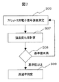
本実施例は、前記したスリット2次電子の信号強度を利用して、電子ビームの透過率をモニターするタイミングを決める基準とする例について説明する。 In the present embodiment, an example will be described in which the signal intensity of the slit secondary electrons is used as a reference for determining the timing for monitoring the transmittance of the electron beam.
すなわち、スリット2次電子信号は常時計測が可能であり、本来の目的に使用する時間を削減することはない。また、この信号の変化をモニターすることで何らかの異常検知は期待できる。しかし、前に述べたように照射電子ビームの変動があるために選択スリット板上の電子ビームの位置のモニターとしては不完全である。従って、本実施例ではスリット2次電子の信号強度変化が基準値を越えた場合に透過率を測定し、電子ビーム位置を調整する必要があるか判定することとした。 That is, the slit secondary electron signal can always be measured, and the time used for the original purpose is not reduced. In addition, monitoring of this signal change can be expected to detect any abnormality. However, since the irradiation electron beam varies as described above, it is imperfect as a monitor of the position of the electron beam on the selective slit plate. Therefore, in this embodiment, when the signal intensity change of the secondary electrons of the slit exceeds the reference value, the transmittance is measured to determine whether the electron beam position needs to be adjusted.
図7に、スリット2次電子の信号強度を利用した透過率測定タイミングのフローチャートを示す。図7において、S06でスリット2次電子の信号強度を測定する。具体的な構成は、図5のスリット検出器411により検出する。そして、S07で信号強度の変化率を計算する。そして、S08で、その値が基準値を越えたか否かを判断し、基準値以上の場合は、S09で透過率の測定を実施する。
なお、ここでは信号強度の変化する変化量として相対的変化を示す変化率で説明したが、変化する値の絶対値であってもよい。
FIG. 7 shows a flowchart of the transmittance measurement timing using the signal intensity of the slit secondary electrons. In FIG. 7, the signal intensity of the slit secondary electrons is measured in S06. A specific configuration is detected by the slit detector 411 in FIG. In step S07, the signal intensity change rate is calculated. Then, in S08, it is determined whether or not the value exceeds the reference value. If the value exceeds the reference value, the transmittance is measured in S09.
Here, the change rate indicating the relative change is described as the change amount of the signal intensity, but may be an absolute value of the changing value.
以上、本実施例では、電子ビームの透過率をモニターするタイミングを決める基準としてスリット2次電子信号の強度を利用する点を説明したが、この考え方は他の信号(スリット電流、透過電子信号、透過電流)にも適用可能である。また、このタイミングと並行してウエハ毎やロット毎の透過率のモニターを行うことは有効と考えられる。 As described above, in the present embodiment, the point that the intensity of the secondary electron signal of the slit is used as a reference for determining the timing for monitoring the transmittance of the electron beam, but this idea is based on other signals (slit current, transmitted electron signal, (Transmission current). In addition, it is considered effective to monitor the transmittance for each wafer or lot in parallel with this timing.
なお、本実施例とロット毎の透過率のモニターを組み合わせることで電子ビームの試料上での分解能を1.5nm±0.15nmに制御することが可能となった。 In addition, it became possible to control the resolution of the electron beam on the sample to 1.5 nm ± 0.15 nm by combining this embodiment with a monitor for transmittance for each lot.
以上説明したように、本実施例は、選択スリットの透過電子信号もしくは透過電流もしくは選択スリット板の反射電子信号あるいは選択スリット板に流れるスリット電流を測定し、該測定値の変化量が基準値を越えた場合に、透過率モニター部で選択スリットでの電子ビームの透過率を計測する構成とする。これにより、電子ビームの透過率をモニターするタイミングを決めることが出来る。 As described above, this embodiment measures the transmission electron signal or transmission current of the selection slit, the reflection electron signal of the selection slit plate, or the slit current flowing through the selection slit plate, and the amount of change in the measured value is the reference value. When it exceeds, the transmittance monitor unit measures the transmittance of the electron beam at the selected slit. Thereby, the timing for monitoring the transmittance of the electron beam can be determined.
本実施例は、選択スリット板上の電子ビーム位置調整の実施可否判断と、位置調整の具体的処理判断の例について説明する。 In the present embodiment, an example of determining whether or not to perform the electron beam position adjustment on the selected slit plate and a specific process determination of the position adjustment will be described.
本実施例の処理フローを図8に示す。本実施例に係る全体構成は、図1または図5と同じであり、処理フローとして、基準値を複数設けている点で、図3と異なる。 A processing flow of this embodiment is shown in FIG. The overall configuration according to the present embodiment is the same as that of FIG. 1 or FIG. 5, and is different from FIG. 3 in that a plurality of reference values are provided as a processing flow.
図8において、S10、S11、S12で透過率をモニターし変化が第1基準値未満か判定する。これは、図3のS01、S02、S03と同様の処理である。第1基準値以上の場合は、選択スリット板上での電子ビーム位置が大きくずれたと判定し、電子ビーム位置調整の実施に移る。 In FIG. 8, the transmittance is monitored in S10, S11, and S12 to determine whether the change is less than the first reference value. This is the same processing as S01, S02, and S03 in FIG. If it is greater than or equal to the first reference value, it is determined that the position of the electron beam on the selected slit plate has greatly deviated, and the process moves to the adjustment of the electron beam position.
ここで、位置調整は、実施例1でも説明したように、選択スリット板上での電子ビームの偏向走査により偏向走査部により実施する。その具体的手段として、第1静電偏向器150、第1電磁偏向器151や第1アライナー102のような偏向器による補正によりスリット上のビーム位置を調整する方法と、スリット移動機構171による機械的なスリットステージの駆動により相対的な電子ビーム位置の調整を行なう方法がある。偏向器による調整では偏向器補正の累積値が大きくなると電子ビームの軌道のずれが大きくなる。また、スリットステージの駆動による機械的な位置制御は電気的な電子ビームの位置制御ほど位置分解能がないが、大きく動かすことが可能であり、両者をうまく使い分けることが重要である。
Here, as described in the first embodiment, the position adjustment is performed by the deflection scanning unit by the deflection scanning of the electron beam on the selected slit plate. As specific means, a method of adjusting the beam position on the slit by correction by a deflector such as the first
よって、S13において偏向器補正の累積値を参照し、S14で、その値が第2基準値以上であるかを判定し、第2基準値以下の場合は、S15で偏向器による偏向量の強度調整を行うことでスリット上のビーム位置を調整する。一方、第2基準値以上の場合は、S16で、電子ビームの軌道のずれが大きくなるために、スリットステージの駆動により移動調整を行い相対的な電子ビーム位置の調整を行う。 Accordingly, the accumulated value of the deflector correction is referred to in S13, and it is determined in S14 whether the value is equal to or greater than the second reference value. If the value is equal to or less than the second reference value, the intensity of the deflection amount by the deflector is determined in S15. The beam position on the slit is adjusted by performing the adjustment. On the other hand, if the value is equal to or greater than the second reference value, the displacement of the electron beam trajectory becomes large in S16, so that the movement is adjusted by driving the slit stage and the relative electron beam position is adjusted.
なお、スリットステージの駆動を行う場合は電子ビームの光学的な軸調整も併用し、偏向器制御は初期状態に戻すことが望ましい。 When the slit stage is driven, it is desirable that the optical axis adjustment of the electron beam is also used and the deflector control is returned to the initial state.
以上説明したように、本実施例は、選択スリット板上での電子ビームの偏向走査にあたって、偏向器による電子ビーム補正の累積値が第2の基準値より大きいかを判断し、該累積値が第2の基準値未満であれば前記偏向器による電子ビーム位置調整を行い、該累積値が第2の基準値以上であればスリット移動機構による選択スリット位置調整を行う構成とした。これにより、選択スリット板上の電子ビーム位置調整において、位置分解能による精度と位置調整スピードの両方を考慮した調整が可能となる。 As described above, this embodiment determines whether the accumulated value of the electron beam correction by the deflector is larger than the second reference value in the deflection scanning of the electron beam on the selected slit plate, and the accumulated value is If it is less than the second reference value, the position of the electron beam is adjusted by the deflector, and if the accumulated value is greater than or equal to the second reference value, the selected slit position is adjusted by the slit moving mechanism. As a result, in the electron beam position adjustment on the selected slit plate, it is possible to perform adjustment in consideration of both accuracy due to position resolution and position adjustment speed.
本実施例では、焦点補正について説明する。 In this embodiment, focus correction will be described.
前述したように、選択スリット板上の電子ビームの移動は電子ビームのエネルギーの中心値をシフトさせる。このことは電子ビームの試料面上での焦点位置を変化させるため、分解能の変動の原因となる。汎用SEMではマニュアルによる焦点補正を常時行うために実質的にこの変動は顕在化しにくい。しかし、測長SEMの様に撮像以外の動作を避けたい装置の場合は焦点補正の回数を出来るだけ抑えることが好ましい。従って、本実施例では、透過率をモニターし、その変化が基準値以上の場合に焦点補正を行うようにした。なお、本実施例の走査電子顕微鏡の全体構成は、実施例1または2と同様である。 As described above, the movement of the electron beam on the selected slit plate shifts the center value of the energy of the electron beam. This changes the focal position of the electron beam on the sample surface, which causes variations in resolution. In general-purpose SEMs, manual focus correction is always performed, so this variation is hardly realized. However, in the case of an apparatus that wants to avoid operations other than imaging, such as a length measurement SEM, it is preferable to suppress the number of focus corrections as much as possible. Therefore, in this embodiment, the transmittance is monitored, and the focus correction is performed when the change is equal to or greater than the reference value. The overall configuration of the scanning electron microscope of this example is the same as that of Example 1 or 2.
図9に本実施例のフローチャートを示す。図9において、S17、S18、S19で透過率をモニターし変化が基準値未満か判定する。なお、S18ではモニター値の変化する変化量として相対的変化を示す変化率で説明したが、変化する値の絶対値であってもよい。また、透過率のモニター値としては、実施例1または2と同様の、選択スリットの透過電子信号もしくは透過電流もしくは選択スリット板の反射電子信号あるいは選択スリット板に流れるスリット電流である。 FIG. 9 shows a flowchart of this embodiment. In FIG. 9, the transmittance is monitored in S17, S18, and S19 to determine whether the change is less than the reference value. In S18, the change rate indicating the relative change is described as the change amount of the monitor value. However, the absolute value of the change value may be used. The monitor value of the transmittance is the transmission electron signal or transmission current of the selection slit, the reflection electron signal of the selection slit plate, or the slit current flowing through the selection slit plate, as in the first or second embodiment.
そして、モニター値が基準値を越えた場合に、S20で焦点補正を行う。このようにすれば、分解能の変動を少ない回数の焦点補正動作で抑制することが可能である。 When the monitor value exceeds the reference value, focus correction is performed in S20. In this way, it is possible to suppress fluctuations in resolution with a small number of focus correction operations.
なお、焦点補正用の基準値は、実施例5の電子ビーム位置調整の実施可否判断のための第1の基準値より小さい。また、焦点補正は通常よく行われる対物電磁コイルの電流を変化させても良いが、ここではステージ電圧を変化させることで対応する。焦点変化の原因が電子ビームのエネルギーの変化であるために試料への照射エネルギーを一定に保つために、ステージ電圧を変化させることとした。 The reference value for focus correction is smaller than the first reference value for determining whether or not to perform the electron beam position adjustment of the fifth embodiment. In addition, focus correction may be performed by changing the current of the objective electromagnetic coil that is usually performed, but here, it is handled by changing the stage voltage. Since the cause of the focus change is a change in the energy of the electron beam, the stage voltage was changed in order to keep the irradiation energy to the sample constant.
なお、本実施例と30分毎の透過率のモニターを組み合わせることで電子ビームの試料上での分解能を1.5nm±0.1nmに制御することが可能となった。 In addition, it became possible to control the resolution of the electron beam on the sample to 1.5 nm ± 0.1 nm by combining this embodiment with a monitor for transmittance every 30 minutes.
以上説明したように、本実施例は、電子ビームを発生させる電子源と、電子ビームの異なるエネルギーの電子の軌道を分散させる軌道分散器と、分散された電子ビームのエネルギー範囲の選択を行う選択スリットを有する選択スリット板と、試料に電子ビームを照射する対物レンズと、試料を置くステージと、選択スリットの透過電子信号もしくは透過電流もしくは選択スリット板の反射電子信号あるいは選択スリット板に流れるスリット電流をモニターする透過率モニター部を有し、該モニター値の変化量が基準値より大きくなった場合に前記試料上での焦点補正を行う構成とした。これにより、分解能の変動を少ない回数の焦点補正動作で抑制することが可能となる。 As described above, in this embodiment, the electron source that generates the electron beam, the orbital disperser that disperses the orbits of the electrons with different energies of the electron beam, and the selection that selects the energy range of the dispersed electron beam. A selection slit plate having a slit, an objective lens for irradiating the sample with an electron beam, a stage on which the sample is placed, a transmission electron signal or transmission current of the selection slit, a reflection electron signal of the selection slit plate, or a slit current flowing through the selection slit plate And a transmittance monitor section for monitoring the above-mentioned, and when the amount of change in the monitored value is larger than the reference value, the focus correction on the sample is performed. As a result, it is possible to suppress fluctuations in resolution with a small number of focus correction operations.
本実施例は、電子ビーム形状について説明する。 In this embodiment, an electron beam shape will be described.
図10は、本実施例における選択スリット板上の電子ビームの形状を示す図である。図10において、電子ビームの形状は、図2と比較して、選択スリット3002の長手方向に幅を持っている。 FIG. 10 is a diagram showing the shape of the electron beam on the selected slit plate in the present embodiment. In FIG. 10, the shape of the electron beam has a width in the longitudinal direction of the selection slit 3002 as compared with FIG.
通常、選択スリットに照射する電子ビームは、図11に示すようにスリット上で合焦点を形成する。これはエネルギー分散の選択スリットによる選択性を高めるためである。しかし、選択スリットの長手方向に対しては必ずしもその必要はない。また、図11に示したように、本実施例ではスリット電流値と透過電流値の比率から電子ビームの透過率をモニターしている。ミクロンオーダー以下の微小なサイズのスリットを作る場合は、選択スリットの長手方向の長さにも限界があり、従って、選択スリットの長手方向の電子ビーム位置変化にも注意を払う必要がある。その際、図2のような選択スリットの長手方向に幅のない電子ビーム形状では、電子ビームが選択スリットの長手方向の端に到達した場合に急に透過電流が減少することになり、透過率のモニターが異常を発見するのが遅れることになる。 Usually, the electron beam irradiated to the selection slit forms a focal point on the slit as shown in FIG. This is for enhancing the selectivity by the selective slit for energy dispersion. However, this is not always necessary in the longitudinal direction of the selection slit. As shown in FIG. 11, in this embodiment, the transmittance of the electron beam is monitored from the ratio between the slit current value and the transmitted current value. When making a slit having a minute size of the order of micron or less, there is a limit to the length in the longitudinal direction of the selection slit. Therefore, attention must be paid to the change in the electron beam position in the longitudinal direction of the selection slit. At that time, in the electron beam shape having no width in the longitudinal direction of the selection slit as shown in FIG. 2, when the electron beam reaches the end in the longitudinal direction of the selection slit, the transmission current suddenly decreases, and the transmittance Your monitor will be late to discover the anomaly.
したがって、選択スリットの長手方向の電子ビームの位置変動に対する感度を低下させるために、電子ビームの選択スリットの長手方向、言い換えれば、電子ビームの軌道を分散させる方向とおおよそ垂直方向、を合焦点の場合より幅を大きくして選択スリット板に照射することが望ましい。 Therefore, in order to reduce the sensitivity to the fluctuation of the position of the electron beam in the longitudinal direction of the selected slit, the longitudinal direction of the selected slit of the electron beam, in other words, the direction in which the trajectory of the electron beam is dispersed and the direction substantially perpendicular to it are focused. It is desirable to irradiate the selective slit plate with a larger width than the case.
具体的実現手段としては、選択スリット板上での焦点状態をデフォーカス状態にするか、非点収差とデフォーカスを組み合わせて、電子ビームの選択スリットの長手方向のみ幅を持たせる手法が有効である。 As a concrete realization means, it is effective to set the focus state on the selected slit plate to a defocused state or combine astigmatism and defocus so that only the longitudinal direction of the selected slit of the electron beam has a width. is there.
本実施例は、モニター画面例について説明する。 In this embodiment, an example of a monitor screen will be described.
図12は、本実施例におけるモニター画面を示す図である。図12において、画面にはモニター値、モニター頻度、基準値レベルの選択結果が表示されている。また、過去のモニター値の変化を示すグラフが描かれている。また、モニター履歴のON、OFF表示も設けている。これらを参考にして装置状態に適したモニター方法を選択することができる。 FIG. 12 is a diagram showing a monitor screen in the present embodiment. In FIG. 12, the selection result of the monitor value, the monitor frequency, and the reference value level is displayed on the screen. In addition, a graph showing changes in past monitor values is drawn. In addition, monitor history ON / OFF display is also provided. A monitoring method suitable for the state of the apparatus can be selected with reference to these.
本実施例は、基準値の設定について説明する。 In this embodiment, setting of a reference value will be described.
前述した各実施例で用いた基準値は、装置の必要とする分解能やスループット等によって変わるので、適宜設定する必要がある。その値は、事前に設定しても良いし、実測しながらその都度設定してもよい。事前に設定する場合には、例えばテーブルとして、図1の記録装置145にあらかじめ記録しておき、設定時にそのテーブルを参照して設定する。
Since the reference value used in each of the above-described embodiments varies depending on the resolution and throughput required by the apparatus, it is necessary to set appropriately. The value may be set in advance or may be set each time while actually measuring. In the case of setting in advance, for example, a table is recorded in advance in the
図13に、選択スリット板上の電子ビーム位置の調整を行うための透過率の変化率の基準値の場合について、モード別の設定値テーブルを示す。図13において、例えば、高分解能モード1であれば、その基準値は小として、きめ細かく制御を行う。また、高速モード2では、スループットを優先として、細かな調整は省くモードであり、その時の基準値は大とする。また、大電流モード3では、信号強度を保持するために大電流を流すモードであり、その時の基準値は中とする。さらに、高焦点深度モード4の場合も、その時の基準値は中とする。
FIG. 13 shows a setting value table for each mode in the case of the reference value of the change rate of transmittance for adjusting the electron beam position on the selected slit plate. In FIG. 13, for example, in the
以上実施例について説明したが、本発明は上記した実施例に限定されるものではなく、様々な変形例が含まれる。例えば、本実施例ではウイーンフィルタの実施例についてのみ記載したが、オメガフィルタやガンマフィルタといった他の方式のエネルギーフィルタにも有効である。また、ある実施例の構成の一部を他の実施例の構成に置き換えることが可能であり、また、ある実施例の構成に他の実施例の構成を加えることも可能である。また、各実施例の構成の一部について、他の構成の追加、削除、置換をすることも可能である。 Although the embodiments have been described above, the present invention is not limited to the above-described embodiments, and includes various modifications. For example, in the present embodiment, only the Wien filter embodiment has been described, but the present invention is also effective for other types of energy filters such as an omega filter and a gamma filter. Further, a part of the configuration of one embodiment can be replaced with the configuration of another embodiment, and the configuration of another embodiment can be added to the configuration of one embodiment. Moreover, it is also possible to add, delete, and replace other configurations for a part of the configuration of each embodiment.
100:電子源、101:電子銃、102:第1アライナー、
103:第1コンデンサレンズ、105:第2コンデンサレンズ、
106:第1走査偏向器、108:第2走査偏向器、113:対物レンズ、
114:試料、115:ステージ、116:1次電子、117:2次電子、
121:検出器、131:電子銃制御部、132:第1アライナー制御部、
133:第1コンデンサレンズ制御部、135:第2コンデンサレンズ制御部、136:検出系制御部、137:第1走査偏向器制御部、
139:第2走査偏向器制御部、141:ブースター電圧制御部、
142:対物レンズ制御部、144:試料電圧制御部、145:記録装置、
146:装置全体の制御演算装置、147:表示装置、
150:第1静電偏向器、151:第1電磁偏向器、160:第2静電偏向器、
161:第2電磁偏向器、170:選択スリット板、171:スリット移動機構、
172:スリット制御部、180:スリット電流計測部、
181:スリット電流と2次電子信号の比率の計算部、
182:比率の変化の計算部、302:選択スリット、303:電子ビーム、
304:スリット上での偏向色収差発生方向、411:スリット検出器、
412:スリット検出系制御部、413:ファラデーカップ、
414:透過電流計測部、415:スリット2次電子、500:選択スリット板、
501:選択スリット、502:電子ビーム、503:透過開口、
481:スリット信号と透過電流の比率の計算部、701:選択スリット、
702:電子ビーム、1001:選択スリット板、1002:選択スリット、
1003:電子ビーム、1004:スリット上での偏向色収差発生方向、
1101:電子ビーム、1102:ExB、1103:選択スリット、
1104:スリット電流計、1105:透過電流計、1106:演算装置
100: electron source, 101: electron gun, 102: first aligner,
103: first condenser lens, 105: second condenser lens,
106: first scanning deflector, 108: second scanning deflector, 113: objective lens,
114: Sample, 115: Stage, 116: Primary electron, 117: Secondary electron,
121: detector, 131: electron gun controller, 132: first aligner controller,
133: first condenser lens controller, 135: second condenser lens controller, 136: detection system controller, 137: first scanning deflector controller,
139: Second scanning deflector controller 141: Booster voltage controller
142: objective lens control unit, 144: sample voltage control unit, 145: recording device,
146: Control arithmetic device for the entire device, 147: Display device,
150: first electrostatic deflector, 151: first electromagnetic deflector, 160: second electrostatic deflector,
161: second electromagnetic deflector, 170: selection slit plate, 171: slit moving mechanism,
172: Slit control unit, 180: Slit current measurement unit,
181: a calculation unit for the ratio of the slit current and the secondary electron signal,
182: ratio change calculation unit, 302: selection slit, 303: electron beam,
304: Direction of occurrence of deflection chromatic aberration on the slit, 411: Slit detector,
412: Slit detection system control unit, 413: Faraday cup,
414: Transmitted current measurement unit, 415: Slit secondary electron, 500: Selection slit plate,
501: selective slit, 502: electron beam, 503: transmission aperture,
481: Calculation part of ratio of slit signal and transmitted current, 701: Selected slit,
702: Electron beam, 1001: Selection slit plate, 1002: Selection slit,
1003: Electron beam, 1004: Direction of occurrence of deflection chromatic aberration on the slit,
1101: Electron beam, 1102: ExB, 1103: Selection slit,
1104: Slit ammeter, 1105: Transmission ammeter, 1106: Arithmetic unit
Claims (7)
電子ビームの異なるエネルギーの電子の軌道を分散させる軌道分散器と、
分散された電子ビームのエネルギー範囲の選択を行う選択スリットを有する選択スリット板と、
前記選択スリットを透過する電子ビームの透過率をモニターする透過率モニター部と、
前記選択スリット板上で電子ビームを偏向走査する偏向走査部と、
を有し、
前記透過率の変化量が基準値を越えた場合に、前記偏向走査部により選択スリット上で電子ビームを偏向走査し、
前記偏向走査部は、電子ビームを偏向する偏向器または前記選択スリット板を移動させるスリット移動機構であり、
前記偏向走査にあたって、前記偏向器による電子ビーム補正の累積値が第2の基準値より大きいかを判断し、
該累積値が第2の基準値未満であれば前記偏向器による電子ビーム位置調整を行い、
該累積値が第2の基準値以上であれば前記スリット移動機構による選択スリット位置調整を行うことを特徴とする走査電子顕微鏡。 An electron source for generating an electron beam;
An orbital disperser for dispersing the orbits of electrons of different energies in the electron beam;
A selection slit plate having a selection slit for selecting the energy range of the dispersed electron beam ;
A transmittance monitor unit for monitoring the transmittance of the electron beam transmitted through the selection slit ;
A deflection scanning unit that deflects and scans an electron beam on the selected slit plate;
I have a,
When the amount of change in the transmittance exceeds a reference value, the deflection scanning unit deflects and scans the electron beam on the selected slit,
The deflection scanning unit is a deflector that deflects an electron beam or a slit moving mechanism that moves the selected slit plate,
In the deflection scanning, it is determined whether an accumulated value of electron beam correction by the deflector is larger than a second reference value,
If the accumulated value is less than the second reference value, the electron beam position is adjusted by the deflector,
If the accumulated value is equal to or greater than the second reference value, the selected slit position is adjusted by the slit moving mechanism .
前記軌道分散器は、重なり合った電磁偏向器と静電偏向器の組からなることを特徴とする走査電子顕微鏡。 The scanning electron microscope according to claim 1,
2. The scanning electron microscope according to claim 1, wherein the orbital disperser includes a pair of an electromagnetic deflector and an electrostatic deflector that are overlapped with each other.
重なり合った第2の電磁偏向器と第2の静電偏向器からなる第2の組を有し、前記組と第2の組が前記選択スリットを挟んで配置されることを特徴とする走査電子顕微鏡。 The scanning electron microscope according to claim 2,
A scanning electron having a second set of overlapping second electromagnetic deflector and second electrostatic deflector, wherein the set and the second set are arranged across the selection slit. microscope.
前記透過率モニター部は、選択スリットの透過電子信号もしくは透過電流の計測部と、選択スリット板の反射電子信号もしくは選択スリット板に流れるスリット電流の計測部と、該2つの計測部からの信号の比率を計算する計算部と、前記比率の変化量を計算する計算部とからなることを特徴とする走査電子顕微鏡。 The scanning electron microscope according to claim 1,
The transmittance monitor unit includes a measurement unit for a transmission electron signal or a transmission current of a selection slit, a reflection electron signal of a selection slit plate or a measurement unit for a slit current flowing through the selection slit plate, and a signal from the two measurement units. A scanning electron microscope comprising: a calculation unit that calculates a ratio; and a calculation unit that calculates a change amount of the ratio.
前記選択スリット板は、前記選択スリットの近傍に前記電子ビームの全体を透過させる透過開口を有し、
前記透過率モニター部は、前記選択スリットを透過する透過電子信号もしくは透過電流の第1の計測値と、前記透過開口を透過する透過電子信号もしくは透過電流の第2の計測値を計測する計測部と、前記第1と第2の計測値の比率を計算する計算部と、前記比率の変化量を計算する計算部とからなることを特徴とする走査電子顕微鏡。 The scanning electron microscope according to claim 1,
The selection slit plate has a transmission opening that transmits the entire electron beam in the vicinity of the selection slit,
The transmittance monitor unit measures a first measurement value of a transmission electron signal or transmission current that passes through the selected slit, and a second measurement value of a transmission electron signal or transmission current that passes through the transmission opening. A scanning electron microscope comprising: a calculation unit that calculates a ratio between the first and second measurement values; and a calculation unit that calculates a change amount of the ratio.
選択スリットの透過電子信号もしくは透過電流もしくは選択スリット板の反射電子信号あるいは選択スリット板に流れるスリット電流を測定し、該スリット電流の測定値の変化量が基準値を越えた場合に、前記透過率モニター部で前記選択スリットでの電子ビームの透過率を計測することを特徴とする走査電子顕微鏡。 The scanning electron microscope according to claim 1,
Measure the transmission electron signal or transmission current of the selected slit, the reflected electron signal of the selection slit plate, or the slit current flowing through the selection slit plate, and if the amount of change in the measured value of the slit current exceeds the reference value, the transmittance A scanning electron microscope characterized in that the transmittance of an electron beam at the selected slit is measured by a monitor unit.
前記選択スリットの長手方向での前記電子ビームの幅を、前記選択スリット上で合焦させる場合よりも大きくしたことを特徴とする走査電子顕微鏡。 The scanning electron microscope according to claim 1,
A scanning electron microscope characterized in that a width of the electron beam in a longitudinal direction of the selection slit is made larger than that in the case of focusing on the selection slit.
Priority Applications (3)
| Application Number | Priority Date | Filing Date | Title |
|---|---|---|---|
| JP2014045311A JP6340216B2 (en) | 2014-03-07 | 2014-03-07 | Scanning electron microscope |
| PCT/JP2015/053033 WO2015133214A1 (en) | 2014-03-07 | 2015-02-04 | Scanning electron microscope |
| US15/123,828 US10134558B2 (en) | 2014-03-07 | 2015-02-04 | Scanning electron microscope |
Applications Claiming Priority (1)
| Application Number | Priority Date | Filing Date | Title |
|---|---|---|---|
| JP2014045311A JP6340216B2 (en) | 2014-03-07 | 2014-03-07 | Scanning electron microscope |
Publications (3)
| Publication Number | Publication Date |
|---|---|
| JP2015170518A JP2015170518A (en) | 2015-09-28 |
| JP2015170518A5 JP2015170518A5 (en) | 2016-11-04 |
| JP6340216B2 true JP6340216B2 (en) | 2018-06-06 |
Family
ID=54055024
Family Applications (1)
| Application Number | Title | Priority Date | Filing Date |
|---|---|---|---|
| JP2014045311A Active JP6340216B2 (en) | 2014-03-07 | 2014-03-07 | Scanning electron microscope |
Country Status (3)
| Country | Link |
|---|---|
| US (1) | US10134558B2 (en) |
| JP (1) | JP6340216B2 (en) |
| WO (1) | WO2015133214A1 (en) |
Families Citing this family (6)
| Publication number | Priority date | Publication date | Assignee | Title |
|---|---|---|---|---|
| US10614991B2 (en) * | 2016-05-20 | 2020-04-07 | Korea Research Institute Of Standards And Science | Electron beam apparatus comprising monochromator |
| JP6702807B2 (en) * | 2016-06-14 | 2020-06-03 | 日本電子株式会社 | Electron microscope and image acquisition method |
| US10777382B2 (en) | 2017-11-21 | 2020-09-15 | Focus-Ebeam Technology (Beijing) Co., Ltd. | Low voltage scanning electron microscope and method for specimen observation |
| US10998166B2 (en) * | 2019-07-29 | 2021-05-04 | Fei Company | System and method for beam position visualization |
| US11328895B2 (en) * | 2020-07-24 | 2022-05-10 | Fei Company | Particle beam focusing |
| JP7431136B2 (en) * | 2020-10-09 | 2024-02-14 | 株式会社日立ハイテク | Charged particle beam device and control method |
Family Cites Families (33)
| Publication number | Priority date | Publication date | Assignee | Title |
|---|---|---|---|---|
| JPS6293848A (en) * | 1985-10-21 | 1987-04-30 | Hitachi Ltd | Field emission type scanning electron microscope and similar apparatus |
| US4697080A (en) * | 1986-01-06 | 1987-09-29 | The United States Of America As Represented By The United States Department Of Energy | Analysis with electron microscope of multielement samples using pure element standards |
| JPH01102930A (en) * | 1987-10-16 | 1989-04-20 | Hitachi Ltd | Electron-beam lithography apparatus |
| JP2873839B2 (en) * | 1989-11-01 | 1999-03-24 | 大日本印刷株式会社 | Aperture inspection method in focused ion beam device |
| JPH03283247A (en) * | 1990-03-30 | 1991-12-13 | Mitsubishi Electric Corp | Beam blanking device for charged beam device |
| JPH04112439A (en) * | 1990-08-31 | 1992-04-14 | Jeol Ltd | Electron beam device |
| JP3272820B2 (en) * | 1993-06-24 | 2002-04-08 | 富士通株式会社 | Electron beam exposure apparatus and method |
| JP3376793B2 (en) * | 1995-12-20 | 2003-02-10 | 株式会社日立製作所 | Scanning electron microscope |
| US6184524B1 (en) * | 1996-08-07 | 2001-02-06 | Gatan, Inc. | Automated set up of an energy filtering transmission electron microscope |
| JP3697810B2 (en) * | 1996-12-18 | 2005-09-21 | 株式会社ニコン | Transfer device using electron beam |
| US5969355A (en) * | 1997-09-04 | 1999-10-19 | Seiko Instruments Inc. | Focused ion beam optical axis adjustment method and focused ion beam apparatus |
| NL1009959C2 (en) * | 1998-08-28 | 2000-02-29 | Univ Delft Tech | Electron microscope. |
| JP2000100715A (en) * | 1998-09-17 | 2000-04-07 | Nikon Corp | Adjusting method of electron beam exposure system |
| US6614026B1 (en) * | 1999-04-15 | 2003-09-02 | Applied Materials, Inc. | Charged particle beam column |
| DK1173548T3 (en) | 1999-05-03 | 2007-10-08 | Neuro Therapeutics Ab | Materials and Methods for Generating Dopaminergic Neurons |
| JP4041260B2 (en) * | 2000-03-02 | 2008-01-30 | 日本電子株式会社 | Charged particle beam device and control method of charged particle beam device |
| EP2587515A1 (en) * | 2000-06-27 | 2013-05-01 | Ebara Corporation | Inspection system by charged particle beam and method of manufacturing devices using the system |
| US6593578B1 (en) * | 2001-11-08 | 2003-07-15 | Schlumberger Technologies, Inc. | Wien filter for use in a scanning electron microscope or the like |
| US6678932B1 (en) * | 2001-11-08 | 2004-01-20 | Schlumberger Technologies, Inc. | Fixture for assembling parts of a device such as a Wien filter |
| US6940080B2 (en) * | 2002-03-28 | 2005-09-06 | Kabushiki Kaisha Toshiba | Charged particle beam lithography system, lithography method using charged particle beam, method of controlling charged particle beam, and method of manufacturing semiconductor device |
| EP1517354B1 (en) * | 2003-09-11 | 2008-05-21 | ICT Integrated Circuit Testing Gesellschaft für Halbleiterprüftechnik mbH | Double stage charged particle beam energy width reduction system for charged particle beam system |
| EP1517353B1 (en) * | 2003-09-11 | 2008-06-25 | ICT Integrated Circuit Testing Gesellschaft für Halbleiterprüftechnik mbH | Charged particle beam energy width reduction system for charged particle beam system |
| JP2005294128A (en) | 2004-04-02 | 2005-10-20 | Jeol Ltd | Energy filter and electron microscope and slit travelling mechanism |
| EP1744344B1 (en) * | 2005-07-11 | 2010-08-25 | ICT Integrated Circuit Testing Gesellschaft für Halbleiterprüftechnik mbH | Electric-magnetic field generating element and assembling method for same |
| JP2009099540A (en) * | 2007-09-27 | 2009-05-07 | Hitachi High-Technologies Corp | Method of inspecting and measuring sample and scanning electron microscope |
| DE102009052392A1 (en) * | 2009-11-09 | 2011-12-15 | Carl Zeiss Nts Gmbh | SACP process and particle-optical system for carrying out such a process |
| JP5329380B2 (en) | 2009-12-15 | 2013-10-30 | 日本電子株式会社 | Monochromator slit position control method and apparatus, and analytical electron microscope |
| US8274046B1 (en) * | 2011-05-19 | 2012-09-25 | Hermes Microvision Inc. | Monochromator for charged particle beam apparatus |
| US9053900B2 (en) * | 2012-04-03 | 2015-06-09 | Kla-Tencor Corporation | Apparatus and methods for high-resolution electron beam imaging |
| JP5972677B2 (en) * | 2012-06-12 | 2016-08-17 | 日本電子株式会社 | Method for adjusting electron microscope and electron microscope |
| JP6265643B2 (en) * | 2013-07-31 | 2018-01-24 | 株式会社日立ハイテクノロジーズ | Electron beam equipment |
| JP6266467B2 (en) * | 2014-08-11 | 2018-01-24 | 日本電子株式会社 | Electron microscope and monochromator adjustment method |
| JP2016039119A (en) * | 2014-08-11 | 2016-03-22 | 日本電子株式会社 | Electron microscope, and adjustment method for the electron microscope |
-
2014
- 2014-03-07 JP JP2014045311A patent/JP6340216B2/en active Active
-
2015
- 2015-02-04 US US15/123,828 patent/US10134558B2/en active Active
- 2015-02-04 WO PCT/JP2015/053033 patent/WO2015133214A1/en active Application Filing
Also Published As
| Publication number | Publication date |
|---|---|
| US20170018394A1 (en) | 2017-01-19 |
| WO2015133214A1 (en) | 2015-09-11 |
| JP2015170518A (en) | 2015-09-28 |
| US10134558B2 (en) | 2018-11-20 |
Similar Documents
| Publication | Publication Date | Title |
|---|---|---|
| JP6340216B2 (en) | Scanning electron microscope | |
| TWI795054B (en) | A multi-beam apparatus for observing a sample | |
| JP4171479B2 (en) | Charged particle beam application apparatus and charged particle beam application method | |
| TWI650550B (en) | Multi-beam device for high throughput ebi | |
| JP5819054B2 (en) | SACP method and particle optical system for performing SACP method | |
| JP4679978B2 (en) | Charged particle beam application equipment | |
| JP5851352B2 (en) | Charged particle beam equipment | |
| KR20210076117A (en) | Charged Particle Beam Device, Field Curvature Corrector, and Methods of Operating Charged Particle Beam Device | |
| WO2015050201A1 (en) | Charged particle beam inclination correction method and charged particle beam device | |
| JP6620170B2 (en) | Charged particle beam apparatus and optical axis adjustment method thereof | |
| JP5663591B2 (en) | Scanning electron microscope | |
| JP5506699B2 (en) | Charged beam equipment | |
| EP2378537B1 (en) | Method of operating a charged particle beam device | |
| TWI622077B (en) | Charged particle beam device, system for a charged particle beam device, and method for operating a charged particle beam device | |
| JP4896626B2 (en) | Scanning electron microscope | |
| JP7182003B2 (en) | charged particle beam system | |
| JP6858722B2 (en) | Electron beam device and sample inspection method | |
| KR20190111730A (en) | Electron beam apparatus | |
| US11626266B2 (en) | Charged particle beam device | |
| JP5348152B2 (en) | Charged particle beam adjustment method and charged particle beam apparatus | |
| US20240079207A1 (en) | Multi-beam charged particle system and method of controlling the working distance in a multi-beam charged particle system | |
| JP2007266016A (en) | Electron microscope | |
| WO2017168709A1 (en) | Charged particle beam application device | |
| JP2002216685A (en) | Apparatus and method for adjusting axis |
Legal Events
| Date | Code | Title | Description |
|---|---|---|---|
| A521 | Request for written amendment filed |
Free format text: JAPANESE INTERMEDIATE CODE: A523 Effective date: 20160914 |
|
| A621 | Written request for application examination |
Free format text: JAPANESE INTERMEDIATE CODE: A621 Effective date: 20160914 |
|
| A131 | Notification of reasons for refusal |
Free format text: JAPANESE INTERMEDIATE CODE: A131 Effective date: 20170912 |
|
| A521 | Request for written amendment filed |
Free format text: JAPANESE INTERMEDIATE CODE: A523 Effective date: 20171102 |
|
| TRDD | Decision of grant or rejection written | ||
| A01 | Written decision to grant a patent or to grant a registration (utility model) |
Free format text: JAPANESE INTERMEDIATE CODE: A01 Effective date: 20180417 |
|
| A61 | First payment of annual fees (during grant procedure) |
Free format text: JAPANESE INTERMEDIATE CODE: A61 Effective date: 20180514 |
|
| R150 | Certificate of patent or registration of utility model |
Ref document number: 6340216 Country of ref document: JP Free format text: JAPANESE INTERMEDIATE CODE: R150 |
|
| S531 | Written request for registration of change of domicile |
Free format text: JAPANESE INTERMEDIATE CODE: R313531 |
|
| S533 | Written request for registration of change of name |
Free format text: JAPANESE INTERMEDIATE CODE: R313533 |
|
| R350 | Written notification of registration of transfer |
Free format text: JAPANESE INTERMEDIATE CODE: R350 |