JP6326047B2 - Integrated circuit radio - Google Patents
Integrated circuit radio Download PDFInfo
- Publication number
- JP6326047B2 JP6326047B2 JP2015519340A JP2015519340A JP6326047B2 JP 6326047 B2 JP6326047 B2 JP 6326047B2 JP 2015519340 A JP2015519340 A JP 2015519340A JP 2015519340 A JP2015519340 A JP 2015519340A JP 6326047 B2 JP6326047 B2 JP 6326047B2
- Authority
- JP
- Japan
- Prior art keywords
- software
- firmware module
- software application
- wireless communication
- memory
- Prior art date
- Legal status (The legal status is an assumption and is not a legal conclusion. Google has not performed a legal analysis and makes no representation as to the accuracy of the status listed.)
- Active
Links
- 230000006870 function Effects 0.000 claims description 91
- 238000004891 communication Methods 0.000 claims description 75
- 238000012545 processing Methods 0.000 claims description 35
- 238000000034 method Methods 0.000 claims description 30
- 230000003213 activating effect Effects 0.000 claims description 4
- 230000007704 transition Effects 0.000 claims description 2
- 238000011161 development Methods 0.000 description 7
- 230000008569 process Effects 0.000 description 7
- 238000007726 management method Methods 0.000 description 5
- 230000002093 peripheral effect Effects 0.000 description 5
- 238000010586 diagram Methods 0.000 description 4
- 230000007246 mechanism Effects 0.000 description 4
- XUIMIQQOPSSXEZ-UHFFFAOYSA-N Silicon Chemical compound [Si] XUIMIQQOPSSXEZ-UHFFFAOYSA-N 0.000 description 3
- 230000008859 change Effects 0.000 description 3
- 229910052710 silicon Inorganic materials 0.000 description 3
- 239000010703 silicon Substances 0.000 description 3
- 238000012546 transfer Methods 0.000 description 3
- 241000699666 Mus <mouse, genus> Species 0.000 description 2
- 230000008901 benefit Effects 0.000 description 2
- 239000013078 crystal Substances 0.000 description 2
- 238000013500 data storage Methods 0.000 description 2
- 241000699670 Mus sp. Species 0.000 description 1
- 230000009471 action Effects 0.000 description 1
- 238000013459 approach Methods 0.000 description 1
- 230000005540 biological transmission Effects 0.000 description 1
- 239000003990 capacitor Substances 0.000 description 1
- 230000006872 improvement Effects 0.000 description 1
- 238000004519 manufacturing process Methods 0.000 description 1
- 238000013507 mapping Methods 0.000 description 1
Images


Classifications
-
- G—PHYSICS
- G06—COMPUTING; CALCULATING OR COUNTING
- G06F—ELECTRIC DIGITAL DATA PROCESSING
- G06F9/00—Arrangements for program control, e.g. control units
- G06F9/06—Arrangements for program control, e.g. control units using stored programs, i.e. using an internal store of processing equipment to receive or retain programs
- G06F9/46—Multiprogramming arrangements
- G06F9/48—Program initiating; Program switching, e.g. by interrupt
- G06F9/4806—Task transfer initiation or dispatching
- G06F9/4812—Task transfer initiation or dispatching by interrupt, e.g. masked
-
- G—PHYSICS
- G06—COMPUTING; CALCULATING OR COUNTING
- G06F—ELECTRIC DIGITAL DATA PROCESSING
- G06F9/00—Arrangements for program control, e.g. control units
- G06F9/06—Arrangements for program control, e.g. control units using stored programs, i.e. using an internal store of processing equipment to receive or retain programs
- G06F9/46—Multiprogramming arrangements
- G06F9/54—Interprogram communication
- G06F9/547—Remote procedure calls [RPC]; Web services
-
- G—PHYSICS
- G06—COMPUTING; CALCULATING OR COUNTING
- G06F—ELECTRIC DIGITAL DATA PROCESSING
- G06F8/00—Arrangements for software engineering
- G06F8/60—Software deployment
- G06F8/65—Updates
-
- G—PHYSICS
- G06—COMPUTING; CALCULATING OR COUNTING
- G06F—ELECTRIC DIGITAL DATA PROCESSING
- G06F9/00—Arrangements for program control, e.g. control units
- G06F9/06—Arrangements for program control, e.g. control units using stored programs, i.e. using an internal store of processing equipment to receive or retain programs
- G06F9/44—Arrangements for executing specific programs
- G06F9/445—Program loading or initiating
- G06F9/44521—Dynamic linking or loading; Link editing at or after load time, e.g. Java class loading
-
- G—PHYSICS
- G06—COMPUTING; CALCULATING OR COUNTING
- G06F—ELECTRIC DIGITAL DATA PROCESSING
- G06F9/00—Arrangements for program control, e.g. control units
- G06F9/06—Arrangements for program control, e.g. control units using stored programs, i.e. using an internal store of processing equipment to receive or retain programs
- G06F9/44—Arrangements for executing specific programs
- G06F9/445—Program loading or initiating
- G06F9/44557—Code layout in executable memory
-
- G—PHYSICS
- G06—COMPUTING; CALCULATING OR COUNTING
- G06F—ELECTRIC DIGITAL DATA PROCESSING
- G06F9/00—Arrangements for program control, e.g. control units
- G06F9/06—Arrangements for program control, e.g. control units using stored programs, i.e. using an internal store of processing equipment to receive or retain programs
- G06F9/46—Multiprogramming arrangements
- G06F9/48—Program initiating; Program switching, e.g. by interrupt
- G06F9/4806—Task transfer initiation or dispatching
- G06F9/4843—Task transfer initiation or dispatching by program, e.g. task dispatcher, supervisor, operating system
-
- H—ELECTRICITY
- H04—ELECTRIC COMMUNICATION TECHNIQUE
- H04B—TRANSMISSION
- H04B1/00—Details of transmission systems, not covered by a single one of groups H04B3/00 - H04B13/00; Details of transmission systems not characterised by the medium used for transmission
- H04B1/0003—Software-defined radio [SDR] systems, i.e. systems wherein components typically implemented in hardware, e.g. filters or modulators/demodulators, are implented using software, e.g. by involving an AD or DA conversion stage such that at least part of the signal processing is performed in the digital domain
Landscapes
- Engineering & Computer Science (AREA)
- Software Systems (AREA)
- Theoretical Computer Science (AREA)
- General Engineering & Computer Science (AREA)
- Physics & Mathematics (AREA)
- General Physics & Mathematics (AREA)
- Computer Security & Cryptography (AREA)
- Computer Networks & Wireless Communication (AREA)
- Signal Processing (AREA)
- Stored Programmes (AREA)
- Mobile Radio Communication Systems (AREA)
- Transceivers (AREA)
Description
本発明は、集積回路型無線通信デバイスおよびそのようなデバイスを構成する方法に関するものである。 The present invention relates to an integrated circuit type wireless communication device and a method of constructing such a device.
集積回路型無線通信デバイスは、典型的には、シリコンチップ上でプロセッサ、メモリおよび無線通信ロジックを集積したものである。アンテナは、シリコン上に製造してもよいし、外部接続してもよい。該デバイスは、電源と、クロック源と、センサ、タイマー、デジタル・アナログ変換器および出力デバイスなどの外部周辺機器と、に接続するためのピンを有することになる。該プロセッサは、無線メッセージの送受信を監視するために、無線通信ロジックと相互接続している。 An integrated circuit type wireless communication device typically has a processor, memory and wireless communication logic integrated on a silicon chip. The antenna may be manufactured on silicon or externally connected. The device will have pins for connecting to power sources, clock sources, and external peripherals such as sensors, timers, digital to analog converters and output devices. The processor is interconnected with wireless communication logic to monitor the transmission and reception of wireless messages.
このような無線通信デバイス、またはチップは、ワイヤレスのマウスおよびキーボード、ゲーム機用コントローラ、自転車の速度計、リモートコントロール、ガレージドア開閉器、無線スピーカなど、広範囲の無線製品で使用することができる。 Such wireless communication devices, or chips, can be used in a wide range of wireless products such as wireless mice and keyboards, game console controllers, bicycle speedometers, remote controls, garage door switches, wireless speakers, and the like.
そのようなデバイス上のプロセッサは、ブルートゥースやジグビーなどの所定の無線プロトコルに従って無線通信ロジックを制御するために、不揮発性メモリからソフトウェアを直接実行することもある。 A processor on such a device may execute software directly from non-volatile memory to control the wireless communication logic according to a predetermined wireless protocol such as Bluetooth or ZigBee.
そのような無線通信チップを内蔵する、ワイヤレスマウスなどの完成品の製造には、通常、該チップを製品の残りの部分と集積する製品メーカーに供給する、無線チップメーカーが必要である。チップメーカーは、クロスコンパイラ、ローダ、デバッガなどのツール、およびドキュメントを含み、製品メーカーが無線デバイス用の専用アプリケーションソフトウェアを開発し、導入し、デバッグすることを可能にする、開発キットも提供することがある。専用アプリケーションソフトウェアは、例えば、所望のプロトコルに従って、ワイヤレスマウスのモーションセンサからの入力を受信し、適切な無線メッセージを送信するためのルーチンを含むことがある。 Manufacturing a finished product, such as a wireless mouse, that incorporates such a wireless communication chip typically requires a wireless chip manufacturer that supplies the chip to a product manufacturer that integrates with the rest of the product. Chip manufacturers may also provide development kits that include tools and documentation such as cross compilers, loaders, debuggers, and allow product manufacturers to develop, deploy, and debug dedicated application software for wireless devices. is there. The dedicated application software may include routines for receiving input from a wireless mouse motion sensor and sending an appropriate radio message, for example, according to a desired protocol.
開発キットは、さらに、チップメーカーによって書かれたソフトウェアライブラリ、および/またはオペレーティングシステムのソースコードも含むことがある。そうすれば、製品メーカーは、付属のソースコードを自社の専用ソフトウェアアプリケーションとコンパイル・リンクして、各チップのメモリ内の所定アドレスに読み込まれる単一オブジェクトファイルを作成することができる。 The development kit may also include a software library written by the chip manufacturer and / or operating system source code. Then, the product manufacturer can compile and link the attached source code with its own dedicated software application to create a single object file that is read at a predetermined address in the memory of each chip.
ライブラリまたはオペレーティングシステムは、特定の無線プロトコルを実施する命令を含むことができる。メモリ管理、プロセッサスケジューリング、プロセス間通信などの他の機能を含めてもよい。アプリケーション開発者は、付属するこれらの関数を、ゼロから開発することなく、自身のアプリケーションコードから呼び出すことができる。このようにすれば、アプリケーションソフトウェアの開発をより簡単でより迅速に行なうことができる。また、異なる無線チップモデル間での移植性を容易にすることもできる。 The library or operating system can include instructions that implement a particular wireless protocol. Other functions such as memory management, processor scheduling, interprocess communication may be included. Application developers can call these attached functions from their application code without having to develop from scratch. In this way, application software can be developed more easily and more quickly. In addition, portability between different wireless chip models can be facilitated.
しかし、出願人は、このような従来のアプローチには改善の余地があることを理解するに至った。 However, the applicant has come to understand that there is room for improvement in such conventional approaches.
一態様の観点では、本発明は、集積回路型無線通信デバイスを構成する方法を提供するものであって、
前記デバイスは、プロセッサと、メモリと、無線通信ロジックと、を備え、
前記メモリには、所定の無線プロトコルに従って前記無線通信ロジックを制御するための命令を含むファームウェアモジュールがファームウェアメモリアドレスに格納され、
前記プロセッサは、各々にスーパーバイザ呼び出し番号が関係付けられたスーパーバイザ呼び出し命令を受信し、(i)前記ファームウェアモジュールのスーパーバイザ呼び出し処理機能を起動して、(ii)前記呼び出し処理機能が前記スーパーバイザ呼び出し番号を利用できるようにすることによって、スーパーバイザ呼び出し命令に応答するように構成され、
前記方法は、所定のアプリケーションメモリアドレスに格納されるようにソフトウェアアプリケーションを前記デバイスの前記メモリ内に読み込むことを含み、
前記ソフトウェアアプリケーションは、前記ファームウェアモジュールから無線通信機能を、起動すべき前記機能に対応する所定のスーパーバイザ呼び出し番号が関係付けられたスーパーバイザ呼び出し命令を発行することによって、起動するように設定される。
In one aspect, the present invention provides a method of configuring an integrated circuit wireless communication device comprising:
The device comprises a processor, memory, and wireless communication logic,
In the memory, a firmware module including instructions for controlling the wireless communication logic according to a predetermined wireless protocol is stored in a firmware memory address,
The processor receives supervisor call instructions each associated with a supervisor call number, (i) activates a supervisor call processing function of the firmware module, and (ii) the call processing function sets the supervisor call number. Configured to respond to supervisor call instructions by making it available,
The method includes loading a software application into the memory of the device to be stored at a predetermined application memory address;
The software application is set to start a wireless communication function from the firmware module by issuing a supervisor call instruction associated with a predetermined supervisor call number corresponding to the function to be started.
このようにすれば、本発明によって、無線制御機能を提供するファームウェアモジュールとスーパーバイザ呼び出し命令を介して相互接続するように、ソフトウェアアプリケーションを無線通信チップに読み込ませることができることを、当業者は理解できるであろう。 In this way, those skilled in the art can understand that according to the present invention, a software application can be loaded into a wireless communication chip so as to be interconnected via a supervisor call instruction with a firmware module that provides a wireless control function. Will.
これにより、ソフトウェアアプリケーション開発者は、アプリケーションプログラムをチップメーカーによって供給されるライブラリやオペレーティングシステムとリンクする必要がなくなり、その結果、より単純でより効率的な開発プロセスとなる。リンク時における依存関係の必要性を無くすることによって、ソフトウェアアプリケーションの開発中に発生するバグの可能性を低減することができる。一連の開発段階で無線制御機能を提供するファームウェアモジュールをリンクし直し続ける必要がないため、構成オブジェクトのメモリ内の位置は、開発プロセス期間中変わらない可能性がある。メモリ位置のこの連続性のおかげでバグが発生するのを回避することができ、エラーが発生した場合、デバッグの助けともなる。 This eliminates the need for software application developers to link application programs with libraries and operating systems supplied by chip makers, resulting in a simpler and more efficient development process. By eliminating the need for dependencies at the time of linking, the possibility of bugs occurring during the development of software applications can be reduced. The location in the memory of the configuration object may not change during the development process because it is not necessary to continue to relink the firmware module that provides the radio control function in a series of development phases. Thanks to this continuity of memory locations, bugs can be avoided, and if an error occurs, it helps debugging.
好ましい実施形態では、ファームウェアメモリアドレスに格納されたファームウェアモジュールは、リンクされた二進数である。したがって、ファームウェアモジュールとソフトウェアアプリケーションとのリンクは必要とせず、そもそも不可能である。ファームウェアモジュールは、マシンプログラムから直接アセンブルすることも可能であるが、通常は、(Cプログラミング言語からコンパイルされるなど)コンパイルされた二進数モジュールであると想定される。 In the preferred embodiment, the firmware module stored at the firmware memory address is a linked binary number. Therefore, a link between the firmware module and the software application is not necessary and is impossible in the first place. A firmware module can be assembled directly from a machine program, but is usually assumed to be a compiled binary module (such as compiled from the C programming language).
ソフトウェアアプリケーションを開発するために、アプリケーション開発者が知っておくべき唯一の標準外(すなわち、プロセッサまたはデバイスアーキテクチャによって決まらない)情報は、所定のソフトウェアアプリケーションメモリアドレスと、ソフトウェアアプリケーションが使用するために利用可能な任意の(例えば、RAM内の)データメモリの量に関する情報と、スーパーバイザ呼び出し番号とファームウェアモジュール内の無線通信機能との間の所定の対応関係と、である。デバイスのソフトウェアアプリケーションを記述し、コンパイルし、読み込むためには、この情報で十分であると言える。アプリケーション開発者には、便利なように、この情報を含む(例として、Cプログラミング言語では)ヘッダファイルを提供することができると想定される。(そのようなヘッダファイルには、もちろん、任意選択として、アプリケーション開発者にとってさらに助けとなる他の追加機能が含まれていてもよい。) To develop a software application, the only non-standard (ie, not determined by the processor or device architecture) information that application developers need to know is available for a given software application memory address and software application to use Information about the amount of any possible data memory (eg, in RAM) and a predetermined correspondence between the supervisor call number and the wireless communication function in the firmware module. This information is sufficient to describe, compile, and load device software applications. It is assumed that the application developer can be provided with a header file containing this information (for example, in the C programming language) for convenience. (Such header files may, of course, optionally include other additional features that will further help the application developer.)
本発明の方法に従ってデバイスを構成する別の利点は、デバイスメーカーがアプリケーション開発者に自身のファームウェアモジュールの機密ソースコードを公開する必要がないことである。 Another advantage of configuring a device according to the method of the present invention is that the device manufacturer does not need to expose the confidential source code of its firmware module to application developers.
集積回路型デバイスは、すでにデバイスに予め読み込まれたファームウェアモジュールといっしょにソフトウェアアプリケーション開発者に提供されることもある。こうすれば、ファームウェアモジュールに含まれる任意の機密情報の安全性をさらに高めることができる。しかし、これは必須ではない。アプリケーション開発者は、その代わりに、予めコンパイルされた命令の二進数イメージとしてファームウェアモジュールを受け取り、そのファームウェアモジュールをデバイスに読み込むこともある。 Integrated circuit type devices may be provided to software application developers along with firmware modules that are already preloaded into the device. In this way, the security of any confidential information included in the firmware module can be further increased. However, this is not essential. Instead, the application developer may receive the firmware module as a binary image of precompiled instructions and load the firmware module into the device.
したがって、さらなる態様の観点では、本発明は、プロセッサと、メモリと、無線通信ロジックと、を備えた集積回路型無線通信デバイスを構成する方法を提供し、前記方法は、
ソフトウェアアプリケーションを、所定のアプリケーションのメモリアドレスに格納されるように、前記デバイスの前記メモリに読み込むことと、
所定の無線プロトコルに従って前記無線通信ロジックを制御するための命令を含むファームウェアモジュールを、所定のファームウェアメモリアドレスに格納されるように、前記デバイスの前記メモリに読み込むことと、を含み、
前記プロセッサは、各々にスーパーバイザ呼び出し番号が関係付けられたスーパーバイザ呼び出し命令を受信し、(i)前記ファームウェアモジュールのスーパーバイザ呼び出し処理機能を起動して、(ii)前記呼び出し処理機能が前記スーパーバイザ呼び出し番号を利用できるようにすることによって、スーパーバイザ呼び出し命令に応答するように構成され、
前記ソフトウェアアプリケーションは、前記ファームウェアモジュールから無線通信機能を、起動すべき前記機能に対応する所定のスーパーバイザ呼び出し番号が関係付けられたスーパーバイザ呼び出し命令を発行することによって、起動するように設定される。
Accordingly, in a further aspect, the invention provides a method of configuring an integrated circuit type wireless communication device comprising a processor, a memory, and wireless communication logic, the method comprising:
Loading a software application into the memory of the device to be stored at a memory address of a predetermined application;
Loading a firmware module including instructions for controlling the wireless communication logic in accordance with a predetermined wireless protocol into the memory of the device to be stored at a predetermined firmware memory address;
The processor receives supervisor call instructions each associated with a supervisor call number, (i) activates a supervisor call processing function of the firmware module, and (ii) the call processing function sets the supervisor call number. Configured to respond to supervisor call instructions by making it available,
The software application is set to start a wireless communication function from the firmware module by issuing a supervisor call instruction associated with a predetermined supervisor call number corresponding to the function to be started.
ファームウェアモジュールとソフトウェアアプリケーションは、任意の順序で、または実質的に同時にデバイス上に読み込むことができる。なお、それでも、二者を同時に読み込むことは、同業者が過去に行なったように、単一の、リンクされたソフトウェアアプリケーションとライブラリを読み込むこととは基本的に異なる。前述のように、ファームウェアモジュールは、コンパイルされてリンクされた(しかし、ソフトウェアアプリケーションにはリンクされない)二進数モジュールであることが好ましい。 Firmware modules and software applications can be loaded on the device in any order or substantially simultaneously. Still, reading the two at the same time is fundamentally different from reading a single, linked software application and library, as the peers did in the past. As described above, the firmware module is preferably a binary module that has been compiled and linked (but not linked to a software application).
本発明は、集積回路型無線通信デバイス自体にも拡張される。 The present invention extends to the integrated circuit type wireless communication device itself.
したがって、第三の態様の観点では、本発明は、集積回路型無線通信デバイスを提供するものであって、
前記デバイスは、プロセッサと、メモリと、無線通信ロジックと、を備え、
前記メモリには、所定の無線プロトコルに従って前記無線通信ロジックを制御するための命令を含むファームウェアモジュールがファームウェアメモリアドレスに格納され、
前記プロセッサは、各々にスーパーバイザ呼び出し番号が関係付けられたスーパーバイザ呼び出し命令を受信し、(i)前記ファームウェアモジュールのスーパーバイザ呼び出し処理機能を起動して、(ii)前記呼び出し処理機能が前記スーパーバイザ呼び出し番号を利用できるようにすることによって、スーパーバイザ呼び出し命令に応答するように構成され、
前記メモリには、前記ファームウェアモジュールから無線通信機能を、起動すべき前記機能に対応する所定のスーパーバイザ呼び出し番号が関係付けられたスーパーバイザ呼び出し命令を発行することによって、起動するように設定されるソフトウェアアプリケーションが、所定のアプリケーションメモリアドレスに格納される。
Accordingly, in the aspect of the third aspect, the present invention provides an integrated circuit type wireless communication device comprising:
The device comprises a processor, memory, and wireless communication logic,
In the memory, a firmware module including instructions for controlling the wireless communication logic according to a predetermined wireless protocol is stored in a firmware memory address,
The processor receives supervisor call instructions each associated with a supervisor call number, (i) activates a supervisor call processing function of the firmware module, and (ii) the call processing function sets the supervisor call number. Configured to respond to supervisor call instructions by making it available,
A software application that is set to activate the wireless communication function from the firmware module by issuing a supervisor call instruction associated with a predetermined supervisor call number corresponding to the function to be activated to the memory Is stored at a predetermined application memory address.
さらなる態様の観点では、本発明は、プロセッサと、メモリと、無線通信ロジックと、を備える集積回路型無線通信デバイス上のファームウェアメモリアドレスに読み込まれるファームウェアモジュール、および、前記モジュールを格納する一時的または非一時的媒体を提供するものであって、前記ファームウェアモジュールは、
所定の無線プロトコルに従って前記無線通信ロジックを制御するための命令と、
ソフトウェアアプリケーションによって発行されるスーパーバイザ呼び出し命令に対し、前記スーパーバイザ呼び出し命令と関係付けられたスーパーバイザ呼び出し番号に対応する無線通信機能を実行することによって、応答するように設定されたスーパーバイザ呼び出し処理機能と、を含む。
In a further aspect, the present invention provides a firmware module that is loaded into a firmware memory address on an integrated circuit type wireless communication device comprising a processor, a memory, and wireless communication logic, and a temporary or Providing a non-transitory medium, the firmware module comprising:
Instructions for controlling the wireless communication logic according to a predetermined wireless protocol;
A supervisor call processing function set to respond to a supervisor call command issued by a software application by executing a wireless communication function corresponding to the supervisor call number associated with the supervisor call command; Including.
ファームウェアモジュールは、リンクされた二進数モジュールであることが好ましい。 The firmware module is preferably a linked binary module.
さらに別の観点では、本発明は、プロセッサと、メモリと、無線通信ロジックと、を備える集積回路型無線通信デバイス上の所定のソフトウェアアプリケーションメモリアドレスに読み込まれるソフトウェアアプリケーション、および、前記ソフトウェアアプリケーションを格納する一時的または非一時的媒体を提供するものであって、前記ソフトウェアアプリケーションは、無線通信機能を、起動すべき前記機能に対応する所定のスーパーバイザ呼び出し番号が関係付けられたスーパーバイザ呼び出し命令を発行することによって、起動するように設定される。 In yet another aspect, the present invention stores a software application loaded into a predetermined software application memory address on an integrated circuit type wireless communication device comprising a processor, a memory, and wireless communication logic, and the software application. The software application issues a supervisor call instruction associated with a predetermined supervisor call number corresponding to the function to activate a wireless communication function. Is set to start.
上記の態様のいずれかの好ましい実施形態では、ファームウェアモジュールは、ファームウェアモジュールによって提供されるすべての無線通信機能が、番号と機能との間の所定の対応関係に従って、それぞれのスーパーバイザ呼び出し番号を有するスーパーバイザ呼び出し命令によって起動されるように設定される。このようにすれば、ファームウェア機能を起動するための他の機構をデバイスがサポートする必要はなくなり、その結果、静止時または実行時における実質的なリンク依存関係を無くし、そしてデバイスとソフトウェアアプリケーション開発を簡素化することができる。 In a preferred embodiment of any of the above aspects, the firmware module is a supervisor in which all wireless communication functions provided by the firmware module have respective supervisor call numbers according to a predetermined correspondence between the numbers. Set to be activated by a call instruction. In this way, the device does not need to support other mechanisms for invoking firmware functions, thus eliminating substantial link dependencies at rest or run time and reducing device and software application development. It can be simplified.
なお、ファームウェアモジュールは、必ずしもソフトウェアアプリケーションが起動することができる無線通信に関係しない他の機能、例えば、暗号化アルゴリズムを提供することもある。デバイスは、すべてのそのような機能を起動することがスーパーバイザ呼び出し命令を発行することによって実行されるように構成されるのが好ましい。 Note that the firmware module may provide other functions not necessarily related to wireless communication that can be started by the software application, for example, an encryption algorithm. The device is preferably configured such that activating all such functions is performed by issuing a supervisor call instruction.
デバイスの実施形態は、伝統的な、完全なオペレーティングシステムを含む必要がないので、アプリケーション開発者は、チップメーカーによって供給される独自のオペレーティングシステムと相互接続する方法を学ぶ必要がなく、プロセッサアーキテクチャ用のネイティブアプリケーションとしてソフトウェアアプリケーションを開発することが自由にできる。特に、プロセッサが当技術分野でよく知られている場合、これはアプリケーション開発者にとって非常に魅力的な特徴である。 Device embodiments need not include a traditional, complete operating system, so application developers do not need to learn how to interconnect with their own operating system supplied by the chip manufacturer, and for processor architectures You can freely develop software applications as native applications. This is a very attractive feature for application developers, especially if the processor is well known in the art.
デバイスが、ファームウェアモジュールに加えてハードウェア抽象化層を有する場合、ソフトウェアアプリケーションは、この層と直接に相互接続することができる。アプリケーション固有のドライバをデバイスに読み込むこともできる。 If the device has a hardware abstraction layer in addition to the firmware module, the software application can be directly interconnected with this layer. You can also load application-specific drivers into the device.
デバイスを構成することは、ソフトウェアアプリケーションをコンパイルするときにスーパーバイザ呼び出し番号と無線通信機能との対応関係を用いることを含むことがある。ソフトウェアアプリケーションをコンパイルしたり読み込んだりすることは、所定のソフトウェアアプリケーションメモリアドレスを利用することがある。いくつかの実施形態では、デバイスを構成することは、例えば、ヘッダファイルとして、スーパーバイザ呼び出し番号と無線通信機能との対応関係を入手すること、および/または、所定のソフトウェアアプリケーションメモリアドレスを入手することを含むことがある。このような情報は、次いで、ソフトウェアアプリケーションをコンパイルするときに使われることがある。 Configuring the device may include using a correspondence between the supervisor call number and the wireless communication function when compiling the software application. Compiling or loading a software application may utilize a predetermined software application memory address. In some embodiments, configuring the device may, for example, obtain a correspondence between a supervisor call number and a wireless communication function as a header file and / or obtain a predetermined software application memory address. May be included. Such information may then be used when compiling the software application.
デバイスは、該デバイスでソフトウェアアプリケーションを実行するときに実行時リンクが不必要であるように構成されることが好ましい。 The device is preferably configured such that a runtime link is not required when executing software applications on the device.
プロセッサは、スーパーバイザ呼び出し命令を任意の適切な方法で実施してもよい。一連の好ましい実施形態では、プロセッサは、Cortex‐MシリーズのプロセッサのようなARM社製プロセッサであり、したがって、スーパーバイザ呼び出し命令は、該プロセッサによってサポートされるSVC命令である。 The processor may implement the supervisor call instruction in any suitable manner. In a series of preferred embodiments, the processor is an ARM processor, such as a Cortex-M series processor, and thus the supervisor call instruction is an SVC instruction supported by the processor.
ソフトウェアアプリケーションは、専用のSVCプロセッサ命令を実行することによって、スーパーバイザ呼び出し命令を発行することができる。このような命令は、ソフトウェアアプリケーションをコンパイルするときに、例えば、開発者がソフトウェアアプリケーションのソースコード内に特定のプリプロセッサ指示文を含めることによってコンパイラが生成してもよい。 Software applications can issue supervisor call instructions by executing dedicated SVC processor instructions. Such instructions may be generated by a compiler when compiling a software application, for example, by a developer including certain preprocessor directives in the source code of the software application.
スーパーバイザ呼び出しと関係付けられた番号は、レジスタを介して、または呼び出しスタックを介して、または他の任意の適切な機構を介して、呼び出し処理機能が利用できるようにすることができる。 The number associated with the supervisor call can be made available to the call processing function via a register, via the call stack, or via any other suitable mechanism.
プロセッサおよび/またはソフトウェアアプリケーションは、一つ以上の引数の値をスーパーバイザ呼び出し処理機能が利用できるように構成されることが好ましい。このようにすれば、ソフトウェアアプリケーションは、送信すべきデータのような引数を無線通信機能に渡すことができる。呼び出し処理機能は、無線通信機能からの戻り値をソフトウェアアプリケーションに渡すことができてもよい。 The processor and / or software application is preferably configured such that one or more argument values can be utilized by the supervisor call processing function. In this way, the software application can pass an argument such as data to be transmitted to the wireless communication function. The call processing function may be able to pass a return value from the wireless communication function to the software application.
プロセッサは、ソフトウェアアプリケーションからのスーパーバイザ呼び出し命令を例外(ソフトウェア割り込み)として処理するように構成されることが好ましい。このようにすれば、ソフトウェアアプリケーションは、緊急を要する無線通信機能を起動する必要があるとき、より低い緊急度の処理を中断することができる。 The processor is preferably configured to handle supervisor call instructions from software applications as exceptions (software interrupts). In this way, the software application can interrupt processing with a lower urgency level when it is necessary to activate a radio communication function that requires urgentness.
プロセッサは、複数の割り込み優先度をサポートすることが好ましい。いくつかの実施形態では、ファームウェアモジュールの一部のイベント駆動型機能は、比較的高い優先度が割り当てられ、その他は、比較的低い優先度が割り当てられる。緊急を要する無線通信動作と関係付けられた機能は、比較的高い優先度が割り当てられることが好ましい。 The processor preferably supports multiple interrupt priorities. In some embodiments, some event driven functions of the firmware module are assigned a relatively high priority and others are assigned a relatively low priority. Functions associated with urgent wireless communication operations are preferably assigned a relatively high priority.
ソフトウェアアプリケーションは、(以下に説明するように、ファームウェアモジュールによって転送される)割り込みを処理するように設定されるが、一部のイベント駆動型機能に対しては比較的高い優先度を与え、その他に対しては比較的低い優先度を与えることができる。ソフトウェアアプリケーションの優先度は、ファームウェアモジュールの優先度と交互配置されることが好ましい。ファームウェアの最も高い優先度レベルは、ファームウェアモジュールで実施される緊急の無線通信動作が、ソフトウェアアプリケーションよりも常に優先されることが可能となるように、ソフトウェアアプリケーションの最も高い優先度レベルよりも高いことが好ましい。こうすれば、ソフトウェアアプリケーションの不注意なプログラミングに対する保護手段を提供することができる。 The software application is configured to handle interrupts (forwarded by the firmware module, as described below), but gives relatively high priority to some event-driven functions and others Can be given a relatively low priority. The priority of the software application is preferably interleaved with the priority of the firmware module. The highest priority level of the firmware must be higher than the highest priority level of the software application so that emergency wireless communication operations performed in the firmware module can always be given priority over the software application Is preferred. This can provide a safeguard against inadvertent programming of software applications.
ファームウェアモジュールは、割り込みを受け取るとソフトウェアアプリケーションの機能を起動するように設定されることが好ましい。このような割り込みは、例えば、動作感知器のような周辺機器から生じることがある。 The firmware module is preferably configured to activate the function of the software application upon receipt of the interrupt. Such an interrupt may occur, for example, from a peripheral device such as a motion sensor.
ファームウェアモジュールとソフトウェアアプリケーションは、各々が割り込みベクタテーブルをそれぞれ有するものとする。二つのテーブルは、互いに同じ割り込みベクタアドレス相対位置を使用することが好ましい。ファームウェアモジュールのベクタテーブル(および、二者が同じ相対位置を使用したときは、ソフトウェアアプリケーションのベクタテーブル)における割り込みベクタアドレスの相対位置は、通常は、プロセッサアーキテクチャによって固定される。デバイスは、割り込みを処理するときにファームウェアモジュールのベクタテーブルを(すなわち、システム割り込みのベクタテーブルとして)使用するように構成されることが好ましい。 The firmware module and the software application each have an interrupt vector table. The two tables preferably use the same interrupt vector address relative position. The relative position of the interrupt vector address in the firmware module vector table (and the software application vector table if the two use the same relative position) is usually fixed by the processor architecture. The device is preferably configured to use the firmware module vector table (ie, as a system interrupt vector table) when handling interrupts.
しかし、ファームウェアモジュールは、自分が処理するようにプログラムされていない割り込みはすべてソフトウェアアプリケーションに渡すように設定されることが好ましい。これは、ファームウェアモジュールが、特定の割り込みを処理するように構成されていないときはいつでも、ソフトウェアアプリケーションのベクタテーブル内で対応する相対位置に含まれるアドレスに分岐させることによって実施することができる。これは、ソフトウェアアプリケーションは、そのアプリケーションがデバイスに読み込まれた後、ファームウェアモジュールがどこを探せばそのアプリケーションのベクタテーブルが見つかるのかを事前に知ることができるように、所定のメモリアドレスに読み込まれるので可能となる。 However, the firmware module is preferably configured to pass all interrupts that are not programmed to handle it to the software application. This can be done by branching to an address contained in the corresponding relative location in the software application vector table whenever the firmware module is not configured to handle a particular interrupt. This is because software applications are loaded into a given memory address so that after the application is loaded into the device, the firmware module can know in advance where to find the application's vector table. It becomes possible.
例えば、一部の実施形態では、RESET割り込み処理機能のアドレスは、コンパイラによって常に相対位置が0(ゼロ)に配置される。そのため、ファームウェアモジュールのベクタテーブルにおけるRESET処理機能のアドレスは、メモリ内では0x0000 0000+0=0x0000 0000というアドレスになる。ソフトウェアアプリケーションのベクタテーブルにおけるRESET処理機能のアドレスは、CLENR0+0=CLENR0というアドレスになり、ここで、CLENR0は、ソフトウェアアプリケーションが配置される所定の基底メモリアドレスである。
For example, in some embodiments, the address of the RESET interrupt handling function is always placed in a relative position of 0 (zero) by the compiler. Therefore, the address of the RESET processing function in the vector table of the firmware module is 0x0000 0000 + 0 =
この割り込み転送メカニズムによって、便宜上、ソフトウェアアプリケーションは、ファームウェアモジュールがデバイス上に存在しない場合と実質的に同じ方法でハードウェア割り込みを処理するようにプログラム化することができる。すなわち、ファームウェアモジュールは、割り込みを受け取る目的では、ソフトウェアアプリケーションに不可視とすることができる。該転送は、ハードウェア割り込みがソフトウェアアプリケーションに直接入る場合に比べて、約30命令未満または約3マイクロ秒未満の待ち時間しか付加しないように実施されることが好ましい。 With this interrupt transfer mechanism, for convenience, software applications can be programmed to handle hardware interrupts in substantially the same way as if the firmware module is not present on the device. That is, the firmware module can be invisible to software applications for the purpose of receiving interrupts. The transfer is preferably performed so as to add a latency of less than about 30 instructions or less than about 3 microseconds compared to when a hardware interrupt directly enters the software application.
ファームウェアモジュールは、実質的に無効になるように構成することもできる。このような無効化は、ファームウェアモジュールへの呼び出しを介して(できれば、SVC機構を使用して)行なうことができる。ファームウェアモジュールを無効にすると、ファームウェアモジュールは、プロトコルスタックをリセットし、また、リソースをソフトウェアアプリケーションに返すために(もし存在すれば)メモリ保護機能をすべて無効にすることができる。無効になると、ファームウェアモジュールは、(無効にしなければ自分が処理したものであれ)すべての割り込みをソフトウェアアプリケーションに転送することが好ましい。 The firmware module can also be configured to be substantially disabled. Such invalidation can be done via a call to the firmware module (preferably using the SVC mechanism). When the firmware module is disabled, the firmware module can reset the protocol stack and disable all memory protection functions (if any) to return resources to the software application. When disabled, the firmware module preferably forwards all interrupts to the software application (if it has handled otherwise).
プロセッサは、ある割り込み優先度レベルから別のレベルへの継ぎ目ない推移をサポートすることが好ましい。これは、時々テールチェインと呼ばれる。これによって、必要なときに緊急度の高い無線通信機能を優先させるように、ソフトウェアアプリケーションとファームウェアモジュールとの間(およびその逆)で制御を移管する洗練された手段が提供される。 The processor preferably supports seamless transition from one interrupt priority level to another. This is sometimes called a tail chain. This provides a sophisticated means of transferring control between software applications and firmware modules (and vice versa) to prioritize more urgent wireless communication functions when needed.
デバイスは、メモリアクセス命令を横取りするように配置されたメモリ保護ロジックを備えることが好ましい。このロジックは、プロセッサとメモリの間にあるものとする。これは、アクセスを許可するかどうかを決定するために、メモリアクセス命令の位置(つまり、プロセッサが命令を読み取った場所)を使用することができる。メモリ保護ロジックは、ソフトウェアアプリケーションがファームウェアモジュールを読み取るか、または、上書きすること(あるいは両方)を防止するように構成されることが好ましい。 The device preferably comprises memory protection logic arranged to intercept memory access instructions. This logic is assumed to be between the processor and the memory. This can use the location of the memory access instruction (i.e., where the processor read the instruction) to determine whether to allow access. The memory protection logic is preferably configured to prevent software applications from reading or overwriting the firmware module (or both).
このようなメモリ保護は、ファームウェアモジュールの機密情報がソフトウェアアプリケーションの開発者によって読み取られることから守るという恩恵をもたらすことができる。また、ソフトウェアアプリケーションのバグの検出および訂正を助けるだけでなく、ソフトウェアアプリケーションのプログラムエラーによる潜在的な損傷を最小限にすることもできる。 Such memory protection can have the benefit of protecting firmware module sensitive information from being read by software application developers. It can not only help detect and correct bugs in software applications, but can also minimize potential damage due to software application program errors.
メモリ保護ロジックは、ファームウェアモジュールと関係付けられたRAMがソフトウェアアプリケーションによって読み取られるか、または、書き込まれること(あるいは両方)から守るように構成することができる。 The memory protection logic can be configured to protect the RAM associated with the firmware module from being read or written (or both) by the software application.
プロセッサと、メモリと、無線通信ロジックと、は、単一のシリコンチップ上に集積されることが好ましい。しかしながら、それらは、別の方法として、マルチチップモジュールとして集積することもできる。 The processor, memory and wireless communication logic are preferably integrated on a single silicon chip. However, they can alternatively be integrated as multichip modules.
メモリは、EEPROMやフラッシュなどの不揮発性メモリであることが好ましい。ファームウェアモジュールとソフトウェアアプリケーションがメモリから直接実行することができるように、ランダムアクセス読み取りをサポートすることが好ましい。 The memory is preferably a nonvolatile memory such as an EEPROM or a flash. Preferably, random access reads are supported so that firmware modules and software applications can be executed directly from memory.
デバイスが、典型的には、揮発性メモリも備えることを、当業者は理解するであろう。さらに、一つ以上の周辺機器を備えることもある。電力とクロック信号を受信するための接続を有してもよい。アンテナのための接続を有してもよい。シリアル接続のような一つ以上の入力インタフェースおよび/または出力インタフェースを有してもよい。 Those skilled in the art will appreciate that devices typically also include volatile memory. In addition, one or more peripheral devices may be provided. There may be a connection for receiving power and clock signals. You may have a connection for the antenna. There may be one or more input and / or output interfaces, such as a serial connection.
本明細書に記載の一態様または実施形態の任意選択な好ましい特徴は、適切でありさえすれば、他の任意の態様または実施形態にも適用することができる。 Optional preferred features of one aspect or embodiment described herein may be applied to any other aspect or embodiment as appropriate.
本発明の特定の好ましい実施形態について、付随する図面を参照しながら、ほんの一例として説明することにする。
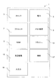
図1は、場合によってはシステムオンチップとしても知られている集積回路マイクロコントローラ1を示すものであって、抵抗・コンデンサ発振器を備えるか、および/または、チップ外の水晶発振器(図示せず)からの入力を受信するクロックロジック3と、電力管理回路5と、プロセッサ7(例えば、ARM社製Cortex‐M0)と、メモリ保護ロジック9と、RAM11と、不揮発性フラッシュメモリ13と、一つ以上の周辺機器15と、無線通信ロジック17と、入出力回路19と、を備えている。
FIG. 1 shows an
これらの構成要素は、従来の方法で、例えば、回線とバス(図示せず)を使って、相互接続されている。メモリ保護ロジック9は、プロセッサ7からRAM111とフラッシュメモリ13への命令を横取りするように位置付けられている。製品に取り付けられるとき、マイクロコントローラ1は、電源、無線アンテナ、水晶発振器、センサ、出力デバイスなどの多くの外部構成要素に接続することができる。
These components are interconnected in a conventional manner, for example, using lines and buses (not shown). The
図2は、マイクロコントローラ1を示しており、その上に、ARM社製Cortexマイクロコントローラソフトウェアインタフェース規格のような、任意選択のハードウェア抽象化層21が存在する。該構造は、ファームウェアモジュール23と、ドライバ25と、ソフトウェアアプリケーション27と、を含む。ドライバ25は、ソフトウェア・アプリケーション27専用のことがある。
FIG. 2 shows a
ファームウェアモジュール23は、多くの組込みソフトウェアブロックを含む二進数アプリケーションである。無線プロトコルブロック31は、一つ以上の無線プロトコルスタックを実装する。無線イベントマネージャ33は、無線通信ロジック17のためのアクセスのスケジュール化、およびイベントの多重化を提供する。ライブラリ35は、共有ハードウェア資源管理と、乱数生成、割り込みと優先度の設定、(例えば、周辺機器を起動・停止するための)電力管理、暗号化機能、等の機能を提供する。ファームウェアマネージャ37は、ファームウェアモジュールを有効化・無効化することと、無線プロトコルスタックを有効化・無効化することをサポートする。
ファームウェアモジュール23は、システムベクタテーブルを所有し、すべてのリセットに関して該プログラムに対する入口点となる。
The
ファームウェアモジュール23用のアプリケーションプログラミングインタフェース(API)29は、ソフトウェアアプリケーション27がファームウェアモジュール23内の関数を呼び出すことを可能にする。これは、全面的にシステム呼び出しを使用して実施される。ARM社製プロセッサを使用する場合、各API関数プロトタイプは、コンパイル時に、ファームウェアの機能が関係付けられたスーパーバイザ呼び出し(SVC)番号を介して該機能にマッピングされる。このマッピングが提供されることによって、ソフトウェアアプリケーション27の開発者は、関数を正しく呼び出すことができる。
An application programming interface (API) 29 for the
ファームウェアモジュール23は、イベントをソフトウェア割り込みとしてソフトウェアアプリケーション27に伝えることができ、その内容は、ソフトウェアアプリケーション27によって読み込まれる(ポーリングされる)までバッファに格納される。該読み込みは、API呼び出し(例えば、event_get())を通して行われる。
The
ソフトウェアアプリケーション27は、マイクロコントローラ1のハードウェアを、ファームウェアモジュール23を利用して間接的に該ハードウェアを使用することができることに加えて、直接またはハードウェア抽象化層21を介し、例えば、アプリケーション固有のドライバ25を用いて、アクセスすることができる。
In addition to being able to use the hardware of the
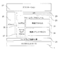
図3は、RAM11とフラッシュ13がファームウェアモジュール23と(任意のアプリケーション固有のドライバ25を含む)ソフトウェアアプリケーション27とでどのように共有されるのかを示している。ARM社製Cortex‐M0プロセッサ7を使用する場合、フラッシュ13は、アドレスがゼロ(0x0000 0000)から上に向かって、その容量である、プログラムメモリサイズまで割り当てられ、RAM11は、アドレスが0x2000 0000から上に向かって、(0x2000 0000+RAMサイズ)まで割り当てられる。異なるタイプのプロセッサを使用する場合、別のアドレス値を使用することもある。
FIG. 3 shows how the
フラッシュ13は、アドレスCLENR0(領域0のプログラムの長さ)の両側に二つの異なる領域を含む。ゼロとCLENR0の間にある領域0は、ファームウェアモジュール23がロードされる場所である。その割り込みベクタテーブルは、アドレスのゼロに格納されている。CLENR0から上方に延びる領域1は、ソフトウェアアプリケーション27がロードされる場所である。それも、アドレスCLENR0に割り込みベクタテーブルを有するが、割り込みベクタテーブルの目的は、以下で説明する。なお、デバイス1は、設定情報やフラグを格納するなどといった他の目的のために使用される不揮発性メモリ(図示せず)を別に有することがある。
The
RAM11も同様に、基底アドレス0x2000 0000からRLENR0までの領域0とRLENR0から上方に延びる領域1を有する。RAMの領域0は、ファームウェアモジュール23のためのデータ記憶域を提供し、RAMの領域1は、ソフトウェアアプリケーション27のためのデータ記憶域を提供する。呼び出しスタックは、ファームウェアモジュール23とソフトウェアアプリケーション27とで共有され、例えば、0x2000 0000+RAMサイズから下方に拡がる。呼び出しスタックに割り当てられるメモリは、ソフトウェアアプリケーション27とファームウェアモジュール23の両方の必要性に十分に応える大きさでなければならない。
Similarly, the
ファームウェアモジュール23による呼び出しスタックの必要使用量は、デバイス1に関して、チップメーカーによって公開されることがある。したがって、ソフトウェアアプリケーション27の開発者は、初期スタックポインタを定めて、ファームウェアモジュール23と自分のソフトウェアアプリケーション27の両方にとって十分なスタックメモリを予約する必要がある。ファームウェアモジュール23は、リセット時にメインスタックポインタを初期化することになる。
The required usage of the call stack by the
メモリ保護ロジック9は、プロセッサ7からフラッシュ13およびRAM11に対するすべてのメモリアクセス要求(例えば、読み取り要求)を横取りするように構成される。該ロジックは、アクセス要求命令の発行元(例えば、該要求は、ファームウェアモジュール23からのものであるか、またはソフトウェアアプリケーション27からのものであるか)を決定する。また、様々な発行元に対してそれぞれのアクセス権限を指定する(例えば、一つ以上の専用レジスタに格納された)メモリ保護構成データにアクセスし、それに応じてアクセス要求を許可または拒否する。
The
本発明のいくつかの好ましい実施形態では、ソフトウェアアプリケーション27は、フラッシュの領域0とRAMの領域0に対する読み取りおよび/または書き込みのアクセスを拒否される。こうすれば、ファームウェアモジュール23の機密性を保護し、また、ソフトウェアアプリケーション27によって、ファームウェアモジュール23に割り当てられたメモリ箇所に対し、不注意なまたは悪意のある書き込みが行なわれることを防止することができ、それによって堅牢性および安全性を向上させることができる。フラッシュのソフトウェアアプリケーション領域1も、例えば、外部デバッグインタフェースを介したリードバック行為から保護するなど、読み取りアクセスから保護することができる。
In some preferred embodiments of the present invention,
このことは、ソフトウェアアプリケーション27にはRAM領域0への書き込みアクセス権がないので、初期スタックポインタをRAM領域0におくことはできないことを意味する。本発明の他の実施形態では、呼び出しスタックは、二つの部分から成るものとし、ファームウェアモジュール23の呼び出しスタックはRAM領域0に置かれ、ソフトウェアアプリケーション27の呼び出しスタックはRAM領域1に置かれる。
This means that the initial stack pointer cannot be placed in the RAM area 0 because the
図4は、ARM社製Cortex‐M0プロセッサによって提供されて、矢印の方向に優先度が増加する、様々な割り込みレベル41と、これらのレベルが、ファームウェアモジュール23とソフトウェアアプリケーション27によって使用される割込みレベル43にどのようにマッピングされるかということと、を示している。
FIG. 4 shows the various interrupt
メインという背景の処理環境の上には、優先度の高くなる順に、ソフトウェアアプリケーション低優先度と、ファームウェアモジュール低優先度と、ソフトウェアアプリケーション高優先度と、ファームウェアモジュール高優先度として使用される四つの割り込み優先度がある。高優先度のソフトウェアアプリケーション割り込みは、短い待ち時間が要求される緊急割り込みに使用される。 On top of the main processing environment, there are four types of software applications that are used as high priority, software application low priority, firmware module low priority, software application high priority, and firmware module high priority. There is an interrupt priority. High priority software application interrupts are used for emergency interrupts that require a short latency.
図5は、優先度レベルが変化する可能性のある様々な例を示している。 FIG. 5 shows various examples in which the priority level may change.
図5(a)は、背景となるメイン処理が、低優先度のソフトウェアアプリケーション、例えば、シリアル用ドライバによって割り込みを受ける様子を示している。次いで、ソフトウェアアプリケーション27は、(スーパーバイザ呼び出し(SVC)例外を発生させることによって)ファームウェアモジュール23にAPI呼び出しを行なう。ファームウェアモジュール23は、該呼び出しをファームウェア低優先度レベルで処理した後に、アプリケーション低優先度レベルに戻る。最後に、ソフトウェアアプリケーション27は操作を完了し、メインという背景レベルに実行が戻る。
FIG. 5A shows a state in which the background main process is interrupted by a low-priority software application, for example, a serial driver. The
図5(b)は、ファームウェアモジュール23へAPI呼び出しが(SVC例外を発生させることによって)メインの処理環境から発生する様子を示している。ファームウェア低優先度で実行するAPI機能は、高優先度のソフトウェアアプリケーション例外によって割り込みされる。これは、例えば、センサ入力を処理することであるかもしれない。ソフトウェアアプリケーションが高優先度の実行を終了すると、ファームウェアのAPI呼び出しは、低優先度のレベルで処理を継続することができ、最終的に背景であるメイン処理に戻る。
FIG. 5B shows how an API call to the
図5(c)は、背景であるメイン処理がファームウェアモジュール23によって高優先度の割り込みを受けた様子を示している。これは、着信する無線パケットのような、無線イベントマネージャ33が応答しなければならない、緊急を要する無線通信割り込みが原因である可能性がある。ファームウェアモジュール23内の割り込みサービスルーチンは、低優先度のファームウェア例外フラグを設定して、無線プロトコルスタックのより高いレベルに通知する。高優先度のルーチンが完了すると、プロセッサ7のテールチェイン機能によって(つまり、途中で、背景であるメインのレベルに戻すことなく)、直ちに低優先度のルーチンが実行されている。今度は、低優先度のファームウェアルーチンが、例外フラグを設定して、無線データパケットが受信されたという信号をソフトウェアアプリケーション27に通知する。この例外は、低優先度のファームウェアモジュールルーチンの完了後に直ちに実行される。この例では、ソフトウェアアプリケーション27は、次に、SVCを介してファームウェアモジュール23にAPI呼び出しを行ない、完了後に、処理環境をSVCからソフトウェアアプリケーション27に戻す。最後に、ソフトウェアアプリケーション低優先度操作が完了し、メインのレベルに実行が戻る。
FIG. 5C shows a state in which the main process as a background has received a high priority interrupt by the
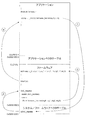
図6〜図8は、ソフトウェアアプリケーション27とファームウェアモジュール23との間でどのように制御が渡されるのかを例を用いて説明している。説明のために、未コンパイルのC言語コードを抽出したものが使用されている。もちろん、実際には、プロセッサ7によってフラッシュメモリ13からの二進数命令が実行される。番号の付いた矢印は、連続する実行ステップを示している。
6 to 8 illustrate an example of how control is passed between the
図6は、ソフトウェアアプリケーション27がファームウェアモジュール23のAPI29を通して機能を呼び出す様子を示している。アプリケーション27は、チップメーカーによってソフトウェアアプリケーション開発者に供給されたファームウェアヘッダファイルを使用して、ファームウェアのAPI29から取り込まれたプロトタイプを使ってある関数を呼び出す。_SVC(x) プラグマは、該関数がソフトウェアアプリケーション23によって呼び出されると、スーパーバイザ呼び出し(SVC)例外を発生させる命令を、コンパイラがオブジェクトコード中に挿入する。
FIG. 6 shows how the
プロセッサ7は、(システム割り込みベクタテーブルとして機能する)ファームウェアモジュールの割り込みベクタテーブルを介して、SVC処理機能を起動する。ソフトウェアアプリケーション27によって呼び出される関数と関係付けられたSVC番号は、引数と一緒に、SVC処理機能に渡される。このような引数は、プロセッサによって、レジスタを介して、または、コールスタックを介して渡すことができる。SVC処理機能は、SVC番号を使用して正しいファームウェアモジュールの関数を呼び出す。これは、無線制御機能(例えば、無線でデータを送信する命令)、または(例えば、ファームウェアモジュールを無効化する)ファームウェア管理機能、または(例えば、乱数を生成する)ライブラリ関数、であってもよい。関数が実行されると、ソフトウェアアプリケーション27に戻る。戻り値が、レジスタ内またはコールスタック上で利用可能であるようにできる。
The
図7は、ソフトウェアアプリケーション27がシステム呼び出しを介して、自分自身の機能の一つを呼び出す様子を示している。実行レベルを低優先度から高優先度に変更するために、このようなことを行なう可能性がある。図6における状況と同様に、ソフトウェアアプリケーション27は、ファームウェアモジュール27にあるSVC処理機能に実行が渡されるようにSVCを発生させる。しかしながら、この場合、該命令は、ソフトウェアアプリケーション自身の使用のために予約されている範囲にあるSVC番号を使用する。このようにして、ファームウェアモジュール23は、おそらくそれまでの動作とは異なる優先度レベルで、ソフトウェアアプリケーション27内の処理関数(app_systemcall_function())に実行が分岐するようにする。
FIG. 7 shows how the
図8は、ハードウェア割り込みをソフトウェアアプリケーション27がどのようにして受け取るのかを示している。ファームウェアモジュール23は、ファームウェアモジュール23が処理するように構成されている割り込みでない限り、初期設定ではソフトウェアアプリケーション27に割り込みを転送するように設定されている。さらに、ファームウェアモジュール23が(例えば、ファームウェアマネージャ37への適切なAPI呼び出しを介して)ソフトウェアアプリケーション27によって無効にされている場合、ファームウェアモジュールは、全ての割り込みをソフトウェアアプリケーション27に転送する。
FIG. 8 shows how the
モーションセンサなどから割り込みを受信すると、ファームウェアモジュール23の割り込み処理機能に制御が渡される。この処理機能は、ファームウェアモジュール23が有効になっているかどうか、そして、ファームウェアモジュール23が対処するように設定されている割り込みかであるかどうかを調べる。もしそうであれば、ファームウェアモジュール23は、割り込みを処理する。そうでない場合は、ソフトウェアアプリケーション27の割り込み処理ルーチンに実行を分岐させる。ファームウェアモジュール23は、ソフトウェアアプリケーションベクタテーブルの(CLENR0という)位置が予め決められていて、このベクタテーブルでの相対位置がファームウェアモジュールのベクタテーブルでの相対位置と同じなので、このルーチンがどこにあるのかを知ることができる。
When an interrupt is received from a motion sensor or the like, control is passed to the interrupt processing function of the
このようにして、集積回路無線通信チップのファームウェアメモリアドレスにプログラムされた、無線制御ロジックを実施するファームウェアモジュールを、安全かつ便利に構成・使用することができる。 In this way, the firmware module that implements the wireless control logic programmed into the firmware memory address of the integrated circuit wireless communication chip can be configured and used safely and conveniently.
Claims (31)
前記デバイスは、プロセッサと、メモリと、無線通信ロジックと、を備え、
前記メモリには、所定の無線プロトコルに従って前記無線通信ロジックを制御するための命令を含むソフトウェアファームウェアモジュールがファームウェアメモリアドレスに格納され、
前記プロセッサは、各々にスーパーバイザ呼び出し番号が関係付けられたスーパーバイザ呼び出し命令を受信し、(i)前記ソフトウェアファームウェアモジュールのスーパーバイザ呼び出し処理部を起動して、(ii)前記呼び出し処理部が前記スーパーバイザ呼び出し番号を利用できるようにすることによって、スーパーバイザ呼び出し命令に応答するように構成され、
前記方法は、所定のアプリケーションメモリアドレスに格納されるようにソフトウェアアプリケーションを前記デバイスの前記メモリ内に読み込むことを含み、
前記ソフトウェアアプリケーションは、起動すべき無線通信機能に対応する所定のスーパーバイザ呼び出し番号が関係付けられたスーパーバイザ呼び出し命令を前記プロセッサに発行することによって、前記ソフトウェアファームウェアモジュールから前記無線通信機能を起動するように設定される
ことを特徴とする、集積回路型無線通信デバイスを構成する方法。 A method of configuring an integrated circuit type wireless communication device comprising:
The device comprises a processor, memory, and wireless communication logic,
In the memory, a software firmware module including instructions for controlling the wireless communication logic according to a predetermined wireless protocol is stored in a firmware memory address,
The processor receives the supervisor call instruction to the supervisor call number is associated to each, (i) Start the supervisor call processing portion of the software firmware module, (ii) the call processing unit is the supervisor Configured to respond to supervisor call instructions by making the call number available,
The method includes loading a software application into the memory of the device to be stored at a predetermined application memory address;
Said software application by issuing a supervisor call instruction in which a predetermined supervisor call number corresponding to the start all-out wireless communication function is associated with the processor, activating the wireless communication function from the software firmware module A method of configuring an integrated circuit type wireless communication device, characterized in that:
ソフトウェアアプリケーションを、所定のアプリケーションのメモリアドレスに格納されるように、前記デバイスの前記メモリに読み込むことと、
所定の無線プロトコルに従って前記無線通信ロジックを制御するための命令を含むソフトウェアファームウェアモジュールを、所定のファームウェアメモリアドレスに格納されるように、前記デバイスの前記メモリに読み込むことと、を含み、
前記プロセッサは、各々にスーパーバイザ呼び出し番号が関係付けられたスーパーバイザ呼び出し命令を受信し、(i)前記ソフトウェアファームウェアモジュールのスーパーバイザ呼び出し処理部を起動して、(ii)前記呼び出し処理部が前記スーパーバイザ呼び出し番号を利用できるようにすることによって、スーパーバイザ呼び出し命令に応答するように構成され、
前記ソフトウェアアプリケーションは、起動すべき無線通信機能に対応する所定のスーパーバイザ呼び出し番号が関係付けられたスーパーバイザ呼び出し命令を前記プロセッサに発行することによって、前記ソフトウェアファームウェアモジュールから前記無線通信機能を起動するように設定される
ことを特徴とする、集積回路型無線通信デバイスを構成する方法。 A method of configuring an integrated circuit type wireless communication device comprising a processor, a memory, and wireless communication logic, the method comprising:
Loading a software application into the memory of the device to be stored at a memory address of a predetermined application;
Loading a software firmware module including instructions for controlling the wireless communication logic in accordance with a predetermined wireless protocol into the memory of the device to be stored at a predetermined firmware memory address;
The processor receives the supervisor call instruction to the supervisor call number is associated to each, (i) Start the supervisor call processing portion of the software firmware module, (ii) the call processing unit is the supervisor Configured to respond to supervisor call instructions by making the call number available,
Said software application by issuing a supervisor call instruction in which a predetermined supervisor call number corresponding to the start all-out wireless communication function is associated with the processor, activating the wireless communication function from the software firmware module A method of configuring an integrated circuit type wireless communication device, characterized in that:
ことを特徴とする、請求項1または2に記載の方法。 The method of claim 1 or 2, wherein the software firmware module is a linked binary module.
ことを特徴とする、請求項1乃至請求項3のいずれかに記載の方法。 The software firmware module is configured such that all wireless communication functions provided by the software firmware module are activated by supervisor call instructions having respective supervisor call numbers according to a predetermined correspondence between the numbers and functions. The method according to claim 1, wherein the method is set.
前記ソフトウェアアプリケーションをコンパイルすることと、
前記コンパイルするときに、スーパーバイザ呼び出し番号と無線通信機能との対応関係を用いることと、を含む
ことを特徴とする、請求項1乃至請求項4のいずれかに記載の方法。 The method further comprises:
Compiling the software application;
The method according to claim 1, comprising using a correspondence relationship between a supervisor call number and a wireless communication function when compiling.
前記ソフトウェアアプリケーションをコンパイルしたり読み込んだりするときに、前記所定のソフトウェアアプリケーションメモリアドレスを利用することを含む
ことを特徴とする、請求項1乃至請求項5のいずれかに記載の方法。 The method further comprises:
6. A method according to any one of the preceding claims, comprising using the predetermined software application memory address when compiling or loading the software application.
ことを特徴とする、請求項1乃至請求項6のいずれかに記載の方法。 The method according to any one of claims 1 to 6, wherein the software application is configured to issue a supervisor call instruction by executing a dedicated SVC processor instruction.
ことを特徴とする、請求項1乃至請求項7のいずれかに記載の方法。 The software firmware module and the software application each have an interrupt vector table, and the device is configured to use the vector table of the software firmware module when handling an interrupt, the software firmware module 8. A method according to any one of claims 1 to 7, characterized in that all interrupts that are not programmed to be handled are set to be passed to the software application.
ことを特徴とする、請求項8に記載の方法。 9. The method of claim 8, wherein the software firmware module and the interrupt vector table of the software application use the same relative interrupt vector address position.
ことを特徴とする、請求項1乃至請求項9のいずれかに記載の方法。 The device comprises memory protection logic arranged to intercept memory access instructions and configured to prevent the software application from reading or overwriting the software firmware module. A method according to any one of claims 1 to 9.
前記デバイスは、プロセッサと、メモリと、無線通信ロジックと、を備え、
前記メモリには、所定の無線プロトコルに従って前記無線通信ロジックを制御するための命令を含むソフトウェアファームウェアモジュールがファームウェアメモリアドレスに格納され、
前記プロセッサは、各々にスーパーバイザ呼び出し番号が関係付けられたスーパーバイザ呼び出し命令を受信し、(i)前記ソフトウェアファームウェアモジュールのスーパーバイザ呼び出し処理部を起動して、(ii)前記呼び出し処理部が前記スーパーバイザ呼び出し番号を利用できるようにすることによって、スーパーバイザ呼び出し命令に応答するように構成され、
前記メモリには、前記ソフトウェアファームウェアモジュールから無線通信機能を、起動すべき前記無線通信機能に対応する所定のスーパーバイザ呼び出し番号が関係付けられたスーパーバイザ呼び出し命令を前記プロセッサに発行することによって、前記ソフトウェアファームウェアモジュールから前記無線通信機能を起動するように設定されるソフトウェアアプリケーションが、所定のアプリケーションメモリアドレスに格納される
ことを特徴とする、集積回路型無線通信デバイス。 An integrated circuit type wireless communication device,
The device comprises a processor, memory, and wireless communication logic,
In the memory, a software firmware module including instructions for controlling the wireless communication logic according to a predetermined wireless protocol is stored in a firmware memory address,
The processor receives the supervisor call instruction to the supervisor call number is associated to each, (i) Start the supervisor call processing portion of the software firmware module, (ii) the call processing unit is the supervisor Configured to respond to supervisor call instructions by making the call number available,
In the memory by issuing a wireless communication function from the software firmware module, a supervisor call instruction in which a predetermined supervisor call number is associated corresponding to the wireless communication function to be activated to the processor, the software firmware An integrated circuit type wireless communication device, wherein a software application set to activate the wireless communication function from a module is stored in a predetermined application memory address.
ことを特徴とする、請求項11に記載のデバイス。 The software firmware module is configured such that all wireless communication functions provided by the software firmware module are activated by supervisor call instructions having respective supervisor call numbers according to a predetermined correspondence between the numbers and functions. The device according to claim 11, wherein the device is set.
ことを特徴とする、請求項11または12に記載のデバイス。 The software firmware module is configured such that all functions provided by the software firmware module are activated by issuing the supervisor call instruction. device.
ことを特徴とする、請求項11乃至請求項13のいずれかに記載のデバイス。 14. A device according to any of claims 11 to 13, wherein a runtime link is not required when executing the software application on the device.
ことを特徴とする、請求項11乃至請求項14のいずれかに記載のデバイス。 15. A device according to any of claims 11 to 14, wherein the software application is configured to issue supervisor call instructions by executing dedicated SVC processor instructions.
ことを特徴とする、請求項11乃至請求項15のいずれかに記載のデバイス。 The processor and / or the software application, wherein the configured values of one or more arguments available to the supervisor call processing unit, according to any one of claims 11 to 15 Devices.
ことを特徴とする、請求項11乃至請求項16のいずれかに記載のデバイス。 The processor is configured to handle supervisor call instructions from the software application as exceptions, the processor supports multiple interrupt priorities, and some functions of the software firmware module are relatively high priority 17. A device according to any of claims 11 to 16, characterized in that a degree is assigned and other functions of the software firmware module are assigned a relatively low priority.
ことを特徴とする、請求項17に記載のデバイス。 The software application is configured to handle interrupts with a relatively high priority for some event-driven functions and a relatively low priority for other event-driven functions. The device according to claim 17, characterized in that:
ことを特徴とする、請求項18に記載のデバイス。 The device of claim 18, wherein the high priority and low priority of the software application are interleaved with the high priority and low priority of the firmware module.
ことを特徴とする、請求項18または請求項19に記載のデバイス。 20. Device according to claim 18 or 19, characterized in that the highest priority level of the firmware is higher than the highest priority level of the software application.
ことを特徴とする、請求項11乃至請求項20のいずれかに記載のデバイス。 The device according to any one of claims 11 to 20, wherein the software firmware module is configured to activate a function of the software application upon receiving an interrupt.
ことを特徴とする、請求項11乃至請求項21のいずれかに記載のデバイス。 The software firmware module and the software application each have an interrupt vector table, and the device is configured to use the vector table of the software firmware module when handling an interrupt, the software firmware module 22. A device according to any of claims 11 to 21, characterized in that it is set to pass all interrupts not programmed to be processed to the software application.
ことを特徴とする、請求項22に記載のデバイス。 The device of claim 22, wherein the software firmware module and the interrupt vector table of the software application use the same relative interrupt vector address position.
ことを特徴とする、請求項11乃至請求項23のいずれかに記載のデバイス。 Wherein the software firmware module, via a call to the software firmware module, in order to return the resources to the software application, the software firmware module so as to disable all reset memory protection protocol stack, substantially 24. A device as claimed in any of claims 11 to 23, characterized in that upon being invalidated, the software firmware module forwards all interrupts to the software application.
ことを特徴とする、請求項11乃至請求項24のいずれかに記載のデバイス。 25. A device as claimed in any of claims 11 to 24, wherein the processor supports seamless transition from one interrupt priority level to another.
ことを特徴とする、請求項11乃至請求項25のいずれかに記載のデバイス。 The device is arranged to intercept memory access instructions and allows the software application to read or overwrite the software firmware module and / or to read or write RAM associated with the software firmware. 26. A device as claimed in any of claims 11 to 25, comprising memory protection logic configured to prevent.
ことを特徴とする、請求項11乃至請求項26のいずれかに記載のデバイス。 The memory is a non-volatile memory that supports random access reading, and the device is configured to execute the software firmware module and the software application directly from the non-volatile memory. 27. A device according to any one of claims 11 to 26.
ことを特徴とする、請求項11乃至請求項27のいずれかに記載のデバイス。 The software firmware module is a linked binary module and not linked to the software application;
A device according to any of claims 11 to 27, characterized in that
所定の無線プロトコルに従って前記無線通信ロジックを制御するための命令と、
ソフトウェアアプリケーションによって発行されるスーパーバイザ呼び出し命令に対し、前記スーパーバイザ呼び出し命令と関係付けられたスーパーバイザ呼び出し番号に対応する無線通信機能を実行することによって、応答するように設定されたスーパーバイザ呼び出し処理部と、を含む
ことを特徴とするソフトウェアファームウェアモジュール。 A software firmware module loaded into a firmware memory address on an integrated circuit type wireless communication device comprising a processor, a memory, and wireless communication logic, wherein the software firmware module is a linked binary module;
Instructions for controlling the wireless communication logic according to a predetermined wireless protocol;
To supervisor call instruction issued by the software application, by executing a wireless communication function corresponding to the supervisor call number associated with the supervisor call instruction, a supervisor call processing unit that is configured to respond, A software firmware module comprising:
ことを特徴とする、請求項29に記載のソフトウェアファームウェアモジュール。 30. Software firmware module according to claim 29, characterized in that it is a linked binary module.
ことを特徴とするソフトウェアアプリケーション。 A processor, a memory, a software application is loaded to a predetermined software application memory addresses on the integrated circuit type wireless communication device comprises a wireless communication logic, wherein the software application corresponding to the wireless communication function-out start all A plurality of instructions for activating the wireless communication function by issuing a supervisor call instruction associated with a predetermined supervisor call number to the processor ;
Software application that features and this.
Applications Claiming Priority (3)
| Application Number | Priority Date | Filing Date | Title |
|---|---|---|---|
| GB201211423A GB2503471B (en) | 2012-06-27 | 2012-06-27 | Integrated-circuit radio |
| GB1211423.7 | 2012-06-27 | ||
| PCT/GB2013/051692 WO2014001801A1 (en) | 2012-06-27 | 2013-06-26 | Integrated-circuit radio |
Publications (3)
| Publication Number | Publication Date |
|---|---|
| JP2015524964A JP2015524964A (en) | 2015-08-27 |
| JP2015524964A5 JP2015524964A5 (en) | 2016-08-12 |
| JP6326047B2 true JP6326047B2 (en) | 2018-05-16 |
Family
ID=46704313
Family Applications (1)
| Application Number | Title | Priority Date | Filing Date |
|---|---|---|---|
| JP2015519340A Active JP6326047B2 (en) | 2012-06-27 | 2013-06-26 | Integrated circuit radio |
Country Status (8)
| Country | Link |
|---|---|
| US (2) | US9317348B2 (en) |
| EP (1) | EP2867768A1 (en) |
| JP (1) | JP6326047B2 (en) |
| KR (1) | KR102088690B1 (en) |
| CN (1) | CN104412230B (en) |
| GB (1) | GB2503471B (en) |
| TW (1) | TWI603265B (en) |
| WO (1) | WO2014001801A1 (en) |
Families Citing this family (4)
| Publication number | Priority date | Publication date | Assignee | Title |
|---|---|---|---|---|
| GB2515364B (en) * | 2013-12-20 | 2015-06-17 | Nordic Semiconductor Asa | Updatable integrated-circuit radio |
| GB2521607B (en) * | 2013-12-23 | 2016-03-23 | Nordic Semiconductor Asa | Integrated-Circuit Radio |
| WO2020240235A1 (en) * | 2019-05-31 | 2020-12-03 | Micron Technology, Inc | Controller for a memory component |
| CN112203319B (en) * | 2020-10-23 | 2022-07-15 | 四川长虹网络科技有限责任公司 | Test method and device of ZigBee device, computer device and storage medium |
Family Cites Families (29)
| Publication number | Priority date | Publication date | Assignee | Title |
|---|---|---|---|---|
| DE3632139A1 (en) | 1986-09-22 | 1988-04-07 | Bbc Brown Boveri & Cie | Method of executing two programs which are written in different programming languages |
| JPS63296140A (en) * | 1987-05-28 | 1988-12-02 | Canon Inc | Interruption control system |
| US5161228A (en) * | 1988-03-02 | 1992-11-03 | Ricoh Company, Ltd. | System with selectively exclusionary enablement for plural indirect address type interrupt control circuit |
| JPH07105124A (en) * | 1993-10-06 | 1995-04-21 | Toshiba Corp | Interruption controller |
| CA2143488C (en) * | 1995-02-27 | 2000-01-11 | Robert Paul Duncan | Dynamic link libraries without linker or loader support |
| US6223275B1 (en) * | 1997-06-20 | 2001-04-24 | Sony Corporation | Microprocessor with reduced instruction set limiting the address space to upper 2 Mbytes and executing a long type register branch instruction in three intermediate instructions |
| US20020073398A1 (en) * | 1998-12-14 | 2002-06-13 | Jeffrey L. Tinker | Method and system for modifying executable code to add additional functionality |
| JP2002108625A (en) * | 2000-09-26 | 2002-04-12 | Toshiba Corp | Language processor and recording medium in which language processing program is stored |
| US7237121B2 (en) | 2001-09-17 | 2007-06-26 | Texas Instruments Incorporated | Secure bootloader for securing digital devices |
| US6874069B2 (en) | 2002-07-26 | 2005-03-29 | Silicon Storage Technology, Inc. | Microcontroller having an embedded non-volatile memory array with read protection for the array or portions thereof |
| US7120794B2 (en) * | 2003-10-29 | 2006-10-10 | Qualcomm Inc. | System for invoking a privileged function in a device |
| US7206884B2 (en) * | 2004-02-11 | 2007-04-17 | Arm Limited | Interrupt priority control within a nested interrupt system |
| US7318150B2 (en) * | 2004-02-25 | 2008-01-08 | Intel Corporation | System and method to support platform firmware as a trusted process |
| JP2005242806A (en) * | 2004-02-27 | 2005-09-08 | Renesas Technology Corp | Data processor |
| US7647589B1 (en) * | 2005-02-07 | 2010-01-12 | Parallels Software International, Inc. | Methods and systems for safe execution of guest code in virtual machine context |
| US20070112680A1 (en) * | 2005-11-11 | 2007-05-17 | Infineon Technologies Ag | System and method for processing digital media content in a mobile device |
| EP1980032B1 (en) * | 2005-12-07 | 2016-03-09 | Freescale Semiconductor, Inc. | Wireless subscriber communication unit and method of power control with back-off therefor |
| FR2905819B1 (en) * | 2006-09-12 | 2013-01-18 | Wavecom | METHOD FOR MANAGING THE SOFTWARE ARCHITECTURE OF A RADIO COMMUNICATION CIRCUIT, APPLICATION, CORRESPONDING COMPUTER PROGRAM PRODUCT AND CIRCUIT. |
| US20090096586A1 (en) * | 2007-10-12 | 2009-04-16 | Icontrol, Inc. | Radiofrequency Tracking and Communication Device and Method for Operating the Same |
| US20090253384A1 (en) * | 2008-04-04 | 2009-10-08 | Stmicroelectronics, Ltd. | Dual Mode Radio Frequency Front End Circuit |
| US8291202B2 (en) * | 2008-08-08 | 2012-10-16 | Qualcomm Incorporated | Apparatus and methods for speculative interrupt vector prefetching |
| US8143699B2 (en) * | 2009-02-25 | 2012-03-27 | Taiwan Semiconductor Manufacturing Co., Ltd. | Dual-dielectric MIM capacitors for system-on-chip applications |
| US20110117956A1 (en) * | 2009-11-17 | 2011-05-19 | Yosi Levi | Industrial radio device with unified programming interface and methods |
| US8862178B2 (en) * | 2010-02-24 | 2014-10-14 | Qualcomm Incorporated | Methods and systems for managing participation in multiple wireless networks |
| US20120255031A1 (en) * | 2011-03-28 | 2012-10-04 | Mcafee, Inc. | System and method for securing memory using below-operating system trapping |
| US9063847B2 (en) * | 2011-04-19 | 2015-06-23 | Dell Products, Lp | System and method for managing space allocation within a file system |
| US9563410B2 (en) * | 2011-05-25 | 2017-02-07 | Amx Llc | Data-driven menuing system for providing a flexible user interface on an electronic device |
| US10185566B2 (en) * | 2012-04-27 | 2019-01-22 | Intel Corporation | Migrating tasks between asymmetric computing elements of a multi-core processor |
| US20130338848A1 (en) * | 2012-06-19 | 2013-12-19 | Scott Park | Method and Apparatus for Leveling Recreational Vehicles |
-
2012
- 2012-06-27 GB GB201211423A patent/GB2503471B/en active Active
-
2013
- 2013-06-21 US US13/924,160 patent/US9317348B2/en active Active
- 2013-06-24 TW TW102122333A patent/TWI603265B/en active
- 2013-06-26 EP EP13733435.5A patent/EP2867768A1/en active Pending
- 2013-06-26 WO PCT/GB2013/051692 patent/WO2014001801A1/en active Application Filing
- 2013-06-26 CN CN201380034634.2A patent/CN104412230B/en active Active
- 2013-06-26 JP JP2015519340A patent/JP6326047B2/en active Active
- 2013-06-26 KR KR1020157002104A patent/KR102088690B1/en active IP Right Grant
-
2016
- 2016-03-11 US US15/068,046 patent/US20160196170A1/en not_active Abandoned
Also Published As
| Publication number | Publication date |
|---|---|
| US9317348B2 (en) | 2016-04-19 |
| WO2014001801A1 (en) | 2014-01-03 |
| KR102088690B1 (en) | 2020-03-16 |
| JP2015524964A (en) | 2015-08-27 |
| KR20150024927A (en) | 2015-03-09 |
| GB2503471A (en) | 2014-01-01 |
| US20160196170A1 (en) | 2016-07-07 |
| GB201211423D0 (en) | 2012-08-08 |
| CN104412230B (en) | 2018-06-22 |
| EP2867768A1 (en) | 2015-05-06 |
| TW201401169A (en) | 2014-01-01 |
| CN104412230A (en) | 2015-03-11 |
| US20140007141A1 (en) | 2014-01-02 |
| GB2503471B (en) | 2015-05-06 |
| TWI603265B (en) | 2017-10-21 |
Similar Documents
| Publication | Publication Date | Title |
|---|---|---|
| JP6306578B2 (en) | Memory protection device and protection method | |
| US8392895B2 (en) | Firmware extension method and firmware builder | |
| US20130305259A1 (en) | Hardware control method and apparatus | |
| JP2007206885A (en) | Computer system and system starting method | |
| JP6326047B2 (en) | Integrated circuit radio | |
| US9891908B2 (en) | Updatable integrated-circuit radio | |
| JP5307133B2 (en) | Device emulation support apparatus, device emulation support method, device emulation support circuit, and information processing apparatus | |
| JP5622429B2 (en) | Microcomputer | |
| JP6495290B2 (en) | IC wireless device | |
| CN106922189B (en) | Equipment agent device and control method thereof | |
| Bulusu | Asymmetric multiprocessing real time operating system on multicore platforms | |
| JP2011150457A (en) | Information processing apparatus and memory access control method | |
| JP2004252508A (en) | Method for converting software program for single processor into software program for multiprocessor | |
| Dibble et al. | Programming embedded systems: interacting with the embedded platform | |
| Levy | A Secure Operating System for the Internet of Things | |
| CN116048827A (en) | Inter-process function calling method and related equipment |
Legal Events
| Date | Code | Title | Description |
|---|---|---|---|
| A521 | Request for written amendment filed |
Free format text: JAPANESE INTERMEDIATE CODE: A523 Effective date: 20160624 |
|
| A621 | Written request for application examination |
Free format text: JAPANESE INTERMEDIATE CODE: A621 Effective date: 20160624 |
|
| A131 | Notification of reasons for refusal |
Free format text: JAPANESE INTERMEDIATE CODE: A131 Effective date: 20170627 |
|
| A601 | Written request for extension of time |
Free format text: JAPANESE INTERMEDIATE CODE: A601 Effective date: 20170925 |
|
| A521 | Request for written amendment filed |
Free format text: JAPANESE INTERMEDIATE CODE: A523 Effective date: 20171127 |
|
| TRDD | Decision of grant or rejection written | ||
| A01 | Written decision to grant a patent or to grant a registration (utility model) |
Free format text: JAPANESE INTERMEDIATE CODE: A01 Effective date: 20180320 |
|
| A61 | First payment of annual fees (during grant procedure) |
Free format text: JAPANESE INTERMEDIATE CODE: A61 Effective date: 20180413 |
|
| R150 | Certificate of patent or registration of utility model |
Ref document number: 6326047 Country of ref document: JP Free format text: JAPANESE INTERMEDIATE CODE: R150 |
|
| R250 | Receipt of annual fees |
Free format text: JAPANESE INTERMEDIATE CODE: R250 |
|
| R250 | Receipt of annual fees |
Free format text: JAPANESE INTERMEDIATE CODE: R250 |
|
| R250 | Receipt of annual fees |
Free format text: JAPANESE INTERMEDIATE CODE: R250 |
|
| R250 | Receipt of annual fees |
Free format text: JAPANESE INTERMEDIATE CODE: R250 |