JP6324311B2 - Light guide plate, light source device, light guide plate manufacturing apparatus, and light guide plate manufacturing method - Google Patents
Light guide plate, light source device, light guide plate manufacturing apparatus, and light guide plate manufacturing method Download PDFInfo
- Publication number
- JP6324311B2 JP6324311B2 JP2014526896A JP2014526896A JP6324311B2 JP 6324311 B2 JP6324311 B2 JP 6324311B2 JP 2014526896 A JP2014526896 A JP 2014526896A JP 2014526896 A JP2014526896 A JP 2014526896A JP 6324311 B2 JP6324311 B2 JP 6324311B2
- Authority
- JP
- Japan
- Prior art keywords
- light guide
- layer
- guide plate
- roll
- printing unit
- Prior art date
- Legal status (The legal status is an assumption and is not a legal conclusion. Google has not performed a legal analysis and makes no representation as to the accuracy of the status listed.)
- Expired - Fee Related
Links
- 238000004519 manufacturing process Methods 0.000 title claims description 100
- 238000007639 printing Methods 0.000 claims description 107
- 238000009792 diffusion process Methods 0.000 claims description 73
- 239000000463 material Substances 0.000 claims description 23
- 238000000034 method Methods 0.000 claims description 7
- 238000002360 preparation method Methods 0.000 claims description 2
- 238000010586 diagram Methods 0.000 description 23
- 230000032258 transport Effects 0.000 description 12
- 239000004973 liquid crystal related substance Substances 0.000 description 7
- 238000007645 offset printing Methods 0.000 description 6
- 239000004925 Acrylic resin Substances 0.000 description 5
- 229920000178 Acrylic resin Polymers 0.000 description 5
- 229910052751 metal Inorganic materials 0.000 description 5
- 239000002184 metal Substances 0.000 description 5
- 238000001035 drying Methods 0.000 description 4
- 230000001771 impaired effect Effects 0.000 description 4
- 239000011347 resin Substances 0.000 description 4
- 229920005989 resin Polymers 0.000 description 4
- NIXOWILDQLNWCW-UHFFFAOYSA-N acrylic acid group Chemical group C(C=C)(=O)O NIXOWILDQLNWCW-UHFFFAOYSA-N 0.000 description 3
- 229920003229 poly(methyl methacrylate) Polymers 0.000 description 3
- 239000004926 polymethyl methacrylate Substances 0.000 description 3
- XEEYBQQBJWHFJM-UHFFFAOYSA-N Iron Chemical compound [Fe] XEEYBQQBJWHFJM-UHFFFAOYSA-N 0.000 description 2
- 239000011324 bead Substances 0.000 description 2
- 230000007423 decrease Effects 0.000 description 2
- 239000011521 glass Substances 0.000 description 2
- 230000001902 propagating effect Effects 0.000 description 2
- VYPSYNLAJGMNEJ-UHFFFAOYSA-N Silicium dioxide Chemical compound O=[Si]=O VYPSYNLAJGMNEJ-UHFFFAOYSA-N 0.000 description 1
- GWEVSGVZZGPLCZ-UHFFFAOYSA-N Titan oxide Chemical compound O=[Ti]=O GWEVSGVZZGPLCZ-UHFFFAOYSA-N 0.000 description 1
- 229910052782 aluminium Inorganic materials 0.000 description 1
- XAGFODPZIPBFFR-UHFFFAOYSA-N aluminium Chemical compound [Al] XAGFODPZIPBFFR-UHFFFAOYSA-N 0.000 description 1
- 125000003118 aryl group Chemical group 0.000 description 1
- 230000002238 attenuated effect Effects 0.000 description 1
- 239000000470 constituent Substances 0.000 description 1
- 229920001971 elastomer Polymers 0.000 description 1
- 238000005286 illumination Methods 0.000 description 1
- 229910052742 iron Inorganic materials 0.000 description 1
- 230000003287 optical effect Effects 0.000 description 1
- 239000002245 particle Substances 0.000 description 1
- 230000002093 peripheral effect Effects 0.000 description 1
- 238000007747 plating Methods 0.000 description 1
- 229920001225 polyester resin Polymers 0.000 description 1
- 239000004645 polyester resin Substances 0.000 description 1
- 229920001721 polyimide Polymers 0.000 description 1
- 239000009719 polyimide resin Substances 0.000 description 1
- 238000002310 reflectometry Methods 0.000 description 1
- 229920002379 silicone rubber Polymers 0.000 description 1
- 239000004945 silicone rubber Substances 0.000 description 1
- OGIDPMRJRNCKJF-UHFFFAOYSA-N titanium oxide Inorganic materials [Ti]=O OGIDPMRJRNCKJF-UHFFFAOYSA-N 0.000 description 1
Images

Classifications
-
- G—PHYSICS
- G02—OPTICS
- G02B—OPTICAL ELEMENTS, SYSTEMS OR APPARATUS
- G02B6/00—Light guides; Structural details of arrangements comprising light guides and other optical elements, e.g. couplings
- G02B6/0001—Light guides; Structural details of arrangements comprising light guides and other optical elements, e.g. couplings specially adapted for lighting devices or systems
- G02B6/0011—Light guides; Structural details of arrangements comprising light guides and other optical elements, e.g. couplings specially adapted for lighting devices or systems the light guides being planar or of plate-like form
- G02B6/0013—Means for improving the coupling-in of light from the light source into the light guide
- G02B6/0023—Means for improving the coupling-in of light from the light source into the light guide provided by one optical element, or plurality thereof, placed between the light guide and the light source, or around the light source
- G02B6/0025—Diffusing sheet or layer; Prismatic sheet or layer
-
- G—PHYSICS
- G02—OPTICS
- G02B—OPTICAL ELEMENTS, SYSTEMS OR APPARATUS
- G02B6/00—Light guides; Structural details of arrangements comprising light guides and other optical elements, e.g. couplings
- G02B6/0001—Light guides; Structural details of arrangements comprising light guides and other optical elements, e.g. couplings specially adapted for lighting devices or systems
- G02B6/0011—Light guides; Structural details of arrangements comprising light guides and other optical elements, e.g. couplings specially adapted for lighting devices or systems the light guides being planar or of plate-like form
- G02B6/0033—Means for improving the coupling-out of light from the light guide
- G02B6/0035—Means for improving the coupling-out of light from the light guide provided on the surface of the light guide or in the bulk of it
- G02B6/0036—2-D arrangement of prisms, protrusions, indentations or roughened surfaces
-
- F—MECHANICAL ENGINEERING; LIGHTING; HEATING; WEAPONS; BLASTING
- F21—LIGHTING
- F21K—NON-ELECTRIC LIGHT SOURCES USING LUMINESCENCE; LIGHT SOURCES USING ELECTROCHEMILUMINESCENCE; LIGHT SOURCES USING CHARGES OF COMBUSTIBLE MATERIAL; LIGHT SOURCES USING SEMICONDUCTOR DEVICES AS LIGHT-GENERATING ELEMENTS; LIGHT SOURCES NOT OTHERWISE PROVIDED FOR
- F21K9/00—Light sources using semiconductor devices as light-generating elements, e.g. using light-emitting diodes [LED] or lasers
-
- G—PHYSICS
- G02—OPTICS
- G02B—OPTICAL ELEMENTS, SYSTEMS OR APPARATUS
- G02B6/00—Light guides; Structural details of arrangements comprising light guides and other optical elements, e.g. couplings
- G02B6/0001—Light guides; Structural details of arrangements comprising light guides and other optical elements, e.g. couplings specially adapted for lighting devices or systems
- G02B6/0011—Light guides; Structural details of arrangements comprising light guides and other optical elements, e.g. couplings specially adapted for lighting devices or systems the light guides being planar or of plate-like form
- G02B6/0033—Means for improving the coupling-out of light from the light guide
- G02B6/005—Means for improving the coupling-out of light from the light guide provided by one optical element, or plurality thereof, placed on the light output side of the light guide
- G02B6/0051—Diffusing sheet or layer
-
- G—PHYSICS
- G02—OPTICS
- G02B—OPTICAL ELEMENTS, SYSTEMS OR APPARATUS
- G02B6/00—Light guides; Structural details of arrangements comprising light guides and other optical elements, e.g. couplings
- G02B6/0001—Light guides; Structural details of arrangements comprising light guides and other optical elements, e.g. couplings specially adapted for lighting devices or systems
- G02B6/0011—Light guides; Structural details of arrangements comprising light guides and other optical elements, e.g. couplings specially adapted for lighting devices or systems the light guides being planar or of plate-like form
- G02B6/0033—Means for improving the coupling-out of light from the light guide
- G02B6/005—Means for improving the coupling-out of light from the light guide provided by one optical element, or plurality thereof, placed on the light output side of the light guide
- G02B6/0055—Reflecting element, sheet or layer
-
- G—PHYSICS
- G02—OPTICS
- G02B—OPTICAL ELEMENTS, SYSTEMS OR APPARATUS
- G02B6/00—Light guides; Structural details of arrangements comprising light guides and other optical elements, e.g. couplings
- G02B6/0001—Light guides; Structural details of arrangements comprising light guides and other optical elements, e.g. couplings specially adapted for lighting devices or systems
- G02B6/0011—Light guides; Structural details of arrangements comprising light guides and other optical elements, e.g. couplings specially adapted for lighting devices or systems the light guides being planar or of plate-like form
- G02B6/0033—Means for improving the coupling-out of light from the light guide
- G02B6/0058—Means for improving the coupling-out of light from the light guide varying in density, size, shape or depth along the light guide
- G02B6/0061—Means for improving the coupling-out of light from the light guide varying in density, size, shape or depth along the light guide to provide homogeneous light output intensity
-
- G—PHYSICS
- G02—OPTICS
- G02B—OPTICAL ELEMENTS, SYSTEMS OR APPARATUS
- G02B6/00—Light guides; Structural details of arrangements comprising light guides and other optical elements, e.g. couplings
- G02B6/0001—Light guides; Structural details of arrangements comprising light guides and other optical elements, e.g. couplings specially adapted for lighting devices or systems
- G02B6/0011—Light guides; Structural details of arrangements comprising light guides and other optical elements, e.g. couplings specially adapted for lighting devices or systems the light guides being planar or of plate-like form
- G02B6/0065—Manufacturing aspects; Material aspects
Landscapes
- Physics & Mathematics (AREA)
- Optics & Photonics (AREA)
- General Physics & Mathematics (AREA)
- Engineering & Computer Science (AREA)
- Manufacturing & Machinery (AREA)
- Planar Illumination Modules (AREA)
- General Engineering & Computer Science (AREA)
- Microelectronics & Electronic Packaging (AREA)
- Light Guides In General And Applications Therefor (AREA)
Description
本発明は導光板、光源装置、導光板製造装置および導光板の製造方法に関する。 The present invention relates to a light guide plate, a light source device, a light guide plate manufacturing apparatus, and a light guide plate manufacturing method.
導光板は、入射された光を出射面からほぼ均一に出射させることができ、液晶表示装置または照明装置等に用いられる。光源からの光が導光板の側方にある光入射面に入射すると、光は、導光板の対向する一対の主面において反射を繰り返し、光入射面に略直交する方向(伝搬方向)に導光板内を伝搬する。導光板内を伝搬する光は、光学的な作用により、導光板内を伝搬するにつれて少しずつ出射面から出射される。なお、典型的な液晶表示装置では、導光板と液晶表示素子との間に拡散板が設けられており、これにより、液晶表示素子に光源からの光が均一に照射される。 The light guide plate can emit incident light almost uniformly from the exit surface, and is used in a liquid crystal display device, an illumination device, or the like. When light from the light source is incident on the light incident surface on the side of the light guide plate, the light is repeatedly reflected on a pair of main surfaces facing the light guide plate, and is guided in a direction (propagation direction) substantially orthogonal to the light incident surface. Propagates through the light plate. The light propagating in the light guide plate is emitted from the emission surface little by little as it propagates in the light guide plate by optical action. In a typical liquid crystal display device, a diffusing plate is provided between the light guide plate and the liquid crystal display element, whereby the liquid crystal display element is uniformly irradiated with light from the light source.
導光板の主面に、光入射面から離れるほど面積の増大するドットパターンを設けることが知られている(特許文献1)。特許文献1には、出射面の対向面にドットパターンを印刷することが記載されている。 It is known that a dot pattern whose area increases as the distance from the light incident surface increases on the main surface of the light guide plate (Patent Document 1). Patent Document 1 describes that a dot pattern is printed on a surface opposite to an emission surface.
しかしながら、特許文献1の導光板では、ドットパターンが突出しているため、ドットパターンが反射フィルム等と擦れることにより削られるおそれがあった。その結果、光の均一性が損なわれるおそれがあった。 However, in the light guide plate of Patent Document 1, since the dot pattern protrudes, there is a possibility that the dot pattern is scraped by rubbing against the reflective film or the like. As a result, the uniformity of light may be impaired.
本発明は上記課題を鑑みてなされたものであり、その目的は、光の均一性が損なわれるおそれを無くす導光板、光源装置および導光板製造装置、ならびに、そのような導光板の製造に適した導光板の製造方法を提供することにある。 The present invention has been made in view of the above problems, and its purpose is suitable for a light guide plate, a light source device, a light guide plate manufacturing apparatus, and a manufacturing method for such a light guide plate, which eliminate the possibility that the uniformity of light is impaired. Another object of the present invention is to provide a method for manufacturing a light guide plate.
本発明による導光板は、第1主面および第2主面を有する導光部材と、前記導光部材の前記第1主面および前記第2主面のうちの少なくとも一方に隣接して設けられた拡散部材とを備える導光板であって、前記拡散部材が有する2つの主面のうち、前記導光部材に隣接する主面とは反対側の前記拡散部材の主面に複数の凹部を有し、前記導光部材に入射した光を前記複数の凹部で拡散させる。 A light guide plate according to the present invention is provided adjacent to at least one of a light guide member having a first main surface and a second main surface, and the first main surface and the second main surface of the light guide member. A light guide plate having a plurality of recesses on a main surface of the diffusion member opposite to a main surface adjacent to the light guide member, out of two main surfaces of the light diffusion member. Then, the light incident on the light guide member is diffused by the plurality of recesses.
ある実施形態において、前記複数の凹部の凹面は凹凸形状である。 In one embodiment, the concave surfaces of the plurality of concave portions have an uneven shape.
ある実施形態において、前記複数の凹部は、第1凹部および第2凹部を含み、前記導光部材の前記第1主面を法線方向から見た場合、光の入射面と前記第2凹部との間の距離は前記光の入射面と前記第1凹部との間の距離よりも大きく、前記第2凹部の大きさは前記第1凹部の大きさよりも大きい。 In one embodiment, the plurality of recesses include a first recess and a second recess, and when the first main surface of the light guide member is viewed from a normal direction, a light incident surface, the second recess, Is larger than the distance between the light incident surface and the first recess, and the size of the second recess is larger than the size of the first recess.
ある実施形態において、前記導光部材が有する2つの主面のうち、前記拡散部材に隣接する主面とは反対側の前記導光部材の主面に、前記入射した光を反射する反射フィルムを備える。 In one embodiment, a reflective film that reflects the incident light is reflected on a main surface of the light guide member that is opposite to a main surface adjacent to the diffusion member, out of two main surfaces of the light guide member. Prepare.
ある実施形態において、前記拡散部材は、第1層と第2層とを含む複数の層から形成される。 In one embodiment, the diffusion member is formed of a plurality of layers including a first layer and a second layer.
ある実施形態において、前記第1層と前記第2層との各々は、同じ材料から形成される。 In one embodiment, each of the first layer and the second layer is formed from the same material.
ある実施形態において、前記第1層と前記第2層との各々は、異なる材料から形成される。 In one embodiment, each of the first layer and the second layer is formed from different materials.
本発明による光源装置は、上記に記載の導光板と、前記導光部材に対して入射する光を発する光源とを備える。 A light source device according to the present invention includes the light guide plate described above and a light source that emits light incident on the light guide member.
本発明による導光板製造装置は、拡散部材を形成するインクを導光部材に印刷する印刷部を備えた導光板製造装置であって、前記印刷部は、版ロールと転写ロールとを備え、前記版ロールには、インク充填部と、前記拡散部材が有する複数の凹部に対応する形状である複数の凸部とが形成されており、前記版ロールは、前記インク充填部に充填された前記インクを前記転写ロールに転写し、前記転写ロールは、前記インクを前記導光部材に印刷する。 The light guide plate manufacturing apparatus according to the present invention is a light guide plate manufacturing apparatus including a printing unit that prints ink forming the diffusion member on the light guide member, and the printing unit includes a plate roll and a transfer roll, The plate roll is formed with an ink filling portion and a plurality of convex portions having a shape corresponding to the plurality of concave portions of the diffusion member, and the plate roll is filled with the ink filled in the ink filling portion. Is transferred to the transfer roll, and the transfer roll prints the ink on the light guide member.
ある実施形態において、前記拡散部材は、第1層と第2層とを含む複数の層を有し、前記導光板製造装置は、前記拡散部材の前記第1層を形成するインクを印刷する第1印刷部と前記拡散部材の前記第2層を形成するインクを印刷する第2印刷部とを備え、前記第1印刷部は、第1転写ロールと前記第1層の形状に対応する第1版ロールとを有し、前記第2印刷部は、第2転写ロールと前記第2層の形状に対応する第2版ロールとを有する。 In one embodiment, the diffusing member has a plurality of layers including a first layer and a second layer, and the light guide plate manufacturing apparatus prints ink forming the first layer of the diffusing member. 1 printing part and the 2nd printing part which prints the ink which forms the said 2nd layer of the said diffusion member, The said 1st printing part is a 1st transfer roll and the 1st corresponding to the shape of the said 1st layer The second printing unit includes a second transfer roll and a second plate roll corresponding to the shape of the second layer.
ある実施形態において、前記第2層が前記第1層に対してずれて印刷されるように前記第2印刷部を設ける。 In one embodiment, the second printing unit is provided so that the second layer is printed out of alignment with the first layer.
ある実施形態において、前記第2層が前記第1層に対してずれて印刷されるように前記第2層の印刷タイミングを調整するタイミング調整手段を設ける。 In one embodiment, there is provided timing adjusting means for adjusting a printing timing of the second layer so that the second layer is printed with a shift from the first layer.
ある実施形態において、前記第1版ロールと前記第2版ロールとにはそれぞれ前記拡散部材が有する複数の凹部に対応する形状である複数の凸部が形成されており、前記第2版ロールの前記複数の凸部は前記第1版ロールの前記複数の凸部に対して所定方向にずれている。 In one embodiment, the first plate roll and the second plate roll are each formed with a plurality of convex portions having shapes corresponding to the plurality of concave portions of the diffusion member, and the second plate roll The plurality of convex portions are displaced in a predetermined direction with respect to the plurality of convex portions of the first plate roll.
ある実施形態において、前記版ロールには、第1凸部および第2凸部を含む複数の凸部が設けられており、前記第1凸部および前記第2凸部は所定の方向に沿って設けられており、前記第2凸部の大きさは前記第1凸部の大きさよりも大きい。 In one embodiment, the plate roll is provided with a plurality of convex portions including a first convex portion and a second convex portion, and the first convex portion and the second convex portion are along a predetermined direction. The size of the second convex portion is larger than the size of the first convex portion.
ある実施形態において、前記導光板製造装置が反射フィルムを形成するインクを印刷する反射フィルム印刷部を更に備え、前記反射フィルム印刷部は、前記印刷部と対向して設けられる。 In a certain embodiment, the said light-guide plate manufacturing apparatus is further provided with the reflective film printing part which prints the ink which forms a reflective film, and the said reflective film printing part is provided facing the said printing part.
本発明による導光板製造方法は、第1主面および第2主面を有する導光部材を用意する用意工程と、前記導光部材の前記第1主面および前記第2主面のうちの少なくとも一方に隣接するように、拡散部材を形成するインクを印刷する印刷工程とを包含する導光板製造方法であって、前記拡散部材が有する2つの主面のうち、前記導光部材に隣接する主面とは反対側の前記拡散部材の主面に複数の凹部を有し、前記導光部材に入射した光を前記複数の凹部で拡散させる。 The light guide plate manufacturing method according to the present invention includes a preparation step of preparing a light guide member having a first main surface and a second main surface, and at least one of the first main surface and the second main surface of the light guide member. A light guide plate manufacturing method including a printing step of printing ink forming a diffusion member so as to be adjacent to one of the two main surfaces of the diffusion member, the main surface adjacent to the light guide member. The main surface of the diffusing member opposite to the surface has a plurality of recesses, and light incident on the light guide member is diffused by the plurality of recesses.
ある実施形態において、前記拡散部材は、第1層と第2層とを含む複数の層を有し、前記印刷工程は、前記拡散部材の前記第1層を形成するインクを印刷する第1工程と、前記拡散部材の前記第2層を形成するインクを印刷する第2工程とを包含する。 In one embodiment, the diffusing member has a plurality of layers including a first layer and a second layer, and the printing step is a first step of printing ink forming the first layer of the diffusing member. And a second step of printing ink forming the second layer of the diffusing member.
本発明の導光板は、導光部材と拡散部材とを備え、拡散部材は複数の凹部を有し、拡散部材の複数の凹部で光を拡散する。従って、光を拡散する部分が突出していないため、光を拡散する部分が損傷することが無い。その結果、光の均一性が損なわれるおそれを無くすことができる。 The light guide plate of the present invention includes a light guide member and a diffusion member, and the diffusion member has a plurality of recesses, and diffuses light through the plurality of recesses of the diffusion member. Therefore, since the part which diffuses light does not protrude, the part which diffuses light is not damaged. As a result, the possibility that the uniformity of light is impaired can be eliminated.
以下、図面を参照して本発明による導光板、光源装置、導光板の製造方法および導光板の製造装置の実施形態を説明する。ただし、本発明は以下の実施形態に限定されない。 Embodiments of a light guide plate, a light source device, a light guide plate manufacturing method, and a light guide plate manufacturing apparatus according to the present invention will be described below with reference to the drawings. However, the present invention is not limited to the following embodiments.
[導光板の実施形態1]
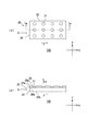
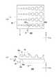
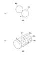
図1を参照して本発明による導光板100の実施形態を説明する。図1は、本発明の実施形態に係る導光板100を示す模式図である。図1(a)は導光板100の上面図である。図1(b)は図1(a)の1a−1a’線に沿った断面図である。[Embodiment 1 of Light Guide Plate]
An embodiment of a
導光板100は、導光部材20と、拡散部材30とを備える。導光部材20と拡散部材30とは各々2つの主面を有する。導光部材20は、主面24aと主面24bとを有する。拡散部材30は、主面30aと主面30bとを有する。拡散部材30は、導光部材20に隣接する主面30bとは反対側の拡散部材30の主面30aに複数の凹部31を有している。導光部材20の主面24a、主面24bはいずれもほぼ平坦であり、導光部材20の厚さはほぼ一定である。典型的には、導光部材20の主面24a、主面24bの面積は互いに等しい。
The
導光部材20は、例えば、PPMA(ポリメタクリル酸メチル樹脂)などのアクリル樹脂から形成される。光源(図示せず)は典型的に導光部材の周囲に設けられる。導光部材20の光入射面22は光源と対向しており、光源からの光は図1の矢印Liに示すように導光部材20の光入射面22から導光部材20内部に入射し、主面24aと主面24bとに沿った方向(x方向)の伝搬方向Pに伝搬する。光は導光部材20を伝搬方向Pに伝搬する過程で主面24aと主面24bとに対して鉛直方向(z方向:図1の矢印Lo)に導光部材20の主面24a側から出射される。なお、本明細書の以下の説明において、主面24a、主面24bをそれぞれ第1主面24a、第2主面24bと記載することがある。
The
拡散部材30は、導光部材20の第1主面24aおよび第2主面24bの少なくとも一方に設けられている。図1に示した導光板100では、拡散部材30は、導光部材20の主面24aに設けられている。拡散部材30は導光部材20と同じ材料から形成されてもよく、異なる材料から形成されても良い。異なる材料から形成された場合は、導光部材20の主面24aと拡散部材30との界面において屈折率は変化する。
The
拡散部材30は、例えば、アクリル系の樹脂、ポリイミド系の樹脂から形成される。あるいは、拡散部材30はビーズを含有してもよい。例えば、ビーズはアモルファスシリカまたはアクリルから形成され、その平均粒径は約1μm程度である。
The
拡散部材30の凹部31の凹面に入射した光は、拡散部材30の凹部31の凹面において拡散する。拡散部材30の凹部31の凹面に入射する光は、導光部材20内を反射して凹面に到達した光に加え、拡散部材30内に入射して凹面に到達した光でもあり得る。
The light incident on the concave surface of the
凹部31は伝搬方向Pに沿って配列されている。具体的には、導光部材20の主面24aを法線方向から見た場合、凹部31の中心はほぼ伝搬方向Pに沿って直線状に配列されている。
The
例えば、凹部31のx方向に沿った長さ(幅)とy方向に沿った長さ(幅)は20μm〜70μmである。また、凹部31の厚さ(z方向の長さ)は、例えば、5μmである。詳細は後述するが、このような微細な凹部31はグラビアオフセット印刷で好適に形成できる。このように微細な凹部31を設けることにより、光を適切に拡散させることができる。典型的に液晶表示装置に導光板を用いる場合、光を拡散させるために拡散板が設けられるが、凹部31を設けることにより、光を適切に拡散させることができるため液晶表示装置から拡散板を省略することができる。
For example, the length (width) along the x direction and the length (width) along the y direction of the
図1を参照して説明したように、導光板100は、拡散部材30の複数の凹部31から光を拡散する。従って、光を拡散する部分が突出していないため、光を拡散する部分が損傷することが無い。その結果、光の均一性が損なわれるおそれを無くすことができる。
As described with reference to FIG. 1, the
[導光板の実施形態2]
図2は、本発明の他の実施形態に係る導光板200を示す模式図である。導光板200は、導光部材20と、拡散部材40とを備える。拡散部材40は、第1層40aと第2層40bと第3層40cとを含む複数の層から形成されている。導光板200は、拡散部材40が複数の層から形成される点を除いて図1を参照して説明した導光板100と同様な構成を有するため、重複部分については説明を省略する。[Embodiment 2 of the light guide plate]
FIG. 2 is a schematic view showing a
第2層40bは第1層40aの上部、第3層40cは第2層40bの上部に積層されている。第1層40aと第2層40bと第3層40cとのそれぞれは複数の開口部を有し、第1層40aの有する複数の開口部と第2層40bの有する複数の開口部と第3層40cの有する複数の開口部とが互いに整合することで複数の凹部41が形成される。
The
第1層と第2層と第3層とを形成する材料は、同じであってもよいし、いずれかが異なってもよい。例えば、第1層40aの材料には導光部材20と同じ材料であるPPMA(ポリメタクリル酸メチル樹脂)などのアクリル樹脂を用いる。第2層40bの材料にはガラスフリット、バブルなどを混入したアクリル系インクを用いる。第3層40cの材料には導光部材20と反射率、屈折角が異なる材料を用いる。拡散部材40の材料にガラスフリット、バブルなどを混入したアクリル系インクを用いることにより、入射した光が乱反射しやすくなり、光を拡散させることができる。拡散部材40の材料に反射率、屈折角が異なる材料を用いることにより、反射効率が高くなる。
The materials forming the first layer, the second layer, and the third layer may be the same, or any of them may be different. For example, an acrylic resin such as PPMA (polymethyl methacrylate resin) which is the same material as the
図2を参照して説明したように、導光板200の拡散部材40は複数の層から形成されている。従って、異なる材料から拡散部材を形成することができる。その結果、拡散部材の材料の組み合わせの選択の自由度が向上する。
As described with reference to FIG. 2, the
[導光板の実施形態3]
図3は、本発明の更に他の実施形態に係る導光板300aおよび300bを示す模式図である。図3(a)は拡散部材40の凹部の凹面が凹凸形状でない導光板300aを示し、図3(b)は拡散部材40の凹部の凹面が凹凸形状である導光板300bを示す。導光板300aは、図2を参照して説明した導光板200と同様な構成を有するため、重複部分については説明を省略する。導光板300bは、拡散部材40の凹部の凹面が凹凸形状である点を除いて図2を参照して説明した導光板200と同様な構成を有するため、重複部分については説明を省略する。[Embodiment 3 of the light guide plate]
FIG. 3 is a schematic diagram showing
導光板300bは、導光部材20と、拡散部材40とを備える。拡散部材40の凹部41の凹面が凹凸形状である。第2層40bは第1層40a及び第3層40cに対してずれて積層されている。拡散部材40の凹部41の凹面が凹凸形状であることにより、光を乱反射させることができる。凹凸形状の凹凸幅が大きいほど、より光を乱反射させることができるため、凹凸形状の凹凸幅は大きい方が好ましい。ただし光の出口が閉じてはならない。例えば、凹部の開口部の径が20μmの場合は、凹凸形状の凹凸幅は0μm〜10μmである。例えば、凹部の開口部の径が70μmの場合は、凹凸形状の凹凸幅は0μm〜35μmである。
The
なお、拡散部材40を形成するインクを印刷する以前に、導光部材20の主面24a全体に凹凸形状が形成されるようにしてもよい。導光部材20の主面24a全体に凹凸形状を形成することにより、凹部41の凹面の底面に凹凸が形成される。底面の凹凸の厚さは、例えば、0.5nm〜10μmである。例えば、グラビアオフセット印刷で底面の凹凸を形成する場合、厚さは2μmである。凹面の底面に凹凸を形成することにより、凹部41の底面でも光を乱反射させることができる。その結果光を拡散することができる。
In addition, before printing the ink which forms the diffusing
図3(b)を参照して説明したように、導光板300bの拡散部材40の凹部41の凹面が凹凸形状である。従って、光を乱反射させることができる。その結果、光を拡散させることができ、導光板の拡散効率を向上させることができる。
As described with reference to FIG. 3B, the concave surface of the
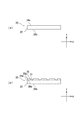
[導光板の実施形態4]
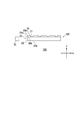
図4は、本発明の更に他の実施形態に係る導光板400を示す模式図である。図4(a)は導光板400の上面図であり、図4(b)は導光板400の50a−50a’線に沿った断面図である。[Embodiment 4 of Light Guide Plate]
FIG. 4 is a schematic view showing a
導光板400は、導光部材20と、拡散部材30とを備える。拡散部材30が有する2つの主面のうち、導光部材20に隣接する主面30bとは反対側の拡散部材30の主面30aに複数の凹部31を有している。導光板400は、凹部31の大きさが光入射面22からの距離に応じて異なる点を除いて図1を参照して説明した導光板100と同様な構成を有するため、重複部分については説明を省略する。
The
導光板400では、凹部31の大きさは光入射面22からの距離に応じて異なる。凹部31は、光入射面22から離れるほど主面24aを法線方向から見た場合の大きさが大きくなるように配列されている。典型的には、光入射面から入射した光は、伝搬距離が長くなるほど導光板内での反射により減衰するため、導光板から拡散される光の強度は光入射面から離れるほど減少する。しかしながら、本実施形態の導光板400では、凹部31は、光入射面22から離れるほど大きさが増加するように配列されており、光入射面22から離れる程反射効率があがる。光入射面22から離れるほど凹部31に到達する光の量が少なくなるが、導光板400からの光の強度を均一化することができる。
In the
ここで、同一直線上(x方向に沿った直線上)に配列された互いに隣接する2つの凹部(凹部31a、凹部31b)に着目する。導光部材20の主面24aを法線方向から見た場合、凹部31bと光入射面22との間の距離は、凹部31aと光入射面22との間の距離よりも大きい。ここでは、凹部31a、凹部31bのそれぞれは円形状を有している。なお、本明細書の以下の説明において、凹部31a、凹部31bをそれぞれ第1凹部31a、第2凹部31bと記載することがある。
Here, attention is focused on two adjacent concave portions (the
図4を参照して説明したように、凹部31aおよび凹部31bの中心が光入射面22から入射された光の伝搬方向Pに沿うように凹部31aおよび凹部31bは配列されている。導光部材20の主面24aを法線方向から見た場合、第2凹部31bの大きさは第1凹部31aの大きさよりも大きい。このため、本実施形態の導光板400では、主面24a全体だけでなく、各凹部31の近傍を局所的に見た場合でも、光入射面22から離れるほど大きさが増加するように構成されており、導光板400からの光の強度をさらに均一化することができる。本実施形態の導光板400では、凹部31を光入射面22から離れるほど大きさが増加するように設けることにより、拡散効率を向上させている。
As described with reference to FIG. 4, the
図5は、本発明の更に他の実施形態に係る導光板500を示す模式図である。図5(a)は導光板500の上面図であり、図5(b)は導光板500の50b−50b’線に沿った断面図である。
FIG. 5 is a schematic view showing a
導光板500は、導光部材20と、拡散部材30とを備える。拡散部材30が有する2つの主面である主面30aと主面30bとのうち、導光部材20に隣接する主面30bとは反対側の拡散部材30の主面30aに複数の凹部31を有している。導光板500は、凹部31のくぼみ(z方向の長さ)が光入射面22からの距離応じて異なる点を除いて図4を参照して説明した導光板400と同様な構成を有するため、重複部分については説明を省略する。
The
本実施形態の導光板500では、凹部31のくぼみ(z方向の長さ)は光入射面22からの距離に応じて異なる。凹部31は、光入射面22から離れるほどくぼみ(z方向の長さ)が大きくなるように配列されている。例えば、光入射面22から近い凹部31から順番に、1μm、2μm、3μm、4μmである。
In the
[導光板の実施形態5]
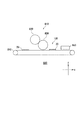
図6は、本発明の他の実施形態に係る導光板600の模式図である。導光板600は、導光部材20と、拡散部材30と、反射フィルム60とを備える。導光板600は、反射フィルム60を備える点を除いて図1を参照して説明した導光板100と同様な構成を有するため、重複部分については説明を省略する。[Embodiment 5 of Light Guide Plate]
FIG. 6 is a schematic view of a
導光板600は、導光部材20が有する2つの主面である主面24aと主面24bとのうち、拡散部材30に隣接する主面24aとは反対側の導光部材20の主面24bに反射フィルム60を備える。すなわち導光板600において、光の出射方向Loと反対側の主面24bに反射フィルムは備えられる。反射フィルム60は主面24bに到達した光を反射する。反射フィルムは、例えば、芳香族ポリエステル系樹脂に酸化チタンを添加して形成された白色シートである。反射フィルム60の厚さは、例えば、15μm〜25μmであるが、200μm程度でもありえる。反射フィルム60を設けることにより、主面24bから漏れる光を反射させることができる。その結果、光の使用効率があがる。
The
従来の導光板では光はドットパターンが形成されている主面と反対側の主面から出射するため、反射フィルムをドットパターンが形成されている主面側に形成しなければならなかった。しかしながら、ドットパターンが突出しているため、ドットパターンと反射フィルムとの間に空気層を設ける必要があった。一方、導光板600においては、光の出射方向Loは拡散部材が形成されている主面24aと同じ主面側になるため、反射フィルムを主面24bに形成すればよい。従って、反射フィルム60を平らな面に設けることができるので、空気層を設ける必要が無い。また、拡散部材と反対側の主面に反射フィルム60を設けるので、反射フィルム60が拡散部材30と接触することによる拡散部材の損傷のおそれがない。また空気層が無いので、空気層による光の損失が無く、発光効率を向上することができる。反射フィルム60は平らな面に設けられ、印刷により反射フィルム60を設けることができる。
In the conventional light guide plate, since light is emitted from the main surface opposite to the main surface on which the dot pattern is formed, the reflection film has to be formed on the main surface side on which the dot pattern is formed. However, since the dot pattern protrudes, it is necessary to provide an air layer between the dot pattern and the reflective film. On the other hand, in the
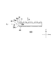
[光源装置の実施形態1]
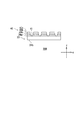
図7は、本発明の実施形態に係る光源装置700を示す模式図である。光源装置700は、導光板100と光源70とを備える。導光板100は、図1を参照して説明した導光板100と同様な構成を有するため、重複部分については説明を省略する。光源70は導光板100の光入射面22に対向するように設けられる。光源70は導光部材20に対して入射する光を発する。照明器具として、光源装置700を使用することができる。[Embodiment 1 of Light Source Device]
FIG. 7 is a schematic diagram showing a
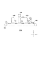
[導光板製造装置の実施形態1]
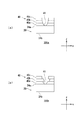
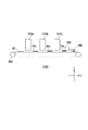
以下、図8および図9を参照して本発明による導光板製造装置800の実施形態を説明する。図8は、本発明の実施形態に係る導光板製造装置800を示す模式図である。図9(a)は、印刷部810を示す模式図である。図9(b)は、版ロール820を示す模式図である。導光板製造装置800は、図1を参照して説明した導光板100を製造する。以下の説明において、導光板製造装置800を単に製造装置800と記載することがある。[Embodiment 1 of light guide plate manufacturing apparatus]
Hereinafter, an embodiment of a light guide
製造装置800は、印刷部810を備える。印刷部810は、版ロール820および転写ロール830を備える。印刷部810は、拡散部材30を形成するインクを導光部材20に印刷する。版ロール820および転写ロール830はそれぞれ回転可能である。ここでは、版ロール820および転写ロール830の直径はほぼ等しい。
The
版ロール820の表面は金属メッキで処理されている。典型的には、版ロール820には、所定のパターンで凹溝が形成されている。このパターンは、導光部材20に印刷される線・図形・模様その他に対応する。転写ロール830は金属管とブランケットを含み、ブランケットは金属管の外周面を覆うように設けられている。典型的には、ブランケットはゴムから形成される。例えば、ブランケットは、シリコーンのゴムから形成される。金属管は、例えば、鉄、アルミから形成される。
The surface of the
版ロール820の表面にはインク充填部821と、拡散部材30が有する複数の凹部31に対応する形状である複数の凸部822が設けられている(図9(b))。ここで、互いに隣接する2つの凸部822a、凸部822bに着目する。本明細書の以下の説明において、凸部822a、凸部822bをそれぞれ第1凸部822a、第2凸部822bと記載することがある。版ロール820の回転方向に沿った方向を方向Rとした場合、第1凸部822aおよび第2凸部822bは方向Rに沿って設けられる。
The surface of the
なお、図9(b)では、直線状に配列された凸部822a、凸部822bの方向Rは、版ロール820の回転方向に沿って設けられたが、本発明はこれに限定されない。方向Rは円柱状の版ロール820の母線の方向に沿っていてもよい。
In FIG. 9B, the direction R of the
製造装置800において、導光部材20は版ロール820および転写ロール830の位置まで搬送されることが好ましい。例えば、図8に示すように、製造装置800は、導光部材20を搬送する搬送部840をさらに備える。ここでは、搬送部840はコンベアであり、搬送部840は、固定された版ロール820および転写ロール830に対して導光部材20を搬送する。製造装置800は、インクを乾燥させる乾燥装置850をさらに備えてもよい。
In the
[導光板製造方法の実施形態1]
図10は、本発明の導光板の製造方法を説明するための模式図である。以下、図8〜図10を参照して、導光板100の製造方法の一例を説明する。はじめに、図10(a)に示すように、光入射面22、主面24a、主面24bを有する導光部材20を用意する。[Embodiment 1 of light guide plate manufacturing method]
FIG. 10 is a schematic view for explaining the method of manufacturing the light guide plate of the present invention. Hereinafter, an example of a method for manufacturing the
図10(b)に示すように、導光部材20の主面24aに拡散部材30を形成するインクを印刷する。拡散部材30は導光部材20に隣接する主面30bとは反対側の拡散部材30の主面30aに複数の凹部31を有している。なお、ここでは、拡散部材30を形成するインクは導光部材20の主面24aに印刷されたが、拡散部材30を形成するインクは導光部材20の主面24bに印刷されてもよく、あるいは、主面24a、主面24bの両方に印刷されてもよい。
As shown in FIG. 10B, the ink that forms the
典型的には、導光部材20はPPMA(ポリメタクリル酸メチル樹脂)などのアクリル樹脂から形成される。また、典型的には、製造装置800では、版ロール820は金属から形成され、転写ロール830のブランケットは樹脂から形成される。このように、製造装置800では、版ロール820ではなく転写ロール830のブランケットが導光部材20と直接接触するため、アクリル樹脂への物理的衝撃を抑制することができる。
Typically, the
このように導光板100をグラビアオフセット印刷で製造することが好ましい。グラビアオフセット印刷により、拡散部材30の材料使用量を低減するとともに、拡散部材30を簡便かつ高速に形成できる。また、グラビアオフセット印刷により、微細な複数の凹部31を実現することができ、また、導光部材20とは異なる材料で拡散部材30を形成することができる。なおグラビアオフセット印刷を行う場合でも、拡散部材30を導光部材20とほぼ同じ材料から形成してもよい。
Thus, it is preferable to manufacture the
[導光板製造装置の実施形態2]
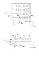
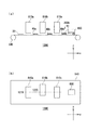
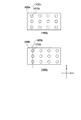
図11は、本発明の他の実施形態に係る導光板製造装置1100を示す模式図である。導光板製造装置1100は、図2を参照して説明した導光板200を製造する。導光板製造装置1100は第1印刷部810aと第2印刷部810bと第3印刷部810cとを備える。導光板製造装置1100は、印刷部を複数備える点を除いて図8を参照して説明した導光板製造装置800と同様な構成を有するため、重複部分については説明を省略する。以下の説明において、導光板製造装置1100を単に製造装置1100と記載することがある。[Embodiment 2 of light guide plate manufacturing apparatus]
FIG. 11 is a schematic view showing a light guide
製造装置1100は、複数の印刷部を備える。第1印刷部810aは第1転写ロールと拡散部材40の第1層40aの形状に対応する第1版ロールとを有する。第2印刷部810bは第2転写ロールと拡散部材40の第2層40bの形状に対応する第2版ロールとを有する。第3印刷部810cは第3転写ロールと拡散部材40の第3層40cの形状に対応する第3版ロールとを有する。第1版ロールと第2版ロールと第3版ロールとの各々には、インク充填部と拡散部材が有する複数の凹部に対応する形状である複数の凸部とが形成されている。
The
[導光板製造方法の実施形態2]
以下、図11を参照して、導光板200の製造方法の一例を説明する。導光板200の製造方法は、第1工程と第2工程と第3工程とを包含する。最初に、搬送部840の上に導光部材20が載置され、搬送部840は導光部材20を搬送する。続いて、搬送部840によって搬送された導光部材20が第1印刷部810aの下に到達すると、第1印刷部810aは拡散部材40の第1層40aを形成するインクを導光部材20の上に積層するように印刷する(第1工程)。続いて、第1印刷部810aが印刷を行った後に、導光部材20が第2印刷部810bの下に到達すると、第2印刷部810bは拡散部材40の第2層40bを形成するインクを第1層40aの上に積層するように印刷する(第2工程)。続いて、第2印刷部810bが印刷を行った後に、導光部材20が第3印刷部810cの下に到達すると、第3印刷部810cは拡散部材40の第3層40cを形成するインクを第2層40bの上に積層するように印刷する(第3工程)。上述した第1工程、第2工程、第3工程を経て、導光部材20から導光板200を製造することができる。[Embodiment 2 of light guide plate manufacturing method]
Hereinafter, an example of a method for manufacturing the
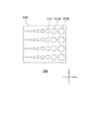
[導光板製造装置の実施形態3]
図12(a)は、本発明の更に他の実施形態に係る導光板製造装置1200を示す模式図であり、図12(b)は、本発明の他の実施形態に係る導光板製造装置1200の模式的な上面図である。導光板製造装置1200は、図3(b)を参照して説明した導光板300bを製造する。導光板製造装置1200は、拡散部材40の第2層40bが第1層40aに対してずれて印刷されるように第2印刷部810bを設けた点を除いて、図11を参照して説明した導光板製造装置1100と同様な構成を有するため、重複部分については説明を省略する。以下の説明において、導光板製造装置1200を単に製造装置1200と記載することがある。[Embodiment 3 of the light guide plate manufacturing apparatus]
FIG. 12A is a schematic diagram showing a light guide
製造装置1200は、複数の印刷部を備える。導光板製造装置1200は第1印刷部810aと第2印刷部810bと第3印刷部810cとを備える。図12(b)において、中心線1210は第1印刷部810aと第3印刷部810cとの中心を通る中心線を示す。中心線1220は第2印刷部810bの中心を通る中心線を示す。第2印刷部810bは、中心線1210に対して、y方向にずれて設けられる。中心線1210に対して、第2印刷部810bをy方向にずらして設けることにより、拡散部材40の第2層40bは、第1層40aと第3層40cとに対してy方向にずれて印刷される。その結果、拡散部材の凹部41の凹面が凹凸形状である導光板300bを製造することができる。
The
[導光板製造装置の実施形態4]
図13は、本発明の更に他の実施形態に係る導光板製造装置1300を示す模式図である。導光板製造装置1300は、図3(b)を参照して説明した導光板300bを製造する。導光板製造装置1300は、タイミング調整手段1310を更に備える点を除いて図11を参照して説明した導光板製造装置1100と同様な構成を有するため、重複部分については説明を省略する。以下の説明において、導光板製造装置1300を単に製造装置1300と記載することがある。[Embodiment 4 of the light guide plate manufacturing apparatus]
FIG. 13 is a schematic diagram showing a light guide
製造装置1300はタイミング調整手段1310を更に備えている。タイミング調整手段1310は、拡散部材40の第2層40bが第1層40aに対してずれて印刷されるように第2層40bの印刷タイミングを調整する。例えば、第1印刷部810aの転写ロールと第2印刷部810bの転写ロールの回転速度が同じ場合は、拡散部材40の第2層40bが第1層40aに対してずれて印刷されるように、第1印刷部810aの転写ロールの印刷開始位置に対して第2印刷部810bの転写ロールの印刷開始位置をずらす。または、拡散部材40の第2層40bが第1層40aに対してずれて印刷されるように、第2印刷部810bの転写ロールの回転速度を調整する。例えば、第1層40aを印刷後に、導光部材20に印刷された拡散部材40の第1層40aの位置を測定し、測定された第1層40aの位置に基づいて、転写ロールの回転速度を調整する。
The
[導光板製造装置の実施形態5]
図14は、本発明の更に他の実施形態に係る導光板製造装置の版ロールの展開図である。図14の上図は第1版ロール1400aの展開図であり、図14の下図は第2版ロール1400bの展開図である。[Embodiment 5 of the light guide plate manufacturing apparatus]
FIG. 14 is a development view of a plate roll of a light guide plate manufacturing apparatus according to still another embodiment of the present invention. The upper view of FIG. 14 is a development view of the
第1版ロール1400aは、複数の凸部1410aとインク充填部1420aとを有する。第2版ロール1400bは、複数の凸部1410bとインク充填部1420bとを有する。中心線1430aは凸部1410aの中心線を示し、中心線1430bは凸部1410bの中心線を示す。中心線1430bは中心線1430aに対してx方向にずれている。第2版ロール1400bの複数の凸部1410bは第1版ロール1400aの複数の凸部1410aに対して所定方向にずれており、その結果、第1層40aと第2層40bとはずれて印刷されるので、図3(b)を参照して説明した導光板300bを製造することができる。第2版ロール1400bでは、第1版ロール1400aに対してx方向にずらしたが、第1版ロール1400aに対して第2版ロール1400bをy方向にずらしてもよい。
The
[導光板製造装置の実施形態6]
図15は、本発明の更に他の実施形態に係る導光板製造装置の版ロール1500の展開図である。[
FIG. 15 is a development view of a
版ロール1500は、第1凸部1510aおよび第2凸部1510bを含む複数の凸部1510とインク充填部1520とが設けられている。第1凸部1510aおよび第2凸部1510bはx方向に沿って設けられており、第2凸部1510bの大きさは第1凸部1510aの大きさよりも大きい。版ロール1500を使用することにより、図4を参照して説明した導光板400、及び図5を参照して説明した導光板500を製造することができる。
The
[導光板製造装置の実施形態7]
図16は、本発明の更に他の実施形態に係る導光板製造装置1600を示す模式図である。導光板製造装置1600は、図6を参照して説明した導光板600を製造する。導光板製造装置1600は、印刷部1610と反射フィルム印刷部1620とを備える。印刷部1610は版ロール1611と転写ロール1612とを備える。反射フィルム印刷部1620は版ロール1621と転写ロール1622とを備える。反射フィルム印刷部1620は、印刷部1610と対向する位置に設けられる。印刷部1610は、導光部材20の主面24aに、拡散部材30を形成するインクを印刷する。反射フィルム印刷部1620は、導光部材20の主面24bに、反射フィルム60を形成するインクを印刷する。導光板製造装置1600は、導光部材20を搬送する搬送部1630と搬送部1631とをさらに備えてもよい。搬送部1630と搬送部1631とはコンベアである。搬送部1630と搬送部1631とは、導光部材20を搬送する。搬送部1631は、反射フィルム印刷部1620を介して搬送部1630と対向する位置に設けられる。導光板製造装置1600は、拡散部材30を形成するインク及び反射フィルム60を形成するインクを乾燥させる乾燥装置850をさらに備えてもよい。インクがUVによって硬化する場合、乾燥装置850の代わりにUVランプを備えてもよい。[Embodiment 7 of Light Guide Plate Manufacturing Apparatus]
FIG. 16 is a schematic view showing a light guide
なお、導光板製造装置1600では、導光部材20の主面24aと主面24bとが鉛直方向(z方向)に向くように導光部材20を搬送したが、導光部材の主面24aと主面24bが水平方向(y方向)に向くように導光部材20を搬送し、導光部材20を印刷部1610と反射フィルム印刷部1620とで水平方向(y方向)から挟むことにより導光板600を製造してもよい。
In the light guide
本明細書において、拡散部材40が第1層40aと第2層40bとを含む複数の層から形成される導光板200の実施形態、第1層40aと第2層40bとの各々が、同じ材料から形成される導光板200の実施形態、第1層40aと第2層40bとの各々が、異なる材料から形成される導光板200の実施形態、複数の凹部41の凹面が凹凸形状である導光板300bの実施形態、第2凹部31bの大きさは第1凹部31aの大きさよりも大きい導光板400および導光板500の実施形態、さらに反射フィルム60を備える導光板600の実施形態を説明したが、これら導光板の実施形態のうちの少なくとも2つの実施形態の構成要素を当業者が明らかなように組み合わせた実施形態も本発明の実施形態である。
In this specification, the embodiment of the
本発明の導光板は、液晶表示装置または照明装置等に好適に用いられる。 The light guide plate of the present invention is suitably used for a liquid crystal display device or a lighting device.
20 導光部材
22 光入射面
24a、24b 導光部材の主面
30 拡散部材
30a、30b 拡散部材の主面
31 凹部
31a 第1凹部
31b 第2凹部
40 拡散部材
40a 第1層
40b 第2層
40c 第3層
41 凹部
60 反射フィルム
70 光源
100 導光板
200 導光板
300a 導光板
300b 導光板
400 導光板
500 導光板
600 導光板
700 導光板
800 導光板製造装置
810 印刷部
810a 第1印刷部
810b 第2印刷部
810c 第3印刷部
820 版ロール
821 インク充填部
822 凸部
822a 第1凸部
822b 第2凸部
830 転写ロール
840 搬送部
850 乾燥装置
1100 導光板製造装置
1200 導光板製造装置
1300 導光板製造装置
1310 タイミング調整手段
1400a 第1版ロール
1400b 第2版ロール
1410a、1410b 凸部
1420a、1420b インク充填部
1430a、1430b 中心線
1500 版ロール
1510 凸部
1510a 第1凸部
1510b 第2凸部
1520 インク充填部
1600 導光板製造装置
1610 印刷部
1611 版ロール
1612 転写ロール
1620 反射フィルム印刷部
1621 版ロール
1622 転写ロール
1630、1631 搬送部20
Claims (12)
前記導光部材の前記第1主面および前記第2主面のうちの少なくとも一方に隣接して設けられた拡散部材と
を備える導光板であって、
前記拡散部材が有する2つの主面のうち、前記導光部材に隣接する主面とは反対側の前記拡散部材の主面に複数の凹部を有し、前記導光部材に入射した光を前記複数の凹部で拡散させ、
前記複数の凹部の凹面は凹凸形状であり、
前記拡散部材は、第1開口部の設けられた第1層と、第2開口部の設けられた第2層とを含む複数の層から形成され、
前記第2層の前記第2開口部は前記第1層の前記第1開口部と連通し、前記第2層の前記第2開口部が前記第1層の前記第1開口部に対してずれるように前記第2層は前記第1層上に配置される、導光板。 A light guide member having a first main surface and a second main surface;
A light guide plate comprising a diffusion member provided adjacent to at least one of the first main surface and the second main surface of the light guide member,
Of the two main surfaces of the diffusion member, the main surface of the diffusion member opposite to the main surface adjacent to the light guide member has a plurality of recesses, and the light incident on the light guide member is Diffuse in multiple recesses,
The concave surfaces of the plurality of concave portions are concave and convex shapes,
The diffusion member is formed of a plurality of layers including a first layer provided with a first opening and a second layer provided with a second opening,
The second opening of the second layer communicates with the first opening of the first layer, without the second opening of the second layer have to the first opening of the first layer The light guide plate, wherein the second layer is disposed on the first layer.
前記導光部材の前記第1主面を法線方向から見た場合、
光の入射面と前記第2凹部との間の距離は前記光の入射面と前記第1凹部との間の距離よりも大きく、前記第2凹部の大きさは前記第1凹部の大きさよりも大きい、請求項1に記載の導光板。 The plurality of recesses include a first recess and a second recess,
When the first main surface of the light guide member is viewed from the normal direction,
The distance between the light incident surface and the second concave portion is larger than the distance between the light incident surface and the first concave portion, and the size of the second concave portion is larger than the size of the first concave portion. The light guide plate according to claim 1, which is large.
前記導光部材に対して入射する光を発する光源と
を備える、光源装置。 The light guide plate according to claim 1, and
And a light source that emits light incident on the light guide member.
前記印刷部は、版ロールと転写ロールとを備え、
前記版ロールには、インク充填部と、前記拡散部材が有する複数の凹部に対応する形状である複数の凸部とが形成されており、
前記版ロールは、前記インク充填部に充填された前記インクを前記転写ロールに転写し、
前記転写ロールは、前記インクを前記導光部材に印刷し、
前記拡散部材は、第1層と第2層とを含む複数の層を有し、
前記導光板製造装置は、
前記拡散部材の前記第1層を形成するインクを印刷する第1印刷部と
前記拡散部材の前記第2層を形成するインクを印刷する第2印刷部と
を備え、
前記第1印刷部は、第1転写ロールと前記第1層の形状に対応する第1版ロールとを有し、
前記第2印刷部は、第2転写ロールと前記第2層の形状に対応する第2版ロールとを有し、
前記第2層が前記第1層に対してずれて印刷されるように前記第2印刷部を設ける、導光板製造装置。 A light guide plate manufacturing apparatus including a printing unit that prints ink forming a diffusion member on a light guide member,
The printing unit includes a plate roll and a transfer roll,
The plate roll is formed with an ink filling portion and a plurality of convex portions having a shape corresponding to the plurality of concave portions of the diffusion member,
The plate roll transfers the ink filled in the ink filling portion to the transfer roll,
The transfer roll prints the ink on the light guide member,
The diffusion member has a plurality of layers including a first layer and a second layer,
The light guide plate manufacturing apparatus includes:
A first printing unit that prints ink that forms the first layer of the diffusion member; and a second printing unit that prints ink that forms the second layer of the diffusion member;
The first printing unit includes a first transfer roll and a first plate roll corresponding to the shape of the first layer,
The second printing unit includes a second transfer roll and a second plate roll corresponding to the shape of the second layer,
An apparatus for manufacturing a light guide plate, wherein the second printing unit is provided so that the second layer is printed out of alignment with the first layer.
前記印刷部は、版ロールと転写ロールとを備え、
前記版ロールには、インク充填部と、前記拡散部材が有する複数の凹部に対応する形状である複数の凸部とが形成されており、
前記版ロールは、前記インク充填部に充填された前記インクを前記転写ロールに転写し、
前記転写ロールは、前記インクを前記導光部材に印刷し、
前記拡散部材は、第1層と第2層とを含む複数の層を有し、
前記導光板製造装置は、
前記拡散部材の前記第1層を形成するインクを印刷する第1印刷部と
前記拡散部材の前記第2層を形成するインクを印刷する第2印刷部と
を備え、
前記第1印刷部は、第1転写ロールと前記第1層の形状に対応する第1版ロールとを有し、
前記第2印刷部は、第2転写ロールと前記第2層の形状に対応する第2版ロールとを有し、
前記第2層が前記第1層に対してずれて印刷されるように前記第2層の印刷タイミングを調整するタイミング調整手段を設ける、導光板製造装置。 A light guide plate manufacturing apparatus including a printing unit that prints ink forming a diffusion member on a light guide member,
The printing unit includes a plate roll and a transfer roll,
The plate roll is formed with an ink filling portion and a plurality of convex portions having a shape corresponding to the plurality of concave portions of the diffusion member,
The plate roll transfers the ink filled in the ink filling portion to the transfer roll,
The transfer roll prints the ink on the light guide member,
The diffusion member has a plurality of layers including a first layer and a second layer,
The light guide plate manufacturing apparatus includes:
A first printing unit that prints ink that forms the first layer of the diffusion member; and a second printing unit that prints ink that forms the second layer of the diffusion member;
The first printing unit includes a first transfer roll and a first plate roll corresponding to the shape of the first layer,
The second printing unit includes a second transfer roll and a second plate roll corresponding to the shape of the second layer,
An apparatus for manufacturing a light guide plate, comprising: a timing adjusting unit that adjusts a printing timing of the second layer so that the second layer is printed out of alignment with the first layer.
前記印刷部は、版ロールと転写ロールとを備え、
前記版ロールには、インク充填部と、前記拡散部材が有する複数の凹部に対応する形状である複数の凸部とが形成されており、
前記版ロールは、前記インク充填部に充填された前記インクを前記転写ロールに転写し、
前記転写ロールは、前記インクを前記導光部材に印刷し、
前記拡散部材は、第1層と第2層とを含む複数の層を有し、
前記導光板製造装置は、
前記拡散部材の前記第1層を形成するインクを印刷する第1印刷部と
前記拡散部材の前記第2層を形成するインクを印刷する第2印刷部と
を備え、
前記第1印刷部は、第1転写ロールと前記第1層の形状に対応する第1版ロールとを有し、
前記第2印刷部は、第2転写ロールと前記第2層の形状に対応する第2版ロールとを有し、
前記第1版ロールと前記第2版ロールとにはそれぞれ前記拡散部材が有する複数の凹部に対応する形状である複数の凸部が形成されており、前記第2版ロールの前記複数の凸部は前記第1版ロールの前記複数の凸部に対して所定方向にずれている、導光板製造装置。 A light guide plate manufacturing apparatus including a printing unit that prints ink forming a diffusion member on a light guide member,
The printing unit includes a plate roll and a transfer roll,
The plate roll is formed with an ink filling portion and a plurality of convex portions having a shape corresponding to the plurality of concave portions of the diffusion member,
The plate roll transfers the ink filled in the ink filling portion to the transfer roll,
The transfer roll prints the ink on the light guide member,
The diffusion member has a plurality of layers including a first layer and a second layer,
The light guide plate manufacturing apparatus includes:
A first printing unit that prints ink that forms the first layer of the diffusion member; and a second printing unit that prints ink that forms the second layer of the diffusion member;
The first printing unit includes a first transfer roll and a first plate roll corresponding to the shape of the first layer,
The second printing unit includes a second transfer roll and a second plate roll corresponding to the shape of the second layer,
The first plate roll and the second plate roll are formed with a plurality of convex portions each having a shape corresponding to the plurality of concave portions of the diffusion member, and the plurality of convex portions of the second plate roll. Is a light guide plate manufacturing apparatus that is displaced in a predetermined direction with respect to the plurality of convex portions of the first plate roll.
前記第1凸部および前記第2凸部は所定の方向に沿って設けられており、
前記第2凸部の大きさは前記第1凸部の大きさよりも大きい、請求項7から請求項9のうちの1項に記載の導光板製造装置。 The plate roll is provided with a plurality of convex portions including a first convex portion and a second convex portion,
The first convex portion and the second convex portion are provided along a predetermined direction,
The light guide plate manufacturing apparatus according to claim 7, wherein a size of the second convex portion is larger than a size of the first convex portion.
前記反射フィルム印刷部は、前記印刷部と対向して設けられる、請求項7から請求項10のうちの1項に記載の導光板製造装置。 A reflection film printing unit for printing ink forming the reflection film;
The light guide plate manufacturing apparatus according to claim 7, wherein the reflection film printing unit is provided to face the printing unit.
インク充填部および複数の凸部が形成されている版ロールと転写ロールとを用いて、前記導光部材の前記第1主面および前記第2主面のうちの少なくとも一方に隣接するようにインクを印刷して、前記複数の凸部に対応する複数の凹部を有する拡散部材を形成する印刷工程と
を包含する導光板製造方法であって、
前記拡散部材が有する2つの主面のうち、前記導光部材に隣接する主面とは反対側の前記拡散部材の主面に前記複数の凹部を有し、前記導光部材に入射した光を前記複数の凹部で拡散させ、
前記拡散部材は、第1開口部の設けられた第1層と、第2開口部の設けられた第2層とを含む複数の層を有し、
前記印刷工程は、
前記拡散部材の前記第1層を形成するインクを印刷する第1工程と、
前記拡散部材の前記第2層を形成するインクを印刷する第2工程と
を包含し、
前記第2工程において、前記第2層の前記第2開口部は前記第1層の前記第1開口部と連通し、前記第2層の前記第2開口部が前記第1層の前記第1開口部に対してずれるように前記第2層は前記第1層上に配置される、導光板製造方法。 A preparation step of preparing a light guide member having a first main surface and a second main surface;
Ink so as to be adjacent to at least one of the first main surface and the second main surface of the light guide member using a plate roll and a transfer roll on which an ink filling portion and a plurality of convex portions are formed. A light guide plate manufacturing method including a printing step of forming a diffusion member having a plurality of concave portions corresponding to the plurality of convex portions,
Of the two main surfaces of the diffusing member, the main surface of the diffusing member opposite to the main surface adjacent to the light guide member has the plurality of recesses, and the light incident on the light guide member Diffusing in the plurality of recesses,
The diffusion member has a plurality of layers including a first layer provided with a first opening and a second layer provided with a second opening,
The printing process includes
A first step of printing ink forming the first layer of the diffusion member;
A second step of printing ink forming the second layer of the diffusing member,
In the second step, the second opening of the second layer communicates with the first opening of the first layer, and the second opening of the second layer is the first of the first layer. wherein as not have to opening the second layer is disposed on the first layer, the light guide plate manufacturing method.
Applications Claiming Priority (3)
| Application Number | Priority Date | Filing Date | Title |
|---|---|---|---|
| JP2012166720 | 2012-07-27 | ||
| JP2012166720 | 2012-07-27 | ||
| PCT/JP2013/069653 WO2014017400A1 (en) | 2012-07-27 | 2013-07-19 | Light guide plate, light source device, light guide plate manufacturing device, and method for manufacturing light guide plate |
Publications (2)
| Publication Number | Publication Date |
|---|---|
| JPWO2014017400A1 JPWO2014017400A1 (en) | 2016-07-11 |
| JP6324311B2 true JP6324311B2 (en) | 2018-05-16 |
Family
ID=49997213
Family Applications (1)
| Application Number | Title | Priority Date | Filing Date |
|---|---|---|---|
| JP2014526896A Expired - Fee Related JP6324311B2 (en) | 2012-07-27 | 2013-07-19 | Light guide plate, light source device, light guide plate manufacturing apparatus, and light guide plate manufacturing method |
Country Status (7)
| Country | Link |
|---|---|
| US (1) | US9880340B2 (en) |
| EP (1) | EP2878877A4 (en) |
| JP (1) | JP6324311B2 (en) |
| KR (1) | KR101794792B1 (en) |
| CN (1) | CN104508357B (en) |
| TW (1) | TWI526722B (en) |
| WO (1) | WO2014017400A1 (en) |
Families Citing this family (6)
| Publication number | Priority date | Publication date | Assignee | Title |
|---|---|---|---|---|
| KR102825767B1 (en) * | 2019-01-24 | 2025-06-27 | 엘지이노텍 주식회사 | Lighting apparatus |
| JP6791284B2 (en) * | 2019-02-22 | 2020-11-25 | ダイキン工業株式会社 | Drain pan, drain pan unit, and air conditioner |
| KR102683664B1 (en) * | 2019-07-30 | 2024-07-11 | 주식회사 엘지화학 | Multi-functional sheet capable of diffusion and retroreflection, preparation method thereof and back light unit comprising the same |
| KR20210143501A (en) | 2020-05-20 | 2021-11-29 | 엘지이노텍 주식회사 | Ligith emitting moudle, lighting device having thereof, and taillamp |
| CN113156567B (en) | 2021-02-07 | 2022-09-02 | 捷开通讯(深圳)有限公司 | Light guide plate and display device |
| EP4647301A1 (en) * | 2024-05-09 | 2025-11-12 | FERRARI S.p.A. | Automotive lighting unit |
Family Cites Families (31)
| Publication number | Priority date | Publication date | Assignee | Title |
|---|---|---|---|---|
| JP2869826B2 (en) * | 1991-08-28 | 1999-03-10 | キヤノン株式会社 | Semiconductor manufacturing method |
| JPH0555103U (en) | 1991-12-27 | 1993-07-23 | オーツタイヤ株式会社 | Light guide plate device |
| JPH08160423A (en) * | 1994-12-02 | 1996-06-21 | Nissha Printing Co Ltd | Surface light source device and manufacturing method thereof |
| JP3673928B2 (en) * | 1995-08-15 | 2005-07-20 | ミネベア株式会社 | Manufacturing method of substrate used in planar light source device |
| JP3008932B2 (en) | 1998-07-17 | 2000-02-14 | 日本電気株式会社 | Back lighting device |
| JP3271660B2 (en) * | 1999-01-19 | 2002-04-02 | 恵和株式会社 | Light path control diffusion sheet and backlight unit using the same |
| US20030214719A1 (en) * | 2002-05-16 | 2003-11-20 | Eastman Kodak Company | Light diffuser containing perimeter light director |
| JP4073250B2 (en) | 2002-05-21 | 2008-04-09 | シチズン電子株式会社 | Backlight unit |
| CN1942788A (en) * | 2004-02-26 | 2007-04-04 | 他喜龙株式会社 | Light-diffusing sheet and backlight unit using the light-diffusing sheet |
| JP2007242856A (en) | 2006-03-08 | 2007-09-20 | Rohm Co Ltd | Chip-type semiconductor light emitting device |
| CN2921887Y (en) * | 2006-04-03 | 2007-07-11 | 中强光电股份有限公司 | Backlight module |
| KR101375485B1 (en) * | 2007-01-12 | 2014-03-18 | 코니카 미놀타 어드밴스드 레이어즈 인코포레이티드 | Antireflection film, process for producing antireflection film, polarizing plate, and display device |
| TWI530713B (en) | 2007-02-21 | 2016-04-21 | 王子控股股份有限公司 | Peak-valley pattern formed sheet and method for producing the same |
| DE102008021721A1 (en) * | 2007-05-08 | 2008-11-27 | Citizen Electronics Co., Ltd., Fujiyoshida-shi | Optical component, backlight unit and display device |
| JP5045263B2 (en) * | 2007-06-20 | 2012-10-10 | ソニー株式会社 | Printing apparatus and printing method |
| US20100195313A1 (en) | 2007-08-02 | 2010-08-05 | Masanori Hiraishi | Light-diffusing film and apparatus provided with the same |
| CN101363934B (en) | 2007-08-10 | 2011-08-31 | 北京京东方光电科技有限公司 | Method and device for processing light conducting plate |
| CN101910879B (en) * | 2008-01-24 | 2013-10-09 | 木本股份有限公司 | Light-diffusing sheet and backlight device using same |
| KR100867919B1 (en) | 2008-02-29 | 2008-11-10 | 주식회사 엘엠에스 | Optical element, backlight unit and liquid crystal display including same |
| JP4528902B2 (en) | 2008-08-06 | 2010-08-25 | 株式会社オプトデザイン | LIGHT SOURCE DEVICE, LIGHTING DEVICE, AND DISPLAY DEVICE |
| KR100986997B1 (en) * | 2008-08-12 | 2010-10-11 | 주식회사 엘엠에스 | Optical element, backlight unit and liquid crystal display having same |
| JP2010103068A (en) * | 2008-10-27 | 2010-05-06 | Kuroda Denki Kk | Method of manufacturing light guide plate, light guide plate, and light source device |
| CN101738649B (en) * | 2008-11-11 | 2012-03-21 | 国硕科技工业股份有限公司 | Multi-layer coated composite optical film structure |
| WO2010060033A1 (en) * | 2008-11-24 | 2010-05-27 | 3M Innovative Properties Company | Web converting methods for forming light guides and the light guides formed therefrom |
| JP5323469B2 (en) * | 2008-12-24 | 2013-10-23 | 古河電気工業株式会社 | LIGHTING DEVICE AND LIGHT MANUFACTURING METHOD FOR LIGHTING DEVICE |
| JP2010225562A (en) | 2009-03-25 | 2010-10-07 | Sharp Corp | Light guide and backlight system |
| TWI410680B (en) * | 2009-10-28 | 2013-10-01 | Coretronic Corp | Light guide plate and backlight module |
| US8888347B2 (en) * | 2009-12-17 | 2014-11-18 | Kimoto Co., Ltd. | Light diffusing sheet and backlight using same |
| JP2012053273A (en) | 2010-09-01 | 2012-03-15 | Sumitomo Chemical Co Ltd | Light guide plate and edge-lit type surface light source device using the same |
| KR101685754B1 (en) | 2011-04-04 | 2016-12-12 | 준 사카모토 | Light guide plate, method for creating light guide plate, and device for creating light guide plate |
| TWI553358B (en) * | 2011-12-23 | 2016-10-11 | 鴻海精密工業股份有限公司 | Light guide plate and backlight module using the same |
-
2013
- 2013-07-19 JP JP2014526896A patent/JP6324311B2/en not_active Expired - Fee Related
- 2013-07-19 US US14/417,380 patent/US9880340B2/en not_active Expired - Fee Related
- 2013-07-19 CN CN201380039968.9A patent/CN104508357B/en not_active Expired - Fee Related
- 2013-07-19 KR KR1020157003709A patent/KR101794792B1/en not_active Expired - Fee Related
- 2013-07-19 WO PCT/JP2013/069653 patent/WO2014017400A1/en not_active Ceased
- 2013-07-19 EP EP13822738.4A patent/EP2878877A4/en not_active Withdrawn
- 2013-07-23 TW TW102126321A patent/TWI526722B/en not_active IP Right Cessation
Also Published As
| Publication number | Publication date |
|---|---|
| TWI526722B (en) | 2016-03-21 |
| WO2014017400A1 (en) | 2014-01-30 |
| EP2878877A4 (en) | 2016-03-30 |
| CN104508357B (en) | 2018-01-23 |
| JPWO2014017400A1 (en) | 2016-07-11 |
| TW201413305A (en) | 2014-04-01 |
| EP2878877A1 (en) | 2015-06-03 |
| US20150212252A1 (en) | 2015-07-30 |
| KR101794792B1 (en) | 2017-11-07 |
| CN104508357A (en) | 2015-04-08 |
| US9880340B2 (en) | 2018-01-30 |
| KR20150032739A (en) | 2015-03-27 |
Similar Documents
| Publication | Publication Date | Title |
|---|---|---|
| JP6324311B2 (en) | Light guide plate, light source device, light guide plate manufacturing apparatus, and light guide plate manufacturing method | |
| US11536896B2 (en) | Light distribution structure and element, related method and uses | |
| JPWO2019182092A1 (en) | Optical device | |
| US8692962B2 (en) | Diffusion sheet and method of manufacturing the same, backlight, and liquid crystal display device | |
| CA2795265A1 (en) | Internal cavity optics | |
| KR20130000252A (en) | Light guide plate for backlight unit and manufacturing method thereof | |
| US10732341B2 (en) | Optical body, method for manufacturing optical body, and light-emitting apparatus | |
| TW201838812A (en) | Microstructured and patterned light guide plates and devices comprising the same | |
| JP6046606B2 (en) | Light guide plate, light guide plate manufacturing method, and light guide plate manufacturing apparatus | |
| US20130286687A1 (en) | Light guide with a printed film | |
| KR20130099890A (en) | Light guide plate and backlight unit | |
| KR100938162B1 (en) | Prism sheet and optical film having the same | |
| JP4001799B2 (en) | Manufacturing method of reflector | |
| CN103250076B (en) | Optical element and manufacturing method thereof, backlight unit using same and manufacturing method thereof | |
| JP4270828B2 (en) | Transfer master for forming fine irregular surface, manufacturing method thereof, and master manufacturing apparatus | |
| KR101211726B1 (en) | Pattern Light Guiding Plate Integrated Reflector and Method of Manufacture The Same | |
| JP2012074308A (en) | Light source unit and liquid crystal display device | |
| KR20080037308A (en) | Prism sheet, backlight unit having the same, and a manufacturing method thereof | |
| TW201017282A (en) | Method and structure of light-emitting uniformity for backlight module | |
| JP2004219449A (en) | Method of manufacturing reflection body, reflection body and liquid crystal display device | |
| JP2011146381A (en) | Backlight unit and image display device including the same | |
| KR20100091376A (en) | Optics sheet and backlight unit having the same | |
| KR20120086870A (en) | Display device |
Legal Events
| Date | Code | Title | Description |
|---|---|---|---|
| A529 | Written submission of copy of amendment under article 34 pct |
Free format text: JAPANESE INTERMEDIATE CODE: A5211 Effective date: 20150126 |
|
| A621 | Written request for application examination |
Free format text: JAPANESE INTERMEDIATE CODE: A621 Effective date: 20160705 |
|
| A131 | Notification of reasons for refusal |
Free format text: JAPANESE INTERMEDIATE CODE: A131 Effective date: 20170620 |
|
| A521 | Request for written amendment filed |
Free format text: JAPANESE INTERMEDIATE CODE: A523 Effective date: 20170810 |
|
| A131 | Notification of reasons for refusal |
Free format text: JAPANESE INTERMEDIATE CODE: A131 Effective date: 20171114 |
|
| A521 | Request for written amendment filed |
Free format text: JAPANESE INTERMEDIATE CODE: A523 Effective date: 20180111 |
|
| TRDD | Decision of grant or rejection written | ||
| A01 | Written decision to grant a patent or to grant a registration (utility model) |
Free format text: JAPANESE INTERMEDIATE CODE: A01 Effective date: 20180320 |
|
| A61 | First payment of annual fees (during grant procedure) |
Free format text: JAPANESE INTERMEDIATE CODE: A61 Effective date: 20180410 |
|
| R150 | Certificate of patent or registration of utility model |
Ref document number: 6324311 Country of ref document: JP Free format text: JAPANESE INTERMEDIATE CODE: R150 |
|
| R350 | Written notification of registration of transfer |
Free format text: JAPANESE INTERMEDIATE CODE: R350 |
|
| R250 | Receipt of annual fees |
Free format text: JAPANESE INTERMEDIATE CODE: R250 |
|
| R250 | Receipt of annual fees |
Free format text: JAPANESE INTERMEDIATE CODE: R250 |
|
| LAPS | Cancellation because of no payment of annual fees |