JP6317455B2 - Sensor device and sensing method - Google Patents
Sensor device and sensing method Download PDFInfo
- Publication number
- JP6317455B2 JP6317455B2 JP2016545666A JP2016545666A JP6317455B2 JP 6317455 B2 JP6317455 B2 JP 6317455B2 JP 2016545666 A JP2016545666 A JP 2016545666A JP 2016545666 A JP2016545666 A JP 2016545666A JP 6317455 B2 JP6317455 B2 JP 6317455B2
- Authority
- JP
- Japan
- Prior art keywords
- signal
- frequency
- branch
- detection
- unit
- Prior art date
- Legal status (The legal status is an assumption and is not a legal conclusion. Google has not performed a legal analysis and makes no representation as to the accuracy of the status listed.)
- Active
Links
Images


Classifications
-
- G—PHYSICS
- G01—MEASURING; TESTING
- G01N—INVESTIGATING OR ANALYSING MATERIALS BY DETERMINING THEIR CHEMICAL OR PHYSICAL PROPERTIES
- G01N29/00—Investigating or analysing materials by the use of ultrasonic, sonic or infrasonic waves; Visualisation of the interior of objects by transmitting ultrasonic or sonic waves through the object
- G01N29/04—Analysing solids
- G01N29/041—Analysing solids on the surface of the material, e.g. using Lamb, Rayleigh or shear waves
-
- G—PHYSICS
- G01—MEASURING; TESTING
- G01N—INVESTIGATING OR ANALYSING MATERIALS BY DETERMINING THEIR CHEMICAL OR PHYSICAL PROPERTIES
- G01N29/00—Investigating or analysing materials by the use of ultrasonic, sonic or infrasonic waves; Visualisation of the interior of objects by transmitting ultrasonic or sonic waves through the object
- G01N29/02—Analysing fluids
- G01N29/022—Fluid sensors based on microsensors, e.g. quartz crystal-microbalance [QCM], surface acoustic wave [SAW] devices, tuning forks, cantilevers, flexural plate wave [FPW] devices
-
- G—PHYSICS
- G01—MEASURING; TESTING
- G01N—INVESTIGATING OR ANALYSING MATERIALS BY DETERMINING THEIR CHEMICAL OR PHYSICAL PROPERTIES
- G01N29/00—Investigating or analysing materials by the use of ultrasonic, sonic or infrasonic waves; Visualisation of the interior of objects by transmitting ultrasonic or sonic waves through the object
- G01N29/22—Details, e.g. general constructional or apparatus details
- G01N29/30—Arrangements for calibrating or comparing, e.g. with standard objects
-
- G—PHYSICS
- G01—MEASURING; TESTING
- G01N—INVESTIGATING OR ANALYSING MATERIALS BY DETERMINING THEIR CHEMICAL OR PHYSICAL PROPERTIES
- G01N29/00—Investigating or analysing materials by the use of ultrasonic, sonic or infrasonic waves; Visualisation of the interior of objects by transmitting ultrasonic or sonic waves through the object
- G01N29/34—Generating the ultrasonic, sonic or infrasonic waves, e.g. electronic circuits specially adapted therefor
- G01N29/348—Generating the ultrasonic, sonic or infrasonic waves, e.g. electronic circuits specially adapted therefor with frequency characteristics, e.g. single frequency signals, chirp signals
Landscapes
- Physics & Mathematics (AREA)
- Health & Medical Sciences (AREA)
- Life Sciences & Earth Sciences (AREA)
- Chemical & Material Sciences (AREA)
- Analytical Chemistry (AREA)
- Biochemistry (AREA)
- General Health & Medical Sciences (AREA)
- General Physics & Mathematics (AREA)
- Immunology (AREA)
- Pathology (AREA)
- Acoustics & Sound (AREA)
- Investigating Or Analyzing Materials By The Use Of Ultrasonic Waves (AREA)
- Measurement Of Resistance Or Impedance (AREA)
Description
本発明は、検体を測定することができるセンサ装置およびセンシング方法に関する。 The present invention relates to a sensor device and a sensing method capable of measuring a specimen.
センサ装置として、例えば、弾性表面波(SAW:Surface Acoustic Wave)素子を用いて、検体を測定するものが知られている。 As a sensor device, for example, a device that measures a specimen using a surface acoustic wave (SAW) element is known.
センサ装置において、種々の方法によって、補正あるいは較正を行なうことによって、測定の精度を向上させる技術が開示されている(例えば、特許文献1)。 A technique for improving the accuracy of measurement by correcting or calibrating the sensor device by various methods is disclosed (for example, Patent Document 1).
しかしながら、特許文献1に記載の技術では、センサ装置自体で簡易に基準位相差およびそれに対応する基準電圧を得ることができなかった。
However, with the technique described in
そこで、センサ装置自体で簡易に基準位相差およびそれに対応する基準電圧を得ることができるセンサ装置およびセンシング方法が求められていた。 Therefore, a sensor device and a sensing method that can easily obtain a reference phase difference and a corresponding reference voltage with the sensor device itself have been demanded.
本発明の実施形態に係るセンサ装置は、第1周波数の信号および第2周波数の信号のうち少なくとも一方を発生する第1信号発生器と、前記第1周波数の信号および前記第2周波数の信号のうち少なくとも一方を発生する第2信号発生器と、前記第1信号発生器、および前記第2信号発生器のそれぞれと接続可能な計算部と、を備え、前記計算部は、前記第1信号発生器と前記計算部とを接続した状態で、前記第1信号発生器から前記第1周波数の信号を発生して得られた第1基準信号と、前記第2信号発生器と前記計算部とを接続した状態で、前記第2信号発生器から前記第2周波数の信号を発生することによって得られた第2基準信号とから基準位相差を得るとともに、前記基準位相差に対応する基準電圧を算出する。 A sensor device according to an embodiment of the present invention includes: a first signal generator that generates at least one of a first frequency signal and a second frequency signal; and the first frequency signal and the second frequency signal. A second signal generator for generating at least one of the first signal generator, and a calculation unit connectable to each of the second signal generator, wherein the calculation unit is configured to generate the first signal generator. A first reference signal obtained by generating a signal of the first frequency from the first signal generator, the second signal generator, and the calculation unit. In a connected state, a reference phase difference is obtained from a second reference signal obtained by generating a signal of the second frequency from the second signal generator, and a reference voltage corresponding to the reference phase difference is calculated. To do.
また、本発明の実施形態に係るセンサ装置は、第1周波数の信号および前記第1周波数とは異なる第2周波数の信号を発生する信号発生器であって、前記第1周波数の信号および前記第2周波数の信号のうち少なくとも一方を出力する第1出力部と、前記第1周波数の信号および前記第2周波数の信号のうち少なくとも一方を出力する第2出力部と、を含む信号発生器と、前記第1出力部および前記第2出力部のそれぞれと接続可能な計算部と、を備え、前記計算部は、前記第1出力部と前記計算部とを接続した状態で、前記第1出力部から前記第1周波数の信号を出力して得られた第1基準信号と、前記第2出力部と前記計算部とを接続した状態で、前記第2出力部から前記第2周波数の信号を出力することによって得られた第2基準信号とから基準位相差を得るとともに、前記基準位相差に対応する基準電圧を算出する。 A sensor device according to an embodiment of the present invention is a signal generator that generates a first frequency signal and a second frequency signal different from the first frequency, the first frequency signal and the first frequency signal. A signal generator including: a first output unit that outputs at least one of two frequency signals; and a second output unit that outputs at least one of the first frequency signal and the second frequency signal; A calculation unit connectable to each of the first output unit and the second output unit, wherein the calculation unit is connected to the first output unit and the calculation unit. The second frequency signal is output from the second output unit in a state where the first reference signal obtained by outputting the first frequency signal from the first output signal, the second output unit, and the calculation unit are connected. Second reference signal obtained by Together to obtain the reference phase difference from, it calculates a reference voltage corresponding to the reference phase difference.
また、本発明の実施形態に係るセンシング方法は、信号発生器が、第1周波数の信号および前記第1周波数とは異なる第2周波数の信号を発生して出力する信号出力工程と、計算部が、前記信号発生器が出力した第1周波数の信号から得られる第1基準信号と、前記信号発生器が前記第1周波数の信号と同時に出力した第2周波数の信号から得られる第2基準信号とから基準位相差を得るとともに、前記第1基準信号と前記第2基準信号とから前記基準位相差に対応する基準電圧を算出する算出工程と、を含む。 In addition, the sensing method according to the embodiment of the present invention includes a signal output step in which a signal generator generates and outputs a first frequency signal and a second frequency signal different from the first frequency, and a calculation unit includes A first reference signal obtained from a first frequency signal output from the signal generator; and a second reference signal obtained from a second frequency signal output simultaneously with the first frequency signal from the signal generator; And calculating a reference voltage corresponding to the reference phase difference from the first reference signal and the second reference signal.
本発明の実施形態に係るセンサ装置によれば、2つの信号発生器から異なる周波数の信号を発生することによって、センサ装置自体で簡易に、基準位相差を得ることができ、前記基準位相差に対応する基準電圧を算出することができる。 According to the sensor device of the embodiment of the present invention, by generating signals of different frequencies from the two signal generators, the sensor device itself can easily obtain the reference phase difference, and the reference phase difference A corresponding reference voltage can be calculated.
また、本発明の実施形態に係るセンサ装置によれば、信号発生器から異なる周波数の信号を発生することによって、センサ装置自体で簡易に、基準位相差を得ることができ、前記基準位相差に対応する基準電圧を算出することができる。 Further, according to the sensor device according to the embodiment of the present invention, by generating signals of different frequencies from the signal generator, the reference phase difference can be easily obtained by the sensor device itself, A corresponding reference voltage can be calculated.
また、本発明の実施形態に係るセンシング方法によれば、信号発生器から異なる周波数の信号を同時に発生することによって、簡易に、基準位相差を得ることができ、前記基準位相差に対応する基準電圧を算出することができる。 Further, according to the sensing method according to the embodiment of the present invention, a reference phase difference can be easily obtained by simultaneously generating signals of different frequencies from a signal generator, and a reference corresponding to the reference phase difference. The voltage can be calculated.
以下、本発明の実施形態に係るセンサ装置について、図面を参照しつつ詳細に説明する。なお、以下に説明する各図面において同じ構成部材には同じ符号を付すものとする。また、各部材の大きさおよび部材同士の間の距離などは模式的に図示しており、実物とは異なる場合がある。 Hereinafter, a sensor device according to an embodiment of the present invention will be described in detail with reference to the drawings. In addition, in each drawing demonstrated below, the same code shall be attached | subjected to the same structural member. Moreover, the magnitude | size of each member, the distance between members, etc. are typically shown in figure, and may differ from a real thing.
また、センサ装置は、いずれの方向が上方または下方とされてもよいものであるが、以下では、便宜的に、直交座標系xyzを定義するとともにz方向の正側を上方として、上面、下面などの用語を用いるものとする。 In addition, the sensor device may be set in any direction upward or downward, but in the following, for convenience, the orthogonal coordinate system xyz is defined and the positive side in the z direction is defined as the upper surface and the lower surface. The following terms shall be used.
(第1実施形態)
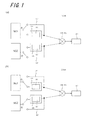
図1は、本発明の第1実施形態に係るセンサ装置100Aの原理を説明するための概略図である。(First embodiment)
FIG. 1 is a schematic diagram for explaining the principle of the
本発明の第1実施形態に係るセンサ装置100Aは、図1に示すように、第1信号発生器SG1、第2信号発生器SG2、検出素子110、リファレンス素子120、第1接続配線115、第2接続配線125、計算部140および計測部150を有する。
As shown in FIG. 1, the
(第1信号発生器SG1)
第1信号発生器SG1は、第1周波数の信号f1および第1周波数とは異なる第2周波数の信号f2のうち少なくとも一方を発生するものである。但し、第1信号発生器SG1は、第1周波数の信号f1および第2周波数の信号f2に限定されるものではなく、第3周波数の信号など、それ以外の周波数の信号を発生できるものであってもよい。(First signal generator SG1)
The first signal generator SG1 generates at least one of the first frequency signal f1 and the second frequency signal f2 different from the first frequency. However, the first signal generator SG1 is not limited to the first frequency signal f1 and the second frequency signal f2, but can generate signals of other frequencies such as a third frequency signal. May be.
本実施形態において、第1信号発生器SG1は、第1接続配線115および検出素子110のいずれかに選択的に接続可能である。そして、図1(a)に示すように、第1接続配線115に接続した状態で第1周波数の信号f1を発生し、図1(b)に示すように、検出素子110に接続した状態で第1周波数の信号f1を発生する。
In the present embodiment, the first signal generator SG1 can be selectively connected to either the
(第2信号発生器SG2)
第2信号発生器SG2は、第1周波数の信号f1および第2周波数の信号f2のうち少なくとも一方を発生するものである。但し、第1信号発生器SG1と同様に、第2信号発生器SG2は、第1周波数の信号f1および第2周波数の信号f2に限定されるものではなく、第3周波数の信号など、それ以外の周波数の信号を発生できるものであってもよい。(Second signal generator SG2)
The second signal generator SG2 generates at least one of the first frequency signal f1 and the second frequency signal f2. However, like the first signal generator SG1, the second signal generator SG2 is not limited to the first frequency signal f1 and the second frequency signal f2, but other signals such as a third frequency signal. It is also possible to generate a signal having a frequency of.
本実施形態において、第2信号発生器SG2は、第2接続配線125およびリファレンス素子120のいずれかに選択的に接続可能である。そして、図1(a)に示すように、第2接続配線125に接続した状態で第2周波数の信号f2を発生し、図1(b)に示すように、リファレンス素子120に接続した状態で第1周波数の信号f1を発生する。
In the present embodiment, the second signal generator SG2 can be selectively connected to either the
ここで、少なくとも第1信号発生器SG1および第2信号発生器SG2のうちいずれか一方の信号発生器は、第1周波数の信号f1および第2周波数の信号f2の両方を発生することができる。他方の信号発生器は、第1周波数の信号f1および第2周波数の信号f2のいずれか一方の信号のみを発生すればよい。本実施形態においては、図1(a)および図1(b)に示すように、第1信号発生器SG1は第1周波数の信号f1のみを発生し、第2信号発生器SG2は第1周波数の信号f1および第2周波数の信号f2の両方を発生する構成を採用している。 Here, at least one of the first signal generator SG1 and the second signal generator SG2 can generate both the first frequency signal f1 and the second frequency signal f2. The other signal generator may generate only one of the first frequency signal f1 and the second frequency signal f2. In the present embodiment, as shown in FIGS. 1A and 1B, the first signal generator SG1 generates only the signal f1 having the first frequency, and the second signal generator SG2 has the first frequency. The configuration that generates both the signal f1 and the signal f2 of the second frequency is employed.
(検出素子110)
検出素子110は、本実施形態において必須ではないが(後述する各センサ装置においても同様である。)、検体中に存在する標的が吸着する、またはこの標的は吸着しないが、標的との反応に応じて質量が変化する検出部111を有する。(Detecting element 110)
Although the
この検出部111は、例えば、検体の導電率などの電気的性質の影響を受けない金(Au)の膜に、標的を特異的に吸着させるような反応性を有する反応基を固定化することで実現できる。例えば、標的に特異的に結合するDNA、RNAまたは抗体等をAu膜上に固定化してもよい。このような構成により、標的の量に応じて検出部111の質量が変化するものとなる。なお、標的自体を吸着させなくても標的と特異的に反応し、反応によって検出部111の質量が変化するものであればよい。例えば、Auの膜に、標的に対して反応し、検体中に存在する標的以外の物質と反応しないような特性を有する反応基を固定化してもよい。なお、このAu膜は電気的に接地されていることが好ましい。このような構成により、標的の量に応じて検出部111の質量が変化するものとなる。
For example, the
本実施形態において、検出素子110は、第1信号発生器SG1に接続可能であり、図1(a)では接続しておらず、図1(b)では接続している。
In the present embodiment, the
そして、図1(b)に示すように、第1信号発生器SG1に検出素子110が接続した状態で、第1信号発生器SG1から検出素子110に入力信号が与えられる。このように検出素子110に与えられた入力信号が、検出部111を通過する際に、検出部111の質量変化などに応じた変化を受けて、検出信号として出力される。
Then, as shown in FIG. 1B, an input signal is given from the first signal generator SG1 to the
(リファレンス素子120)
リファレンス素子120は、本実施形態において必須ではないが(後述する各センサ装置においても同様である。)、検体中に存在する標的を吸着しない、または標的と反応しないリファレンス部121を有する。リファレンス素子120からの出力は、検出素子110からの出力に対する基準値として用いる。(Reference element 120)
Although the
このリファレンス部121は、例えば、検体中に存在する標的に対して特異的に吸着させたり、構造変化を生じて検体中の物質と置換反応を起こしたりするような反応性を有さないものである。具体的には、上述の反応基を固定化していないAuの膜あるいは上述の反応基と同程度の物質量を有し、ランダムな塩基配列を有するDNA、RNA等をAu膜上に固定化したものを用いることができる。このような構成により、リファレンス部121が標的の量に依存して質量変化を生じることを抑制できる。
For example, the
本実施形態において、リファレンス素子120は、第2信号発生器SG2に接続可能であり、図1(a)では接続しておらず、図1(b)では接続している。
In the present embodiment, the
そして、図1(b)に示すように、第2信号発生器SG2にリファレンス素子120が接続した状態で、第2信号発生器SG2からリファレンス素子120に入力信号が与えられる。このようにリファレンス素子120に与えられた入力信号が、リファレンス部121を通過する際に、リファレンス部121に応じた変化を受けて、リファレンス信号として出力される。
Then, as shown in FIG. 1B, an input signal is applied from the second signal generator SG2 to the
以上のようにして得られた検出信号およびリファレンス信号は交流信号であり、リファレンス信号は検出信号に対する基準としての役割を果たす。 The detection signal and the reference signal obtained as described above are AC signals, and the reference signal serves as a reference for the detection signal.
(第1接続配線115)
第1接続配線115は、第1信号発生器SG1に計算部140を接続する役割を有するものである。(First connection wiring 115)
The
本実施形態において、第1接続配線115は、図1(a)に示すように計算部140に接続されているとともに、第1信号発生器SG1には図1(a)および図1(b)に示すように選択的に接続される。
In the present embodiment, the
そして、図1(a)に示すように、第1接続配線115を介して第1信号発生器SG1に計算部140を接続した状態で、第1信号発生器SG1から第1周波数の信号f1を発生させることによって、計算部140は第1基準信号を得る。
Then, as shown in FIG. 1A, in a state where the
(第2接続配線125)
第2接続配線125は、第2信号発生器SG2に計算部140を接続する役割を有するものである。(Second connection wiring 125)
The
本実施形態において、第2接続配線125は、図1(a)に示すように計算部140に接続されているとともに、第2信号発生器SG2には図1(a)および図1(b)に示すように選択的に接続される。
In the present embodiment, the
そして、図1(a)に示すように、第2接続配線125を介して第2信号発生器SG2に計算部140を接続した状態で、第2信号発生器SG2から第2周波数の信号f2を発生させることによって、計算部140は第2基準信号を得る。
Then, as shown in FIG. 1A, in a state where the
(計算部140)
計算部140は、第1信号発生器SG1および第2信号発生器SG2から発生された信号に基づいて、基準電圧を算出することができるものである。計算部140は、例えばミキサとローパスフィルタとで構成することができる。(Calculation unit 140)
The
具体的には、本実施形態において、計算部140は、図1(a)に示すように、第1信号発生器SG1に第1接続配線115を介して接続した状態で、第1信号発生器SG1から第1周波数の信号f1を発生して得られる第1基準信号と、第2信号発生器SG2と第2接続配線125を介して接続した状態で、第2信号発生器SG2から第2周波数の信号f2を発生して得られる第2基準信号とを受ける。そして、これらの第1基準信号および第2基準信号から基準位相差が生じるとともに、第1基準信号および第2基準信号からヘテロダイン方式によって上述の基準位相差に対応する基準電圧を算出することができる。
このように、本実施形態に係るセンサ装置100Aによれば、センサ装置自体で簡易に基準電圧を得ることができる。それ故、例えば、基準電圧を算出した後に信号発生器を素子などに接続して検出電圧の測定を行なう場合において、装置自体の温度などの環境特性に起因する測定ばらつき、ならびに素子特性に起因する信号の大きさおよび周波数のばらつきの発生を低減することが可能となる。Specifically, in the present embodiment, the
Thus, according to the
例えば、出荷時などに基準位相差およびそれに対する基準電圧を算出したデータをセンサ装置100Aの計算部140などに格納しておくことができる。これによれば、当該データと、測定直前に改めて基準位相差およびそれに対する基準電圧を算出した値とを比較することによって、センサ装置100Aの状態(正常か故障しているか)を診断することが可能となる。このような構成、機能および効果については、後述する各センサ装置においても同様に備えるようにすることができる。
For example, data obtained by calculating a reference phase difference and a reference voltage for the reference phase difference at the time of shipment or the like can be stored in the
また、上述のような、検出素子110およびリファレンス素子120を用いて測定する場合には、これらの検出素子110およびリファレンス素子120の特性データに応じて、第1信号発生器SG1および第2信号発生器SG2から発生する信号の周波数および信号の大きさを設定すればよい。このような条件にて、基準位相差およびそれに対応する基準電圧を算出することによって、素子特性に起因する信号の大きさおよび周波数のばらつきの発生を低減することが可能となる。このような構成、機能および効果については、後述する各センサ装置においても同様に備えるようにすることができる。
When measurement is performed using the
また、計算部140は、検出素子110およびリファレンス素子120に接続することによって、検出電圧を算出することもできる。
Further, the
具体的には、計算部140は、図1(b)に示すように、第1信号発生器SG1および検出素子110に接続した状態で、第1信号発生器SG1から第1周波数の信号f1を発生して得られる第1検出信号と、第2信号発生器SG2およびリファレンス素子120に接続した状態で、第2信号発生器SG2から第1周波数の信号f1を発生して得られる第2検出信号(第1リファレンス信号)とを受ける。そして、これらの第1検出信号および第1リファレンス信号からヘテロダイン方式によって検出電圧を算出することができる。
Specifically, as shown in FIG. 1B, the
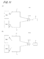
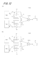
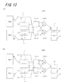
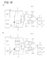
なお、図1(a)の状態において、計算部140が、検出素子110およびリファレンス素子120に接続しないようにしてもよい。これによれば、検出素子110およびリファレンス素子120により浮遊容量などが発生することによって、正確な測定を妨げるということを効果的に抑制することができる。このような接続状態を示す例としては、例えば、図11(a)、図12(a)、図13(a)および図14(a)が挙げられる。また、図1(b)の状態において、計算部140が、第1接続配線115および第2接続配線125に接続しないようにしてもよい。これによれば、第1接続配線115および第2接続配線125により寄生インダクタなどが発生することによって、正確な測定を妨げるということを効果的に抑制することができる。このような接続状態を示す例としては、例えば、図11(b)、図12(b)、図13(b)および図14(b)が挙げられる。
In the state of FIG. 1A, the
(計測部150)
計測部150は、本実施形態において必須ではないが(後述する各センサ装置においても同様である。)、上述の基準電圧を参照して、上述の検出電圧に対応する複数の位相候補値を算出するとともに、複数の位相候補値のうちの1つである検出位相差を選択するものである(後述する選択部160の役割も有している。)。(Measurement unit 150)
The
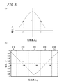
具体的には、計算部140において、ヘテロダイン方式によって検出電圧を処理しているため、図5に示すように、検出電圧は正弦曲線となり、電圧の強度(出力値)y1に相当する位相候補値として2つの値x1、x2が存在することとなる。この位相候補値とは、検出信号とリファレンス信号とにおける検出位相差を示すものである。
Specifically, since the
そして、本実施形態では、検出位相差の選択方法として、まず検出電圧からヘテロダイン方式により位相候補値を算出する。ここで、ヘテロダイン方式により検出電圧を処理しているため、信号は、0°を挟んで正負対称の正弦曲線となり、位相候補値には正負2つの値が存在することとなる。次に、検出電圧の時間的変化を確認する。検出素子110は、質量が単調変化するという特性を有するため、時間の経過と共に検出電圧に対する位相は単調変化する。この特性を利用して、例えば、検出電圧の強度が増加すれば負の位相差であり、減少すれば正の位相差であることが分かる。すなわち、検出電圧の時間的変化を確認することで、位相差の正負を判定することができる。このように、本実施形態に係るセンサ装置100Aによれば、2つの位相候補値から1つの検出位相差を決定することができる。
In this embodiment, as a method for selecting the detected phase difference, first, the phase candidate value is calculated from the detected voltage by the heterodyne method. Here, since the detection voltage is processed by the heterodyne method, the signal becomes a sine curve that is symmetric with respect to 0 °, and the phase candidate value has two values, positive and negative. Next, the temporal change of the detection voltage is confirmed. Since the
なお、後述する第2実施形態に係るセンサ装置100Bのように、検出量算出部170を有する構成にしてもよく、その場合には、上述のようにして選択された検出位相差に基づいて検体の検出量を算出することができる。このように構成することにより、検体が備える標的の検出量を算出可能なセンサ装置を提供することができる。
It should be noted that, as in the
また、本実施形態に係るセンサ装置100Aは、基準電圧の算出および検出電圧の算出において、ヘテロダイン方式によって信号を処理しているが、これに限らず、基準電圧の算出および検出電圧の算出を直交変調方式など他の方式によって信号を処理してもよい。ヘテロダイン方式によって信号を処理する構成であれば、検出信号とリファレンス信号との差分をとる計算部、すなわちミキサおよびローパスフィルタを追加するのみで検体検出量を算出可能である。このため、SAWセンサなどで位相差の測定に用いられる直交変調方式と比較して、信号処理の簡素化が可能であり、必要部品点数を少なく、小型化が可能であり、かつ消費電流を抑制することができる。
Further, the
(第2実施形態)
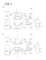
本発明の第2実施形態に係るセンサ装置100Bは、図2に示すように、第1信号発生器SG1、第2信号発生器SG2、検出素子110、リファレンス素子120、第1接続配線115、第2接続配線125、分岐部130、計算部140、計測部150、選択部160および検出量算出部170を有する。(Second Embodiment)
As shown in FIG. 2, the
本実施形態に係るセンサ装置100Bは、第1実施形態に係るセンサ装置100Aと比較して、分岐部130、選択部160および検出量算出部170をさらに有するとともに、計算部140は、第1計算部141および第2計算部142を有する。
Compared to the
以下の説明において、第1実施形態に係るセンサ装置100Aと同様の構成については説明を省略する場合がある。
In the following description, description of the same configuration as the
(第1接続配線115)
第1接続配線115は、第1信号発生器SG1に第1分岐部131を接続する役割を有するものである。すなわち、本実施形態では、第1接続配線115は、第1信号発生器SG1に、第1分岐部131を介して、第1計算部141を接続している。(First connection wiring 115)
The
本実施形態において、第1接続配線115は、図2(a)に示すように第1分岐部131に接続されているとともに、第1信号発生器SG1には図2(a)および図2(b)に示すように選択的に接続される。
In the present embodiment, the
(第2接続配線125)
第2接続配線125は、第2信号発生器SG2に第2分岐部132を接続する役割を有するものである。すなわち、本実施形態では、第2接続配線125は、第2信号発生器SG2に、第2分岐部132を介して、第2計算部142を接続している。(Second connection wiring 125)
The
本実施形態において、第2接続配線125は、図2(a)に示すように第2分岐部132に接続されているとともに、第2信号発生器SG2には図2(a)および図2(b)に示すように選択的に接続される。
In the present embodiment, the
(分岐部130)
本実施形態において、分岐部130は、第1分岐部131および第2分岐部132を有する。第1分岐部131および第2分岐部132は、例えばスプリッタで構成することができ、その一方のスプリッタによって分岐された2つの信号の位相を互いにずらすことができる。(Branch 130)
In the present embodiment, the
まず、図2(a)に示すような接続状態で、第1分岐部131および第2分岐部132によって、第1基準信号および第2基準信号を得る。具体的には次の通りである。
First, the first reference signal and the second reference signal are obtained by the
第1分岐部131は、図2(a)に示すように、第1接続配線115によって第1信号発生器SG1に第1分岐部131を接続した状態で、第1信号発生器SG1から第1周波数の信号f1を発生させることによって、第1基準信号を得る。そして、この第1基準信号を第1分岐信号と第2分岐信号とに分岐する。ここで、第1分岐信号と第2分岐信号とは位相の同じ信号である。すなわち、第1基準信号を2つの同一信号Aに分岐するものである。
As shown in FIG. 2A, the
第2分岐部132は、図2(a)に示すように、第2接続配線125によって第2信号発生器SG2に第2分岐部132を接続した状態で、第2信号発生器SG2から第2周波数の信号f2を発生させることによって、第2基準信号を得る。そして、この第2基準信号を第3分岐信号と第4分岐信号とに分岐する。ここで、第3分岐信号は、第1分岐信号と同じ位相である。第4分岐信号は、第3分岐信号から位相をずらしている。ただし、位相をずらす値としては180°を除く。この例では90°位相をずらしている。図2中において、第3分岐信号をBで、第4分岐信号をB’で表している。これによれば、第4分岐信号の位相を第1〜第3分岐信号に対して90°ずらしていることより、第1検出電圧が最も感度が低くなるときに、第2検出電圧が最も感度の高い領域となるため、高感度にすることができる。
As shown in FIG. 2A, the
なお、本実施形態に係るセンサ装置100Bでは、リファレンス信号を第3分岐信号と第4分岐信号とに位相をずらして分岐した例を示したが、これに代えて、検出信号から位相をずらして分岐した信号を出力するようにしてもよい。また、第4分岐信号の位相を第1分岐信号に対して90°ずらした例を説明したが、180°を除く値であれば90°以外でもよい。
In the
なお、例えば、第1分岐部131で、信号を2つに分岐させて同一位相の分岐信号を得るとともに、第2分岐部132で、信号を2つに分岐させた後に、一方の線路長を他方の線路長に対して異ならせることによって、分岐信号間で位相をずらすようにしてもよい。
For example, the
ここで、分岐部130(第1分岐部131および第2分岐部132)において各分岐信号における位相のずれは、後述の第1計算部141において、第1分岐信号Aから第3分岐信号Bを差し引いた値として算出される第1基準位相差と、後述の第2計算部142において、第2分岐信号Aから第4分岐信号B’を差し引いた値として算出される第2基準位相差とが異なる値になるように設定される。このような位相のずれの設定については、他の分岐部130、および他の実施形態におけるセンサ装置100においても同様である。
Here, in the branching unit 130 (the first branching
次に、図2(b)に示すような接続状態で、第1分岐部131および第2分岐部132によって、上述の基準信号と同様にして、検出信号およびリファレンス信号を得る。具体的には次の通りである。
Next, in the connection state as shown in FIG. 2B, the detection signal and the reference signal are obtained by the
第1分岐部131は、図2(b)に示すように、第1接続配線115を用いずに、第1信号発生器SG1、検出素子110および第1分岐部131を接続した状態で、第1信号発生器SG1から第1周波数の信号f1を発生させることによって、検出信号を得る。そして、この検出信号を第1分岐信号と第2分岐信号とに分岐する。ここで、第1分岐信号と第2分岐信号とは位相の同じ信号である。すなわち、検出信号を2つの同一信号に分岐するものである。図2中において、第1分岐信号および第2分岐信号をいずれも符号Aで表している。
As shown in FIG. 2B, the
第2分岐部132は、図2(b)に示すように、第2接続配線125を用いずに、第2信号発生器SG2、リファレンス素子120および第2分岐部132を接続した状態で、第2信号発生器SG2から第1周波数の信号f1を発生させることによって、リファレンス信号を得る。そして、このリファレンス信号を第3分岐信号と第4分岐信号とに分岐する。ここで、第3分岐信号は、第1分岐信号と同じ位相である。第4分岐信号は、第1分岐信号から位相を、180°を除く値だけずらしている。この例では90°位相をずらしている。図2中において、第3分岐信号を符号Bで、第4分岐信号を符号B’で表している。
As shown in FIG. 2B, the
(計算部140)
本実施形態において、計算部140は、第1計算部141と第2計算部142とを有する。(Calculation unit 140)
In the present embodiment, the
計算部140は、上述の第1基準信号あるいは検出信号を分岐した第1分岐信号Aおよび第2分岐信号Aと、第2基準信号あるいはリファレンス信号を分岐した第3分岐信号Bおよび第4分岐信号B’とから、例えばヘテロダイン方式によって基準電圧あるいは検出電圧を得る。基準電圧および検出電圧のいずれを得るかは、信号発生器と素子との接続の有無に応じて決まる。第1計算部141および第2計算部142は、例えばミキサとローパスフィルタとで構成することができる。
The
具体的には、上述の通り、図2(a)に示すように各構成要素を接続した状態において、第1計算部141は、第1分岐信号Aから第3分岐信号Bを差し引いた値である第1基準位相差を得て、ヘテロダイン方式によってこの第1基準位相差に対応する第1基準電圧を得るとともに、第2計算部142は、第2分岐信号Aから第4分岐信号B’ を差し引いた値である第2基準位相差を得て、ヘテロダイン方式によってこの第2基準位相差に対応する第2基準電圧を算出する。
Specifically, as described above, in the state where the respective components are connected as shown in FIG. 2A, the
また、図2(b)に示すように各構成要素を接続した状態において、第1計算部141は、第1分岐信号Aから第3分岐信号Bを差し引いた値である第1検出位相差を得て、ヘテロダイン方式によってこの第1検出位相差に対応する第1検出電圧を得るとともに、第2計算部142は、第2分岐信号Aから第4分岐信号B’ を差し引いた値である第2検出位相差を得て、ヘテロダイン方式によってこの第2検出位相差に対応する第2検出電圧を算出する。
Further, in the state where the respective components are connected as shown in FIG. 2B, the
このように、本実施形態に係るセンサ装置100Bによれば、2つの信号発生器と2つの計算部との接続構成を変更しつつ、2つの信号発生器から所定の周波数の信号を発生することによって、センサ装置自体で簡易に図6(a)に示すような基準電圧を算出することができる。その他、上述の第1実施形態に係るセンサ装置100Aと同様の効果を奏することができる。
As described above, according to the
(計測部150)
計測部150は、第1検出電圧から2つの第1位相候補値を算出し、そのうちの一方を第1検出位相差と判断する。同様に、第2検出電圧から2つの第2位相候補値を算出し、そのうち一方を第2検出位相差と判断する。(Measurement unit 150)
The
ここで、本実施形態においても、ヘテロダイン方式によって第1検出電圧および第2検出電圧を処理しているため、第1検出電圧および第2検出電圧はそれぞれ図5(a)に示すような正弦曲線となり、電圧の強度(出力値)y1に相当する位相候補値として2つの値x1、x2が存在することとなる。位相候補値とは、検出信号とリファレンス信号とにおける検出位相差を示すものである。 Here, also in this embodiment, since the first detection voltage and the second detection voltage are processed by the heterodyne method, the first detection voltage and the second detection voltage are respectively sinusoidal curves as shown in FIG. Thus, there are two values x1 and x2 as phase candidate values corresponding to the voltage intensity (output value) y1. The phase candidate value indicates a detection phase difference between the detection signal and the reference signal.
具体的に第1検出電圧および第2検出電圧に対して検討すると、第1検出電圧に対して2つの第1位相候補値x11、x21が存在する。同様に第2検出電圧に対して2つの第2位相候補値x12、x22が存在する。ここで、x11とx12との組合せ、x11とx22との組合せ、x21とx12との組合せ、およびx21とx22との組合せの合計4つの組合せの中で、最も値(位相差の値)が近いもので組合せを構成する位相候補値をそれぞれ、第1検出電圧に対応する第1検出位相差および第2検出電圧に対応する第2検出位相差とする。すなわち、4つの組合せのそれぞれについて差を求め、その値が最も小さくなる組合せを選択する。そして、選択した組合せをなす位相候補値をそれぞれ、第1検出電圧に対応する第1検出位相差および第2検出電圧に対応する第2検出位相差とする。これは、以下のメカニズムによる。 Specifically, when considering the first detection voltage and the second detection voltage, there are two first phase candidate values x11 and x21 for the first detection voltage. Similarly, there are two second phase candidate values x12 and x22 for the second detection voltage. Here, the combination of x11 and x12, the combination of x11 and x22, the combination of x21 and x12, and the combination of x21 and x22 has the closest value (phase difference value). The phase candidate values constituting the combination with the first detection phase difference are the first detection phase difference corresponding to the first detection voltage and the second detection phase difference corresponding to the second detection voltage. That is, the difference is obtained for each of the four combinations, and the combination having the smallest value is selected. And let the phase candidate value which makes the selected combination be the 1st detection phase difference corresponding to the 1st detection voltage, and the 2nd detection phase difference corresponding to the 2nd detection voltage, respectively. This is due to the following mechanism.
すなわち、理論上では、第1基準電圧の2つの第1位相候補値のうちの1つと、第2基準電圧の2つの第2位相候補値のうちの1つとが同じになる。この同じ値が正しい位相差(第1基準位相差、第2基準位相差)である。しかしながら、実測定である第1検出電圧および第2検出電圧においては、誤差によって完全に同一の値をとることができない可能性がある。このため、差が最も少ない組合せ(すなわち最も近い値を取るもの)を正しい位相差であるとして、第1検出位相差および第2検出位相差と判別するものである。 That is, theoretically, one of the two first phase candidate values of the first reference voltage is the same as one of the two second phase candidate values of the second reference voltage. This same value is the correct phase difference (first reference phase difference, second reference phase difference). However, in the first detection voltage and the second detection voltage that are actual measurements, there is a possibility that the same value cannot be obtained due to an error. Therefore, the combination having the smallest difference (that is, the one having the closest value) is determined as the correct phase difference, and is determined as the first detection phase difference and the second detection phase difference.
(選択部160)
選択部160は、計測部150にて得られた第1検出位相差および第2検出位相差から、1つの検出位相差を選択する。(Selection unit 160)
The
具体的には、上述のようにして得られた第1検出位相差および第2検出位相差のうち信号の出力値(例えば、V1、V2)が所定の基準値に近い方を検出位相差として選択する。これによれば、所定の基準値を基準として選択すべき検出位相差を特定することができる。ここで、基準値として、例えば、0(ゼロ)あるいは2つの交点強度の中点などを設定することができる。図6に示すような理論的な軌跡を用いる場合には、基準値である2つの交点強度の中点はゼロになる。なお、基準値としては、2つの交点強度の中点に限られず、第1検出電圧および第2検出電圧を考慮して、高い感度の検出電圧を得ることができるよう適切な値に設定すればよい。 Specifically, of the first detection phase difference and the second detection phase difference obtained as described above, a signal output value (for example, V1, V2) closer to a predetermined reference value is set as a detection phase difference. select. According to this, it is possible to specify a detection phase difference to be selected with a predetermined reference value as a reference. Here, as the reference value, for example, 0 (zero) or the midpoint of the two intersection strengths can be set. When a theoretical trajectory as shown in FIG. 6 is used, the midpoint between the two intersection strengths which are the reference values is zero. Note that the reference value is not limited to the middle point between the two intersection strengths, and can be set to an appropriate value so that a highly sensitive detection voltage can be obtained in consideration of the first detection voltage and the second detection voltage. Good.
このように、本実施形態によれば、上述のようにヘテロダイン方式によって2つの検出信号(第1および第2検出信号)を用いて信号処理を行なうことから、位相候補値から位相差を判断することができる。それ故、1つの検出信号を用いる場合と比較して、広い位相範囲において測定することが可能となる。 As described above, according to the present embodiment, since the signal processing is performed using the two detection signals (first and second detection signals) by the heterodyne method as described above, the phase difference is determined from the phase candidate value. be able to. Therefore, it is possible to measure in a wider phase range than in the case of using one detection signal.
(検出量算出部170)
検出量算出部170は、選択部160に接続されている。(Detection amount calculation unit 170)
The detection
検出量算出部170において、選択部160にて選択された検出位相差を用いて、検体の検出量を算出する。例えば、検出量算出部170は、予め標準検体の検出量に関するデータを有しており、当該データと実測定で得られた値とを対比することによって、検体の検出量を算出することができる。
The detection
以上のような構成を有することにより、検体が備える標的の検出量を算出可能なセンサ装置を提供することができる。 With the above-described configuration, it is possible to provide a sensor device that can calculate the detection amount of the target included in the specimen.
以上のような、本実施形態に係るセンサ装置100Bによれば、上述の第1実施形態に係るセンサ装置100Aと同様の効果を奏することができる。
それに加えて、以下のような効果を有する。According to the
In addition, it has the following effects.
まず、通常のヘテロダイン方式では位相差の正負の判断が付かないため、測定可能な位相範囲は0°から180°までの範囲のみであった。これに対して、本実施形態に係るセンサ装置100Bによれば、第1検出電圧および第2検出電圧を第1位相候補値および第2位相候補値と比較することによって、位相候補値からの位相の正負を判断し、検出位相差を推定することができる。これにより、測定可能な位相範囲を−180°から180°まで広げることができる。さらに、連続的に第1検出電圧および第2検出電圧の電圧強度の変化を測定することによって、180°を超える位相範囲においても測定可能となる。
First, in the normal heterodyne method, whether the phase difference is positive or negative cannot be determined, and therefore the measurable phase range is only the range from 0 ° to 180 °. On the other hand, according to the
また、通常のヘテロダイン方式では、検出電圧は正弦曲線を描くため、位相差が0°および±180°で傾きが小さくなり、感度が低くなったり誤差が大きくなったりするおそれがある。これに対して、本実施形態に係るセンサ装置100Bによれば、傾きが小さくなる領域を省き、全ての位相範囲で傾きの大きい検出電圧を用いることとなる。これにより、位相変化に対して電圧変化率の高いものとすることができ、高感度にすることができる。特に、センサ装置において、位相差0°付近は、標的検出による信号変化の立ち上り部分に相当することが多く、高い感度で測定することが望まれることから、本実施形態に係るセンサ装置100Bは、優れた効果を発揮することができる。
Further, in the normal heterodyne system, the detection voltage draws a sinusoidal curve, so that the slope becomes small when the phase difference is 0 ° and ± 180 °, and there is a possibility that the sensitivity becomes low and the error becomes large. On the other hand, according to the
さらに、上述のような2つの検出電圧(第1検出電圧、第2検出電圧)を用いることより、ノイズ判定を行なうことができる。これは以下のようなメカニズムによる。検出信号およびリファレンス信号にはノイズが混入することがあるが、通常はこのようなノイズをノイズとして判別することは困難である。これに対して、本実施形態に係るセンサ装置100Bによれば、ノイズが混入せず正しく測定できている場合には、第1検出電圧および第2検出電圧の一方の電圧強度が交点強度VmaxおよびVminの間の範囲に入る値をとり、他方がこの範囲を外れる値をとる。言い換えると、第1検出電圧および第2検出電圧のいずれもが、この範囲内の値をとったりこの範囲外の値をとったりする場合には、ノイズであると判断することができる。このようにして、ノイズを判別することができるので、例えば、ノイズが混入したと判断した場合には、その測定結果を採用せず、再度測定をやり直すなどすることで、ノイズに影響されずに、より正確な測定をすることが可能となる。
Furthermore, noise determination can be performed by using the two detection voltages (first detection voltage and second detection voltage) as described above. This is due to the following mechanism. Although noise may be mixed in the detection signal and the reference signal, it is usually difficult to determine such noise as noise. On the other hand, according to the
(第2実施形態の変形例)
ここで、上述の第2実施形態に係るセンサ装置100Bにおいて、計測部150および選択部160の内容が異なる変形例を以下において説明する。それ以外の構成については、第2実施形態に係るセンサ装置100Bと同一である。以下、本変形例における計測部150’および選択部160’について詳細に説明する。(Modification of the second embodiment)
Here, in the
(計測部150’)
計測部150’は、第1検出電圧から2つの第1位相候補値を算出し、そのうちの一方を第1検出位相差と判断する。同様に、第2検出電圧から2つの第2位相候補値を算出し、そのうち一方を第2検出位相差と判断する。(
The
具体的には、予め第1検出電圧と第2検出電圧との位相差に対する軌跡を求め、第1検出電圧と第2検出電圧との交点における正負2つの強度を求める。そして、第1検出電圧と第2検出電圧とのうち、交点における正負2つの強度の間に位置するものを検出電圧として選択する。具体的には、以下の通りである。 Specifically, a locus for the phase difference between the first detection voltage and the second detection voltage is obtained in advance, and two intensities of positive and negative at the intersection of the first detection voltage and the second detection voltage are obtained. Then, the first detection voltage and the second detection voltage that are located between two positive and negative intensities at the intersection are selected as detection voltages. Specifically, it is as follows.
図6(a)は、第1検出電圧および第2検出電圧の理論値の軌跡を示す図である。本実施形態においては、図6(a)における第1検出電圧の理論値を第1基準電圧と見做し、第2検出電圧の理論値を第2基準電圧と見做して、それを基準として実測定を行なって検体をセンシングすればよい。便宜上、第1検出電圧の強度をV1とし、第2検出電圧の強度をV2とし、第1検出電圧の軌跡と第2検出電圧の軌跡との交点の強度を大きい値から順にVmaxおよびVminとしている。また、第1検出電圧の軌跡を破線で、第2検出電圧の軌跡を実線で示している。理論的には、交点の強度VmaxおよびVminは、V1およびV2の最大強度の0.5倍および−0.5倍となる。 FIG. 6A is a diagram illustrating a locus of theoretical values of the first detection voltage and the second detection voltage. In the present embodiment, the theoretical value of the first detection voltage in FIG. 6A is regarded as the first reference voltage, the theoretical value of the second detection voltage is regarded as the second reference voltage, and is used as a reference. The actual measurement may be performed to sense the specimen. For convenience, the intensity of the first detection voltage is V1, the intensity of the second detection voltage is V2, and the intensity of the intersection of the locus of the first detection voltage and the locus of the second detection voltage is Vmax and Vmin in descending order. . Further, the locus of the first detection voltage is indicated by a broken line, and the locus of the second detection voltage is indicated by a solid line. Theoretically, the intersection strengths Vmax and Vmin are 0.5 times and -0.5 times the maximum strength of V1 and V2.
ここで、第1検出電圧および第2検出電圧がいずれかの交点の強度をとる位相値ごとに位相値の区間を区切る。図6(a)では区間1〜区間5を示している。なお、区間1〜区間4を繰り返すものであり、区間1と区間5とは同一となる。そして、区間1では第2検出電圧を、区間2では第1検出電圧を、区間3では第2検出電圧を、区間4では第1検出電圧を、区間5では第2検出電圧をそれぞれ検出電圧として選択する。これを言い換えると、次のようになる。
V1>V2、且つV1>Vmax・・・検出電圧としてV2を採用
V1<V2、且つV2>Vmax・・・検出電圧としてV1を採用
V1<V2、且つV1<Vmin・・・検出電圧としてV2を採用
V1>V2、且つV2<Vmin・・・検出電圧としてV1を採用
仮にV1=V2の場合は、どちらを検出電圧として採用してもよい。Here, the section of the phase value is divided for each phase value at which the first detection voltage and the second detection voltage take the intensity of any intersection. FIG. 6A shows
V1> V2 and V1> Vmax: V2 is used as the detection voltage V1 <V2, and V2> Vmax ... V1 is used as the detection voltage V1 <V2, and V1 <Vmin ... V2 is used as the detection voltage Adoption V1> V2 and V2 <Vmin... V1 is adopted as the detection voltage. If V1 = V2, either may be adopted as the detection voltage.
以上のようにして選択した検出電圧の軌跡を、図6(b)に示す。 The locus of the detection voltage selected as described above is shown in FIG.
(選択部160’)
選択部160’は、計測部150’にて得られた第1検出位相差および第2検出位相差から、1つの検出位相差を選択する。(
The
具体的には、第1検出電圧を検出電圧としたときには、第1検出位相差を検出位相差とし、第2検出電圧を検出電圧としたときには、第2検出位相差を検出位相差とする。 Specifically, when the first detection voltage is the detection voltage, the first detection phase difference is the detection phase difference, and when the second detection voltage is the detection voltage, the second detection phase difference is the detection phase difference.
以上のようにして、選択部160’にて選択された検出位相差を用いて、第2実施形態に係るセンサ装置100Bにおける検出量算出部170と同様に、検体の検出量を算出することができる。
As described above, the detection amount of the specimen can be calculated using the detection phase difference selected by the
(第3実施形態)
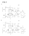
本発明の第3実施形態に係るセンサ装置100Cは、図3に示すように、第1信号発生器SG1、第2信号発生器SG2、検出素子110、リファレンス素子120、素子分岐部105、第1接続配線115、第2接続配線125、分岐部130、計算部140、計測部150、選択部160および検出量算出部170を有する。以下、上述の第1および第2実施形態に係るセンサ装置100A、100Bと同様の構成については説明を省略する場合がある。(Third embodiment)
As illustrated in FIG. 3, the
上述の実施形態に係るセンサ装置100A、100Bでは、図1および図2に示すように、第1信号発生器SG1は検出素子110に接続可能であり、第2信号発生器SG2はリファレンス素子120に接続可能な構成を有している。
In the
これに対して、本実施形態に係るセンサ装置100Cは、図3に示すように、検出素子110およびリファレンス素子120に接続している素子分岐部105を有している。そして、第1信号発生器SG1は素子分岐部105に接続せず、第2信号発生器SG2が素子分岐部105に接続可能である。
On the other hand, the
そして、図3(b)に示すように、第2信号発生器SG2から発生した信号が、素子分岐部105を介して、検出素子110およびリファレンス素子120に入力されることになる。入力された信号は、その後、上述の第2実施形態に係るセンサ装置100Bと同様の経路を辿って検出・処理される。ここで、素子分岐部105は、例えばスプリッタで構成することができる。なお、変形例として、第1信号発生器SG1および第2信号発生器SG2の一方から発生する信号を素子分岐部105を採用することなく2つに分岐し、検出素子110およびリファレンス素子120などの複数の素子に入力される構成を採用してもよい。この場合において、素子が3つ以上存在する場合には、上述のように2つに分岐された信号が、入力される2つの素子に選択的に接続することが可能なスイッチを設ければよい。
Then, as shown in FIG. 3B, the signal generated from the second signal generator SG <b> 2 is input to the
本実施形態に係るセンサ装置100Cにおいて、第1信号発生器SG1および第2信号発生器SG2から出力される信号は次の通りである。図3(a)の接続状態においては、第1信号発生器SG1から第1周波数の信号f1が、第2信号発生器SG2から第2周波数の信号f2が出力され、図3(b)の接続状態においては、第2信号発生器SG2から第1周波数の信号f1が出力されるようにすればよい。
In the
以上のように、本実施形態に係るセンサ装置100Cにおいても、上述の実施形態と同様に、第1信号発生器SG1に計算部140を接続した状態で、第1信号発生器SG1から第1周波数の信号f1を発生し、第2信号発生器SG2に計算部140を接続した状態で、第2信号発生器SG2から第2周波数の信号f2を発生することによって、センサ装置自体で簡易に基準位相差を得ることができ、この基準位相差に対応する基準電圧を算出することができる
それに加えて、本実施形態に係るセンサ装置100Cにおいても、上述の第2実施形態に係るセンサ装置100Bと同様の効果を奏することができる。As described above, also in the
(第4実施形態)
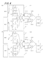
本発明の第4実施形態に係るセンサ装置100Dは、図4に示すように、第1信号発生器SG1、第2信号発生器SG2、検出素子110a、検出素子110b、リファレンス素子120a、リファレンス素子120b、素子分岐部105、第1接続配線115、第2接続配線125、分岐部130、計算部140、計測部150、選択部160および検出量算出部170を有する。以下、第1〜第3実施形態に係るセンサ装置100A〜100Cと同様の構成については説明を省略する場合がある。(Fourth embodiment)
As shown in FIG. 4, the
上述の実施形態に係るセンサ装置100A〜100Cでは、図1〜図3に示すように、検出素子110およびリファレンス素子120が1つずつであり、1つの検出素子110に第1分岐部131が接続されるとともに、1つのリファレンス素子120に第2分岐部132が接続される構成を有している。
In the
これに対して、本実施形態に係るセンサ装置100Dは、図4に示すように、検出素子110およびリファレンス素子120をそれぞれ2つとし、2つの検出素子110a、bに第1分岐部131が選択的に接続可能であるとともに、2つのリファレンス素子120a、bに第2分岐部132が選択的に接続可能である。
On the other hand, as shown in FIG. 4, the
これら2つの検出素子110a、bは、同じであっても異なっていてもよく、異なる場合には、それぞれが特異的に吸着する標的の種類が異なるように、Au膜に異なるDNA、RNA、または抗体等を固定すればよい。
These two
具体的には、第1分岐部131は、スイッチ136aによって2つの検出素子110a、bのうちのいずれかに選択的に接続できるようにし、第2分岐部132は、スイッチ136bによって2つのリファレンス素子120a、bのうちのいずれかに選択的に接続できるようにすればよい。
Specifically, the
これによれば、検体に含まれる2つ以上の検出対象を、分岐部130に続く構成(すなわち計算部140、計測部150、選択部160および検出量算出部170の構成)を変更することなく、一度に(1つの検体を用いることによって)検出することが可能となる。
According to this, two or more detection targets included in the sample are changed without changing the configuration following the branching unit 130 (that is, the configuration of the
以上のように、本実施形態に係るセンサ装置100Dにおいても、上述の実施形態と同様に、第1信号発生器SG1に計算部140を接続した状態で、第1信号発生器SG1から第1周波数の信号f1を発生し、第2信号発生器SG2に計算部140を接続した状態で、第2信号発生器SG2から第2周波数の信号f2を発生することによって、センサ装置自体で簡易に基準位相差を得ることができ、この基準位相差に対応する基準電圧を算出することができる。
As described above, also in the
それに加えて、本実施形態に係るセンサ装置100Dにおいても、上述の第2実施形態に係るセンサ装置100Bと同様の効果を奏することができる。
In addition, the
なお、上述の接続構成に代えて、図4の各スイッチ135、136の構成に示すように、例えば、第1分岐部131および第2分岐部132のそれぞれを、2つの検出素子および2つのリファレンス素子のいずれに対しても任意に接続できるようにしてもよい。
Instead of the connection configuration described above, as shown in the configuration of the switches 135 and 136 in FIG. 4, for example, each of the
また、上述の素子構成に代えて、例えば、検出素子を3つにし、リファレンス素子を1つにしてもよい。この場合において、第1分岐部および第2分岐部のいずれか一方がリファレンス素子に接続する構成であればよく、他方については3つの検出素子のいずれに接続するかは特に限定されず、検出対象の種類・数に応じて適宜設定することができる。 Further, instead of the above-described element configuration, for example, three detection elements may be provided and one reference element may be provided. In this case, any one of the first branch part and the second branch part may be configured to be connected to the reference element, and there is no particular limitation on which of the three detection elements is connected to the other, and the detection target It can be set as appropriate according to the type and number of.
(第5実施形態)
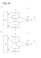
本発明の第5実施形態に係るセンサ装置101は、図15に示すように、信号発生器SG、検出素子110、リファレンス素子120、第1接続配線115、第2接続配線125、計算部140および計測部150を有する。(Fifth embodiment)
As shown in FIG. 15, the
本実施形態に係るセンサ装置101は、第1実施形態に係るセンサ装置100Aと比較して、第1信号発生器SG1および第2信号発生器SG2の2つの信号発生器を備える代わりに1つの信号発生器SGを備える点で異なっている。
Compared with the
以下の説明において、第1実施形態に係るセンサ装置100Aと同様の構成については説明を省略する場合がある。
In the following description, description of the same configuration as the
(信号発生器SG)
信号発生器SGは、第1周波数の信号f1および第1周波数とは異なる第2周波数の信号f2を発生するものである。但し、信号発生器SGは、第1周波数の信号f1および第2周波数の信号f2に限定されるものではなく、第3周波数の信号などそれ以外の周波数の信号を発生できるものであってもよい。(Signal generator SG)
The signal generator SG generates a signal f1 having a first frequency and a signal f2 having a second frequency different from the first frequency. However, the signal generator SG is not limited to the signal f1 of the first frequency and the signal f2 of the second frequency, and may be one that can generate signals of other frequencies such as a signal of the third frequency. .
本実施形態において、信号発生器SGは、第1周波数の信号f1および前記第2周波数の信号f2のうち少なくとも一方を出力する第1出力部と、第1周波数の信号f1および第2周波数の信号f2のうち少なくとも一方を出力する第2出力部とを有する。第1出力部は、第1接続配線115および検出素子110のいずれかに選択的に接続可能であり、第2出力部は、第2接続配線125および検出素子120のいずれかに選択的に接続可能である。そして、図15(a)に示すように、第1出力部が、第1接続配線115に接続した状態で第1周波数の信号f1を発生し、第2出力部が、第2接続配線125に接続した状態で第2周波数の信号f2を発生し、図15(b)に示すように、第1出力部が、検出素子110に接続した状態で第1周波数の信号f1を発生し、第2出力部が、検出素子120に接続した状態で第1周波数の信号f1を発生する。
In the present embodiment, the signal generator SG includes a first output unit that outputs at least one of the first frequency signal f1 and the second frequency signal f2, and the first frequency signal f1 and the second frequency signal. and a second output unit that outputs at least one of f2. The first output unit can be selectively connected to either the
信号発生器SGは、第1出力部および第2出力部から同時に信号を出力することができればよい。例えば、図15(a)のような接続状態では、第1出力部からは信号f1を出力し、それと同時に第2出力部からは信号f1とは周波数が異なる信号f2を出力する。図15(b)のような接続状態では、第1出力部からは信号f1を出力し、それと同時に第2出力部からも信号f1を出力する。 The signal generator SG only needs to be able to output signals simultaneously from the first output unit and the second output unit. For example, in the connection state as shown in FIG. 15A, the signal f1 is output from the first output unit, and at the same time, the signal f2 having a frequency different from that of the signal f1 is output from the second output unit. In the connection state as shown in FIG. 15B, the signal f1 is output from the first output unit, and at the same time, the signal f1 is output from the second output unit.
(センサ装置100Aの素子構成)
次に、本発明の実施形態に係るセンサ装置の原理を具体化した構成について説明する。以下では図7〜図9を用いて、実施形態の一例として、本発明の第1実施形態に係るセンサ装置100Aにおける素子(検出素子110およびリファレンス素子120)を具体化した構成について説明する。(Element structure of the
Next, the structure which actualized the principle of the sensor apparatus based on embodiment of this invention is demonstrated. Hereinafter, as an example of the embodiment, a configuration in which the elements (the
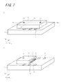
素子(検出素子110およびリファレンス素子120)は、図7(a)の斜視図に示すように、外観上は主に圧電基板1とカバー3とで構成されている。カバー3には、検体溶液の流入口である第1貫通孔18と空気孔または検体溶液の流出口である第2貫通孔19とが設けられている。
As shown in the perspective view of FIG. 7A, the elements (the
図7(b)に、カバー3の片側半分を取り除いたときのセンサ装置100Aの斜視図を示す。同図に示すように、カバー3の内部には検体(溶液)の検体用流路となる空間20が形成されている。第1貫通孔18はこの空間20に繋がっている。すなわち、第1貫通孔18から入った検体は空間20に流れ込むようになっている。
FIG. 7B is a perspective view of the
空間20に流れ込んだ検体液には標的が含まれており、その標的が圧電基板1上に形成された金属膜7などからなる検出部と反応する。
The sample liquid that has flowed into the
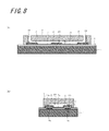
図8にセンサ装置100Aの素子(検出素子110およびリファレンス素子120)の断面図を示す。図8(a)は図7(a)のVIa−VIa線における断面図であり、図8(b)は図7(a)のVIb−VIb線における断面図である。図9に圧電基板1の上面図を示す。
FIG. 8 shows a cross-sectional view of the elements (the
図8、図9に示すように、圧電基板1の上面には、検出第1IDT電極5a、検出第2IDT電極6a、リファレンス第1IDT電極5bおよびリファレンス第2IDT電極6bが形成されている。検出第1IDT電極5aおよびリファレンス第1IDT電極5bは所定のSAWを発生させるためのものであり、検出第2IDT電極6aおよびリファレンス第2IDT電極6bは、それぞれ検出第1IDT電極5aおよびリファレンス第1IDT電極5bで発生したSAWを受信するためのものである。検出第1IDT電極5aで発生したSAWを検出第2IDT電極6aが受信できるように、検出第2IDT電極6aは、検出第1IDT電極5aで発生したSAWの伝搬路上に配置されている。リファレンス第1IDT電極5bおよびリファレンス第2IDT電極6bも同様に配置される。
As shown in FIGS. 8 and 9, a detection
検出第1IDT電極5aおよび検出第2IDT電極6aは、それぞれ配線8を介してパッド9に接続されている。これらのパッド9および配線8を介して外部から検出第1IDT電極5aに信号が入力され、検出第2IDT電極6aから外部に信号が出力される。リファレンス第1IDT電極5bおよびリファレンス第2IDT電極6bは、検出第1IDT電極5aおよび検出第2IDT電極6aと同様であるため、以下、適宜説明を省略する。
The detection
検出第1IDT電極5a、検出第2IDT電極6a、リファレンス第1IDT電極5bおよびリファレンス第2IDT電極6bは、保護膜4によって覆われている。保護膜4は各電極および配線の酸化防止などに寄与するものである。
The detection
図8(b)に示すように、検出第1IDT電極5aは第1振動空間11aに収容され、検出第2IDT電極6aは第2振動空間12aに収容されている。これにより、検出第1IDT電極5aおよび検出第2IDT電極6aが外気および検体液から隔離され、水分などの腐食物質から検出第1IDT電極5aおよび検出第2IDT電極6aを保護することができる。また、第1振動空間11aおよび第2振動空間12aが確保されることによって、検出第1IDT電極5aおよび検出第2IDT電極6aにおいてSAWの励振が大きく阻害されない状態とすることができる。
As shown in FIG. 8B, the detection
板状体2の、第1振動空間11aおよび第2振動空間12aを形成するための凹部の間には、板状体2を厚み方向に貫通している部分である貫通部が形成されている。この貫通部は、SAWの伝搬路上に金属膜7aを形成するために設けられたものである。すなわち、板状体2を圧電基板1に接合したときに、平面視で、検出第1IDT電極5aから検出第2IDT電極6aに伝搬するSAWの伝搬路の少なくとも一部が貫通部から露出し、その露出部に金属膜7aが形成される。
Between the concave portions for forming the
同様に、板状体2の、第1振動空間11bおよび第2振動空間12bを形成するための凹部の間には、板状体2を厚み方向に貫通している部分である他の貫通部が形成されている。この貫通部は、SAWの伝搬路上に金属膜7bを形成するために設けられたものである。
Similarly, between the recesses for forming the first vibration space 11b and the second vibration space 12b of the plate-
このような形状の板状体2は、例えば、感光性のレジストを用いて形成することができる。
The plate-
板状体2の貫通部から露出する金属膜7aは、検体液の検出部を構成する。金属膜7aは、例えば、クロム(Cr)層およびクロム層上に成膜された金(Au)層の2層構造となっている。金属膜7aの表面には、例えば、核酸またはペプチドからなるアプタマーが固定化されている。このようにアプタマーが固定化された金属膜7aに検体液が接触すると、検体液中の特定の標的物質がその標的物質に対応するアプタマーと結合する。このような構成とすることで、検体中の標的物質がアプタマーと結合し、吸着するにつれて金属膜7aの質量が単調増加するものとなる。すなわち、検体中の標的物質の量に応じて質量が単調増加するものとなる。なお、ここで金属膜7aの質量が単調増加するのは、検体が連続的に金属膜7a上に供給される間のみである。
The
また、板状体2の他の貫通部から露出する金属膜7bは、リファレンス部を構成する。金属膜7bは、例えば、クロム層およびクロム層上に成膜された金層の2層構造となっている。金属膜7aの表面には、検体に対して反応性を示さないように、金属膜7aに固定化したようなアプタマーを付けないものとする。さらに、検体溶液に対して反応性を低めて安定化させるような表面処理を行なってもよい。
Further, the
SAWを利用して検体溶液の性質などを測定するには、まず、検出第1IDT電極5aに、パッド9および配線8を介して外部の測定器から所定の電圧(信号)を印加する。そうすると、検出第1IDT電極5aの形成領域において圧電基板1の表面が励振され、所定の周波数を有するSAWが発生する。発生したSAWはその一部が検出第1IDT電極5aと検出第2IDT電極6aとの間の領域を通過し、検出第2IDT電極6aに到達する。このとき金属膜7aでは、金属膜7aに固定化されたアプタマーが検体中の特定の標的物質と結合し、結合した分だけ金属膜7aの重さ(質量)が変化することになるため、金属膜7aの下を通過するSAWの位相特性などが変化する。このように特性が変化したSAWが検出第2IDT電極6aに到達すると、それに応じた電圧が検出第2IDT電極6aに生じる。この電圧が交流信号の検出信号として配線8およびパッド9を介して外部に出力され、それを図1に示す分岐部130および計算部140を経て処理することによって、検体液の性質または成分を調べることができる。
In order to measure the property of the sample solution using SAW, first, a predetermined voltage (signal) is applied to the detection
すなわち、圧電基板1と、圧電基板1上に形成された検出部としての金属膜7aと、検出第1IDT電極5aおよび検出第2IDT電極6aとで検出素子110Aを構成する。
That is, the
同様に、同じ空間20にアプタマーが固定化されていない別の金属膜7bを設け、リファレンス第1IDT電極5bからの信号を入力し、リファレンス第2IDT電極6bから出力される交流信号を、温度特性等または湿度等の環境変化による信号変動の較正に用いるリファレンス信号とする。
Similarly, another
すなわち、圧電基板1と、圧電基板1上に形成されたリファレンス部としての金属膜7bと、リファレンス第1IDT電極5bおよびリファレンス第2IDT電極6bとでリファレンス素子120Aを構成する。
That is, the
なお、図9に示すように、検出第1IDT電極5a、検出第2IDT電極6a、リファレンス第1IDT電極5bおよびリファレンス第2IDT電極6bのそれぞれを構成する一対の櫛歯状電極の一方が基準電位線31に接続されている。この基準電位線31はパッド9Gに接続されて基準電位となる。そして、検出第1IDT電極5a、検出第2IDT電極6a、リファレンス第1IDT電極5bおよびリファレンス第2IDT電極6bのそれぞれを構成する一対の櫛歯状電極のうち、基準電位に接続される側の電極を基準電位線31が配置されている側に配置している。換言すると、一対の櫛歯状電極のうち内側に位置する側の電極が基準電位に接続されている。このように構成することで、検出素子110Aとリファレンス素子120Aとの間で互いの信号がクロストークすることを抑制できる。
As shown in FIG. 9, one of a pair of comb-like electrodes constituting each of the detection
本発明は、以上の実施形態に限定されず、種々の態様で実施することができる。 This invention is not limited to the above embodiment, It can implement in a various aspect.
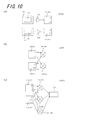
例えば、図10(a)に示すような、上述の実施形態に係るセンサ装置に対する変形例を採用してもよい。 For example, you may employ | adopt the modification with respect to the sensor apparatus which concerns on the above-mentioned embodiment as shown to Fig.10 (a).
上述の実施形態に係るセンサ装置100A、100Bでは、検出素子110およびリファレンス素子120からの信号を直接用いた例について説明した。これに対して、図10(a)に示すセンサ装置100E1のように、検出素子110と第1分岐部131との間およびリファレンス素子120と第2分岐部132との間のそれぞれにローノイズアンプ133(第1ローノイズアンプ133a、第2ローノイズアンプ133b)を配置してもよい。これによれば、次のような場合においても、高い検出精度を得ることができる。
In the
一般にSAWセンサでは、感度が高いと振幅特性の変化も大きくなる。そのため、保護膜4の厚みなどを調整して感度が高くなるような設計とすると、ロスも大きくなり正確な測定ができないおそれがある。しかし、このようにローノイズアンプ133を介在させることで、信号を増幅させて高い検出精度を得ることができる。一方で、計算部140へ入力される信号が小さいと、ノイズが多くなり検出精度が低くなるおそれがあるが、計算部140への入力経路にローノイズアンプ133を介在させることで、信号を増幅させて高い検出精度を得ることができる。ローノイズアンプ133は、計算部140への入力経路のうち各素子110、120に近い側に設けることが好ましい。
In general, in the SAW sensor, when the sensitivity is high, the change in the amplitude characteristic becomes large. For this reason, if the design is such that the thickness of the
また、検出素子110およびリファレンス素子120に入力する信号を大きくすると、互いの入力信号同士が、あるいはこれらの入力信号と他の信号とがクロストークなどによって互いに悪影響を及ぼすおそれがある。これに対して、センサ装置100E1のように検出素子110およびリファレンス素子120からの出力経路にローノイズアンプ133を介在させることで、入力する信号を大きくすることなく、上述のようなクロストークを抑制して高い検出精度を得ることができる。さらに、検出素子110およびリファレンス素子120に入力する信号を大きくすると、互いの入力信号同士が、あるいはこれらの入力信号と他の信号とが電磁波として外部に漏洩するおそれがある。これに対しても、センサ装置100E1のように検出素子110およびリファレンス素子120からの出力経路にローノイズアンプ133を介在させることで、入力する信号を大きくすることなく、上述のような電磁波の外部への漏洩を抑制して高い検出精度を得ることができる。
Further, when the signals input to the
また、図10(b)に示すような、上述の実施形態に係るセンサ装置に対する変形例を採用してもよい。 Moreover, you may employ | adopt the modification with respect to the sensor apparatus which concerns on the above-mentioned embodiment as shown in FIG.10 (b).
上述の実施形態に係るセンサ装置100B〜100Dでは、図2〜図4に示すように、第2分岐部132において、第3分岐信号を第1分岐信号と同じ位相とし、第4分岐信号を第1分岐信号から位相を90°ずらしている。第1〜第4分岐信号の位相の設定はこれに限られるものではなく、第1検出電圧と第2検出電圧とが±180°を除く位相差を有するように設定すればよい。図10(b)に示すセンサ装置100E2のように、例えば、第1分岐信号と第2分岐信号とを同じ位相とし、第3分岐信号を第1分岐信号に対して−45°位相をずらすとともに第4分岐信号を第1分岐信号に対して+45°位相をずらすようにしてもよい。この場合においても、上述の実施形態に係るセンサ装置100B〜100Dと同様の効果を奏することができる。
In the
また、図10(c)に示すような、上述の実施形態に係るセンサ装置に対する変形例を採用してもよい。 Moreover, you may employ | adopt the modification with respect to the sensor apparatus which concerns on the above-mentioned embodiment as shown in FIG.10 (c).
上述の実施形態に係るセンサ装置100B〜100Dでは、図2〜図4に示すように、第1分岐部131および第2分岐部132はそれぞれ2つの信号に分岐するものである。これに代えて、第1分岐部131および第2分岐部132がそれぞれ3つあるいはそれ以上の信号に分岐するように設定してもよい。図10(c)に示すセンサ装置100E3のように、例えば、第1分岐部131および第2分岐部132をそれぞれ3つの信号A、B、B’、B”に分岐する場合は、得られる信号のうち2つずつを用いてヘテロダイン方式によって互いに異なる位相差を有する3つの検出電圧を得ることで、上記センサ装置と同様の効果を奏することが可能となる。しかもこの場合には、3つの検出電圧のそれぞれにおいて傾きの小さい領域が広い場合、言い換えればそれぞれの検出電圧を感度よく計測できる領域が狭い場合であっても、3つの検出電圧からより感度が高い領域を有する検出電圧を選択するように設定することができるため、感度の低下をより効果的に抑制することが可能となる。
In
また、上述の実施形態に係るセンサ装置100は、本発明の技術的思想の範囲内において、互いの構成を適宜組み合わせることよって異なる形態のセンサ装置とすることができるのは言うまでもない。例えば、第1実施形態のセンサ装置100Aの一の構成と、第2実施形態のセンサ装置100Bの他の構成とを組み合わせてもよい。
Further, it goes without saying that the
1・・・圧電基板
2・・・板状体
3・・・カバー
4・・・保護膜
5a・・・検出第1IDT電極
5b・・・リファレンス第1IDT電極
6a・・・検出第2IDT電極
6b・・・リファレンス第2IDT電極
7a、7b・・・金属膜
8・・・配線
9・・・パッド
11a、11b・・・第1振動空間
12a、12b・・・第2振動空間
20・・・空間
31・・・基準電位線
100、100A、100B、100C、100D、100E1、100E2、100E3・・・センサ装置
105・・・素子分岐部
110・・・検出素子
111・・・検出部
115・・・第1接続配線
120・・・リファレンス素子
121・・・リファレンス部
125・・・第2接続配線
130・・・分岐部
131・・・第1分岐部
132・・・第2分岐部
133・・・ローノイズアンプ
135a、135b、135c、135d・・・素子側スイッチ
136a、136b・・・分岐部側スイッチ
140・・・計算部
141・・・第1計算部
142・・・第2計算部
150・・・計測部
160・・・選択部
170・・・検出量算出部
SG・・・信号発生器
SG1・・・第1信号発生器
SG2・・・第2信号発生器
f1・・・第1周波数の信号
f2・・・第2周波数の信号
A、B、B’、B”・・・第1〜第6分岐信号DESCRIPTION OF
Claims (28)
前記第1周波数の信号および前記第2周波数の信号のうち少なくとも一方を発生する第2信号発生器と、
前記第1信号発生器および前記第2信号発生器のそれぞれに接続可能な計算部と、を備え、
前記計算部は、
前記第1信号発生器に前記計算部を接続した状態で、前記第1信号発生器から前記第1周波数の信号を発生して得られた第1基準信号と、前記第2信号発生器に前記計算部を接続した状態で、前記第2信号発生器から前記第2周波数の信号を発生することによって得られた第2基準信号とから基準位相差を得るとともに、前記基準位相差に対応する基準電圧を算出する、センサ装置。 A first signal generator for generating at least one of a first frequency signal and a second frequency signal different from the first frequency;
A second signal generator for generating at least one of the first frequency signal and the second frequency signal;
A calculation unit connectable to each of the first signal generator and the second signal generator,
The calculator is
With the calculation unit connected to the first signal generator, a first reference signal obtained by generating a signal of the first frequency from the first signal generator, and the second signal generator to the second signal generator A reference phase difference is obtained from a second reference signal obtained by generating a signal of the second frequency from the second signal generator in a state where the calculation unit is connected, and a reference corresponding to the reference phase difference A sensor device for calculating a voltage.
前記第2信号発生器および前記計算部に接続可能で、リファレンス部を有するリファレンス素子と、
前記第1信号発生器および前記計算部に接続可能な第1接続配線と、
前記第2信号発生器および前記計算部に接続可能な第2接続配線と、をさらに備え、
前記第1信号発生器は、前記第1接続配線および前記検出素子のいずれか一方に選択的に接続し、
前記第2信号発生器は、前記第2接続配線および前記リファレンス素子のいずれか一方に選択的に接続するように構成される、請求項1または2に記載のセンサ装置。 A detection element that can be connected to the first signal generator and the calculation unit and has a detection unit for detecting a specimen;
A reference element connectable to the second signal generator and the calculation unit and having a reference unit;
A first connection wiring connectable to the first signal generator and the calculation unit;
A second connection wiring connectable to the second signal generator and the calculation unit;
The first signal generator is selectively connected to either the first connection wiring or the detection element;
The sensor device according to claim 1, wherein the second signal generator is configured to be selectively connected to any one of the second connection wiring and the reference element.
前記第1信号発生器、前記検出素子および前記計算部を接続した状態で、前記第1信号発生器から前記第1周波数の信号を発生して得られた第1検出信号と、前記第2信号発生器、前記リファレンス素子および前記計算部を接続した状態で、前記第2信号発生器から前記第1周波数の信号を発生することによって得られた第1リファレンス信号とから検出電圧を算出する、請求項3に記載のセンサ装置。 The calculator is
A first detection signal obtained by generating a signal of the first frequency from the first signal generator in a state where the first signal generator, the detection element, and the calculation unit are connected, and the second signal A detection voltage is calculated from a first reference signal obtained by generating a signal of the first frequency from the second signal generator in a state where the generator, the reference element, and the calculation unit are connected. Item 4. The sensor device according to Item 3.
前記第2信号発生器は、前記第3周波数の信号を発生することが可能であり、
前記計算部は、
前記第1信号発生器、前記検出素子および前記計算部を接続した状態で、前記第1信号発生器から前記第3周波数の信号を発生して得られた第1検出信号と、前記第2信号発生器、前記リファレンス素子および前記計算部を接続した状態で、前記第2信号発生器から前記第3周波数の信号を発生することによって得られた第1リファレンス信号とから検出電圧を算出する、請求項3に記載のセンサ装置。 The first signal generator is capable of generating a signal having a third frequency different from the first frequency and the second frequency;
The second signal generator is capable of generating a signal of the third frequency;
The calculator is
A first detection signal obtained by generating a signal of the third frequency from the first signal generator in a state in which the first signal generator, the detection element and the calculation unit are connected; and the second signal. A detection voltage is calculated from a first reference signal obtained by generating a signal of the third frequency from the second signal generator in a state where the generator, the reference element, and the calculation unit are connected. Item 4. The sensor device according to Item 3.
前記計算部は、
前記第1信号発生器および前記第2信号発生器のうちいずれか一方の信号発生器、前記素子分岐部および前記計算部を接続した状態で、前記一方の信号発生器から信号を発生し、発生した信号を前記素子分岐部で分岐することによって得られた第1検出信号および第1リファレンス信号から検出電圧を算出する、請求項3に記載のセンサ装置。 An element branching section connectable to the detection element and the reference element,
The calculator is
Generates a signal from one of the first signal generator and the second signal generator in a state where one of the signal generators, the element branching unit, and the calculating unit are connected to generate The sensor device according to claim 3, wherein a detection voltage is calculated from a first detection signal and a first reference signal obtained by branching the processed signal at the element branching unit.
前記計測部は、前記基準電圧を参照して得られた前記検出電圧に対応する複数の位相候補値のうちの1つである検出位相差を選定する、請求項4〜6のいずれか1つに記載のセンサ装置。 A measuring unit connected to the calculating unit;
The said measurement part selects the detection phase difference which is one of the several phase candidate values corresponding to the said detection voltage obtained with reference to the said reference voltage, Any one of Claims 4-6 The sensor device according to 1.
前記第1周波数の信号および前記第2周波数の信号のうち少なくとも一方を発生する第2信号発生器と、
前記第1信号発生器に接続可能であり、前記第1信号発生器から得られた第1基準信号を第1分岐信号および第2分岐信号に分岐する、第1分岐部と、
前記第2信号発生器に接続可能であり、前記第2信号発生器から得られた第2基準信号を第3分岐信号および第4分岐信号に分岐する、第2分岐部と、
前記第1信号発生器および前記第1分岐部に接続した状態で、前記第1信号発生器から前記第1周波数の信号を発生して得られた前記第1基準信号に基づく前記第1分岐信号、ならびに前記第2信号発生器および前記第2分岐部に接続した状態で、前記第2信号発生器から前記第2周波数の信号を発生して得られた前記第2基準信号に基づく前記第3分岐信号から第1基準位相差を得るとともに、前記第1基準位相差に対応する第1基準電圧を算出する、第1計算部と、
前記第1信号発生器および前記第1分岐部に接続した状態で、前記第1信号発生器から前記第1周波数の信号を発生して得られた前記第1基準信号に基づく前記第2分岐信号、ならびに前記第2信号発生器および前記第2分岐部に接続した状態で、前記第2信号発生器から前記第2周波数の信号を発生して得られた前記第2基準信号に基づく前記第4分岐信号から第2基準位相差を得るとともに、前記第2基準位相差に対応する第2基準電圧を算出する、第2計算部と、を備えるセンサ装置。 A first signal generator for generating at least one of a first frequency signal and a second frequency signal different from the first frequency;
A second signal generator for generating at least one of the first frequency signal and the second frequency signal;
A first branching unit, connectable to the first signal generator, for branching a first reference signal obtained from the first signal generator into a first branch signal and a second branch signal;
A second branching unit, connectable to the second signal generator, for branching the second reference signal obtained from the second signal generator into a third branching signal and a fourth branching signal;
The first branch signal based on the first reference signal obtained by generating a signal of the first frequency from the first signal generator in a state connected to the first signal generator and the first branch unit. And the third signal based on the second reference signal obtained by generating the signal of the second frequency from the second signal generator in a state connected to the second signal generator and the second branching unit. A first calculation unit that obtains a first reference phase difference from the branch signal and calculates a first reference voltage corresponding to the first reference phase difference;
The second branch signal based on the first reference signal obtained by generating a signal of the first frequency from the first signal generator in a state connected to the first signal generator and the first branch unit. And the fourth signal based on the second reference signal obtained by generating a signal of the second frequency from the second signal generator in a state of being connected to the second signal generator and the second branching unit. A sensor device comprising: a second calculation unit that obtains a second reference phase difference from the branch signal and calculates a second reference voltage corresponding to the second reference phase difference.
前記第2計算部は、前記第2分岐信号と前記第4分岐信号とからヘテロダイン方式によって前記第2基準電圧を算出する、請求項9に記載のセンサ装置。 The first calculation unit calculates the first reference voltage from the first branch signal and the third branch signal by a heterodyne method,
The sensor device according to claim 9, wherein the second calculation unit calculates the second reference voltage from the second branch signal and the fourth branch signal by a heterodyne method.
前記第2信号発生器および前記第2分岐部に接続可能で、リファレンス部を有するリファレンス素子と、
前記第1信号発生器および前記第1分岐部に接続可能な第1接続配線と、
前記第2信号発生器および前記第2分岐部に接続可能な第2接続配線と、をさらに備え、
前記第1信号発生器は、前記第1接続配線および前記検出素子のいずれか一方に選択的に接続し、
前記第2信号発生器は、前記第2接続配線および前記リファレンス素子のいずれか一方に選択的に接続するように構成される、請求項10に記載のセンサ装置。 A detection element that can be connected to the first signal generator and the first branching unit and has a detection unit for detecting a specimen;
A reference element connectable to the second signal generator and the second branching unit and having a reference unit;
A first connection wiring connectable to the first signal generator and the first branch part;
A second connection wiring connectable to the second signal generator and the second branch part; and
The first signal generator is selectively connected to either the first connection wiring or the detection element;
The sensor device according to claim 10, wherein the second signal generator is configured to be selectively connected to any one of the second connection wiring and the reference element.
前記第2分岐部は、前記リファレンス素子にさらに接続可能であり、前記リファレンス素子から得られたリファレンス信号を前記第3分岐信号および前記第4分岐信号に分岐し、
前記第1計算部は、
前記第1信号発生器、前記検出素子、前記第1分岐部および前記第1計算部を接続した状態で、前記第1信号発生器から前記第1周波数の信号を発生して得られた第1分岐検出信号に基づく前記第1分岐信号、ならびに前記第2信号発生器、前記リファレンス素子、前記第2分岐部および前記第2計算部を接続した状態で、前記第2信号発生器から前記第1周波数の信号を発生して得られた第1分岐リファレンス信号に基づく前記第3分岐信号から第1検出電圧を算出し、
前記第2計算部は、
前記第1信号発生器、前記検出素子、前記第1分岐部および前記第1計算部を接続した状態で、前記第1信号発生器から前記第1周波数の信号を発生して得られた第2分岐検出信号に基づく前記第2分岐信号、ならびに前記第2信号発生器、前記リファレンス素子、前記第2分岐部および前記第2計算部を接続した状態で、前記第2信号発生器から前記第1周波数の信号を発生して得られた第2分岐リファレンス信号に基づく前記第4分岐信号から第2検出電圧を算出する、請求項11に記載のセンサ装置。 The first branch unit is further connectable to the detection element, branches a detection signal obtained from the detection element into the first branch signal and the second branch signal,
The second branch unit is further connectable to the reference element, branches a reference signal obtained from the reference element into the third branch signal and the fourth branch signal,
The first calculator is
First obtained by generating a signal of the first frequency from the first signal generator in a state where the first signal generator, the detection element, the first branching unit, and the first calculating unit are connected. The first branch signal based on the branch detection signal, and the second signal generator, the reference element, the second branch unit, and the second calculation unit are connected to the first signal from the second signal generator. Calculating a first detection voltage from the third branch signal based on a first branch reference signal obtained by generating a signal of frequency;
The second calculator is
A second obtained by generating a signal of the first frequency from the first signal generator in a state where the first signal generator, the detection element, the first branching unit, and the first calculating unit are connected. The second branch signal based on the branch detection signal, the second signal generator, the reference element, the second branch section, and the second calculation section are connected to the first branch signal from the second signal generator. The sensor device according to claim 11, wherein a second detection voltage is calculated from the fourth branch signal based on a second branch reference signal obtained by generating a frequency signal.
前記第2計算部は、前記第2分岐信号と前記第4分岐信号とからヘテロダイン方式によって前記第2検出電圧を算出する、請求項12に記載のセンサ装置。The sensor device according to claim 12, wherein the second calculation unit calculates the second detection voltage from the second branch signal and the fourth branch signal by a heterodyne method.
前記計測部は、前記第1計算部および前記第2計算部に接続され、前記第1基準電圧を参照して得られた前記第1検出電圧に対応する複数の第1位相候補値、および前記第2基準電圧を参照して得られた前記第2検出電圧に対応する複数の第2位相候補値、のうち1つの位相候補値である検出位相差を選定する、請求項12または13に記載のセンサ装置。 A measurement unit connected to the first calculation unit and the second calculation unit;
The measurement unit is connected to the first calculation unit and the second calculation unit, and a plurality of first phase candidate values corresponding to the first detection voltage obtained by referring to the first reference voltage, and a plurality of second candidate phase value corresponding to the second detection voltage obtained by reference to a second reference voltage, selects the detected phase difference which is one candidate phase value among, according to claim 12 or 13 Sensor device.
前記第1出力部および前記第2出力部のそれぞれに接続可能な計算部と、を備え、
前記計算部は、
前記第1出力部に前記計算部を接続した状態で、前記第1出力部から前記第1周波数の信号を出力して得られた第1基準信号と、前記第2出力部に前記計算部を接続した状態で、前記第2出力部から前記第2周波数の信号を出力することによって得られた第2基準信号とから基準位相差を得るとともに、前記基準位相差に対応する基準電圧を算出する、センサ装置。 A signal generator for generating a first frequency signal and a second frequency signal different from the first frequency, wherein the first frequency signal outputs at least one of the first frequency signal and the second frequency signal. A signal generator including an output unit, and a second output unit that outputs at least one of the first frequency signal and the second frequency signal;
A calculation unit connectable to each of the first output unit and the second output unit,
The calculator is
With the calculation unit connected to the first output unit, the first reference signal obtained by outputting the signal of the first frequency from the first output unit, and the calculation unit to the second output unit In a connected state, a reference phase difference is obtained from the second reference signal obtained by outputting the signal of the second frequency from the second output unit, and a reference voltage corresponding to the reference phase difference is calculated. , Sensor device.
前記第1出力部に接続可能であり、前記第1出力部から得られた第1基準信号を第1分岐信号および第2分岐信号に分岐する、第1分岐部と、
前記第2出力部に接続可能であり、前記第2出力部から得られた第2基準信号を第3分岐信号および第4分岐信号に分岐する、第2分岐部と、
前記第1出力部および前記第1分岐部に接続した状態で、前記第1出力部から前記第1周波数の信号を出力して得られた前記第1基準信号に基づく前記第1分岐信号、ならびに前記第2出力部および前記第2分岐部に接続した状態で、前記第2出力部から前記第2周波数の信号を出力して得られた前記第2基準信号に基づく前記第3分岐信号から第1基準位相差を得るとともに、前記第1基準位相差に対応する第1基準電圧を算出する、第1計算部と、
前記第1出力部および前記第1分岐部に接続した状態で、前記第1出力部から前記第1周波数の信号を出力して得られた前記第1基準信号に基づく前記第2分岐信号、ならびに前記第2出力部および前記第2分岐部に接続した状態で、前記第2出力部から前記第2周波数の信号を出力して得られた前記第2基準信号に基づく前記第4分岐信号から第2基準位相差を得るとともに、前記第2基準位相差に対応する第2基準電圧を算出する、第2計算部と、を備えるセンサ装置。 A signal generator for generating a first frequency signal and a second frequency signal different from the first frequency, wherein the first frequency signal outputs at least one of the first frequency signal and the second frequency signal. A signal generator comprising: an output unit; and a second output unit that outputs at least one of the first frequency signal and the second frequency signal;
A first branching unit, connectable to the first output unit, for branching a first reference signal obtained from the first output unit into a first branch signal and a second branch signal;
A second branching unit, connectable to the second output unit, for branching the second reference signal obtained from the second output unit into a third branch signal and a fourth branch signal;
The first branch signal based on the first reference signal obtained by outputting the signal of the first frequency from the first output unit in a state connected to the first output unit and the first branch unit, and From the third branch signal based on the second reference signal obtained by outputting the signal of the second frequency from the second output unit in a state connected to the second output unit and the second branch unit. A first calculator for obtaining a first reference phase difference and calculating a first reference voltage corresponding to the first reference phase difference;
The second branch signal based on the first reference signal obtained by outputting the signal of the first frequency from the first output unit in a state connected to the first output unit and the first branch unit; and From the fourth branch signal based on the second reference signal obtained by outputting the signal of the second frequency from the second output unit in a state connected to the second output unit and the second branch unit. A sensor device comprising: a second calculator that obtains a second reference phase difference and calculates a second reference voltage corresponding to the second reference phase difference.
計算部が、前記信号発生器が出力した第1周波数の信号から得られる第1基準信号、および前記信号発生器が前記第1周波数の信号と同時に出力した第2周波数の信号から得られる第2基準信号とから基準位相差を得るとともに、前記第1基準信号と前記第2基準信号とから前記基準位相差に対応する基準電圧を算出する算出工程と、を含むセンシング方法。 A signal output step of generating and outputting a signal having a first frequency and a signal having a second frequency different from the first frequency;
A calculation unit obtains a first reference signal obtained from the first frequency signal output from the signal generator, and a second frequency obtained from the second frequency signal output from the signal generator simultaneously with the first frequency signal. A sensing method comprising: obtaining a reference phase difference from a reference signal, and calculating a reference voltage corresponding to the reference phase difference from the first reference signal and the second reference signal.
Applications Claiming Priority (5)
| Application Number | Priority Date | Filing Date | Title |
|---|---|---|---|
| JP2014175768 | 2014-08-29 | ||
| JP2014175768 | 2014-08-29 | ||
| JP2015130676 | 2015-06-30 | ||
| JP2015130676 | 2015-06-30 | ||
| PCT/JP2015/074809 WO2016032008A1 (en) | 2014-08-29 | 2015-08-31 | Sensor device and sensing method |
Related Child Applications (1)
| Application Number | Title | Priority Date | Filing Date |
|---|---|---|---|
| JP2018065904A Division JP2018138920A (en) | 2014-08-29 | 2018-03-29 | Sensor device and sensing method |
Publications (2)
| Publication Number | Publication Date |
|---|---|
| JPWO2016032008A1 JPWO2016032008A1 (en) | 2017-04-27 |
| JP6317455B2 true JP6317455B2 (en) | 2018-04-25 |
Family
ID=55399888
Family Applications (2)
| Application Number | Title | Priority Date | Filing Date |
|---|---|---|---|
| JP2016545666A Active JP6317455B2 (en) | 2014-08-29 | 2015-08-31 | Sensor device and sensing method |
| JP2018065904A Pending JP2018138920A (en) | 2014-08-29 | 2018-03-29 | Sensor device and sensing method |
Family Applications After (1)
| Application Number | Title | Priority Date | Filing Date |
|---|---|---|---|
| JP2018065904A Pending JP2018138920A (en) | 2014-08-29 | 2018-03-29 | Sensor device and sensing method |
Country Status (5)
| Country | Link |
|---|---|
| US (1) | US10859532B2 (en) |
| EP (1) | EP3187869B1 (en) |
| JP (2) | JP6317455B2 (en) |
| CN (1) | CN106461612B (en) |
| WO (1) | WO2016032008A1 (en) |
Families Citing this family (2)
| Publication number | Priority date | Publication date | Assignee | Title |
|---|---|---|---|---|
| JP6317455B2 (en) | 2014-08-29 | 2018-04-25 | 京セラ株式会社 | Sensor device and sensing method |
| WO2020090944A1 (en) * | 2018-10-30 | 2020-05-07 | 京セラ株式会社 | Measuring device and measuring method |
Family Cites Families (31)
| Publication number | Priority date | Publication date | Assignee | Title |
|---|---|---|---|---|
| US4129566A (en) * | 1978-02-15 | 1978-12-12 | E. R. Squibb & Sons, Inc. | Derivatives of dehydrocyclicimino acids |
| US4516084A (en) * | 1983-02-18 | 1985-05-07 | Rca Corporation | Frequency synthesizer using an arithmetic frequency synthesizer and plural phase locked loops |
| JPH0450543Y2 (en) * | 1985-08-30 | 1992-11-27 | ||
| JPS63252080A (en) * | 1987-04-08 | 1988-10-19 | Pioneer Electronic Corp | Video signal output device |
| US5306644A (en) | 1988-09-29 | 1994-04-26 | Hewlett-Packard Company | Mass sensor method for measuring analytes in a sample |
| US4951009A (en) * | 1989-08-11 | 1990-08-21 | Applied Materials, Inc. | Tuning method and control system for automatic matching network |
| US5763283A (en) * | 1994-10-12 | 1998-06-09 | Sandia Corporation | Method and apparatus for phase for and amplitude detection |
| US5786733A (en) * | 1995-12-04 | 1998-07-28 | Nec Corporation | Phase-locked oscillating circuit with a frequency fluctuation detecting circuit |
| US7741753B2 (en) * | 1996-08-05 | 2010-06-22 | Puskas William L | Megasonic apparatus, circuitry, signals and methods for cleaning and/or processing |
| JPH1183757A (en) * | 1997-09-08 | 1999-03-26 | Toshiba Fa Syst Eng Kk | Microwave densitometer |
| US6311046B1 (en) * | 1998-04-02 | 2001-10-30 | Ericsson Inc. | Linear amplification systems and methods using more than two constant length vectors |
| DE10114779A1 (en) * | 2001-03-26 | 2002-10-24 | Infineon Technologies Ag | Sending and receiving unit |
| ATE356483T1 (en) * | 2003-08-29 | 2007-03-15 | Koninkl Philips Electronics Nv | PHASE DETECTOR |
| JP4715236B2 (en) * | 2005-03-01 | 2011-07-06 | 株式会社デンソー | Ultrasonic sensor device |
| JP2007145108A (en) * | 2005-11-25 | 2007-06-14 | Ihi Aerospace Co Ltd | Turning control method for traveling vehicle |
| KR100714579B1 (en) * | 2005-11-25 | 2007-05-07 | 삼성전기주식회사 | Phase Frequency Detector with Improved Noise Characteristics |
| WO2007145108A1 (en) | 2006-06-16 | 2007-12-21 | Murata Manufacturing Co., Ltd. | Sensor for detecting substance in liquid |
| WO2009015086A2 (en) * | 2007-07-20 | 2009-01-29 | Blue Danube Labs Inc | Method and system for multi-point signal generation with phase synchronized local carriers |
| JP2009029209A (en) * | 2007-07-25 | 2009-02-12 | Texas Instr Japan Ltd | Tire monitoring device and tire failure detection device |
| US7994800B2 (en) | 2008-03-25 | 2011-08-09 | General Electric Company | Systems and methods for online phase calibration |
| US8716896B2 (en) * | 2008-12-12 | 2014-05-06 | Caterpillar Inc. | Genset control system implementing engine synchronization |
| US9378930B2 (en) * | 2009-03-05 | 2016-06-28 | Applied Materials, Inc. | Inductively coupled plasma reactor having RF phase control and methods of use thereof |
| ES2333088B2 (en) * | 2009-06-23 | 2011-02-07 | Universidad Politecnica De Valencia | METHOD AND DEVICE OF NANOGRAVIMETRY IN FLUID MEDIA BASED ON PIEZOELECTRIC RESONATORS. |
| JP5601205B2 (en) * | 2011-01-07 | 2014-10-08 | 富士通株式会社 | Optical receiver and optical communication system |
| CN103354917B (en) * | 2011-02-25 | 2016-08-10 | 3M创新有限公司 | Front illuminated reflection display device |
| WO2013115175A1 (en) * | 2012-01-30 | 2013-08-08 | 京セラ株式会社 | Specimen sensor and specimen-sensing method |
| JP5917973B2 (en) * | 2012-03-28 | 2016-05-18 | 京セラ株式会社 | SAW sensor and SAW sensor device |
| GB2506939B (en) * | 2012-10-15 | 2017-04-05 | Alphasonics (Ultrasonic Cleaning Systems) Ltd | Improvements in and relating to ultrasonic cleaning |
| JP6042774B2 (en) * | 2013-05-30 | 2016-12-14 | 京セラ株式会社 | Sample sensor and sample sensing method |
| JP6375756B2 (en) * | 2014-07-28 | 2018-08-22 | 大日本印刷株式会社 | SEALING MATERIAL SHEET FOR SOLAR CELL MODULE AND METHOD FOR PRODUCING THE SAME |
| JP6317455B2 (en) | 2014-08-29 | 2018-04-25 | 京セラ株式会社 | Sensor device and sensing method |
-
2015
- 2015-08-31 JP JP2016545666A patent/JP6317455B2/en active Active
- 2015-08-31 CN CN201580027308.8A patent/CN106461612B/en active Active
- 2015-08-31 WO PCT/JP2015/074809 patent/WO2016032008A1/en not_active Ceased
- 2015-08-31 US US15/324,242 patent/US10859532B2/en active Active
- 2015-08-31 EP EP15836465.3A patent/EP3187869B1/en active Active
-
2018
- 2018-03-29 JP JP2018065904A patent/JP2018138920A/en active Pending
Also Published As
| Publication number | Publication date |
|---|---|
| WO2016032008A1 (en) | 2016-03-03 |
| JPWO2016032008A1 (en) | 2017-04-27 |
| US10859532B2 (en) | 2020-12-08 |
| CN106461612A (en) | 2017-02-22 |
| EP3187869A1 (en) | 2017-07-05 |
| JP2018138920A (en) | 2018-09-06 |
| CN106461612B (en) | 2020-10-16 |
| US20170205375A1 (en) | 2017-07-20 |
| EP3187869A4 (en) | 2018-03-28 |
| EP3187869B1 (en) | 2023-03-08 |
Similar Documents
| Publication | Publication Date | Title |
|---|---|---|
| JP6568126B2 (en) | Sample sensor and sample sensing method | |
| US10241082B2 (en) | Analyte sensor and analyte sensing method | |
| JP4900387B2 (en) | Submerged substance detection sensor | |
| JP6317455B2 (en) | Sensor device and sensing method | |
| JP6466533B2 (en) | Sample sensor and sample sensing method | |
| JP6391653B2 (en) | Sample sensor and sample sensing method | |
| JP6193956B2 (en) | Sample sensor and sample sensing method | |
| JP5837233B2 (en) | Sample sensor and sample sensing method | |
| JP2017020937A (en) | Sensing system | |
| JP2014190815A (en) | Elastic surface wave device and physical quantity detector using the same | |
| JP2017215344A5 (en) | ||
| CN104713607A (en) | Method for determination of the time of flight of the signals in the signal paths of a coriolis flow meter |
Legal Events
| Date | Code | Title | Description |
|---|---|---|---|
| A131 | Notification of reasons for refusal |
Free format text: JAPANESE INTERMEDIATE CODE: A131 Effective date: 20170725 |
|
| A521 | Request for written amendment filed |
Free format text: JAPANESE INTERMEDIATE CODE: A523 Effective date: 20170925 |
|
| TRDD | Decision of grant or rejection written | ||
| A01 | Written decision to grant a patent or to grant a registration (utility model) |
Free format text: JAPANESE INTERMEDIATE CODE: A01 Effective date: 20180227 |
|
| A61 | First payment of annual fees (during grant procedure) |
Free format text: JAPANESE INTERMEDIATE CODE: A61 Effective date: 20180329 |
|
| R150 | Certificate of patent or registration of utility model |
Ref document number: 6317455 Country of ref document: JP Free format text: JAPANESE INTERMEDIATE CODE: R150 |