JP6316957B2 - System and method for extending the power performance of a wireless charger - Google Patents
System and method for extending the power performance of a wireless charger Download PDFInfo
- Publication number
- JP6316957B2 JP6316957B2 JP2016529792A JP2016529792A JP6316957B2 JP 6316957 B2 JP6316957 B2 JP 6316957B2 JP 2016529792 A JP2016529792 A JP 2016529792A JP 2016529792 A JP2016529792 A JP 2016529792A JP 6316957 B2 JP6316957 B2 JP 6316957B2
- Authority
- JP
- Japan
- Prior art keywords
- voltage
- input voltage
- circuit
- level threshold
- converter circuit
- Prior art date
- Legal status (The legal status is an assumption and is not a legal conclusion. Google has not performed a legal analysis and makes no representation as to the accuracy of the status listed.)
- Active
Links
Images


Classifications
-
- H—ELECTRICITY
- H02—GENERATION; CONVERSION OR DISTRIBUTION OF ELECTRIC POWER
- H02J—CIRCUIT ARRANGEMENTS OR SYSTEMS FOR SUPPLYING OR DISTRIBUTING ELECTRIC POWER; SYSTEMS FOR STORING ELECTRIC ENERGY
- H02J50/00—Circuit arrangements or systems for wireless supply or distribution of electric power
- H02J50/10—Circuit arrangements or systems for wireless supply or distribution of electric power using inductive coupling
- H02J50/12—Circuit arrangements or systems for wireless supply or distribution of electric power using inductive coupling of the resonant type
-
- H—ELECTRICITY
- H02—GENERATION; CONVERSION OR DISTRIBUTION OF ELECTRIC POWER
- H02J—CIRCUIT ARRANGEMENTS OR SYSTEMS FOR SUPPLYING OR DISTRIBUTING ELECTRIC POWER; SYSTEMS FOR STORING ELECTRIC ENERGY
- H02J7/00—Circuit arrangements for charging or depolarising batteries or for supplying loads from batteries
- H02J7/34—Parallel operation in networks using both storage and other dc sources, e.g. providing buffering
-
- H—ELECTRICITY
- H02—GENERATION; CONVERSION OR DISTRIBUTION OF ELECTRIC POWER
- H02J—CIRCUIT ARRANGEMENTS OR SYSTEMS FOR SUPPLYING OR DISTRIBUTING ELECTRIC POWER; SYSTEMS FOR STORING ELECTRIC ENERGY
- H02J50/00—Circuit arrangements or systems for wireless supply or distribution of electric power
- H02J50/60—Circuit arrangements or systems for wireless supply or distribution of electric power responsive to the presence of foreign objects, e.g. detection of living beings
-
- H—ELECTRICITY
- H02—GENERATION; CONVERSION OR DISTRIBUTION OF ELECTRIC POWER
- H02J—CIRCUIT ARRANGEMENTS OR SYSTEMS FOR SUPPLYING OR DISTRIBUTING ELECTRIC POWER; SYSTEMS FOR STORING ELECTRIC ENERGY
- H02J50/00—Circuit arrangements or systems for wireless supply or distribution of electric power
- H02J50/90—Circuit arrangements or systems for wireless supply or distribution of electric power involving detection or optimisation of position, e.g. alignment
-
- H—ELECTRICITY
- H02—GENERATION; CONVERSION OR DISTRIBUTION OF ELECTRIC POWER
- H02J—CIRCUIT ARRANGEMENTS OR SYSTEMS FOR SUPPLYING OR DISTRIBUTING ELECTRIC POWER; SYSTEMS FOR STORING ELECTRIC ENERGY
- H02J7/00—Circuit arrangements for charging or depolarising batteries or for supplying loads from batteries
Description
本出願は、一般に、ワイヤレス電力に関する。より詳細には、本開示は、ワイヤレス電力伝達システムにおける送信機および受信機を対象とする。 The present application relates generally to wireless power. More particularly, the present disclosure is directed to transmitters and receivers in wireless power transfer systems.
ますます多くの様々な電子デバイスが、充電式バッテリーを介して給電されている。そのようなデバイスには、モバイルフォン、携帯型音楽プレーヤ、ラップトップコンピュータ、タブレットコンピュータ、コンピュータ周辺デバイス、通信デバイス(たとえば、ブルートゥースデバイス)、デジタルカメラ、補聴器などが含まれる。バッテリー技術は向上してきたが、バッテリー電源式電子デバイスは、より多くの電力量をますます必要とし消費するので、頻繁に充電する必要がある。充電式デバイスは、多くの場合に、電源に物理的に接続されるケーブルまたは他の同様のコネクタを通して有線接続によって充電される。ケーブルおよび同様のコネクタは、不便であるか、または扱いにくく、他の欠点を有することが時々ある。充電式電子デバイスを充電するか、または電子デバイスに電力を提供するのに用いられることになる電力を自由空間において伝達することができるワイヤレス充電システムは、有線式の充電解決策の欠点の一部を克服し得る。したがって、電子デバイスに電力を効率的かつ安全に伝達するワイヤレス電力伝達システムおよび方法が望ましい。 An increasing number of different electronic devices are powered via rechargeable batteries. Such devices include mobile phones, portable music players, laptop computers, tablet computers, computer peripheral devices, communication devices (eg, Bluetooth devices), digital cameras, hearing aids, and the like. While battery technology has improved, battery-powered electronic devices require more and more power and therefore need to be charged frequently. Rechargeable devices are often charged by a wired connection through a cable or other similar connector that is physically connected to a power source. Cables and similar connectors are sometimes inconvenient or cumbersome and sometimes have other drawbacks. Wireless charging systems that can transfer power in free space that will be used to charge or provide power to a rechargeable electronic device are some of the shortcomings of wired charging solutions Can be overcome. Accordingly, wireless power transfer systems and methods that efficiently and safely transfer power to electronic devices are desirable.
添付の特許請求の範囲内のシステム、方法、およびデバイスの様々な実装形態は各々、いくつかの態様を有し、そのいずれの態様も単独では、本明細書で説明する望ましい属性に関与することはない。添付の特許請求の範囲を限定することなく、本明細書においていくつかの顕著な特徴について説明する。 Each of the various implementations of systems, methods, and devices within the scope of the appended claims has a number of aspects, each of which alone contributes to the desired attributes described herein. There is no. Without limiting the scope of the appended claims, some salient features are described herein.
本明細書で説明する主題の1つまたは複数の実装形態の詳細について、添付の図面および以下の説明において述べる。他の特徴、態様、および利点は、説明、図面、および特許請求の範囲から明らかになるであろう。以下の図の相対的な寸法は、一定の縮尺で描かれていないことがあることに留意されたい。 The details of one or more implementations of the subject matter described in this specification are set forth in the accompanying drawings and the description below. Other features, aspects, and advantages will be apparent from the description, drawings, and claims. Note that the relative dimensions in the following figures may not be drawn to scale.
特定の実施形態では、充電可能デバイスを充電するためのワイヤレス電力受信機装置が提供される。充電可能デバイスを充電するためのワイヤレス電力受信機装置は、充電可能デバイスを充電するのに十分なレベルで電力をワイヤレス受信するように構成された受信アンテナを含み得る。ワイヤレス電力受信機装置は、変換器回路も含み得る。変換器回路は、受信アンテナに結合され得る。変換器回路は、ワイヤレス受信された電力から導出された入力電圧を受け取るように構成され得る。変換器回路はまた、入力電圧と第1の電圧レベルしきい値との間の関係に基づいて入力電圧に対するある値にスケーリングされた出力電圧を生成するように構成され得る。 In certain embodiments, a wireless power receiver apparatus for charging a rechargeable device is provided. A wireless power receiver apparatus for charging a rechargeable device may include a receive antenna configured to wirelessly receive power at a level sufficient to charge the rechargeable device. The wireless power receiver device may also include a converter circuit. The converter circuit may be coupled to the receive antenna. The converter circuit may be configured to receive an input voltage derived from wirelessly received power. The converter circuit may also be configured to generate an output voltage scaled to a value for the input voltage based on the relationship between the input voltage and the first voltage level threshold.
別の特定の実施形態では、充電可能デバイスを充電するためのワイヤレス電力受信機装置が提供される。充電可能デバイスを充電するためのワイヤレス電力受信機装置は、充電可能デバイスを充電するのに十分なレベルで電力をワイヤレス受信するための手段を含み得る。充電可能デバイスを充電するためのワイヤレス電力受信機装置は、電力をワイヤレス受信するための手段に結合された、ワイヤレス受信された電力から導出された入力電圧を受け取るための手段も含み得る。充電可能デバイスを充電するためのワイヤレス電力受信機装置は、入力電圧と第1の電圧レベルしきい値との間の関係に基づいて入力電圧に対するある値にスケーリングされた、入力電圧を受け取るための手段からの出力電圧を生成するための手段も含み得る。 In another particular embodiment, a wireless power receiver apparatus for charging a rechargeable device is provided. A wireless power receiver apparatus for charging a rechargeable device may include means for wirelessly receiving power at a level sufficient to charge the rechargeable device. The wireless power receiver apparatus for charging the rechargeable device may also include means for receiving an input voltage derived from the wirelessly received power coupled to the means for wirelessly receiving the power. A wireless power receiver device for charging a rechargeable device for receiving an input voltage scaled to a value relative to the input voltage based on a relationship between the input voltage and a first voltage level threshold Means for generating an output voltage from the means may also be included.
別の特定の実施形態では、充電可能デバイスを充電するための手段は、受信アンテナにおいて充電可能デバイスを充電するのに十分なレベルで電力をワイヤレス受信するステップを含み得る。本方法は、受信アンテナに結合された変換器回路においてワイヤレス受信された電力から導出された入力電圧を受け取るステップも含み得る。本方法は、入力電圧と第1の電圧レベルしきい値との間の関係に基づいて入力電圧に対するある値にスケーリングされた、変換器回路からの出力電圧を生成するステップも含み得る。 In another particular embodiment, the means for charging the chargeable device may include wirelessly receiving power at a level sufficient to charge the chargeable device at the receiving antenna. The method may also include receiving an input voltage derived from wirelessly received power at a converter circuit coupled to the receive antenna. The method may also include generating an output voltage from the converter circuit that is scaled to a value for the input voltage based on the relationship between the input voltage and the first voltage level threshold.
添付の図面に関して下記に詳細に記載される説明は、例示的な実施形態を説明するためのものであり、実践することができる唯一の実施形態を表すためのものではない。本説明全体にわたって使用される「例示的」という用語は、「例、実例、または例示として機能すること」を意味しており、必ずしも、他の例示的な実施態様よりも好ましい、または有利であると解釈されるべきではない。詳細に記載される説明は、例示的な実施形態の完全な理解をもたらすための具体的な詳細を含んでいる。場合によっては、いくつかのデバイスがブロック図の形式で示されている。 The description set forth in detail below with reference to the accompanying drawings is intended to illustrate exemplary embodiments and not to represent the only embodiments that may be practiced. The term “exemplary” as used throughout this description means “serving as an example, instance, or illustration” and is necessarily preferred or advantageous over other exemplary embodiments. Should not be interpreted. The detailed description includes specific details for a thorough understanding of the exemplary embodiments. In some cases, several devices are shown in block diagram form.
ワイヤレスで電力を伝達することは、物理的な導電体を使用することなく、電場、磁場、電磁場などに関連する任意の形態のエネルギーを送信機から受信機に伝達する(たとえば、電力は、自由空間を通って伝達され得る)ことを指す場合がある。電力伝達を実現するために、ワイヤレス場(たとえば、磁場または電磁場)内に出力された電力は、「受信アンテナ」によって受信され、捕捉され、または結合され得る。本明細書全体にわたって、「結合」されている2つの構成要素は、直接的または間接的な方法を介したそれらの相互作用を指す場合があり、物理的に接続された(たとえば、有線の)結合または物理的に切断された(たとえば、ワイヤレスの)結合をさらに指す場合があることが理解されよう。 Transmitting power wirelessly transfers any form of energy related to electric, magnetic, electromagnetic fields, etc. from a transmitter to a receiver without using physical conductors (e.g., power is free May be transmitted through space). To achieve power transfer, power output in a wireless field (eg, a magnetic or electromagnetic field) can be received, captured, or combined by a “receive antenna”. Throughout this specification, two components that are “coupled” may refer to their interaction via direct or indirect methods and are physically connected (eg, wired). It will be understood that it may further refer to a bond or a physically broken (eg, wireless) bond.
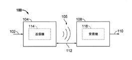
図1は、例示的な実施形態による、例示的なワイヤレス電力伝達システム100の機能ブロック図である。エネルギー伝達を可能にするために、場105を生成するのに、電源(図示せず)から、送信機104に入力電力102を提供することができる。受信機108は、場105に結合し、出力電力110に結合されたデバイス(図示せず)によって蓄積または消費するための出力電力110を生成することができる。送信機104と受信機108の両方は互いに距離112だけ離間される。例示的な一実施形態では、送信機104および受信機108は、相互共振関係に従って構成される。受信機108の共振周波数および送信機104の共振周波数が、ほぼ同じか、または極めて近いとき、送信機104と受信機108との間の伝送損失は最小となる。したがって、大型コイルが極めて近い(たとえば、mm)ことが必要であり得る純粋に誘導性の解決策とは対照的に、より大きい距離にわたる、ワイヤレス電力伝達を可能にすることができる。したがって、共振誘導結合技法は、効率の改善と、様々な距離にわたる様々な誘導コイル構成を用いた電力伝達とを可能にし得る。
FIG. 1 is a functional block diagram of an example wireless
受信機108は、送信機104によって生成されたエネルギー場105内に位置する際に電力を受信し得る。場105は、送信機104によって出力されたエネルギーが受信機108によって捕捉され得る領域に相当する。場合によっては、場105は、以下でさらに説明するように、送信機104の「近接場」に相当し得る。送信機104は、エネルギー伝送を出力するための送信アンテナ114(たとえば、送信コイル)を含み得る。受信機108は、エネルギー伝送からエネルギーを受信するか、または捕捉するための受信アンテナ118(たとえば、受信コイル)をさらに含む。近接場は、送信アンテナ114から電力を最小限に放出する、送信アンテナ114内の電流および電荷から生じる強い反応場(reactive field)が存在する領域に相当し得る。場合によっては、近接場は、送信アンテナ114の約1波長(または1波長の数分の一)内にある領域に相当し得る。送信アンテナ114および受信アンテナ118は、それらに関連付けられる応用形態およびデバイスに応じてサイズを決定される。上述のように、効率的なエネルギー伝達は、電磁波のエネルギーの大部分を遠距離場に伝搬するのではなく、送信アンテナ114の場105のエネルギーの大部分を受信アンテナ118に結合することによって起こり得る。場105内に配置されるとき、送信アンテナ114と受信アンテナ118との間に、「結合モード」を発生させることができる。この結合が起こり得る、送信アンテナ114および受信アンテナ118の周りのエリアは、本明細書では結合モード領域と呼ばれる。
図2は、例示的な実施形態による、図1のワイヤレス電力伝達システム100において使用され得る例示的な構成要素の機能ブロック図である。送信機204は、発振器222、ドライバ回路224、およびフィルタ/整合回路226を含み得る、送信回路206を含むことができる。発振器222は、周波数制御信号223に応答して調整され得る、468.75KHz、6.78MHz、または13.56MHzなどの所望の周波数の信号を生成するように構成され得る。発振器信号は、たとえば送信アンテナ214の共振周波数において送信アンテナ214を駆動するように構成されたドライバ回路224に提供され得る。ドライバ回路224は、発振器222から方形波を受信し、正弦波を出力するように構成されたスイッチング増幅器であり得る。たとえば、ドライバ回路224は、E級増幅器であり得る。フィルタ/整合回路226は、高調波または他の不要な周波数をフィルタ除去し、送信機204のインピーダンスを送信アンテナ214に整合させるために含まれる場合もある。送信アンテナ214を駆動した結果として、送信機204は、電子デバイスを充電または給電するのに十分なレベルで電力をワイヤレスで出力し得る。一例として、提供される電力は、異なる電力要件を有する異なるデバイスを給電または充電するために、たとえば、300ミリワットから5ワット程度であり得る。より高いまたは低い電力レベルも提供できる。
FIG. 2 is a functional block diagram of exemplary components that may be used in the wireless
受信機208は、整合回路232と、図2に示すバッテリー236を充電するかまたは受信機208に結合されたデバイス(図示せず)に給電するために、AC電力入力からDC電力出力を生成するための整流器/スイッチング回路234とを含み得る受信回路210を含むことができる。整合回路232は、受信回路210のインピーダンスを受信アンテナ218に整合させるために含まれ得る。それに加えて、受信機208および送信機204は、別の通信チャネル219(たとえば、ブルートゥース、zigbee、セルラーなど)上で通信し得る。代替的には、受信機208および送信機204は、ワイヤレス場205の特性を使用して帯域内シグナリングを介して通信し得る。
The
以下でより十分に説明するように、最初に選択的に無効にされた関連する負荷(たとえば、バッテリー236)を有し得る受信機208は、送信機204によって送信され受信機208によって受信される電力量がバッテリー236を充電するのに適しているかどうかを判定するように構成され得る。さらに、受信機208は、電力量が適切であると判定すると、負荷(たとえば、バッテリー236)を有効にするように構成され得る。いくつかの実施形態では、受信機208は、バッテリー236の充電なしに、ワイヤレス電力伝達場から受信した電力を直接利用するように構成され得る。たとえば、近接場通信(NFC)または無線周波数識別デバイス(RFID)などの通信デバイスは、ワイヤレス電力伝達場から電力を受け取り、ワイヤレス電力伝達場と相互作用することによって通信し、かつ/または送信機204もしくは他のデバイスと通信するために受信電力を利用するように構成され得る。
As will be described more fully below, a
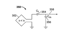
図3は、例示的な実施形態による、送信アンテナまたは受信アンテナ352を含む、図2の送信回路206または受信回路210の一部分の概略図である。図3に示すように、以下で説明するものを含む例示的な実施形態において使用される送信回路または受信回路350は、アンテナ352を含み得る。アンテナ352は、「ループ」アンテナ352と呼ばれるか、または「ループ」アンテナ352として構成される場合もある。また、アンテナ352は、本明細書では、「磁気」アンテナもしくは誘導コイルと呼ばれるか、または「磁気」アンテナもしくは誘導コイルとして構成される場合もある。「アンテナ」という用語は、一般に、別の「アンテナ」への結合からエネルギーをワイヤレスで出力するか、または受信することができる構成要素を指す。アンテナは、電力をワイヤレスで出力するか、または受信するように構成されるタイプのコイルと呼ばれる場合もある。本明細書で使用するアンテナ352は、電力をワイヤレスで出力および/または受信するように構成されるタイプの「電力伝達構成要素」の一例である。アンテナ352は、空芯、またはフェライトコア(図示せず)などの物理的コアを含むように構成され得る。空芯ループアンテナ352により、コアエリア内に他の構成要素を配置することが可能になる。加えて、空芯ループにより、送信アンテナ214(図2)の結合モード領域がより強力であり得る、送信アンテナ214(図2)の平面内に受信アンテナ218(図2)をより容易に配置することが可能になり得る。
FIG. 3 is a schematic diagram of a portion of the transmit
上述のように、送信機104と受信機108との間のエネルギーの効率的な伝達は、送信機104と受信機108との間の整合した共振またはほぼ整合した共振の間に起こり得る。しかしながら、送信機104と受信機108との間の共振が整合しないときであっても、効率に影響が及ぶことがあるものの、エネルギーを伝達することができる。エネルギーの伝達は、送信アンテナ214コイルの場205からのエネルギーを、近傍にある受信アンテナ218に結合することによって起こり、この場205は、送信アンテナ214からのエネルギーを自由空間に伝播させる代わりに確立される。
As described above, efficient transfer of energy between the
ループアンテナまたは磁気アンテナの共振周波数は、インダクタンスおよびキャパシタンスに基づく。インダクタンスは単にアンテナ352によって生成されたインダクタンスとすることができるのに対して、キャパシタンスは、所望の共振周波数で共振構造を作り出すために、アンテナのインダクタンスに加えられ得る。非限定的な例として、共振周波数で信号358を選択する共振回路を生成するために、送信回路または受信回路350にキャパシタ354およびキャパシタ356を加えることができる。したがって、より大きい直径のアンテナでは、共振を持続させるのに必要なキャパシタンスのサイズは、ループの直径またはインダクタンスが大きくなるにつれて小さくなり得る。さらに、アンテナの直径が大きくなるにつれて、近接場の効率的なエネルギー伝達面積が増加し得る。他の構成要素を用いて形成される他の共振回路も可能である。別の非限定的な例として、アンテナ352の2つの端子間に並列にキャパシタを配置することができる。送信アンテナの場合、アンテナ352の共振周波数に実質的に対応する周波数を有する信号358を、アンテナ352への入力とすることができる。
The resonant frequency of the loop antenna or magnetic antenna is based on inductance and capacitance. The inductance can simply be the inductance generated by the
一実施形態では、送信機104は、送信アンテナ114の共振周波数に対応する周波数を有する時変磁場を出力するように構成され得る。受信機が場105内にあるとき、時変磁場は、受信アンテナ118内に電流を誘導し得る。上述のように、受信アンテナ118が送信アンテナ114の周波数で共振するように構成される場合、エネルギーを効率的に伝達することができる。負荷を充電するか、または負荷に給電するために提供され得るDC信号を生成するために、受信アンテナ118内に誘導されたAC信号を上述のように整流することができる。
In one embodiment,
図4は、例示的な実施形態による、図1のワイヤレス電力伝達システムにおいて使用され得る送信機404の機能ブロック図である。送信機404は、送信回路406および送信アンテナ414を含み得る。送信アンテナ414は、図3に示すアンテナ352であり得る。送信回路406は、発振信号を提供することによって、送信アンテナ414にRF電力を提供することができ、その結果、送信アンテナ414の周りにエネルギー(たとえば、磁束)が生成される。送信機404は、任意の適切な周波数で動作し得る。例として、送信機404は、6.78MHzのISMバンドで動作し得る。
FIG. 4 is a functional block diagram of a
送信回路406は、送信回路406のインピーダンス(たとえば、50オーム)を送信アンテナ414に整合させるための固定インピーダンス整合回路409と、高調波放射を、受信機108(図1)に結合されたデバイスの自己ジャミングを防ぐレベルまで低減させるように構成されたローパスフィルタ(LPF)408とを含み得る。他の例示的な実施形態は、限定はしないが、特定の周波数を減衰させる一方で他の周波数を通過させるノッチフィルタを含む、異なるフィルタトポロジーを含むことができ、アンテナ414への出力電力、またはドライバ回路424によって引き出されるDC電流などの、測定可能な送電メトリックに基づいて変化し得る、適応インピーダンス整合を含むことができる。送信回路406は、発振器423によって決定されるRF信号を駆動するように構成されたドライバ回路424をさらに含む。送信回路406は、個別のデバイスもしくは回路から構成されるか、または代わりに、一体型アセンブリから構成され得る。送信アンテナ414から出力される例示的なRF電力は、2.5ワット程度とすることができる。
The transmit
送信回路406は、発振器423の周波数または位相を調整し、取り付けられた受信機を介して隣接するデバイスと対話するための通信プロトコルを実装するように出力電力レベルを調整するために、特定の受信機の送信フェーズ(またはデューティサイクル)の間に発振器423を選択的に有効にするためのコントローラ415をさらに含み得る。コントローラ415は、本明細書ではプロセッサ415と呼ばれ得ることに留意されたい。発振器位相および送信経路内の関連する回路の調整により、システムの適切な制御が可能になり得る。
The
送信回路406は、送信アンテナ414によって生成された近接場の近傍において作動中の受信機の存否を検出するための負荷感知回路416をさらに含み得る。例として、負荷感知回路416はドライバ回路424に流れる電流を監視し、以下でさらに説明するように、その電流は、送信アンテナ414によって生成された場の近傍における作動中の受信機の存否によって影響を及ぼされ得る。ドライバ回路424上の負荷に対する変化の検出は、エネルギーを伝送するために発振器423を有効にすべきかどうか、および作動中の受信機と通信すべきかどうかを決定する際に使用するためにコントローラ415によって監視される。以下でより十分に説明するように、ドライバ回路424で測定される電流は、無効なデバイスが送信機404のワイヤレス電力伝達領域内に位置するかどうかを判定するために使用され得る。
Transmit
送信アンテナ414は、リッツ線を用いて、または抵抗損を低く保つために選択された厚さ、幅、および金属のタイプを有するアンテナストリップとして実装され得る。一実装形態では、送信アンテナ414は、一般に、テーブル、マット、ランプ、または他の可搬性の低い構成などの、より大きい構造と関連付けて構成され得る。したがって、送信アンテナ414は、一般に、その実用的な寸法のため「巻く」必要がないことがある。送信アンテナ414の例示的な実装形態は、「電気的に小型」(すなわち、波長の数分の一)とし、共振周波数を規定するためにキャパシタを使用することによって、より低い使用可能な周波数で共振するように同調され得る。
The transmit
送信機404は、送信機404に関連し得る受信機の所在および状態に関する情報を収集および追跡し得る。したがって、送信回路406は、(本明細書ではプロセッサとも呼ばれる)コントローラ415に接続される、存在検出器480、密閉型検出器460、またはこれらの組合せを含み得る。コントローラ415は、存在検出器480および密閉型検出器460からの存在信号に応答してドライバ回路424によって供給される電力量を調整し得る。送信機404は、たとえば、ビル内に存在する従来のAC電力を変換するためのAC-DC電圧コンバータ(図示せず)、従来のDC電源を送信機404に適した電圧に変換するためのDC-DC電圧コンバータ(図示せず)などのいくつかの電源を介して、または従来のDC電源(図示せず)から直接電力を受け取ることができる。
The
非限定的な例として、存在検出器480は、送信機404のカバーエリアに挿入される、充電されるべきデバイスの最初の存在を感知するために利用される運動検出器であり得る。検出後、送信機404はオンにされ得、デバイスによって受け取られるRF電力は、所定の方法でRxデバイス上のスイッチを切り替えるために使用され得、これにより次に、送信機404の駆動点インピーダンスに対する変化をもたらす。
As a non-limiting example,
別の非限定的な例として、存在検出器480は、たとえば、赤外線検出手段、運動検出手段、または他の適切な手段によって人を検出することが可能な検出器であってよい。いくつかの例示的な実施形態では、送信アンテナ414が特定の周波数で送信することができる電力量を制限する規制が存在し得る。場合によっては、これらの規制は、人を電磁放射から守ることを意図されている。しかしながら、送信アンテナ414が、たとえば、ガレージ、工場の現場、店舗などの、人が占有しない、または人が占有する頻度が低いエリアに配置される環境が存在し得る。これらの環境に人がいない場合、通常の電力制限規制よりも高く、送信アンテナ414の電力出力を増加させることが許容可能なことがある。言い換えれば、コントローラ415は、人の存在に応答して、送信アンテナ414の電力出力を規制レベル以下に調整し、人が送信アンテナ414の電磁場による規制距離の外側にいるとき、送信アンテナ414の電力出力を、規制レベルを超えるレベルに調整することができる。
As another non-limiting example,
非限定的な例として、密閉型検出器460(本明細書では、密閉型コンパートメント検出器または密閉型空間検出器と呼ばれることもある)は、包囲体が閉状態または開状態であるときを判定するための感知スイッチなどのデバイスであり得る。送信機が閉状態の包囲体内にあるとき、送信機の電力レベルを増加させ得る。 As a non-limiting example, a sealed detector 460 (sometimes referred to herein as a sealed compartment detector or a sealed spatial detector) determines when the enclosure is closed or open. It can be a device such as a sensing switch to do. When the transmitter is in a closed enclosure, the power level of the transmitter can be increased.
例示的な実施形態では、送信機404がいつまでもオンのままではない方法が使用され得る。この場合、送信機404は、ユーザが決定した時間の経過後に遮断するようにプログラムされ得る。この特徴は、送信機404の周囲のワイヤレスデバイスが十分充電された後、送信機404、特にドライバ回路424が長く動作するのを防ぐ。このイベントは、リピータまたは受信アンテナ218のいずれかから送られた、デバイスが十分に充電されたという信号を検出するための回路の故障に起因することがある。送信機404の周囲に別のデバイスが配置されている場合に、送信機404が自動的にシャットダウンすることを防止するために、送信機404の自動遮断機能は、その周囲で動作が検出されない定められた期間が経過した後にだけ、作動され得る。ユーザは、非活動時間間隔を決定し、その時間間隔を必要に応じて変更することができてよい。非限定的な例として、この時間間隔は、特定のタイプのワイヤレスデバイスが最初に完全に放電したという仮定の下に、そのデバイスを完全に充電するのに必要な時間間隔よりも長くてもよい。
In an exemplary embodiment, a method may be used in which
図5は、例示的な実施形態による、図1のワイヤレス電力伝達システムにおいて使用され得る受信機508の機能ブロック図である。受信機508は、受信アンテナ518を含み得る受信回路510を含む。受信機508は、それに受信電力を提供するための充電可能デバイス550にさらに結合する。受信機508は、充電可能デバイス550の外部にあるものとして示されているが、充電可能デバイス550に統合され得ることに留意されたい。エネルギーは、受信アンテナ518にワイヤレスで伝搬され、次いで、受信回路510の残りの部分を介して充電可能デバイス550に結合され得る。例として、充電デバイスには、モバイルフォン、携帯型音楽プレーヤ、ラップトップコンピュータ、タブレットコンピュータ、コンピュータ周辺デバイス、通信デバイス(たとえば、ブルートゥースデバイス)、デジタルカメラ、補聴器(および他の医療用デバイス)などのデバイスが含まれ得る。
FIG. 5 is a functional block diagram of a
受信アンテナ518は、送信アンテナ414(図4)と同じ周波数において、または指定された周波数範囲内で共振するように同調され得る。受信アンテナ518は、送信アンテナ414と同様な寸法にすることができるか、または関連する充電可能デバイス550の寸法に基づいて異なるサイズにすることができる。例として、充電可能デバイス550は、送信アンテナ414の直径または長さよりも小さい直径寸法または長さ寸法を有するポータブル電子デバイスであり得る。そのような例では、受信アンテナ518は、同調キャパシタ(図示せず)のキャパシタンス値を低減させ、受信コイルのインピーダンスを増加させるために多巻きコイルとして実装され得る。例として、受信アンテナ518は、アンテナ径を最大化し、受信アンテナ518のループ巻き(すなわち、巻線)数と、巻線間のキャパシタンスとを低減するために、充電可能デバイス550の実質的な外周の回りに配置され得る。
Receive
受信回路510は、受信アンテナ518に対するインピーダンス整合をもたらすことができる。受信回路510は、受信されたRFエネルギー源を充電可能デバイス550によって使用するための充電電力に変換するための電力変換回路506を含む。電力変換回路506は、RF-DC電圧変換器520を含み、変換器回路522も含み得る。RF-DC電圧変換器520は、受信アンテナ518において受信されたRFエネルギー信号を、Vrectによって表される出力電圧を有する非交流電力に整流する。変換器回路522は、整流されたRFエネルギー信号を、VoutおよびIoutによって表される出力電圧および出力電流を有する、充電可能デバイス550に適合するエネルギーポテンシャル(たとえば、電圧)に変換する。部分的および完全な整流器、調整器、ブリッジ、ダブラー、ならびにリニア変換器およびスイッチング変換器を含む、様々なRF-DC電圧変換器が企図される。
The receiving
受信回路510は、受信アンテナ518を電力変換回路506に接続するか、または代替的には電力変換回路506を切断するためのスイッチング回路512をさらに含み得る。電力変換回路506から受信コイル518を切断することにより、充電可能デバイス550の充電を中断するだけでなく、送信機404(図2)から「見える」ような「負荷」も変更する。
The
上記で開示したように、送信機404は、送信機ドライバ回路424に提供されるバイアス電流の変動を検出することができる負荷感知回路416を含む。したがって、送信機404は、受信機が送信機の近接場内に存在するときを判定するための機構を有する。
As disclosed above,
複数の受信機508が送信機の近接場内に存在するとき、他の受信機がより効率的に送信機に結合できるようにするために、1つまたは複数の受信機の装荷および除荷を時間多重化することが望ましいことがある。受信機508はまた、他の近くの受信機への結合を解消するか、または近くの送信機への装荷を低減させるためにクローキングされ得る。受信機のこの「除荷」は、本明細書では「クローキング」とも呼ばれる。さらに、受信機508によって制御され送信機404によって検出される、除荷と装荷との間のこのスイッチングは、以下でより十分に説明するように、受信機508から送信機404への通信機構を実現することができる。加えて、受信機508から送信機404にメッセージを送信することを可能にするプロトコルが、このスイッチングに関連付けられ得る。例として、スイッチング速度は、100μ秒程度であり得る。
When
例示的な実施形態では、送信機404と受信機508との間の通信は、従来の双方向通信(すなわち、結合場を使用する帯域内シグナリング)ではなく、デバイス感知および充電制御機構を指す。言い換えれば、送信機404は、エネルギーが近接場で利用可能であるかどうかを調整するために送信信号のオン/オフキーイングを使用し得る。受信機は、これらのエネルギー変化を送信機404からのメッセージとして解釈し得る。受信機側から、受信機508は、場から受け入れている電力量を調整するために受信アンテナ518の同調および離調を用いることができる。場合によっては、同調および離調は、スイッチング回路512を介して実現され得る。送信機404は、場からの使用される電力のこの差を検出し、これらの変化を受信機508からのメッセージとして解釈してよい。送信電力の変調および負荷挙動の他の形態を利用してよいことに留意されたい。
In the exemplary embodiment, communication between
受信回路510は、送信機から受信機への情報信号伝達に対応し得る、受信エネルギーの変動を識別するために使用される、信号伝達検出器/ビーコン回路514をさらに含んでよい。さらに、信号伝達/ビーコン回路514は、低減されたRF信号エネルギー(すなわち、ビーコン信号)の送信を検出し、低減されたRF信号エネルギーを公称電力に整流し、受信回路510内の給電されていない回路または電力が枯渇した回路のいずれかを呼び起こして受信回路510をワイヤレス充電するために構成するために使用することもできる。
The receiving
受信回路510は、本明細書で説明するスイッチング回路512の制御を含む、本明細書で説明する受信機508の処理を調整するためのプロセッサ516をさらに含む。また、受信機508のクローキングは、充電電力を充電可能デバイス550に提供する外部の有線充電ソース(たとえば、壁コンセント/USB電力)の検出を含む他のイベントが発生したときにも行われてよい。プロセッサ516は、受信機のクローキングを制御するのに加えて、ビーコン回路514を監視してビーコン状態を判定し、送信機404から送信されたメッセージを抽出することもできる。プロセッサ516はまた、性能の改善のために変換器回路22を調整することもできる。
The
上記でいくつかの実施形態について説明したが、様々な実施形態による、ワイヤレス電力伝達を実装する多くの追加の方法が存在する。選択された実施形態による変換器回路の様々な実装形態について以下で説明する。 While several embodiments have been described above, there are many additional ways to implement wireless power transfer according to various embodiments. Various implementations of converter circuits according to selected embodiments are described below.
変換器回路
一般に、ワイヤレス受信機は、送信機と受信機との間の相互インダクタンスの変動による広い入力電圧範囲にさらされる場合がある。しかしながら、受信機の出力電圧は、受信機を使用して充電されるデバイスによって指示される制限された電圧範囲に拘束される場合がある。この制限された電圧範囲は、一般に、送信機からワイヤレスで受信された整流電圧の電圧範囲よりも小さい電圧範囲である。受信機内で、より高い電圧レベルをより低い電圧レベルに変換するために、DC-DC逓降変換器またはバック変換器が利用され得る。しかしながら、DC-DC変換器は、一般に、システムに著しい損失を付加する。
Converter Circuits Generally, wireless receivers may be exposed to a wide input voltage range due to variations in mutual inductance between the transmitter and the receiver. However, the output voltage of the receiver may be constrained to a limited voltage range dictated by the device that is charged using the receiver. This limited voltage range is generally a voltage range that is smaller than the voltage range of the rectified voltage received wirelessly from the transmitter. In the receiver, a DC-DC down converter or buck converter may be utilized to convert higher voltage levels to lower voltage levels. However, DC-DC converters generally add significant loss to the system.
特定の実施形態では、変換器回路522は、変換器回路522の効率を増加させるために後続の変換ステージの電圧トレランスの適合性に適応し得る。たとえば、変換器回路522は、入力電圧と第1の電圧レベルしきい値との間の関係に基づいてインテリジェントに動作することによって後続の変換ステージの電圧トレランスの適合性に適応し得る。
In certain embodiments, the
選択された実施形態では、変換器回路522は、充電可能デバイスを充電するのに使用される、受信機内の電力管理集積回路(PMIC)の一部として実装され得る。それによって、PMICは、PMICの様々な用途に必要なDC電圧をインテリジェントに変換するために変換器回路522を使用し得る。
In selected embodiments, the
いくつかの実施形態では、変換器回路522は、第1の電圧レベルしきい値に対する入力電圧の値に依存する異なる出力電圧を生成し得る。たとえば、入力電圧の値が第1の電圧レベルしきい値を超えるとき、変換器回路522は、入力電圧よりも低減された値までスケーリングされた出力電圧、入力電圧よりも大きい値までスケーリングされた出力電圧、または入力電圧と同じ値にスケーリングされた出力電圧を生成するように入力電圧を処理することができる。さらに、入力電圧の値が第1の電圧レベルしきい値以下であるとき、変換器回路522は、入力電圧よりも低減された値までスケーリングされた出力電圧、入力電圧よりも大きい値までスケーリングされた出力電圧、または入力電圧と同じ値にスケーリングされた出力電圧を生成するように入力電圧を処理することができる。いくつかの実施形態では、入力電圧と同じ値にスケーリングされた出力電圧は、変換器回路522の入力部を変換器回路の出力部に直接接続することによって達成され得る。代替的に、入力電圧と同じ値にスケーリングされた出力電圧は、変換器回路522の入力部を変換器回路522の出力部に直接接続することなく生成され得る。
In some embodiments, the
特定の実施形態では、変換器回路522は、入力電圧に、ある有理数に等しいスケーリング係数を掛けるように構成されることによって様々な出力電圧を生成し得る。非限定的な例として、変換器回路522は、入力電圧よりも低減された値までスケーリングされた出力電圧を生成するために入力電圧にスケーリング係数1/2を掛けることによって様々な出力電圧を生成し得る。別の非限定的な例として、変換器回路522は、入力電圧よりも増加した値までスケーリングされた出力電圧を生成するために入力電圧にスケーリング係数3を掛けることによって様々な出力電圧を生成し得る。別の非限定的な例として、変換器回路522は、入力電圧と同じ値にスケーリングされた出力電圧を生成するために入力電圧にスケーリング係数1を掛けることによって様々な出力電圧を生成し得る。様々な実施形態において、出力電圧が入力電圧よりも低減された値までスケーリングされたときのスケーリング係数は、出力電圧が入力電圧よりも増加した値までスケーリングされたときのスケーリング係数とは異なる場合がある。本明細書では特定のスケーリング係数について説明するが、様々な用途における様々な実施形態に従って、任意のスケーリング係数が使用され得る。
In certain embodiments, the
いくつかの実施形態では、変換器回路522の動作は、出力電圧が第2の電圧レベルしきい値未満の値に制限されるように入力電圧を処理する。たとえば、いくつかの実施形態では、変換器回路522の入力部は、受信アンテナ518(図5)から導出された整流電圧を受け取ることができる。整流器回路からの電圧は、大きい範囲の電圧に及ぶ場合がある。非限定的な例として、この電圧は、ほぼ5V〜ほぼ20Vに及ぶ場合がある。変換器回路522は、変換器回路522の出力部における電圧が入力電圧のスケーリングされたバージョンになるように入力電圧(整流電圧)を処理することができる。特定の実施形態では、変換器回路522は、入力電圧が第1の電圧レベルしきい値を超えるとき、出力電圧が入力電圧の値の半分の値になるように入力電圧をスケーリングするために動作することができる。たとえば、整流器からの入力電圧が5V〜20Vである場合、出力電圧は、5V〜10Vの範囲内である場合がある。
In some embodiments, the operation of the
特定の実施形態では、変換器回路522は、入力電圧に対して出力電圧を増加させる構成を含み得る。これは、第1の電圧レベルしきい値に対する入力電圧の値に基づいて出力電圧をスケールアップさせることによって起こる場合がある。いくつかの実施形態では、スケーリングは、入力電圧が第1の電圧レベルしきい値以下であるときに起こる場合がある。たとえば、整流器からの入力電圧が2.5V〜10Vである場合、出力電圧は、5V〜10Vの範囲内となるようにスケーリングされ得る。代替的に、スケーリングは、入力電圧が第1の電圧レベルしきい値を超えるときに起こる場合がある。いくつかの実施形態では、入力電圧に対して出力電圧を増加させる変換器回路522は、入力電圧に対して出力電圧を減少させる変換器回路522の回路(限定はしないが、以下でさらに説明するチャージポンプ回路など)を反転させることによって実装され得る。
In certain embodiments, the
例示的な実施形態による変換器回路522を利用する受信機を含む図5のブロック図の簡略版を図6に示す。受信機は、受信機の受信回路510の一部としての変換器回路522に結合された受信アンテナ518を含む。受信アンテナ518は、充電可能デバイス550を充電するのに十分なレベルで送信機からエネルギー場105を介して伝達される電力をワイヤレス受信するように構成され得る。いくつかの実施形態では、受信機は、インターフェースノード612において充電可能デバイス550とインターフェース接続することができ、受信回路の出力は、充電可能デバイスを充電するために充電可能デバイス550の入力部と接続される。特定の実施形態では、受信回路510の出力部は、変換器回路522の出力部である。いくつかの実施形態では、受信機は、充電可能デバイスの構造体内に統合されるように構成され得る。受信回路510の変換器回路522は、ワイヤレス受信された電力105から導出された入力電圧を受け取り、入力電圧と第1の電圧レベルしきい値との間の関係に基づいて入力電圧の値にスケーリングされた出力電圧を生成することができる。いくつかの実施形態では、出力電圧は、入力電圧が第1の電圧レベルしきい値を超えるとき、または代替的に、入力電圧が第1の電圧レベルしきい値以下であるとき、入力電圧の低減された値までスケーリングされ得る。追加の実施形態では、出力電圧は、入力電圧が第1の電圧レベルしきい値を超えるとき、または代替的に、入力電圧が第1の電圧レベルしきい値以下であるとき、入力電圧の増加した値までスケーリングされ得る。
A simplified version of the block diagram of FIG. 5 including a receiver utilizing a
上記によれば、1つの非限定的な実施形態では、変換器回路522は、第1のモード(たとえば、「バイパス」モード)で動作するように構成され、変換器回路522の出力部における電圧は、一定の範囲の入力電圧では変換器回路522への入力部における電圧にほぼ等しい。言い換えれば、変換器回路522は、整流電圧と充電可能デバイス550によって受け取られる電圧との間の適合性が存在する、入力電圧の範囲における入力部と出力部との間の低いDC抵抗値の経路を提供するように構成され得る。このモードでは、変換器回路の効率は、100%に近い場合がある。第1のモードに加えて、変換器回路522は、第2のモード(たとえば、「『X』による分割モード」)で動作するように構成され、変換器回路522の出力部における電圧は、ほぼ一定の値によって、変換器回路522の入力部における電圧よりも低減された値までスケーリング(たとえば、1/2だけ低減)される。この第2のモードでは、変換器回路522の効率は、広範囲の入力電圧を単一の固定された出力電圧に変換する必要があるのとは対照的にストレートなスケーリング動作に基づいて依然として高いレベルに維持される。変換器回路522の出力部における電圧は多少の変動を有する場合があるが、変動量は充電可能デバイス550にとって許容可能である場合があり、変換器回路522の効率は高く維持される。一態様では、これにより、たとえば、ワイヤレス電力受信機は、送信機と受信機との間の相互インダクタンスの変動による、かなり広い電圧範囲に対処しながらも、電力をより効率的に提供することが可能になり得る。
According to the above, in one non-limiting embodiment, the
特定の実施形態では、変換器回路522の動作は、充電可能デバイス550によって構成され得る。充電可能デバイス550は、限定はしないが、第1の電圧レベルしきい値を設定することができる値、変換器回路522が生成するように構成されるべき電圧レベル、出力電圧がスケーリングされ得る範囲、および入力電圧に掛けることによって出力電圧が生成され得るスケーリング係数を含む、様々な実施形態による、様々な用途のための変換器回路522の動作の任意の態様を構成することができる。充電可能デバイス550は、変換器回路522の動作の任意の態様の構成を変換器回路522に通信することによって変換器回路522の動作のその態様を設定することができる。いくつかの実施形態では、変換器回路522の動作の態様は、充電可能デバイス550の過電圧保護回路および/または低電圧検出回路によって設定され得る。過電圧保護/低電圧検出回路は、充電可能デバイス550への電圧入力、電流入力、または電力入力を管理するように構成された、充電可能デバイス550上の任意の回路(たとえば、充電可能デバイス550が電力を受け取っている充電ポートにおける過電圧保護回路または低電圧検出回路)であり得る。
In certain embodiments, the operation of
選択された実施形態では、変換器回路522は、並列に実装された複数のタイル回路(tile circuit)としてスケーリング可能に実装され得る。タイル回路は、マスタースレーブ構成で構成される場合があり、マスタータイル回路は、少なくとも1つのスレーブタイル回路の動作を指示し、マスタータイル回路とスレーブタイル回路との組合せは、変換器回路522として動作する。いくつかの実施形態では、複数のタイル回路としての変換器回路522の実装形態により、様々な用途(たとえば、限定はしないが、様々なデバイスを充電するなど)に応じた様々な電力レベルにおける電力受け渡しの増加が可能になる。特定の実施形態では、様々なタイルは、様々な位相のクロック回路によってクロック処理され得る。いくつかの実施形態では、リップルおよびノイズは、様々なタイルが様々な位相のクロック回路によってクロック処理されるとき、減少され得る。
In selected embodiments, the
図7は、例示的な実施形態による、複数のタイル回路として実装された、図6の変換器回路522のブロック図である。図示された実施形態では、変換器回路522は、マスタータイル回路704およびスレーブタイル回路706A、706Bを含む。変換器回路522は、整流器520から入力電圧を受け取り、受信回路522の出力部と充電可能デバイス550の入力部の両方において存在するインターフェースノード612を介して充電可能デバイス550に供給される出力電圧を生成する。
FIG. 7 is a block diagram of the
いくつかの実施形態では、マスタータイル回路704は、スレーブタイル回路706A、706Bの動作を指示する。スレーブタイル回路706A、706Bは、スレーブタイル回路のクロック出力ポート710を特定の電圧レベル(限定はしないが、アースなど)に設定することによって「スレーブ」指定に割り当てられ得る。同様に、マスタータイル回路704は、マスタータイル回路のクロック出力ポート708を、スレーブタイル回路を指定するのに使用された特定の電圧レベル(限定はしないが、アースなど)に設定しないことによって「マスター」指定に割り当てられ得る。タイル回路の各々は、外部クロック702によって決定されるクロック信号により駆動され得る。特定の実施形態では、スレーブタイルは、マスタータイルによって利用されるものとは異なるクロック信号の位相を使用するように構成され得る。いくつかの実施形態では、スレーブタイルは、出力リップルおよびノイズを減少させるために、マスタータイルによって利用されるものとは異なるクロック信号の位相を使用するように構成され得る。外部クロック702は、クロック信号を用いてマスタータイル回路を駆動するためにマスタータイル回路のクロック入力ポート712に接続され得る。次いで、マスタータイル回路704は、クロック信号に応じて動作し、マスタータイル回路のクロック出力ポートとスレーブタイル回路のクロック入力ポート716との間の接続を介してクロック信号に応じて動作するようにスレーブタイル回路706A、706Bを駆動することもできる。外部クロック702は変換器回路522の外部にあるものとして図示された実施形態には表示されているが、外部クロックは、限定はしないが、変換器回路522の一部であるか、またはタイル回路(限定はしないが、マスタータイル回路704など)の内部にあるなどの、任意の方法で実装され得る。
In some embodiments, the
いくつかの実施形態では、変換器回路522の動作モードは、変換器回路522のタイル回路の各々にわたって同期され、マスタータイル回路704によって制御され得る。マスタータイル回路704は、タイル回路の各々のモードポート間の接続を介してスレーブタイル回路706A、706Bの動作モードを制御することができる。モードのタイプは、変換器回路522が、入力電圧を受け取り、入力電圧と第1の電圧レベルしきい値との間の関係に基づいて入力電圧の値にスケーリングされた出力電圧を生成する方法を含み得る。モードのいくつかの例は、変換器回路522の入力電圧の低減された値、入力電圧の増加した値、または入力電圧と同じ値にスケーリングされた出力電圧を生成するモードを含み得る。
In some embodiments, the mode of operation of the
選択された実施形態では、タイル回路704、706A、706Bの各々は、各それぞれの電圧入力ポート718を介して変換器回路522の入力電圧を受け取る。また、タイル回路704、706A、706Bの各々は、各それぞれの電圧出力ポート720を介して出力電圧を生成することができ、この出力電圧は、変換器回路522の出力電圧でもある。各タイル回路704、706A、706Bは、同じ電圧レベルで出力電圧を生成することができる。しかしながら、各タイル回路704、706A、706Bは、特定の電流量とともに、その出力電圧を生成する。したがって、変換器回路522の出力部において提供される電力は、変換器回路522のタイル回路704、706A、706B(各々が同じ電圧レベルで出力電圧を生成する)の組合せによって生成される電流量に基づいて増加され得る。たとえば、いくつかの実施形態では、変換器回路522によって出力される電力は、変換器回路522によって使用されるタイル回路の数を増加させることによって増加され得る。
In selected embodiments, each of the
特定の実施形態では、変換器回路522は、チャージポンプ回路として実装され得る。チャージポンプ回路は、エネルギー貯蔵要素としてキャパシタを使用してDC電圧を1つの電圧レベルから別の電圧レベルに変換するように実装され得る。いくつかの実施形態では、変換器回路522は、入力電圧を受け取り、入力電圧と第1の電圧レベルしきい値との間の関係に基づいて入力電圧の値にスケーリングされた出力電圧を生成するための任意の方法でチャージポンプ回路として実装され得る。変換器回路522がチャージポンプ回路としてどのように実装され得るかのいくつかの非限定的な例は、(限定はしないが)すべてのタイル回路がチャージポンプ回路として実装され得る場合、変換器回路522がチャージポンプ回路の単一のタイル回路として実装され得る場合、または変換器回路522がチャージポンプ回路として部分的に実装される場合を含み得る。
In certain embodiments,
図8は、例示的な実施形態による、図6の受信機において使用され得るチャージポンプ回路として実装された変換器回路522の概略図である。チャージポンプ回路800は、ワイヤレス受信された電力から導出された、チャージポンプ回路800への入力部における入力電圧802を受け取るように構成され得る。チャージポンプ回路は、入力電圧が第1の電圧レベルしきい値を超えるとき、入力電圧の低減された値までスケーリングされた、チャージポンプ回路800の出力部において出力電圧820を生成することもできる。チャージポンプ回路800は、第1のスイッチ803、第2のスイッチ804、および第3のスイッチ814を含み得る。入力電圧が第1の電圧レベル以下になるとき、第1のスイッチ803はクローズされ、第2のスイッチ804と第3のスイッチ814の両方は、第1のスイッチ804が第1のノード806に接続され第3のスイッチ814が第2のノード812に接続される、第1のモードで動作することができる。入力電圧が第1の電圧レベルしきい値を超えるとき、第1のスイッチ803はオープンし、第2のスイッチ804と第3のスイッチ814の両方は、第1のスイッチ804が第1のノード806または第3のノード808に交互に接続され第3のスイッチ814が第2のノード812または第4のノード806に交互に接続される、第2のモードで動作することができる。第1のモードにおけるチャージポンプ回路800の動作は、チャージポンプ回路800が、チャージポンプ回路800の入力電圧802を、チャージポンプ回路800の出力電圧820に直接接続することを可能にする。同様に、第2のモードにおけるチャージポンプ回路800の動作は、ワイヤレス受信された電力から導出された入力電圧802を受け取り、入力電圧802が第1の電圧レベルしきい値を超えるとき、入力電圧802の低減された値までスケーリングされた出力電圧820を生成するようにチャージポンプ回路800を構成する。いくつかの実施形態では、出力電圧820のスケーリングされた値は、入力電圧802の値の半分である。第2のモードでは、入力電圧802の低減された値までスケーリングされた出力電圧820を生成するために、第1の端部が入力電圧802または出力電圧820に交互に結合され第2の端部が出力電圧820またはアースに交互に結合される、第1のキャパシタ810が利用される。いくつかの実施形態では、第2のキャパシタ818は、出力部における出力電圧820をチャージポンプ回路800に貯蔵し、チャージポンプによって生成された電圧ノイズを低減させるために、出力電圧820とアースとの間に結合され得る。いくつかの実施形態では、チャージポンプ回路800を形成する構成要素の特性および構成は、入力電圧の低減された値として(または、チャージポンプ回路が反転して実装されるとき、入力電圧の増加した値として)出力電圧のための異なるスケーリングを達成するように変更され得る。上記で説明したように、一態様では、入力電圧802を出力電圧820に直接接続する第1のモードでチャージポンプ回路800を動作させる効率は、100%に近い場合がある。加えて、第2のモードでチャージポンプ回路800を動作させる効率も、入力電圧の値にかかわらず、極めて高い場合がある。こういうわけで、出力電圧は、一定の所定の値またはプログラムされた値によって単純にスケーリングされる。充電可能デバイス550(図6)へのインターフェースが多少広い電圧範囲を許容することができるので、出力電圧820の多少の変動は、許容可能であり、極めて高効率のDC-DC変換を提供し得るチャージポンプ回路800とともに使用するのに対応し得る。これにより、たとえば、送信機と受信機との間の相互インダクタンスの変動により、上記で説明したように変動し得るワイヤレス受信された電力の効率の増加が可能になり得る。
FIG. 8 is a schematic diagram of a
例示的な実施形態による、図6の受信機に使用され得るコンパレータとともに実装されたチャージポンプ回路の概略図を図9に示す。チャージポンプ回路900は、入力電圧が第1の電圧レベルしきい値904以下であるとき、入力電圧902が出力部まで通過するのを可能にする第1のトランジスタ908を動作させるために入力電圧902を第1の電圧レベルしきい値904と比較する第1のコンパレータ906を利用する。入力電圧が第1の電圧レベルしきい値904よりも高いとき、コンパレータ906は、電荷を入力電圧ノード930から出力ノード932に伝達し、出力部においてVinに対してスケールダウンした電圧を提供するために、トランジスタ908を無効にし、クロック信号918がトランジスタ(920、924)および(922、926)を通過し、トランジスタ(920、924)および(922、926)を交互に動作させることを可能にする。
A schematic diagram of a charge pump circuit implemented with a comparator that may be used in the receiver of FIG. 6 according to an exemplary embodiment is shown in FIG. The
変換器回路(およびチャージポンプ回路として実装された変換器回路)の様々な回路形状について上記で説明したが、いくつかの実施形態による変換器回路の実装形態における様々な構成の様々な回路構成要素とともに様々な回路形状が利用され得る。 Although various circuit configurations of the converter circuit (and converter circuit implemented as a charge pump circuit) have been described above, various circuit components of various configurations in the implementation of the converter circuit according to some embodiments. In addition, various circuit shapes can be used.
図10は、例示的な実施形態による、出力電圧を生成するのに変換器回路522を適用するための例示的なプロセスのフローチャートである。いくつかの実施形態では、プロセス1000は、受信機によって実行され得る。図10のプロセスは特定の順序で示されるが、いくつかの実施形態では、本明細書のブロックは異なる順序で、同時に実行され、または省略される場合があり、さらなるブロックが追加される場合がある。電力のワイヤレス伝達を介して充電可能デバイスに電力を充電または供給するように構成され得る任意の受信機において、図示された実施形態のプロセスが実装され得ることを、当業者であれば諒解されよう。
FIG. 10 is a flowchart of an exemplary process for applying
ブロック1002において、充電可能デバイスの充電に十分なレベルで受信機によって電力がワイヤレス受信され得る。ブロック1004において、受信アンテナに結合された変換器回路においてワイヤレス受信された電力から導出された入力電圧が受け取られ得る。ブロック1006において、入力電圧と第1の電圧レベルしきい値との間の関係に基づいて入力電圧に対するある値にスケーリングされた出力電圧が、変換器回路から生成され得る。
At
図11は、例示的な一実施形態による受信機の機能ブロック図である。受信機1100は、図1〜図10に関して説明した様々なアクションのための手段1102、手段1104、および手段1106を含む。受信機1100は、充電可能デバイスを充電するのに十分なレベルで電力をワイヤレス受信するための手段1102を含む。一実施形態では、電力をワイヤレス受信するための手段1102は、ブロック1002に関して上記で説明した機能のうちの1つまたは複数を実行するように構成され得る。様々な実施形態では、電力をワイヤレス受信するための手段1102は、受信機コイル518(図5および図6)によって実装され得る。
FIG. 11 is a functional block diagram of a receiver according to an exemplary embodiment. The
受信機1100は、電力をワイヤレス受信するための手段に結合された、ワイヤレス受信された電力から導出された入力電圧を受け取るための手段1104をさらに含む。一実施形態では、入力電圧を受け取るための手段1104は、ブロック1004に関して上記で説明した機能のうちの1つまたは複数を実行するように構成され得る。様々な実施形態では、入力電圧を受け取るための手段1104は、受信回路510(図5および図6)によって実装され得る。
受信機1100は、入力電圧と第1の電圧レベルしきい値との間の関係に基づいて入力電圧に対するある値にスケーリングされた、入力電圧を受け取るための手段からの出力電圧を生成するための手段1106をさらに含む。一実施形態では、出力電圧を生成するための手段1106は、ブロック1006に関して上記で説明した機能のうちの1つまたは複数を実行するように構成され得る。様々な実施形態では、出力電圧を生成するための手段1106は、変換器回路522(図5および図6)によって実装され得る。
The
例示的な実施形態による変換器回路の入力電圧および出力電圧のプロット図を図12に示す。このプロット図は、入力電圧1206と出力電圧1208の両方が、時間に対してどのようにプロットされるかを示す。図示されるように、入力電圧1206が第1の電圧レベルしきい値1204(図示された実施形態では10V)未満であるとき、入力電圧1206および出力電圧1208は、同じである。入力電圧1206が第1の電圧レベルしきい値1204を超えるとき、出力電圧1208は、入力電圧1206の低減された値(図示された実施形態では入力電圧レベルの1/2)までスケーリングされる。
A plot of the input voltage and output voltage of the converter circuit according to an exemplary embodiment is shown in FIG. This plot shows how both
上記でいくつかの実施形態について説明したが、様々な実施形態による変換器回路を実装する多くの追加の方法が存在する。 While several embodiments have been described above, there are many additional ways to implement a converter circuit according to various embodiments.
様々な異なる技術および技法のうちのいずれかを使用して、情報および信号が表され得る。たとえば、上記の説明全体にわたって言及され得るデータ、命令、コマンド、情報、信号、ビット、シンボル、およびチップは、電圧、電流、電磁波、磁場もしくは磁性粒子、光学場もしくは光学粒子、またはそれらの任意の組合せによって表され得る。 Information and signals may be represented using any of a variety of different technologies and techniques. For example, data, instructions, commands, information, signals, bits, symbols, and chips that may be referred to throughout the above description are voltages, currents, electromagnetic waves, magnetic fields or magnetic particles, optical fields or optical particles, or any of them Can be represented by a combination.
本明細書で開示する実施形態に関して説明する様々な例示的論理ブロック、モジュール、回路、およびアルゴリズムステップは、電子ハードウェア、コンピュータソフトウェア、またはその両方の組合せとして実装され得る。ハードウェアおよびソフトウェアのこの互換性を明確に示すために、様々な例示的な構成要素、ブロック、モジュール、回路、およびステップについて、上記では概してそれらの機能性に関して説明した。そのような機能がハードウェアとして実装されるか、またはソフトウェアとして実装されるかは、具体的な適用例および全体的なシステムに課される設計の制約に依存する。記載された機能は特定の適用例ごとに様々な方法で実装され得るが、そのような実装の決定は、実施形態の範囲からの逸脱を生じるものと解釈されるべきではない。 Various exemplary logic blocks, modules, circuits, and algorithm steps described with respect to the embodiments disclosed herein may be implemented as electronic hardware, computer software, or a combination of both. To clearly illustrate this interchangeability of hardware and software, various illustrative components, blocks, modules, circuits, and steps have been described above generally in terms of their functionality. Whether such functionality is implemented as hardware or software depends upon the particular application and design constraints imposed on the overall system. Although the described functionality may be implemented in a variety of ways for a particular application, such implementation decisions should not be construed as departing from the scope of the embodiments.
本明細書で開示する実施形態に関して説明する様々な例示的なブロック、モジュール、および回路は、汎用プロセッサ、デジタル信号プロセッサ(DSP)、特定用途向け集積回路(ASIC)、フィールドプログラマブルゲートアレイ(FPGA)もしくは他のプログラマブル論理デバイス、個別ゲートもしくはトランジスタ論理、個別ハードウェア構成要素、または、本明細書に記載された機能を実行するように設計されたそれらの任意の組合せで、実装または実行され得る。汎用プロセッサはマイクロプロセッサであり得るが、代替として、プロセッサは、任意の従来のプロセッサ、コントローラ、マイクロコントローラ、または状態機械であり得る。プロセッサはまた、コンピューティングデバイスの組合せ、たとえば、DSPとマイクロプロセッサの組合せ、複数のマイクロプロセッサ、DSPコアと連携する1つもしくは複数のマイクロプロセッサ、または任意の他のそのような構成として実装され得る。 Various exemplary blocks, modules, and circuits described with respect to the embodiments disclosed herein include general purpose processors, digital signal processors (DSPs), application specific integrated circuits (ASICs), field programmable gate arrays (FPGAs). Or it can be implemented or implemented in other programmable logic devices, individual gate or transistor logic, individual hardware components, or any combination thereof designed to perform the functions described herein. A general purpose processor may be a microprocessor, but in the alternative, the processor may be any conventional processor, controller, microcontroller, or state machine. The processor may also be implemented as a combination of computing devices, eg, a DSP and microprocessor combination, a plurality of microprocessors, one or more microprocessors associated with a DSP core, or any other such configuration. .
本明細書で開示する実施形態に関して説明する方法またはアルゴリズムおよび機能のステップは、直接ハードウェアで具現化されても、プロセッサによって実行されるソフトウェアモジュールで具現化されても、またはその2つの組合せで具現化されてもよい。ソフトウェアで実装される場合、それらの機能は、1つもしくは複数の命令もしくはコードとして有形の非一時的コンピュータ可読媒体上に記憶されるか、または有形の非一時的コンピュータ可読媒体を介して送信され得る。ソフトウェアモジュールは、ランダムアクセスメモリ(RAM)、フラッシュメモリ、読取り専用メモリ(ROM)、電気的プログラマブルROM(EPROM)、電気的消去可能プログラマブルROM(EEPROM)、レジスタ、ハードディスク、リムーバブルディスク、CD ROM、または、当技術分野で既知である任意の、他の形態の記憶媒体中に存在することができる。記憶媒体は、プロセッサが記憶媒体から情報を読み取り、かつ記憶媒体に情報を書き込むことができるように、プロセッサに結合される。代替として、記憶媒体はプロセッサと一体であり得る。本明細書で使用するディスク(disk)およびディスク(disc)は、コンパクトディスク(disc)(CD)、レーザディスク(登録商標)(disc)、光ディスク(disc)、デジタル多用途ディスク(disc)(DVD)、フロッピー(登録商標)ディスク(disk)およびブルーレイディスク(disc)を含み、ディスク(disk)は、通常、データを磁気的に再生し、ディスク(disc)は、データをレーザで光学的に再生する。上記の組合せも、コンピュータ可読媒体の範囲内に含まれるべきである。プロセッサおよび記憶媒体はASIC内に存在し得る。ASICはユーザ端末内に存在し得る。代替として、プロセッサおよび記憶媒体は、ユーザ端末中に個別構成要素として常駐し得る。 The method or algorithm and functional steps described with respect to the embodiments disclosed herein may be implemented directly in hardware, implemented in software modules executed by a processor, or a combination of the two. It may be embodied. If implemented in software, the functions may be stored on or transmitted over a tangible, non-transitory computer readable medium as one or more instructions or code. obtain. Software modules can be random access memory (RAM), flash memory, read only memory (ROM), electrically programmable ROM (EPROM), electrically erasable programmable ROM (EEPROM), registers, hard disk, removable disk, CD ROM, or It can be present in any other form of storage medium known in the art. A storage medium is coupled to the processor such that the processor can read information from, and write information to, the storage medium. In the alternative, the storage medium may be integral to the processor. The discs and discs used in this specification are compact discs (CD), laser discs (discs), optical discs (discs), digital versatile discs (DVDs) ), Floppy disk and Blu-ray disc, the disk normally reproduces data magnetically, and the disc optically reproduces data with a laser To do. Combinations of the above should also be included within the scope of computer-readable media. The processor and the storage medium can reside in an ASIC. The ASIC may be present in the user terminal. In the alternative, the processor and the storage medium may reside as discrete components in a user terminal.
本開示の概要を示すために、いくつかの実施形態のいくつかの態様、利点、および新規の特徴が本明細書に記載されている。任意の特定の実施形態に従って、そのような利点の必ずしもすべてが実現されない場合があることを理解されたい。したがって、実施形態は、本明細書に教示された1つの利点または利点のグループを、本明細書に教示または示唆され得る他の利点を必ずしも実現することなく、実現または最適化するように具現化または実行することができる。 In order to provide an overview of the disclosure, certain aspects, advantages, and novel features of some embodiments are described herein. It should be understood that not all such advantages may be realized in accordance with any particular embodiment. Accordingly, embodiments are embodied to implement or optimize one advantage or group of advantages taught herein without necessarily realizing the other advantages that may be taught or suggested herein. Or can be performed.
上述の実施形態への様々な修正が容易に明らかになり、本明細書に定義する一般原理は、本出願の趣旨または範囲を逸脱することなく他の実施形態に適用され得る。したがって、本出願は、本明細書に示された実施形態に限定されるものではなく、本明細書に開示された原理および新規の特徴に一致する最大の範囲を与えるものである。 Various modifications to the above-described embodiments will be readily apparent and the general principles defined herein may be applied to other embodiments without departing from the spirit or scope of the application. Accordingly, this application is not intended to be limited to the embodiments shown herein but is to be accorded the greatest scope consistent with the principles and novel features disclosed herein.
100 ワイヤレス電力伝達システム
102 入力電力
104 送信機
105 エネルギー場
108 受信機
110 出力電力
112 距離
114 送信アンテナ
118 受信アンテナ
204 送信機
205 ワイヤレス場
206 送信回路
208 受信機
210 受信回路
214 送信アンテナ
218 受信アンテナ
219 別の通信チャネル
222 発振器
224 ドライバ回路
226 フィルタ/整合回路
232 整合回路
234 整流器/スイッチング回路
236 バッテリー
350 受信回路、送信回路
352 アンテナ、コイル
354 キャパシタ
356 キャパシタ
358 信号
404 送信機
406 送信回路
408 ローパスフィルタ
409 固定インピーダンス整合回路
414 送信アンテナ
415 コントローラ
416 負荷感知回路
423 発振器
424 ドライバ回路
460 密閉型検出器
480 存在検出器
506 電力変換回路
508 受信機
510 受信回路
512 スイッチング回路
514 信号伝達検出器/ビーコン回路
516 プロセッサシグナリングコントローラ
518 受信アンテナ
520 RF-DC電圧変換器
522 変換器回路
550 充電可能デバイス
612 インターフェースノード
702 外部クロック
704 マスタータイル回路
706A スレーブタイル回路
706B スレーブタイル回路
708 クロック出力ポート
710 クロック出力ポート
712 クロック入力ポート
714 モードポート
716 クロック入力ポート
718 電圧入力ポート
720 電圧出力ポート
800 チャージポンプ回路
802 入力電圧
803 第1のスイッチ
804 第2のスイッチ
806 第1のノード
808 第3のノード
810 第1のキャパシタ
812 第2のノード
814 第3のスイッチ
818 第2のキャパシタ
820 出力電圧
900 チャージポンプ回路
902 入力電圧
904 第1の電圧レベルしきい値
906 第1のコンパレータ
908 第1のトランジスタ
918 クロック信号
920 トランジスタ
922 トランジスタ
924 トランジスタ
926 トランジスタ
930 入力電圧ノード
932 出力ノード
100 wireless power transfer system
102 Input power
104 transmitter
105 Energy field
108 Receiver
110 Output power
112 distance
114 Transmit antenna
118 Receive antenna
204 Transmitter
205 Wireless field
206 Transmitter circuit
208 receiver
210 Receiver circuit
214 Transmit antenna
218 Receive antenna
219 Another communication channel
222 Oscillator
224 Driver circuit
226 Filter / matching circuit
232 matching circuit
234 Rectifier / Switching circuit
236 battery
350 Receiver circuit, Transmitter circuit
352 Antenna, coil
354 capacitors
356 capacitors
358 signals
404 transmitter
406 Transmitter circuit
408 Low-pass filter
409 Fixed impedance matching circuit
414 Transmitting antenna
415 controller
416 Load sensing circuit
423 oscillator
424 Driver circuit
460 Sealed detector
480 Presence detector
506 Power conversion circuit
508 receiver
510 Receiver circuit
512 switching circuit
514 Signal detector / beacon circuit
516 processor signaling controller
518 Receive antenna
520 RF-DC voltage converter
522 Converter circuit
550 rechargeable device
612 interface node
702 External clock
704 Master tile circuit
706A Slave tile circuit
706B Slave tile circuit
708 clock output port
710 clock output port
712 clock input port
714 mode port
716 clock input port
718 voltage input port
720 voltage output port
800 Charge pump circuit
802 Input voltage
803 1st switch
804 Second switch
806 1st node
808 3rd node
810 1st capacitor
812 Second node
814 3rd switch
818 Second capacitor
820 output voltage
900 Charge pump circuit
902 Input voltage
904 First voltage level threshold
906 First comparator
908 1st transistor
918 clock signal
920 transistor
922 Transistor
924 Transistor
926 transistor
930 Input voltage node
932 Output node
Claims (30)
前記充電可能デバイスを充電するのに十分なレベルで電力をワイヤレス受信するように構成された受信アンテナと、
前記受信アンテナに結合された変換器回路であって、
前記変換器回路の入力部において、前記ワイヤレス受信された電力から導出された入力電圧を受け取り、
前記変換器回路の出力部において、前記入力電圧と第1の電圧レベルしきい値との間の第1の関係に基づいて前記入力電圧にほぼ等しい第1の出力電圧を生成するために第1のモードで動作し、
前記変換器回路の前記出力部において、前記入力電圧と前記第1の電圧レベルしきい値との間の第2の関係に基づいて前記入力電圧に対するある値にスケーリングされた第2の出力電圧を生成するために第2のモードで動作する
ように構成された変換器回路と
を含み、
前記変換器回路は、第2の電圧レベルしきい値未満の値に制限された前記第2の出力電圧を生成するように構成される、ワイヤレス電力受信機装置。 A wireless power receiver device for charging a rechargeable device comprising:
A receive antenna configured to wirelessly receive power at a level sufficient to charge the rechargeable device;
A converter circuit coupled to the receiving antenna, comprising:
Receiving an input voltage derived from the wirelessly received power at an input of the converter circuit;
At the output of the converter circuit, to generate a first output voltage substantially equal to the input voltage based on a first relationship between the input voltage and a first voltage level threshold. Operate in the mode of
A second output voltage scaled to a value relative to the input voltage based on a second relationship between the input voltage and the first voltage level threshold at the output of the converter circuit; and a converter circuit configured to operate in the second mode to generate seen including,
The wireless power receiver apparatus , wherein the converter circuit is configured to generate the second output voltage limited to a value less than a second voltage level threshold .
前記充電可能デバイスを充電するのに十分なレベルで電力をワイヤレス受信するように構成された受信アンテナと、
前記受信アンテナに結合された変換器回路であって、
前記変換器回路の入力部において、前記ワイヤレス受信された電力から導出された入力電圧を受け取り、
前記変換器回路の出力部において、前記入力電圧と第1の電圧レベルしきい値との間の第1の関係に基づいて前記入力電圧にほぼ等しい第1の出力電圧を生成するために第1のモードで動作し、
前記変換器回路の前記出力部において、前記入力電圧と前記第1の電圧レベルしきい値との間の第2の関係に基づいて前記入力電圧に対するある値にスケーリングされた第2の出力電圧を生成するために第2のモードで動作する
ように構成された変換器回路と
を含み、
前記第1の電圧レベルしきい値が、前記充電可能デバイスの過電圧保護回路または低電圧検出回路によって少なくとも部分的に設定される、ワイヤレス電力受信機装置。 A wireless power receiver device for charging a rechargeable device comprising:
A receive antenna configured to wirelessly receive power at a level sufficient to charge the rechargeable device;
A converter circuit coupled to the receiving antenna, comprising:
Receiving an input voltage derived from the wirelessly received power at an input of the converter circuit;
At the output of the converter circuit, to generate a first output voltage substantially equal to the input voltage based on a first relationship between the input voltage and a first voltage level threshold. Operate in the mode of
A second output voltage scaled to a value relative to the input voltage based on a second relationship between the input voltage and the first voltage level threshold at the output of the converter circuit; A converter circuit configured to operate in a second mode to generate,
The wireless power receiver apparatus, wherein the first voltage level threshold is set at least in part by an overvoltage protection circuit or an undervoltage detection circuit of the chargeable device.
前記充電可能デバイスを充電するのに十分なレベルで電力をワイヤレス受信するための手段と、
電力をワイヤレス受信するための前記手段に結合された、前記ワイヤレス受信された電力から導出された入力電圧を受け取るための手段と、
前記入力電圧と第1の電圧レベルしきい値との間の第1の関係に基づいて前記入力電圧にほぼ等しい、入力電圧を受け取るための前記手段からの第1の出力電圧を生成するための手段と、
前記入力電圧と前記第1の電圧レベルしきい値との間の第2の関係に基づいて前記入力電圧に対するある値にスケーリングされた、入力電圧を受け取るための前記手段からの第2の出力電圧を生成するための手段と
を含み、
前記第2の出力電圧を生成するための前記手段は、第2の電圧レベルしきい値未満の値に制限された前記第2の出力電圧を生成するように構成される、ワイヤレス電力受信機装置。 A wireless power receiver device for charging a rechargeable device comprising:
Means for wirelessly receiving power at a level sufficient to charge the chargeable device;
Means for receiving an input voltage derived from the wirelessly received power, coupled to the means for wirelessly receiving power;
For generating a first output voltage from the means for receiving an input voltage that is approximately equal to the input voltage based on a first relationship between the input voltage and a first voltage level threshold. Means,
A second output voltage from the means for receiving an input voltage scaled to a value for the input voltage based on a second relationship between the input voltage and the first voltage level threshold. look including a means for generating,
The wireless power receiver apparatus , wherein the means for generating the second output voltage is configured to generate the second output voltage limited to a value less than a second voltage level threshold. .
前記充電可能デバイスを充電するのに十分なレベルで電力をワイヤレス受信するための手段と、
電力をワイヤレス受信するための前記手段に結合された、前記ワイヤレス受信された電力から導出された入力電圧を受け取るための手段と、
前記入力電圧と第1の電圧レベルしきい値との間の第1の関係に基づいて前記入力電圧にほぼ等しい、入力電圧を受け取るための前記手段からの第1の出力電圧を生成するための手段と、
前記入力電圧と前記第1の電圧レベルしきい値との間の第2の関係に基づいて前記入力電圧に対するある値にスケーリングされた、入力電圧を受け取るための前記手段からの第2の出力電圧を生成するための手段と
を含み、
前記第1の電圧レベルしきい値が、前記充電可能デバイスの過電圧保護回路または低電圧検出回路によって少なくとも部分的に設定される、ワイヤレス電力受信機装置。 A wireless power receiver device for charging a rechargeable device comprising:
Means for wirelessly receiving power at a level sufficient to charge the chargeable device;
Means for receiving an input voltage derived from the wirelessly received power, coupled to the means for wirelessly receiving power;
For generating a first output voltage from the means for receiving an input voltage that is approximately equal to the input voltage based on a first relationship between the input voltage and a first voltage level threshold. Means,
A second output voltage from the means for receiving an input voltage scaled to a value for the input voltage based on a second relationship between the input voltage and the first voltage level threshold. Means for generating
The wireless power receiver apparatus, wherein the first voltage level threshold is set at least in part by an overvoltage protection circuit or an undervoltage detection circuit of the chargeable device.
受信アンテナにおいて前記充電可能デバイスを充電するのに十分なレベルで電力をワイヤレス受信するステップと、
前記受信アンテナに結合された変換器回路において前記ワイヤレス受信された電力から導出された入力電圧を受け取るステップと、
前記入力電圧と第1の電圧レベルしきい値との間の第1の関係に基づいて前記入力電圧にほぼ等しい、前記変換器回路からの第1の出力電圧を生成するステップと、
前記入力電圧と前記第1の電圧レベルしきい値との間の第2の関係に基づいて前記入力電圧に対するある値にスケーリングされた、前記変換器回路からの第2の出力電圧を生成するステップと
を含み、
前記変換器回路は、第2の電圧レベルしきい値未満の値に制限された前記第2の出力電圧を生成するように構成される、方法。 A method for charging a rechargeable device comprising:
Wirelessly receiving power at a level sufficient to charge the rechargeable device at a receiving antenna;
Receiving an input voltage derived from the wirelessly received power at a converter circuit coupled to the receive antenna;
Generating a first output voltage from the converter circuit that is approximately equal to the input voltage based on a first relationship between the input voltage and a first voltage level threshold;
Generating a second output voltage from the converter circuit scaled to a value for the input voltage based on a second relationship between the input voltage and the first voltage level threshold; viewing including the door,
The method, wherein the converter circuit is configured to generate the second output voltage limited to a value less than a second voltage level threshold .
受信アンテナにおいて前記充電可能デバイスを充電するのに十分なレベルで電力をワイヤレス受信するステップと、
前記受信アンテナに結合された変換器回路において前記ワイヤレス受信された電力から導出された入力電圧を受け取るステップと、
前記入力電圧と第1の電圧レベルしきい値との間の第1の関係に基づいて前記入力電圧にほぼ等しい、前記変換器回路からの第1の出力電圧を生成するステップと、
前記入力電圧と前記第1の電圧レベルしきい値との間の第2の関係に基づいて前記入力電圧に対するある値にスケーリングされた、前記変換器回路からの第2の出力電圧を生成するステップと
を含み、
前記第1の電圧レベルしきい値が、前記充電可能デバイスの過電圧保護回路または低電圧検出回路によって少なくとも部分的に設定される、方法。 A method for charging a rechargeable device comprising:
Wirelessly receiving power at a level sufficient to charge the rechargeable device at a receiving antenna;
Receiving an input voltage derived from the wirelessly received power at a converter circuit coupled to the receive antenna;
Generating a first output voltage from the converter circuit that is approximately equal to the input voltage based on a first relationship between the input voltage and a first voltage level threshold;
Generating a second output voltage from the converter circuit scaled to a value for the input voltage based on a second relationship between the input voltage and the first voltage level threshold; Including
The method wherein the first voltage level threshold is set at least in part by an overvoltage protection circuit or an undervoltage detection circuit of the chargeable device.
Applications Claiming Priority (5)
| Application Number | Priority Date | Filing Date | Title |
|---|---|---|---|
| US201361857603P | 2013-07-23 | 2013-07-23 | |
| US61/857,603 | 2013-07-23 | ||
| US14/259,012 | 2014-04-22 | ||
| US14/259,012 US9401622B2 (en) | 2013-07-23 | 2014-04-22 | Systems and methods for extending the power capability of a wireless charger |
| PCT/US2014/047051 WO2015013105A1 (en) | 2013-07-23 | 2014-07-17 | Systems and methods for extending the power capability of a wireless charger |
Related Child Applications (1)
| Application Number | Title | Priority Date | Filing Date |
|---|---|---|---|
| JP2017244922A Division JP2018068111A (en) | 2013-07-23 | 2017-12-21 | Systems and methods for extending power capability of wireless charger |
Publications (3)
| Publication Number | Publication Date |
|---|---|
| JP2016531539A JP2016531539A (en) | 2016-10-06 |
| JP2016531539A5 JP2016531539A5 (en) | 2017-02-09 |
| JP6316957B2 true JP6316957B2 (en) | 2018-04-25 |
Family
ID=52389929
Family Applications (2)
| Application Number | Title | Priority Date | Filing Date |
|---|---|---|---|
| JP2016529792A Active JP6316957B2 (en) | 2013-07-23 | 2014-07-17 | System and method for extending the power performance of a wireless charger |
| JP2017244922A Pending JP2018068111A (en) | 2013-07-23 | 2017-12-21 | Systems and methods for extending power capability of wireless charger |
Family Applications After (1)
| Application Number | Title | Priority Date | Filing Date |
|---|---|---|---|
| JP2017244922A Pending JP2018068111A (en) | 2013-07-23 | 2017-12-21 | Systems and methods for extending power capability of wireless charger |
Country Status (5)
| Country | Link |
|---|---|
| US (1) | US9401622B2 (en) |
| EP (1) | EP3025406B1 (en) |
| JP (2) | JP6316957B2 (en) |
| CN (1) | CN105379053B (en) |
| WO (1) | WO2015013105A1 (en) |
Families Citing this family (12)
| Publication number | Priority date | Publication date | Assignee | Title |
|---|---|---|---|---|
| KR102044758B1 (en) * | 2012-09-05 | 2019-11-15 | 르네사스 일렉트로닉스 가부시키가이샤 | Non-contact charging device, and non-contact power supply system using same |
| US9401622B2 (en) * | 2013-07-23 | 2016-07-26 | Qualcomm Incorporated | Systems and methods for extending the power capability of a wireless charger |
| US9490653B2 (en) * | 2013-07-23 | 2016-11-08 | Qualcomm Incorporated | Systems and methods for enabling a universal back-cover wireless charging solution |
| US9742203B2 (en) * | 2014-10-20 | 2017-08-22 | Qualcomm Incorporated | Distributed resonators for wireless power transfer |
| US10241139B2 (en) * | 2015-06-02 | 2019-03-26 | Honeywell International Inc. | Mobility platform based non-contact voltage detector |
| US10516284B2 (en) * | 2016-09-15 | 2019-12-24 | Qualcomm Incorporated | Voltage controlled charge pump and battery charger |
| CN207518289U (en) * | 2017-07-31 | 2018-06-19 | 珠海市魅族科技有限公司 | A kind of wireless charging circuit, system and electronic equipment |
| CN108233699A (en) * | 2017-07-31 | 2018-06-29 | 珠海市魅族科技有限公司 | A kind of power management chip, electric power system and electronic equipment |
| JP6770021B2 (en) * | 2018-05-24 | 2020-10-14 | ミネベアミツミ株式会社 | Power receiving device and wireless power transmission system |
| EP3881411A4 (en) * | 2018-11-21 | 2022-01-19 | Huawei Digital Power Technologies Co., Ltd. | Out-of-band communication during wireless battery charging |
| CN111277027A (en) * | 2018-12-04 | 2020-06-12 | 恩智浦有限公司 | Dynamic adjustment of wireless charging system |
| US11923715B2 (en) | 2019-12-20 | 2024-03-05 | Qualcomm Incorporated | Adaptive multi-mode charging |
Family Cites Families (36)
| Publication number | Priority date | Publication date | Assignee | Title |
|---|---|---|---|---|
| NZ526109A (en) * | 2003-05-26 | 2006-09-29 | Auckland Uniservices Ltd | Parallel-tuned pick-up system with multiple voltage outputs |
| JP4565883B2 (en) * | 2004-04-27 | 2010-10-20 | ルネサスエレクトロニクス株式会社 | Semiconductor integrated circuit device |
| US7948208B2 (en) | 2006-06-01 | 2011-05-24 | Mojo Mobility, Inc. | Power source, charging system, and inductive receiver for mobile devices |
| US8093745B2 (en) * | 2006-07-07 | 2012-01-10 | Ambient Corporation | Sensing current flowing through a power line |
| JP4311687B2 (en) * | 2006-10-06 | 2009-08-12 | 日本テキサス・インスツルメンツ株式会社 | Power supply circuit and battery device |
| US8461817B2 (en) * | 2007-09-11 | 2013-06-11 | Powercast Corporation | Method and apparatus for providing wireless power to a load device |
| US20110050164A1 (en) | 2008-05-07 | 2011-03-03 | Afshin Partovi | System and methods for inductive charging, and improvements and uses thereof |
| US8723366B2 (en) | 2008-09-27 | 2014-05-13 | Witricity Corporation | Wireless energy transfer resonator enclosures |
| WO2010035546A1 (en) | 2008-09-29 | 2010-04-01 | 株式会社村田製作所 | Non-contact power receiving circuit and non-contact power transmission system |
| EP2367262B1 (en) * | 2008-12-12 | 2019-02-27 | GE Hybrid Technologies, LLC | Contactless power receiving device |
| EP2382715A4 (en) | 2009-01-22 | 2012-08-29 | Techtronic Power Tools Tech | Wireless power distribution system and method for power tools |
| US9240824B2 (en) | 2009-02-13 | 2016-01-19 | Qualcomm Incorporated | Wireless power and wireless communication for electronic devices |
| US8460816B2 (en) * | 2009-10-08 | 2013-06-11 | Etymotic Research, Inc. | Rechargeable battery assemblies and methods of constructing rechargeable battery assemblies |
| US8704484B2 (en) * | 2010-05-28 | 2014-04-22 | Qualcomm Incorporated | Temperature sensor interface for wireless and wired charging |
| EP2580844A4 (en) | 2010-06-11 | 2016-05-25 | Mojo Mobility Inc | System for wireless power transfer that supports interoperability, and multi-pole magnets for use therewith |
| US20120088555A1 (en) | 2010-10-12 | 2012-04-12 | Jianzhong Hu | Wireless charging equipment for mobile phones |
| KR101750415B1 (en) * | 2010-12-16 | 2017-06-26 | 삼성전자주식회사 | Protector of rectifier, Wireless power receiving apparatus including the protector |
| US9178369B2 (en) | 2011-01-18 | 2015-11-03 | Mojo Mobility, Inc. | Systems and methods for providing positioning freedom, and support of different voltages, protocols, and power levels in a wireless power system |
| US9035601B2 (en) | 2011-05-05 | 2015-05-19 | Samsung Electro-Mechanics | Wireless power transfer system and methods |
| US9300147B2 (en) | 2011-06-29 | 2016-03-29 | Lg Electronics Inc. | Method for avoiding signal collision in wireless power transfer |
| US10523276B2 (en) | 2011-08-16 | 2019-12-31 | Qualcomm Incorporated | Wireless power receiver with multiple receiver coils |
| US9948126B2 (en) | 2011-09-30 | 2018-04-17 | Samsung Electronics Co., Ltd. | Portable terminal having wireless charging module |
| KR101255924B1 (en) * | 2011-09-30 | 2013-04-17 | 삼성전기주식회사 | Low-Power Wireless Charging Apparatus and Method thereof |
| US9508487B2 (en) | 2011-10-21 | 2016-11-29 | Qualcomm Incorporated | Systems and methods for limiting voltage in wireless power receivers |
| KR101301425B1 (en) * | 2011-10-25 | 2013-08-28 | 삼성전기주식회사 | Multi-apparatus for wireless charging and manufacturing method thereof |
| US9818530B2 (en) * | 2012-01-17 | 2017-11-14 | Texas Instruments Incorporated | Adaptive wireless power transfer system and method |
| US9531441B2 (en) * | 2012-02-21 | 2016-12-27 | Lg Innotek Co., Ltd. | Wireless power receiver and method of managing power thereof |
| JP2013191913A (en) * | 2012-03-12 | 2013-09-26 | Renesas Electronics Corp | Wireless charging circuit, wireless charging system, and semiconductor device |
| KR101789195B1 (en) | 2012-05-16 | 2017-10-26 | 한국전자통신연구원 | Resonance coupling wireless energy transfer receiver and transmistter |
| US9035602B2 (en) | 2012-08-24 | 2015-05-19 | Silicon Spread Corporation | Wireless battery charger for mobile devices and method thereof |
| WO2014039088A1 (en) * | 2012-09-07 | 2014-03-13 | Access Business Group International Llc | System and method for bidirectional wireless power transfer |
| KR20150038280A (en) * | 2012-10-17 | 2015-04-08 | 가부시키가이샤 무라타 세이사쿠쇼 | Wireless power reception device, wireless power transmission device, and wireless power transmission/reception device |
| US9667084B2 (en) * | 2013-03-13 | 2017-05-30 | Nxp Usa, Inc. | Wireless charging systems, devices, and methods |
| US9431838B2 (en) * | 2013-03-15 | 2016-08-30 | Integrated Device Technology, Inc. | Apparatuses and related methods for charging control of a switching voltage regulator |
| US9490653B2 (en) * | 2013-07-23 | 2016-11-08 | Qualcomm Incorporated | Systems and methods for enabling a universal back-cover wireless charging solution |
| US9401622B2 (en) * | 2013-07-23 | 2016-07-26 | Qualcomm Incorporated | Systems and methods for extending the power capability of a wireless charger |
-
2014
- 2014-04-22 US US14/259,012 patent/US9401622B2/en active Active
- 2014-07-17 JP JP2016529792A patent/JP6316957B2/en active Active
- 2014-07-17 EP EP14750069.8A patent/EP3025406B1/en active Active
- 2014-07-17 CN CN201480039762.0A patent/CN105379053B/en active Active
- 2014-07-17 WO PCT/US2014/047051 patent/WO2015013105A1/en active Application Filing
-
2017
- 2017-12-21 JP JP2017244922A patent/JP2018068111A/en active Pending
Also Published As
| Publication number | Publication date |
|---|---|
| JP2018068111A (en) | 2018-04-26 |
| EP3025406B1 (en) | 2017-03-01 |
| CN105379053B (en) | 2019-05-07 |
| JP2016531539A (en) | 2016-10-06 |
| US9401622B2 (en) | 2016-07-26 |
| CN105379053A (en) | 2016-03-02 |
| US20150028801A1 (en) | 2015-01-29 |
| EP3025406A1 (en) | 2016-06-01 |
| WO2015013105A1 (en) | 2015-01-29 |
Similar Documents
| Publication | Publication Date | Title |
|---|---|---|
| JP6316957B2 (en) | System and method for extending the power performance of a wireless charger | |
| JP6560247B2 (en) | System, apparatus, and method for configuration of a wireless power receiver coil | |
| JP6339643B2 (en) | System and method for limiting voltage in a wireless power receiver | |
| JP6441770B2 (en) | Class E amplifier overload detection and prevention | |
| US9461481B2 (en) | Systems and methods for controlling output power of a wireless power transmitter | |
| EP3108565B1 (en) | Device detection through dynamic impedance change measurement | |
| JP6382982B2 (en) | Systems and methods for efficient data communication and wireless power transfer coexistence | |
| US9148201B2 (en) | Systems and methods for calibration of a wireless power transmitter | |
| US9306634B2 (en) | Waking up a wireless power transmitter from beacon mode | |
| US9275791B2 (en) | Systems and methods for decoupling multiple wireless charging transmitters | |
| JP5829755B2 (en) | System, method and apparatus for rectifier filtering for input waveform shaping | |
| US9093215B2 (en) | Push-pull driver for generating a signal for wireless power transfer | |
| US20140266018A1 (en) | Systems and methods for extending the power capability of a wireless charger | |
| EP2885880A2 (en) | Wireless power system with capacitive proximity sensing | |
| JP5893157B2 (en) | Multiband transmit antenna | |
| JP2015534432A (en) | Protection device and method for power transmitter | |
| US20150064970A1 (en) | Systems, apparatus, and methods for an embedded emissions filter circuit in a power cable |
Legal Events
| Date | Code | Title | Description |
|---|---|---|---|
| A521 | Request for written amendment filed |
Free format text: JAPANESE INTERMEDIATE CODE: A523 Effective date: 20161221 |
|
| A621 | Written request for application examination |
Free format text: JAPANESE INTERMEDIATE CODE: A621 Effective date: 20161221 |
|
| A871 | Explanation of circumstances concerning accelerated examination |
Free format text: JAPANESE INTERMEDIATE CODE: A871 Effective date: 20161221 |
|
| A975 | Report on accelerated examination |
Free format text: JAPANESE INTERMEDIATE CODE: A971005 Effective date: 20170119 |
|
| A131 | Notification of reasons for refusal |
Free format text: JAPANESE INTERMEDIATE CODE: A131 Effective date: 20170327 |
|
| A521 | Request for written amendment filed |
Free format text: JAPANESE INTERMEDIATE CODE: A523 Effective date: 20170622 |
|
| A02 | Decision of refusal |
Free format text: JAPANESE INTERMEDIATE CODE: A02 Effective date: 20170821 |
|
| A521 | Request for written amendment filed |
Free format text: JAPANESE INTERMEDIATE CODE: A523 Effective date: 20171221 |
|
| A911 | Transfer to examiner for re-examination before appeal (zenchi) |
Free format text: JAPANESE INTERMEDIATE CODE: A911 Effective date: 20180104 |
|
| TRDD | Decision of grant or rejection written | ||
| A01 | Written decision to grant a patent or to grant a registration (utility model) |
Free format text: JAPANESE INTERMEDIATE CODE: A01 Effective date: 20180305 |
|
| A61 | First payment of annual fees (during grant procedure) |
Free format text: JAPANESE INTERMEDIATE CODE: A61 Effective date: 20180328 |
|
| R150 | Certificate of patent or registration of utility model |
Ref document number: 6316957 Country of ref document: JP Free format text: JAPANESE INTERMEDIATE CODE: R150 |