JP6316836B2 - Compact power distributor / combiner with flexible output spacing - Google Patents
Compact power distributor / combiner with flexible output spacing Download PDFInfo
- Publication number
- JP6316836B2 JP6316836B2 JP2015542731A JP2015542731A JP6316836B2 JP 6316836 B2 JP6316836 B2 JP 6316836B2 JP 2015542731 A JP2015542731 A JP 2015542731A JP 2015542731 A JP2015542731 A JP 2015542731A JP 6316836 B2 JP6316836 B2 JP 6316836B2
- Authority
- JP
- Japan
- Prior art keywords
- port
- combiner
- matching
- distributor
- transmission line
- Prior art date
- Legal status (The legal status is an assumption and is not a legal conclusion. Google has not performed a legal analysis and makes no representation as to the accuracy of the status listed.)
- Active
Links
Images


Classifications
-
- H—ELECTRICITY
- H01—ELECTRIC ELEMENTS
- H01P—WAVEGUIDES; RESONATORS, LINES, OR OTHER DEVICES OF THE WAVEGUIDE TYPE
- H01P5/00—Coupling devices of the waveguide type
- H01P5/12—Coupling devices having more than two ports
-
- H—ELECTRICITY
- H01—ELECTRIC ELEMENTS
- H01P—WAVEGUIDES; RESONATORS, LINES, OR OTHER DEVICES OF THE WAVEGUIDE TYPE
- H01P5/00—Coupling devices of the waveguide type
- H01P5/12—Coupling devices having more than two ports
- H01P5/16—Conjugate devices, i.e. devices having at least one port decoupled from one other port
Description
[米国特許法第119条に基づく優先権の主張]
[0001] 本出願は、概してアナログ・フロント・エンドの動作および設計に、より具体的には、アナログ・フロント・エンドにおける使用のためのパワー分配器/結合器の動作および設計に、関連する。
[Claim of priority under 35 USC 119]
[0001] This application relates generally to the operation and design of an analog front end, and more specifically to the operation and design of a power distributor / combiner for use in an analog front end.
[0002] 多数のアンテナをもつビームフォーミングトランシーバは、ミリメートル波長で動作するワイヤレスリンク上の信号を送信および受信するために、例えば、60GHzにおける信号を送信および受信するために、概して利用される。ほとんど全てのビームフォーミングトランシーバは、パワー分配器/結合器ネットワークを利用する。信号送信(TX)中に、分配器/結合器ネットワークは複数のアンテナ間に送信信号のパワーを分配するために使用される。信号受理(RX)中に、分配器/結合器ネットワークは複数のアンテナから受信された信号のパワーを結合するために使用される。 [0002] Beamforming transceivers with multiple antennas are generally utilized to transmit and receive signals on wireless links operating at millimeter wavelengths, for example, to transmit and receive signals at 60 GHz. Almost all beamforming transceivers utilize a power distributor / combiner network. During signal transmission (T X ), the distributor / combiner network is used to distribute the power of the transmitted signal between multiple antennas. During signal reception (R x ), a distributor / combiner network is used to combine the power of signals received from multiple antennas.
[0003] 1つの従来のパワー分配器/結合器は、ウィルキンソン・パワー分配器/結合器と呼ばれる。ウィルキンソン・パワー分配器/結合器は、TXとRXの機能間で共有されることができる受動的なネットワークで、電力消費はなく、よい線形性および、よい雑音性能を有している。不運にも、ウィルキンソン・パワー分配器/結合器に関連した1つの問題は、それが大きな回路領域を利用することである。ウィルキンソン・パワー分配器/結合器に関連した他の問題は、その回路実装が概して、接近した間隔をあけられたポート・ピンをもたらすことで、それはさらなるレイアウトの複雑さに導く。 [0003] One conventional power distributor / combiner is referred to as a Wilkinson power distributor / combiner. Wilkinson power divider / combiner is a passive network that can be shared between several functions T X and R X, no power consumption, good linearity and has a good noise performance. Unfortunately, one problem associated with the Wilkinson power divider / combiner is that it utilizes a large circuit area. Another problem associated with the Wilkinson power distributor / combiner is that its circuit implementation generally results in closely spaced port pins, which leads to further layout complexity.
[0004] 従って、ウィルキンソン・パワー分配器/結合器に匹敵する性能を持つが、より小さな回路領域を利用し、レイアウトの複雑さを減少させるため、より大きなフレキシビリティを提供する単純でローコストなパワー分配器/結合器を持つことが、望ましいだろう。 [0004] Thus, a simple, low-cost power that provides greater flexibility because it has performance comparable to a Wilkinson power divider / combiner, but uses a smaller circuit area and reduces layout complexity. It would be desirable to have a distributor / combiner.
[0005] 本明細書に説明される前述の態様は、添付図面と合わせられた場合、下記の説明を参照することにより、より容易に明確になるであろう。
[0005] The foregoing aspects described herein will become more readily apparent by reference to the following description when taken in conjunction with the accompanying drawings.
[0015] 添付図面に関連して以下に記載される詳細な説明は、本発明の典型的な実施形態の説明として意図され、本発明が実現されうる唯一の実施形態を表すようには意図されない。本明細書の全体にわたって用いられる「典型的(exemplary)」という用語は、「例、実例、または例示を提供する」を意味し、他の典型的な実施形態に対して、必ずしも好ましいまたは有利であるようには解釈されるべきではない。詳細な説明は、本発明の典型的な実施形態の完全な理解を提供することを目的として特定の詳細を含む。本発明の典型的な実施形態は、これらの特定の詳細なしで実現されうることが当業者に明らかになるであろう。いくつかの事例では、周知の構造およびデバイスが、本明細書に示される典型的な実施形態の新規性を曖昧にすることを避けるために、ブロック図の形式で示される。 [0015] The detailed description set forth below in connection with the appended drawings is intended as a description of exemplary embodiments of the invention and is not intended to represent the only embodiments in which the invention may be implemented. . As used throughout this specification, the term “exemplary” means “provides an example, instance, or illustration” and is not necessarily preferred or advantageous over other exemplary embodiments. It should not be interpreted as it is. The detailed description includes specific details for the purpose of providing a thorough understanding of the exemplary embodiments of the invention. It will be apparent to those skilled in the art that the exemplary embodiments of the present invention may be practiced without these specific details. In some instances, well-known structures and devices are shown in block diagram form in order to avoid obscuring the novelty of the exemplary embodiments presented herein.
[0016] 図1は、ワイヤレスデバイスにおける使用のためにRFビームフォーミングを使用する広帯域の直接変換レシーバ100を示す。多重アンテナ102(a−b)は各々、低雑音増幅器104(a−b)へ入力される広帯域のRF信号を受信する。LNA104の出力は、所望のビームパターン/方向に関連した選択された位相シフトの量で、これらの受信されたRF信号の位相をシフトする移相器106(a−b)へ入力される。適切な位相シフトを提供することにより、移相器106は、複数の可能なビームパターン/方向から選ばれた、選択されたビームパターン/方向を生成することができる。
[0016] FIG. 1 shows a broadband
[0017] 移相器106から出力された位相シフトされた信号は、RF広帯域ビームフォーミングされた信号120を生成するために新規の分配器/結合器108によって結合される。ビームフォーミングされた信号120は、電圧制御発振器(VCO)116によって生成されたローカル発振器(local oscillator)(LO)信号122を使用して、ダウンコンバージョン(down-conversion)を行なうミキサー110へ入力される。ミキサー110は、ワイヤレスデバイスによってさらに処理され得るデジタルBB信号を生成するために、ベースバンドフィルタ(BBF)112によってフィルタされ、アナログ−ディジタルフィルタ(ADC)114によってデジタル化された、ベースバンドビームフォーミングされた信号122を生成する。
[0017] The phase shifted signal output from the phase shifter 106 is combined by a novel distributor / combiner 108 to produce an RF broadband
[0018] 様々な典型的な実施態様では、新規な分配器/結合器108は、より小さな回路領域を利用するように構成され、従来の分配器/結合器と比較された時、レイアウトの複雑さの減少のために、より大きなフレキシビリティを提供する。分配器/結合器108が、信号送信中のような逆方向に流れる信号を処理するために、さらに動作することは、また注目されるべきである。したがって、送信中に、分配器/結合器108は、入力として送信信号を受信し、多重の移相器に接続された多重の出力への送信信号のパワーを分配する。その後、移相器は、所望の送信ビームパターンを形成するために、選択された量の位相シフトを提供する。
[0018] In various exemplary embodiments, the novel distributor /
[0019] 図2は、従来のウィルキンソン・パワー分配器/結合器200を示している。例えば、パワー分配器/結合器200は、図1に示されるレシーバ100において使用され得る。パワー分配器/結合器200は、100オームの抵抗器202と一緒に接続されている2つのノード(ポート2、ポート3)を備えている。抵抗器202は、典型的に非常に小さく、それは2つのノード(ポート2、ポート3)間の間隔206が、通常、非常に小さいことを意味する。多くの実装において、相互に非常に接近しているノード(ポート2、ポート3)を持っていることは実現可能ではあり得ず、したがって、分配器/結合器200の実装は、増加したレイアウトの複雑さをもたらす、より少ないフレキシビリティを提供する。
FIG. 2 shows a conventional Wilkinson power distributor / combiner 200. For example, the power distributor /
[0020] 分配器/結合器200は、さらに70オームの特性インピダンスを提供する送信ライン204および208を備えている。送信ライン204および208のインピダンスとサイズの間に関係がある。例えば、送信ライン204のインピダンスがより大きくなるので、送信ライン204に必要とされる回路領域は、増加し得る。したがって、70オームの送信ラインおよびより小さな抵抗器202を利用することによって、分配器/結合器200は、大きな回路領域および増加したレイアウトの複雑さの不利益を有する。従って、様々な典型的な実施態様では、新規なパワー分配器/結合器108は、より小さな回路領域を有し、ウィルキンソン・パワー分配器/結合器200と比較された時、より減少したレイアウトの複雑さに、より大きなフレキシビリティを提供する。
[0020] Distributor / combiner 200 further includes
[0021] 図3は、分配器/結合器300の典型的な実施態様を示している。分配器/結合器300は、より小さな回路領域を利用し、および図2に示される従来のウィルキンソン・分配器/結合器200と比較された時、減少したレイアウトの複雑さに、増加したフレキシビリティを提供するように構成される。分配器/結合器300は、第1のポート(ポート1)と第2のポート(ポート2)の間に接続された第1の送信ライン302を備えている。分配器/結合器300は、さらに、ポート1と第3のポート(ポート3)の間に接続された第2の送信ライン304を備えている。分配器/結合器300は、さらに、ポート2とポート3の間に連結された、の間に連結された整合回路306を備えている。整合回路306も、接地に連結されます。したがって、分配器/結合器300は、第1、第2および第3のポートを有する3つのポート回路を備えており、接地に第2および第3のポートを連結するように構成された、整合回路を含んでいる。
FIG. 3 illustrates an exemplary embodiment of a distributor / combiner 300. The distributor /
[0022] 典型的な実施態様では、整合回路306は、ポート2とポート3の間の増加された間隔308を可能にし、それによって、増加されたレイアウトフレキシビリティを提供する。更に、送信ライン302、304のサイズが減らされることを可能にするように、送信ライン302、304および整合回路306のインピダンスは、調整可能であり、それによって、図2に示された分配器/結合器200と比較された時に、全体としてより小さな回路をもたらす。
[0022] In the exemplary embodiment,
[0023] 図4は、分配器/結合器300の詳細な典型的な実施態様を示している。分配器/結合器300は、より小さな回路領域を利用し、および図2に示される従来のウィルキンソン分配器/結合器200と比較された時、減少されたレイアウトの複雑さのために増加されたフレキシビリティを提供するように設定可能である。送信ライン302は、長さ(L1)および特性インピダンス(ZL1)を有している。ライン304は、長さ(L2)および特性インピダンス(ZL2)を有している。整合回路306は、ポート2とポート3の間に直列に接続された第1の整合回路(M1)402、および第2の整合回路(M2)404を備えている。第3の整合回路(M3)406は、第1のノード408と接地の間に接続されている。第3の整合回路(M3)406は、(ZM3)として定義された入力インピダンス値を有する。
FIG. 4 shows a detailed exemplary embodiment of the distributor / combiner 300. The distributor /
[0024] 典型的な実施態様において、第1の402および第2の整合回路404の実装は、ポート2とポート3の間の増加された間隔314を提供し、それによって、増加されたレイアウトフレキシビリティを提供する。送信ライン302、304および整合回路402、404および406のインピダンスも、送信ライン302、304のサイズが減らされるように調整され得、それによって、図2に示された分配器/結合器200と比較された時に、全体としてより小さな回路をもたらす。減少された回路サイズを得るための分配器/結合器300のインピダンスへの調整は、下に提供される偶数および奇数モード分析の結果に基づいて実行され得る。
[0024] In an exemplary embodiment, the implementation of the first 402 and
[偶数モード解析]
[0025] 図5は、ポート1に関して分配器/結合器300の典型的な偶数モードの説明500を示している。この説明において、送信ライン302、304および整合回路402、404および406のインピダンスは、それらが、ポート1において見られるインピダンス(Z1)と整合し、結合されるように構成される。図5において説明されたように、整合回路M3 406は、入力インピダンスZM3を形成するために結合された、2つの別個のインピダンス提供するために分割される。
[Even mode analysis]
FIG. 5 shows an exemplary even
[0026] 典型的な実施態様において、インピダンスZ1が100オームと等価になるように、上記のインピダンスは、設定され、したがって、ポート1で見られる結合されたインピダンスは、50オームになるだろう。50オームとは異なるポート1において見られる結合されたインピダンスを得るために、インピダンス値のレンジが使用され得ることが、注目されるべきである。整合回路M1 402、M2 404およびM3 406のインピダンスの調節によって、所望のポート1のインピダンスを達成する上に、送信ライン302および304のサイズを調整することが可能である。例えば、送信ライン302および304のサイズは、ポート1において、所望の結合されたインピダンスを達成するために整合回路402、404および406のインピダンスを調整することにより、減少され得る。その結果、送信ライン302および304は、より小さなインピダンスを提供し、および対応するより小さなサイズを有するために、設定され得る。
[0026] In an exemplary embodiment, the above impedance is set so that impedance Z1 is equivalent to 100 ohms, so the combined impedance seen at
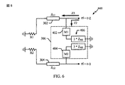
[0027] 図6は、ポート2および3に関して、新規の分配器/結合器300の典型的な偶数モードの説明600を示している。ポート2に関して、送信ライン302、304および整合回路402、404および406のインピダンスは、所望のインピダンス値を得るため、ポート2において見られるインピダンス(Z2およびZ3)が、並列結合を形成するように構成される。例えば、ポート2における所望のインピダンスが、50オームである場合、インピダンスZ2およびZ3の並列結合は、下記のように50オームに設定される。
FIG. 6 shows an exemplary even
50 = Z2 II Z3 (Z2とZ3の並列結合)
[0028] したがって、送信ライン302および304のサイズは、ポート2において、所望の結合されたインピダンスを達成するために整合回路402、404および406のインピダンスを調整することにより、減少され得る。その結果、送信ライン302および304は、より小さなインピダンスを提供し、および対応するより小さなサイズを有するために、設定され得る。
50 = Z2 II Z3 (parallel connection of Z2 and Z3)
[0028] Thus, the size of
[奇数モード解析]
[0029] 図7は、ポート2および3に関して、新規の分配器/結合器300の典型的な奇数モードの説明700を示している。ポート2に関して、整合回路406は、0インピダンスを持つように設定され、および、したがって、接地への短絡と置き換えられる。伝送路302、304および整合回路402、404のインピダンスは、所望のインピダンス値を得るため、ポート2において見られるインピダンス(Z4およびZ5)が、並列結合を形成するように構成される。例えば、ポート2における所望のインピダンスが、50オームである場合、インピダンスZ4およびZ5の並列結合は、下記のように50オームに設定される。
[Odd mode analysis]
FIG. 7 shows an exemplary
50 = Z4 II Z5 (Z4とZ5の並列結合)
[0030] したがって、新規の分配器/結合器300は、送信ライン302、304のインピダンスを減少し、およびそれによって送信ライン302および304の必要なチップ領域を減少するために整合回路402、404および406のインピダンスを調整することにより構成され得る。分配器/結合器300は、また、図2に示される分配器/結合器200と比較して、より大きなレイアウトフレキシビリティを提供するためにポート2と3の間のポート間隔を増加させるように構成される。
50 = Z4 II Z5 (parallel connection of Z4 and Z5)
[0030] Accordingly, the novel distributor /
[0031] 図8は、分配器/結合器配置800の典型的な実施態様を示している。各配置において、ポート1は、送信ライン802によりポート2に連結されており、また、ポート1は、送信ライン804によりポート3に連結されている。第1の整合回路806は、ポート2とノード812の間に連結されており、また、第2の整合回路812は、ポート3とノード812の間に連結されている。第3の整合回路810は、ノード812と接地の間に連結されている。
FIG. 8 shows an exemplary embodiment of a distributor /
[0032] 様々な配置において、整合回路806、808、および810は、送信ライン、インダクタ、キャパシタおよび/または抵抗器を備える。例えば、整合回路806aは、送信ラインとキャパシタを備え、整合回路806bは、送信ラインとインダクタを傷つけ、および、整合回路806cは、送信ラインと抵抗器を備える。整合回路806および808は、送信ラインを備える必要がないことは注目されるべきである。例えば、整合回路806hおよび808hは、キャパシタのみを備える。
[0032] In various arrangements, the matching circuits 806, 808, and 810 comprise transmission lines, inductors, capacitors, and / or resistors. For example, the
[0033] 図8に示される全ての新規の分配器/結合器配置は、送信ライン802および804の必要なチップ領域を減少し、および、図2に示される分配器/結合器200と比較して、より大きなレイアウトフレキシビリティを提供するためにポート2と3の間のポート間隔を増加させるために整合回路806、808および810のインピダンスを調整することにより構成され得る。
[0033] All new distributor / combiner arrangements shown in FIG. 8 reduce the required chip area of transmission lines 802 and 804 and compare to the distributor /
[0034] 図9は、分配器/結合器装置900の典型的な実施態様を示している。例えば、装置900は、図4に示される分配器/結合器300、または図1に示される分配器/結合器108としての使用に適している。態様において、装置900は、本明細書に記述されたように、機能を提供するように構成された1つまたは複数のモジュールによって実装される。例えば、一態様において、各モジュールは、ハードウェアおよび/またはハードウェア実行ソフトウェアを備える。
FIG. 9 illustrates an exemplary embodiment of a distributor /
[0035] 装置900は、第2と第3のポートに連結された第1のポートを有する3ポート回路を提供するための手段(902)を備える第1のモジュールを備え、それは、態様においてパワー分配器/結合器300を備える。
[0035] The
[0036] 装置900は、第2と第3のポートを接地に連結するように構成された整合するための手段(904)を備える第2のモジュールを備え、それは、態様において整合回路306を備える。
[0036] The
[0037] 装置900、整合するための手段904は、第1のポートを第2のポートに連結するための手段(906)を備える第3のモジュールを備え、それは、態様において送信ライン302を備える。
[0037] The
[0038] 装置900、整合するための手段904は、第3のポートを第1のポートに連結するための手段(908)を備える第4のモジュールも備え、それは、態様において送信ライン304を備える。
[0038] The
[0039] 装置900、整合するための手段904は、第2のポートを第1のノードに連結するための手段(910)を備える第5のモジュールも備え、それは、態様において整合回路402を備える。
[0039] The
[0040] 装置900、整合するための手段904は、第1のノードを第3のポートに連結するための手段(912)を備える第6のモジュールも備え、それは、態様において整合回路404を備える。
[0040] The
[0041] 装置900、整合するための手段904は、接地を第1のノードに連結するための手段(914)を備える第7のモジュールも備え、それは、態様において整合回路406を備える。
[0041] The
[0042] 当業者は、情報および信号は、異なる技術および技法のうちの任意の種類を使用して表され、または処理され得ることを、理解するであろう。例えば、上記の説明を通して参照されうるデータ、命令群、コマンド、情報、信号、ビット、シンボル、およびチップは、電圧、電流、電磁波、磁界あるいは磁気粒子、光学界または光学粒子、またはそれら任意の組み合わせによって表わされ得る。トランジスタタイプおよび技術は、同じ結果を獲得するために置き換えられ、再配列され、またはそうでなければ修正され得ることはさらに注目される。例えば、PMOSトランジスタを利用して示された回路は、NMOSトランジスタを使用するために修正され得、その逆もまた同様である。従って、本明細書で開示された増幅器は、様々なトランジスタタイプおよび技術を使用して実現され得、図面で説明されるそれらのトランジスタタイプおよび技術に限定されない。例えば、BJT、GaAs、MOSFET、または任意の他のトランジスタ技術のようなトランジスタタイプが使用され得る。 [0042] Those skilled in the art will understand that information and signals may be represented or processed using any of a variety of different technologies and techniques. For example, data, instructions, commands, information, signals, bits, symbols, and chips that can be referred to throughout the above description are voltages, currents, electromagnetic waves, magnetic fields or magnetic particles, optical fields or optical particles, or any combination thereof Can be represented by It is further noted that transistor types and technologies can be replaced, rearranged or otherwise modified to achieve the same result. For example, a circuit shown utilizing a PMOS transistor can be modified to use an NMOS transistor, and vice versa. Thus, the amplifiers disclosed herein can be implemented using a variety of transistor types and technologies and are not limited to those transistor types and technologies described in the drawings. For example, transistor types such as BJT, GaAs, MOSFET, or any other transistor technology may be used.
[0043]当業者はさらに、本明細書において開示された実施態様に関連して表現された様々な実例となる論理ブロック、モジュール、回路、アルゴリズムステップが、電子ハードウェア、コンピュータソフトウェア、または両方の組み合わせとして実装されうることを認識するだろう。ハードウェアおよびソフトウェアのこの互換性を明確に説明するために、多様な実例となるコンポーネント、ブロック、モジュール、回路、およびステップが、概してそれらの機能の観点から上記で説明されている。このような機能が、ハードウェアとして実装されるか、あるいはソフトウェアとして実装されるかは、特定のアプリケーションおよびシステム全体に課せられる設計制約に依存する。当業者は、各特定のアプリケーションに関して様々な方法で、説明された機能性を実装し得るが、そのような実装の決定は、本発明の典型的な実施態様の範囲から逸脱を引き起こすとして解釈されるべきでない。 [0043] Those of ordinary skill in the art may further note that the various illustrative logic blocks, modules, circuits, algorithm steps expressed in connection with the embodiments disclosed herein are electronic hardware, computer software, or both. You will recognize that it can be implemented as a combination. To clearly illustrate this interchangeability of hardware and software, various illustrative components, blocks, modules, circuits, and steps have been described above generally in terms of their functionality. Whether such functions are implemented as hardware or software depends on specific applications and design constraints imposed on the entire system. Those skilled in the art may implement the described functionality in a variety of ways for each particular application, but such implementation decisions are interpreted as causing deviations from the scope of exemplary embodiments of the invention. Should not.
[0044] 本明細書において開示された実施態様に関連して表現された様々な実例となる論理ブロック、モジュール、および回路は、汎用プロセッサ、デジタル信号プロセッサ(DSP)、特定用途向け集積回路(ASIC)、フィールドプログラマブルゲートアレイ(FPGA)または他のプログラマブル論理デバイス、ディスクリートゲートまたはトランジスタロジック、ディスクリートハードウェアコンポーネント、あるいは本明細書に説明された機能を実行するようにデザインされたそれらの任意の組み合わせで実装または実行され得る。汎用プロセッサはマイクロプロセッサでありうるが、代替としてプロセッサは任意の従来のプロセッサ、コントローラ、マイクロコントローラ、またはステートマシンでありうる。プロセッサはまた、例えば、DSPとマイクロプロセッサ、複数のマイクロプロセッサ、DSPコアと連結した1つまたは複数のマイクロプロセッサ、あるいはその他任意のこのような構成の組み合わせである、コンピューティングデバイスの組み合わせとして実装され得る。 [0044] Various illustrative logic blocks, modules, and circuits expressed in connection with the embodiments disclosed herein are general purpose processors, digital signal processors (DSPs), application specific integrated circuits (ASICs). ), Field programmable gate array (FPGA) or other programmable logic device, discrete gate or transistor logic, discrete hardware components, or any combination thereof designed to perform the functions described herein Can be implemented or implemented. A general purpose processor may be a microprocessor, but in the alternative, the processor may be any conventional processor, controller, microcontroller, or state machine. The processor is also implemented as a combination of computing devices, eg, a DSP and microprocessor, a plurality of microprocessors, one or more microprocessors coupled to a DSP core, or any other combination of such configurations. obtain.
[0045] 本明細書において開示された実施態様に関連して表現されたアルゴリズムまたは方法のステップは、直接ハードウェアにおいて、プロセッサによって実行されるソフトウェアモジュールにおいて、またはこれら2つの組み合わせにおいて、具体化され得る。ソフトウェアモジュールは、ランダムアクセスメモリ(RAM)、フラッシュメモリ、読み出し専用メモリ(ROM)、電気的プログラマブルROM(EPROM)、電気的消去可能プログラマブルROM(EEPROM(登録商標))、レジスタ、ハードディスク、リムーバルディスク、CD−ROM、または当該技術分野において周知である任意の他の形態の記憶媒体において存在し得る。典型的な記憶媒体は、プロセッサがこの記憶媒体から情報を読み取り、またこの記憶媒体に情報を書き込むことができるように、プロセッサに連結される。代替においては、記憶媒体はプロセッサに統合され得る。プロセッサおよび記憶媒体はASICに存在し得る。ASICは、ユーザ端末内に存在し得る。代替として、プロセッサおよび記憶媒体は、ユーザ端末内にディスクリートコンポーネントとして存在し得る。 [0045] Algorithm or method steps expressed in connection with the embodiments disclosed herein may be embodied directly in hardware, in software modules executed by a processor, or in a combination of the two. obtain. Software modules include random access memory (RAM), flash memory, read only memory (ROM), electrically programmable ROM (EPROM), electrically erasable programmable ROM (EEPROM (registered trademark)), registers, hard disk, removable disk, It may reside on a CD-ROM or any other form of storage medium that is well known in the art. An exemplary storage medium is coupled to the processor such that the processor can read information from, and write information to, the storage medium. In the alternative, the storage medium may be integral to the processor. The processor and the storage medium may reside in an ASIC. The ASIC may be present in the user terminal. In the alternative, the processor and the storage medium may reside as discrete components in a user terminal.
[0046] 1つまたは複数の典型的な実施態様において、記述された機能は、ハードウェア、ソフトウェア、ファームウェア、またはそれらの任意の組み合わせに実装され得る。ソフトウェアで実装される場合、これら機能は、コンピュータ可読媒体上で、1つまたは複数の命令またはコードとして送信または記憶され得る。コンピュータ可読媒体は、1つの場所から別の場所へのコンピュータプログラムの転送を促進する任意の媒体を含む非一時的なコンピュータ記憶媒体および通信媒体の双方を含む。非一時的な記憶媒体は、コンピュータによってアクセスされ得る任意の利用可能な媒体であり得る。限定ではなく例として、このようなコンピュータ可読媒体は、RAM、ROM、EEPROM(登録商標)、CD−ROMまたは他の光ディスク記憶装置、磁気ディスク記憶装置またはその他の磁気記憶デバイス、または、データ構造または命令の形式で所望のプログラムコードを記憶または伝送するために使用され得、およびコンピュータによってアクセスされ得る他の任意の媒体を備え得る。また、任意の接続は、コンピュータ可読媒体と厳密には称され得る。例えば、ソフトウェアがウェブサイト、サーバ、または他の遠隔ソースから、同軸ケーブル、光ファイバーケーブル、ツイストペア、デジタル加入者回線(DSL)、あるいは赤外線、無線、およびマイクロ波のようなワイヤレス技法を使用して送信される場合、同軸ケーブル、光ファイバーケーブル、ツイストペア、DSL、あるいは赤外線、無線、およびマイクロ波のようなワイヤレス技法は、媒体の定義に含まれる。ここで使用される場合、ディスク(disk)およびディスク(disc)は、コンパクトディスク(CD)、レーザーディスク(登録商標)、光ディスク、デジタル多目的ディスク(DVD)、フロッピー(登録商標)ディスクおよびブルーレイ(登録商標)ディスクを含み、ここでディスク(disks)は、通常磁気的にデータを再生し、一方、ディスク(discs)は、レーザーを用いて光学的にデータを再生する。上記の組み合わせもまた、コンピュータ可読媒体の範囲内に含まれるべきである。 [0046] In one or more exemplary embodiments, the functions described may be implemented in hardware, software, firmware, or any combination thereof. If implemented in software, the functions may be transmitted or stored as one or more instructions or code on a computer-readable medium. Computer-readable media includes both non-transitory computer storage media and communication media including any medium that facilitates transfer of a computer program from one place to another. A non-transitory storage medium may be any available medium that can be accessed by a computer. By way of example, and not limitation, such computer readable media can be RAM, ROM, EEPROM®, CD-ROM or other optical disk storage device, magnetic disk storage device or other magnetic storage device, or data structure or Any other medium that can be used to store or transmit the desired program code in the form of instructions and that can be accessed by a computer can be provided. Any connection may also be referred to strictly as a computer readable medium. For example, software transmits from a website, server, or other remote source using coaxial cable, fiber optic cable, twisted pair, digital subscriber line (DSL), or wireless techniques such as infrared, wireless, and microwave Where done, coaxial cable, fiber optic cable, twisted pair, DSL, or wireless techniques such as infrared, radio, and microwave are included in the definition of the medium. As used herein, disk and disc are compact disc (CD), laser disc (registered trademark), optical disc, digital multipurpose disc (DVD), floppy (registered trademark) disc, and Blu-ray (registered). (Trademark) discs, where the discs typically reproduce data magnetically, while the discs optically reproduce data using a laser. Combinations of the above should also be included within the scope of computer-readable media.
[0047] 開示された典型的な実施態様の説明は、任意の当業者に、本発明の製造または使用を可能にするように提供される。これらの典型的な実施態様への様々な修正は、当業者にとって容易に明らかであり、ここに定義された一般的な原理は、本発明の精神または範囲から逸脱することなく、他の実施態様にも適用されうる。したがって、本発明は、本明細書に示された典型的な実施態様に限定されるようには意図されず、本明細書に開示された原理および新規な特徴と一致する最も広い範囲を与えられることとなる。
以下に、出願当初の特許請求の範囲に記載された発明を付記する。
[C1]
第2のおよび第3のポートに連結された第1のポートを持つ3つのポート回路と、接地に前記第2のおよび第3のポートを連結するように構成された整合回路とを備えた装置。
[C2]
前記整合回路は、第1のノードと前記第2のポートとの間に連結された第1の整合回路と、前記第1のノードと前記第3のポートとの間に連結された第2の整合回路、および、前記第1のノードと接地との間に連結された第3の整合回路を備えるC1に記載の装置。
[C3]
前記第1のポートと前記第2のポートとの間に連結された第1の送信ラインおよび、前記第1のポートと前記第3のポートとの間に連結された第2の送信ラインをさらに備える、C2に記載の装置。
[C4]
前記第1のおよび第2の送信ライン、および前記第1の、第2のおよび第3の整合回路は、選択された特性インピダンス値に整合された前記第1のポートにおいて見られる結合されたインピダンス値を提供するように構成された、C3に記載の装置。
[C5]
前記選択された特性インピダンス値は、50オームに設定されたC4に記載の装置。
[C6]
前記第1の、第2のおよび第3の整合回路は、前記第1のおよび第2の送信ラインのサイズを調整するように構成されたC3に記載の装置。
[C7]
前記第1のおよび第2の整合回路は、前記第2のおよび第3のポートとの間の間隔を増加させるように構成されたC2に記載の装置。
[C8]
前記第1のおよび第2の送信ライン、および前記第1の、第2のおよび第3の整合回路は、選択された特性インピダンス値に整合された前記第2のポートにおいて見られる結合されたインピダンス値を提供するように構成された、C3に記載の装置。
[C9]
前記選択された特性インピダンス値は、50オームに設定されたC8に記載の装置。
[C10]
前記装置は、双方向の受動的なパワー結合器/分配器を形成するC1に記載の装置。
[C11]
前記双方向の受動的なパワー結合器/分配器は、トランシーバにおける使用のために構成されるC10に記載の装置。
[C12]
第2のおよび第3のポートに連結された第1のポートを持つ3つのポート回路を提供するための手段と、接地に前記第2のおよび第3のポートを連結するように構成された整合するための手段とを備えた装置。
[C13]
整合するための前記手段は、第1のノードと前記第2のポートとを連結するための手段と、前記第1のノードと前記第3のポートとを連結するための手段と、前記第1のノードに接地を連結するための手段とを備えるC12に記載の装置。
[C14]
前記第1のおよび第2のポートとの間に第1の送信ラインを連結するための手段および、第1のおよび第3のポートとの間に第2の送信ラインを連結するための手段をさらに備える、C13に記載の装置。
[C15]
前記第1の送信ライン、前記第2の送信ライン、前記第2のポートを連結するための前記手段、前記第1のノードを連結するための前記手段、および、前記接地を連結するための前記手段は、選択された特性インピダンス値に整合された前記第1のポートにおいて見られる結合されたインピダンス値を提供するように構成された、C14に記載の装置。
[C16]
前記第2のポートを連結するための前記手段、前記第1のノードを連結するための前記手段、および、前記接地を連結するための前記手段は、前記第1のおよび第2の送信ラインのサイズを調整するように構成されたC14に記載の装置。
[C17]
前記第2のポートを連結するための前記手段、前記第1のノードを連結するための前記手段は、前記第2のおよび第3のポートとの間の間隔を増加させるように構成されたC14に記載の装置。
[C18]
前記第1の送信ライン、前記第2の送信ライン、前記第2のポートを連結するための前記手段、前記第1のノードを連結するための前記手段、および、前記接地を連結するための前記手段は、選択された特性インピダンス値に整合された前記第2のポートにおいて見られる結合されたインピダンス値を提供するように構成された、C14に記載の装置。
[C19]
前記装置は、双方向の受動的なパワー結合器/分配器を形成するC12に記載の装置。
[C20]
前記双方向の受動的なパワー結合器/分配器は、トランシーバにおける使用のために構成されるC19に記載の装置。
[0047] The description of the disclosed exemplary embodiments is provided to enable any person skilled in the art to make or use the present invention. Various modifications to these exemplary embodiments will be readily apparent to those skilled in the art, and the general principles defined herein may be used in other embodiments without departing from the spirit or scope of the invention. It can also be applied to. Accordingly, the present invention is not intended to be limited to the exemplary embodiments shown herein but is to be accorded the widest scope consistent with the principles and novel features disclosed herein. It will be.
The invention described in the scope of claims at the beginning of the application will be appended.
[C1]
An apparatus comprising a three port circuit having a first port coupled to a second and third port, and a matching circuit configured to couple the second and third port to ground .
[C2]
The matching circuit includes a first matching circuit connected between a first node and the second port, and a second matching circuit connected between the first node and the third port. The apparatus of C1, comprising a matching circuit and a third matching circuit coupled between the first node and ground.
[C3]
A first transmission line coupled between the first port and the second port; and a second transmission line coupled between the first port and the third port. The apparatus of C2, comprising.
[C4]
The first and second transmission lines, and the first, second and third matching circuits are coupled impedances found at the first port that are matched to a selected characteristic impedance value. The device of C3, configured to provide a value.
[C5]
The apparatus of C4, wherein the selected characteristic impedance value is set to 50 ohms.
[C6]
The apparatus of C3, wherein the first, second and third matching circuits are configured to adjust a size of the first and second transmission lines.
[C7]
The apparatus of C2, wherein the first and second matching circuits are configured to increase a spacing between the second and third ports.
[C8]
The first and second transmission lines, and the first, second and third matching circuits are coupled impedances found at the second port that are matched to a selected characteristic impedance value. The device of C3, configured to provide a value.
[C9]
The apparatus of C8, wherein the selected characteristic impedance value is set to 50 ohms.
[C10]
The apparatus of C1, wherein the apparatus forms a bidirectional passive power combiner / distributor.
[C11]
The apparatus of C10, wherein the bidirectional passive power combiner / distributor is configured for use in a transceiver.
[C12]
Means for providing a three-port circuit having a first port coupled to the second and third ports, and a match configured to couple the second and third ports to ground And means for performing.
[C13]
The means for matching includes means for connecting a first node and the second port, means for connecting the first node and the third port, and the first And the means for connecting ground to the node of C12.
[C14]
Means for connecting a first transmission line between the first and second ports and means for connecting a second transmission line between the first and third ports; The apparatus according to C13, further comprising:
[C15]
Said first transmission line; said second transmission line; said means for connecting said second port; said means for connecting said first node; and said means for connecting said ground The apparatus of C14, wherein the means is configured to provide a combined impedance value found at the first port that is matched to a selected characteristic impedance value.
[C16]
The means for connecting the second port, the means for connecting the first node, and the means for connecting the ground are: the first and second transmission lines. The apparatus according to C14, configured to adjust a size.
[C17]
The means for connecting the second port and the means for connecting the first node are configured to increase the spacing between the second and third ports. The device described in 1.
[C18]
Said first transmission line; said second transmission line; said means for connecting said second port; said means for connecting said first node; and said means for connecting said ground The apparatus of C14, wherein the means is configured to provide a combined impedance value found at the second port that is matched to a selected characteristic impedance value.
[C19]
The apparatus of C12, wherein the apparatus forms a bidirectional passive power combiner / distributor.
[C20]
The apparatus of C19, wherein the bidirectional passive power combiner / distributor is configured for use in a transceiver.
Claims (7)
第2のおよび第3のポートに連結された第1のポートを持つ3つのポート回路を提供するための手段と、
接地に前記第2のおよび第3のポートを連結するように構成された整合するための手段とを備え、
整合するための前記手段は、
第1のノードと前記第2のポートとの間に連結された整合するための第1の手段と、
前記第1のノードと前記第3のポートとの間に連結された整合するための第2の手段と、
前記第1のノードと接地との間に連結された整合するための第3の手段とを備え、
前記装置はさらに、
前記第1のおよび第2のポートとの間を連結するための手段としての第1の送信ラインと、
第1のおよび第3のポートとの間を連結するための手段としての第2の送信ラインとを備え、
前記第1の送信ライン、前記第2の送信ライン、整合するための前記第1の手段、整合するための前記第2の手段、および、整合するための前記第3の手段のインピダンスは、第1の選択された特性インピダンス値に整合するように結合され、および、前記第1のポートにおいて、第1の結合されたインピダンス値が得られるように結合され、
前記第1のポートにおいて、前記第1の結合されたインピダンス値を得るために、整合するための前記第1の手段、整合するための前記第2の手段、および、整合するための前記第3の手段のインピダンスが調整される、装置。 A device,
Means for providing a three port circuit having a first port coupled to the second and third ports;
Means for matching configured to couple the second and third ports to ground; and
Said means for matching is:
A first means for matching coupled between a first node and the second port;
A second means for matching coupled between the first node and the third port;
A third means for matching coupled between the first node and ground;
The apparatus further includes:
A first transmission line as a means for connecting between the first and second ports;
A second transmission line as a means for connecting between the first and third ports;
Said first transmission line, the second transmission line, said first means for aligning said second means for matching, and impedance of said third means for matching, the coupled to match the first selected characteristic impedance value, and, in the first port, is coupled to the first combined impedance value is obtained,
In the first port, the first means for matching, the second means for matching, and the third for matching to obtain the first combined impedance value. The device in which the impedance of the means is adjusted .
Applications Claiming Priority (3)
| Application Number | Priority Date | Filing Date | Title |
|---|---|---|---|
| US13/678,277 | 2012-11-15 | ||
| US13/678,277 US9373879B2 (en) | 2012-11-15 | 2012-11-15 | Compact power divider/combiner with flexible output spacing |
| PCT/US2013/069753 WO2014078334A1 (en) | 2012-11-15 | 2013-11-12 | Compact power divider/combiner with flexible output spacing |
Publications (3)
| Publication Number | Publication Date |
|---|---|
| JP2015535162A JP2015535162A (en) | 2015-12-07 |
| JP2015535162A5 JP2015535162A5 (en) | 2016-12-08 |
| JP6316836B2 true JP6316836B2 (en) | 2018-04-25 |
Family
ID=49766148
Family Applications (1)
| Application Number | Title | Priority Date | Filing Date |
|---|---|---|---|
| JP2015542731A Active JP6316836B2 (en) | 2012-11-15 | 2013-11-12 | Compact power distributor / combiner with flexible output spacing |
Country Status (5)
| Country | Link |
|---|---|
| US (1) | US9373879B2 (en) |
| EP (1) | EP2920841B1 (en) |
| JP (1) | JP6316836B2 (en) |
| CN (1) | CN104798249B (en) |
| WO (1) | WO2014078334A1 (en) |
Families Citing this family (8)
| Publication number | Priority date | Publication date | Assignee | Title |
|---|---|---|---|---|
| US9264012B2 (en) * | 2012-06-25 | 2016-02-16 | Ppc Broadband, Inc. | Radio frequency signal splitter |
| US9831837B2 (en) | 2014-11-05 | 2017-11-28 | Qualcomm Incorporated | Dynamic power divider circuits and methods |
| WO2016151726A1 (en) * | 2015-03-23 | 2016-09-29 | 株式会社日立国際電気 | Wilkinson combiner and wilkinson divider |
| CN106154191B (en) | 2015-04-16 | 2020-06-16 | 通用电气公司 | Magnetic resonance imaging device, power amplifier module and power synthesizer |
| US10910714B2 (en) | 2017-09-11 | 2021-02-02 | Qualcomm Incorporated | Configurable power combiner and splitter |
| CN108011168B (en) * | 2017-11-09 | 2019-12-13 | 西安电子科技大学 | Novel Wilkinson power divider capable of terminating complex impedance |
| KR102293253B1 (en) * | 2018-12-24 | 2021-08-26 | 충남대학교산학협력단 | Phase-shiftable power divider/combiner |
| CN113540738A (en) * | 2020-04-15 | 2021-10-22 | 深圳市大富科技股份有限公司 | Wilkinson power divider and PCB |
Family Cites Families (14)
| Publication number | Priority date | Publication date | Assignee | Title |
|---|---|---|---|---|
| JPS583602U (en) * | 1981-06-30 | 1983-01-11 | 日本電気株式会社 | power divider |
| JPS59176903A (en) * | 1983-03-25 | 1984-10-06 | Fujitsu Ltd | Power distributing and synthesizing device |
| FR2638571B1 (en) * | 1988-10-27 | 1990-11-30 | Alcatel Transmission | DEVICE FOR CORRECTING GROUP PROPAGATION TIME IN MICROWAVE |
| US6005442A (en) | 1996-03-26 | 1999-12-21 | Matsushita Electric Industrial Co., Ltd. | Divider/combiner |
| US5847625A (en) | 1997-04-02 | 1998-12-08 | Tx Rx Systems Inc. | Power Divider directional coupler |
| JP2000106501A (en) | 1998-09-28 | 2000-04-11 | Matsushita Electric Ind Co Ltd | Power distribution circuit and power synthesizing circuit |
| JP2000124712A (en) * | 1998-10-16 | 2000-04-28 | Nippon Antenna Co Ltd | Concentrated constant type wilkinson circuit |
| JP3430416B2 (en) * | 1999-04-16 | 2003-07-28 | 横河電機株式会社 | Power distributor |
| JP2000307313A (en) | 1999-04-16 | 2000-11-02 | Mitsubishi Electric Corp | Power distributor combiner |
| JP2007019827A (en) * | 2005-07-07 | 2007-01-25 | Toshiba Corp | Transmission/reception module |
| US7961063B2 (en) * | 2008-07-31 | 2011-06-14 | Freescale Semiconductor, Inc. | Balun signal transformer and method of forming |
| US8482364B2 (en) | 2009-09-13 | 2013-07-09 | International Business Machines Corporation | Differential cross-coupled power combiner or divider |
| CN102637938B (en) * | 2011-02-15 | 2014-10-22 | 中国科学院微电子研究所 | Double-frequency power divider and design method thereof |
| US8698576B2 (en) * | 2011-04-27 | 2014-04-15 | Alcatel Lucent | Isolated zero degree reactive radio frequency high power combiner |
-
2012
- 2012-11-15 US US13/678,277 patent/US9373879B2/en active Active
-
2013
- 2013-11-12 CN CN201380059282.6A patent/CN104798249B/en active Active
- 2013-11-12 JP JP2015542731A patent/JP6316836B2/en active Active
- 2013-11-12 EP EP13805976.1A patent/EP2920841B1/en active Active
- 2013-11-12 WO PCT/US2013/069753 patent/WO2014078334A1/en active Application Filing
Also Published As
| Publication number | Publication date |
|---|---|
| WO2014078334A1 (en) | 2014-05-22 |
| CN104798249A (en) | 2015-07-22 |
| EP2920841B1 (en) | 2019-10-30 |
| US9373879B2 (en) | 2016-06-21 |
| US20140132364A1 (en) | 2014-05-15 |
| JP2015535162A (en) | 2015-12-07 |
| CN104798249B (en) | 2019-04-09 |
| EP2920841A1 (en) | 2015-09-23 |
Similar Documents
| Publication | Publication Date | Title |
|---|---|---|
| JP6316836B2 (en) | Compact power distributor / combiner with flexible output spacing | |
| JP6017577B2 (en) | Impedance balance for blocking between transmitter and receiver | |
| JP5922315B2 (en) | Parallel hybrid matching network | |
| US20130147664A1 (en) | Reconfigurable millimeter wave multibeam antenna array | |
| US9319021B2 (en) | Digitally controlled phase shifter | |
| JP5956091B2 (en) | Amplifier with switchable common gate gain buffer | |
| JP6311785B2 (en) | High frequency front end circuit | |
| US10700655B2 (en) | Gain-dependent impedance matching and linearity | |
| JP2015046895A (en) | Configurable antenna interface | |
| JP6208367B2 (en) | Adjustable load line | |
| US9026060B2 (en) | Bidirectional matching network | |
| JP6109849B2 (en) | Millimeter wave power amplifier | |
| US8723602B2 (en) | Method and apparatus for a class-E load tuned beamforming 60 GHz transmitter | |
| JP2013157981A (en) | Signal combining circuit and system | |
| US20230030569A1 (en) | Signal power splitter/combiner with resistance and impedance transformer loading | |
| WO2020112283A1 (en) | Gain-dependent impedance matching and linearity |
Legal Events
| Date | Code | Title | Description |
|---|---|---|---|
| A521 | Request for written amendment filed |
Free format text: JAPANESE INTERMEDIATE CODE: A523 Effective date: 20161018 |
|
| A621 | Written request for application examination |
Free format text: JAPANESE INTERMEDIATE CODE: A621 Effective date: 20161018 |
|
| A131 | Notification of reasons for refusal |
Free format text: JAPANESE INTERMEDIATE CODE: A131 Effective date: 20171010 |
|
| A521 | Request for written amendment filed |
Free format text: JAPANESE INTERMEDIATE CODE: A523 Effective date: 20180110 |
|
| TRDD | Decision of grant or rejection written | ||
| A01 | Written decision to grant a patent or to grant a registration (utility model) |
Free format text: JAPANESE INTERMEDIATE CODE: A01 Effective date: 20180227 |
|
| A61 | First payment of annual fees (during grant procedure) |
Free format text: JAPANESE INTERMEDIATE CODE: A61 Effective date: 20180328 |
|
| R150 | Certificate of patent or registration of utility model |
Ref document number: 6316836 Country of ref document: JP Free format text: JAPANESE INTERMEDIATE CODE: R150 |
|
| R250 | Receipt of annual fees |
Free format text: JAPANESE INTERMEDIATE CODE: R250 |
|
| R250 | Receipt of annual fees |
Free format text: JAPANESE INTERMEDIATE CODE: R250 |
|
| R250 | Receipt of annual fees |
Free format text: JAPANESE INTERMEDIATE CODE: R250 |