JP6301259B2 - Semiconductor substrate and formation method - Google Patents
Semiconductor substrate and formation method Download PDFInfo
- Publication number
- JP6301259B2 JP6301259B2 JP2014542554A JP2014542554A JP6301259B2 JP 6301259 B2 JP6301259 B2 JP 6301259B2 JP 2014542554 A JP2014542554 A JP 2014542554A JP 2014542554 A JP2014542554 A JP 2014542554A JP 6301259 B2 JP6301259 B2 JP 6301259B2
- Authority
- JP
- Japan
- Prior art keywords
- base layer
- mask
- layer
- growth
- less
- Prior art date
- Legal status (The legal status is an assumption and is not a legal conclusion. Google has not performed a legal analysis and makes no representation as to the accuracy of the status listed.)
- Active
Links
- 238000000034 method Methods 0.000 title claims description 126
- 239000000758 substrate Substances 0.000 title claims description 98
- 230000015572 biosynthetic process Effects 0.000 title claims description 48
- 239000004065 semiconductor Substances 0.000 title claims description 39
- 239000000463 material Substances 0.000 claims description 97
- 230000008569 process Effects 0.000 claims description 93
- 238000005530 etching Methods 0.000 claims description 43
- 239000010409 thin film Substances 0.000 claims description 32
- 239000010703 silicon Substances 0.000 claims description 23
- 229910052710 silicon Inorganic materials 0.000 claims description 23
- JMASRVWKEDWRBT-UHFFFAOYSA-N Gallium nitride Chemical compound [Ga]#N JMASRVWKEDWRBT-UHFFFAOYSA-N 0.000 claims description 22
- 229910002601 GaN Inorganic materials 0.000 claims description 20
- 230000007704 transition Effects 0.000 claims description 12
- QGZKDVFQNNGYKY-UHFFFAOYSA-N Ammonia Chemical compound N QGZKDVFQNNGYKY-UHFFFAOYSA-N 0.000 claims description 10
- 230000007547 defect Effects 0.000 claims description 9
- 150000004767 nitrides Chemical class 0.000 claims description 9
- 229910052594 sapphire Inorganic materials 0.000 claims description 9
- 239000010980 sapphire Substances 0.000 claims description 9
- 238000000926 separation method Methods 0.000 claims description 8
- 229910052733 gallium Inorganic materials 0.000 claims description 7
- GYHNNYVSQQEPJS-UHFFFAOYSA-N Gallium Chemical compound [Ga] GYHNNYVSQQEPJS-UHFFFAOYSA-N 0.000 claims description 6
- VEXZGXHMUGYJMC-UHFFFAOYSA-N Hydrochloric acid Chemical compound Cl VEXZGXHMUGYJMC-UHFFFAOYSA-N 0.000 claims description 6
- 229910052581 Si3N4 Inorganic materials 0.000 claims description 6
- 229910052739 hydrogen Inorganic materials 0.000 claims description 6
- 239000001257 hydrogen Substances 0.000 claims description 6
- HQVNEWCFYHHQES-UHFFFAOYSA-N silicon nitride Chemical compound N12[Si]34N5[Si]62N3[Si]51N64 HQVNEWCFYHHQES-UHFFFAOYSA-N 0.000 claims description 6
- 229910021529 ammonia Inorganic materials 0.000 claims description 5
- 238000010494 dissociation reaction Methods 0.000 claims description 5
- 230000005593 dissociations Effects 0.000 claims description 5
- 239000007789 gas Substances 0.000 claims description 5
- 229910000041 hydrogen chloride Inorganic materials 0.000 claims description 5
- IXCSERBJSXMMFS-UHFFFAOYSA-N hydrogen chloride Substances Cl.Cl IXCSERBJSXMMFS-UHFFFAOYSA-N 0.000 claims description 5
- 238000011065 in-situ storage Methods 0.000 claims description 5
- 238000007373 indentation Methods 0.000 claims description 5
- 238000000151 deposition Methods 0.000 claims description 4
- 239000012298 atmosphere Substances 0.000 claims description 3
- 239000000460 chlorine Substances 0.000 claims description 3
- 229910052736 halogen Inorganic materials 0.000 claims description 3
- 150000002367 halogens Chemical class 0.000 claims description 3
- 229910052738 indium Inorganic materials 0.000 claims description 3
- 229910052751 metal Inorganic materials 0.000 claims description 3
- 239000002184 metal Substances 0.000 claims description 3
- 238000002488 metal-organic chemical vapour deposition Methods 0.000 claims description 3
- ZAMOUSCENKQFHK-UHFFFAOYSA-N Chlorine atom Chemical compound [Cl] ZAMOUSCENKQFHK-UHFFFAOYSA-N 0.000 claims description 2
- 229910052782 aluminium Inorganic materials 0.000 claims description 2
- 229910052801 chlorine Inorganic materials 0.000 claims description 2
- 239000002178 crystalline material Substances 0.000 claims description 2
- 150000002431 hydrogen Chemical class 0.000 claims description 2
- 239000000203 mixture Substances 0.000 claims description 2
- 230000008021 deposition Effects 0.000 claims 2
- 239000000126 substance Substances 0.000 claims 1
- XUIMIQQOPSSXEZ-UHFFFAOYSA-N Silicon Chemical compound [Si] XUIMIQQOPSSXEZ-UHFFFAOYSA-N 0.000 description 21
- 239000000376 reactant Substances 0.000 description 11
- QJGQUHMNIGDVPM-UHFFFAOYSA-N nitrogen group Chemical group [N] QJGQUHMNIGDVPM-UHFFFAOYSA-N 0.000 description 9
- 238000006243 chemical reaction Methods 0.000 description 7
- 150000001875 compounds Chemical class 0.000 description 6
- 238000012545 processing Methods 0.000 description 5
- IJGRMHOSHXDMSA-UHFFFAOYSA-N Atomic nitrogen Chemical compound N#N IJGRMHOSHXDMSA-UHFFFAOYSA-N 0.000 description 4
- UFHFLCQGNIYNRP-UHFFFAOYSA-N Hydrogen Chemical compound [H][H] UFHFLCQGNIYNRP-UHFFFAOYSA-N 0.000 description 4
- BLRPTPMANUNPDV-UHFFFAOYSA-N Silane Chemical compound [SiH4] BLRPTPMANUNPDV-UHFFFAOYSA-N 0.000 description 4
- 230000008859 change Effects 0.000 description 4
- 238000005229 chemical vapour deposition Methods 0.000 description 4
- PMHQVHHXPFUNSP-UHFFFAOYSA-M copper(1+);methylsulfanylmethane;bromide Chemical compound Br[Cu].CSC PMHQVHHXPFUNSP-UHFFFAOYSA-M 0.000 description 4
- 239000013078 crystal Substances 0.000 description 4
- 238000010586 diagram Methods 0.000 description 4
- 229910000077 silane Inorganic materials 0.000 description 4
- 229910052799 carbon Inorganic materials 0.000 description 3
- 239000002131 composite material Substances 0.000 description 3
- 238000005137 deposition process Methods 0.000 description 3
- 238000004519 manufacturing process Methods 0.000 description 3
- 238000000927 vapour-phase epitaxy Methods 0.000 description 3
- PNEYBMLMFCGWSK-UHFFFAOYSA-N aluminium oxide Inorganic materials [O-2].[O-2].[O-2].[Al+3].[Al+3] PNEYBMLMFCGWSK-UHFFFAOYSA-N 0.000 description 2
- 238000011161 development Methods 0.000 description 2
- APFVFJFRJDLVQX-UHFFFAOYSA-N indium atom Chemical compound [In] APFVFJFRJDLVQX-UHFFFAOYSA-N 0.000 description 2
- 229910010272 inorganic material Inorganic materials 0.000 description 2
- 239000011147 inorganic material Substances 0.000 description 2
- 229910052757 nitrogen Inorganic materials 0.000 description 2
- 230000000737 periodic effect Effects 0.000 description 2
- 239000012071 phase Substances 0.000 description 2
- JBRZTFJDHDCESZ-UHFFFAOYSA-N AsGa Chemical compound [As]#[Ga] JBRZTFJDHDCESZ-UHFFFAOYSA-N 0.000 description 1
- 229910001218 Gallium arsenide Inorganic materials 0.000 description 1
- 229910004205 SiNX Inorganic materials 0.000 description 1
- XAGFODPZIPBFFR-UHFFFAOYSA-N aluminium Chemical compound [Al] XAGFODPZIPBFFR-UHFFFAOYSA-N 0.000 description 1
- 239000000969 carrier Substances 0.000 description 1
- 238000005136 cathodoluminescence Methods 0.000 description 1
- 239000013626 chemical specie Substances 0.000 description 1
- 238000001739 density measurement Methods 0.000 description 1
- 238000001514 detection method Methods 0.000 description 1
- 238000010894 electron beam technology Methods 0.000 description 1
- 238000005516 engineering process Methods 0.000 description 1
- 230000005669 field effect Effects 0.000 description 1
- 239000010408 film Substances 0.000 description 1
- 239000012467 final product Substances 0.000 description 1
- -1 for example Chemical class 0.000 description 1
- UPWPDUACHOATKO-UHFFFAOYSA-K gallium trichloride Chemical compound Cl[Ga](Cl)Cl UPWPDUACHOATKO-UHFFFAOYSA-K 0.000 description 1
- 150000004820 halides Chemical class 0.000 description 1
- 239000011261 inert gas Substances 0.000 description 1
- 239000007791 liquid phase Substances 0.000 description 1
- 230000007246 mechanism Effects 0.000 description 1
- 238000002844 melting Methods 0.000 description 1
- 230000008018 melting Effects 0.000 description 1
- 150000001247 metal acetylides Chemical class 0.000 description 1
- 229910001507 metal halide Inorganic materials 0.000 description 1
- 150000005309 metal halides Chemical class 0.000 description 1
- 238000012986 modification Methods 0.000 description 1
- 230000004048 modification Effects 0.000 description 1
- 239000012299 nitrogen atmosphere Substances 0.000 description 1
- 229910052756 noble gas Inorganic materials 0.000 description 1
- 150000002835 noble gases Chemical class 0.000 description 1
- 230000005693 optoelectronics Effects 0.000 description 1
- 125000002524 organometallic group Chemical group 0.000 description 1
- 238000000206 photolithography Methods 0.000 description 1
- 238000000197 pyrolysis Methods 0.000 description 1
- 230000009467 reduction Effects 0.000 description 1
- 230000002441 reversible effect Effects 0.000 description 1
- 230000002269 spontaneous effect Effects 0.000 description 1
- 230000001960 triggered effect Effects 0.000 description 1
- 239000012808 vapor phase Substances 0.000 description 1
Images


Classifications
-
- H—ELECTRICITY
- H01—ELECTRIC ELEMENTS
- H01L—SEMICONDUCTOR DEVICES NOT COVERED BY CLASS H10
- H01L21/00—Processes or apparatus adapted for the manufacture or treatment of semiconductor or solid state devices or of parts thereof
- H01L21/02—Manufacture or treatment of semiconductor devices or of parts thereof
- H01L21/02104—Forming layers
- H01L21/02365—Forming inorganic semiconducting materials on a substrate
- H01L21/02367—Substrates
- H01L21/0237—Materials
- H01L21/02387—Group 13/15 materials
- H01L21/02389—Nitrides
-
- H—ELECTRICITY
- H01—ELECTRIC ELEMENTS
- H01L—SEMICONDUCTOR DEVICES NOT COVERED BY CLASS H10
- H01L21/00—Processes or apparatus adapted for the manufacture or treatment of semiconductor or solid state devices or of parts thereof
- H01L21/02—Manufacture or treatment of semiconductor devices or of parts thereof
- H01L21/02104—Forming layers
- H01L21/02365—Forming inorganic semiconducting materials on a substrate
- H01L21/02518—Deposited layers
- H01L21/02521—Materials
- H01L21/02538—Group 13/15 materials
- H01L21/0254—Nitrides
-
- H—ELECTRICITY
- H01—ELECTRIC ELEMENTS
- H01L—SEMICONDUCTOR DEVICES NOT COVERED BY CLASS H10
- H01L21/00—Processes or apparatus adapted for the manufacture or treatment of semiconductor or solid state devices or of parts thereof
- H01L21/02—Manufacture or treatment of semiconductor devices or of parts thereof
- H01L21/02104—Forming layers
- H01L21/02365—Forming inorganic semiconducting materials on a substrate
- H01L21/02612—Formation types
- H01L21/02617—Deposition types
- H01L21/02636—Selective deposition, e.g. simultaneous growth of mono- and non-monocrystalline semiconductor materials
- H01L21/02647—Lateral overgrowth
-
- H—ELECTRICITY
- H01—ELECTRIC ELEMENTS
- H01L—SEMICONDUCTOR DEVICES NOT COVERED BY CLASS H10
- H01L21/00—Processes or apparatus adapted for the manufacture or treatment of semiconductor or solid state devices or of parts thereof
- H01L21/02—Manufacture or treatment of semiconductor devices or of parts thereof
- H01L21/02104—Forming layers
- H01L21/02365—Forming inorganic semiconducting materials on a substrate
- H01L21/02656—Special treatments
- H01L21/02658—Pretreatments
Landscapes
- Engineering & Computer Science (AREA)
- Microelectronics & Electronic Packaging (AREA)
- Condensed Matter Physics & Semiconductors (AREA)
- General Physics & Mathematics (AREA)
- Manufacturing & Machinery (AREA)
- Computer Hardware Design (AREA)
- Physics & Mathematics (AREA)
- Power Engineering (AREA)
- Chemical & Material Sciences (AREA)
- Materials Engineering (AREA)
- Crystals, And After-Treatments Of Crystals (AREA)
- Chemical Vapour Deposition (AREA)
- Drying Of Semiconductors (AREA)
Description
以下は、半導体基板の形成方法、詳細には、マスクを用いる半導体基板の形成方法を対象とする。 The following is directed to a method for forming a semiconductor substrate, specifically, a method for forming a semiconductor substrate using a mask.
窒化ガリウム(GaN)、窒化インジウムガリウム(InGaN)および窒化ガリウムアルミニウム(GaAlN)などの三元化合物、さらに四元化合物(AlGaInN)などの第13−15族材料を含む半導体系化合物は、直接バンドギャップ半導体である。そのような材料は短波長発光の大きな可能性を有すると認識されてきており、そのため、発光ダイオード(LED)、レーザダイオード(LD)、紫外線検出器、および高温電子機器の製造での使用に適している。 A semiconductor compound including a ternary compound such as gallium nitride (GaN), indium gallium nitride (InGaN), and gallium aluminum nitride (GaAlN), and a group 13-15 material such as a quaternary compound (AlGaInN) has a direct band gap. It is a semiconductor. Such materials have been recognized as having great potential for short wavelength light emission and are therefore suitable for use in the manufacture of light emitting diodes (LEDs), laser diodes (LDs), ultraviolet detectors, and high temperature electronics. ing.
しかしながら、そのような半導体材料の開発は、そのような材料の工程、詳細には、オプトエレクトロニクスにおいて短波長発光の製造に必要な材料の高品質な単結晶形の形成、を取り巻く困難性によって阻まれてきた。GaNは自然発生の化合物として見ることができず、そのため、ブール様ケイ素、ガリウムヒ素、またはサファイアから融解し取り出すことができない。というのは、常圧でのその理論的融解温度がその解離温度を超えるためである。別の方法として、業界はエピタキシャル成長プロセスの使用によるバルクGaN結晶の形成に取り組んできた。しかしながら、依然として、適切な低欠陥密度バルクGaN材料の形成に関する問題が残っている。 However, the development of such semiconductor materials is hampered by the difficulties surrounding the process of such materials, particularly the formation of high quality single crystal forms of materials necessary for the production of short wavelength light emission in optoelectronics. It has been rare. GaN cannot be seen as a naturally occurring compound and therefore cannot be melted and extracted from boule-like silicon, gallium arsenide, or sapphire. This is because its theoretical melting temperature at normal pressure exceeds its dissociation temperature. Alternatively, the industry has been working on the formation of bulk GaN crystals by using an epitaxial growth process. However, problems remain with the formation of suitable low defect density bulk GaN materials.
拡張欠陥(貫通転位、積層欠陥、および逆位相境界)の存在は、著しく劣化した性能の原因となり、結果として装置の動作寿命の短縮をもたらす。具体的には、転位は非放射中心としてふるまい、そのため、これらの材料からなる発光ダイオードおよびレーザダイオードの発光効率が低下する。また、これらの転位は暗電流も増加させる。貫通転位は高輝度の発光ダイオードの開発を妨げなかったが、転位は、高電子移動度トランジスタ、電界効果トランジスタ、及び他の電子デバイスなどのp−n接合デバイスにおいて、過剰な逆バイアス漏れ電流を引き起こす。さらに、転位はキャリアに対する強い散乱中心として作用する可能性があり、電子及び正孔の移動度を減少させ、多くの半導体デバイスの性能を制限する。 The presence of extended defects (threading dislocations, stacking faults, and antiphase boundaries) contributes to significantly degraded performance, resulting in a shortened operating life of the device. Specifically, dislocations behave as non-radiative centers, so that the light emission efficiency of light emitting diodes and laser diodes made of these materials is reduced. These dislocations also increase dark current. Although threading dislocations did not hinder the development of high brightness light emitting diodes, dislocations caused excessive reverse bias leakage current in pn junction devices such as high electron mobility transistors, field effect transistors, and other electronic devices. cause. In addition, dislocations can act as strong scattering centers for carriers, reducing electron and hole mobility and limiting the performance of many semiconductor devices.
半導体基板の形成方法は、成長プロセスの間の成長基板上への第13−15族材料のベース層の形成、成長プロセスの間におけるベース層を覆う、マスク領域およびギャップ領域を含んでなるマスクの形成、ならびに成長プロセスの間のマスクに覆われたベース層の一部の優先的除去を含んでなる。 A method of forming a semiconductor substrate includes forming a base layer of a Group 13-15 material on a growth substrate during a growth process, a mask region comprising a mask region and a gap region covering the base layer during the growth process. Forming and preferential removal of a portion of the base layer covered by the mask during the growth process.
その他の態様において、半導体基板の形成方法は、a)成長基板上への第13−15族材料のベース層の形成、b)ベース層を覆う、窒化物材料を含んでなるマスクの形成、ならびにc)マスク形成後の、エッチングおよびベース層およびマスクの一部の優先的除去を含んでなる。前記の工程a)、b)およびc)は、成長チャンバ内での単一操作の間にin−situで実施することができる。 In another aspect, a method for forming a semiconductor substrate comprises: a) forming a base layer of a Group 13-15 material on a growth substrate, b) forming a mask comprising a nitride material covering the base layer, and c) After mask formation, comprising etching and preferential removal of the base layer and part of the mask. Said steps a), b) and c) can be performed in-situ during a single operation in the growth chamber.
別の態様において、半導体基板の形成方法は、成長プロセスの間における、サファイア系ベース基盤を有する成長基盤上へのGaN含有ベース層および成長基盤を覆うバッファ層であって、ベース基盤とベース層との間に配置されるバッファ層の形成を含んでなる。 In another aspect, a method for forming a semiconductor substrate includes a GaN-containing base layer on a growth substrate having a sapphire base substrate and a buffer layer covering the growth substrate during the growth process, the base substrate and the base layer Forming a buffer layer disposed between the two.
本方法は、さらに、ベース層を覆うマスク領域およびマスク領域間のギャップ領域を含んでなるマスクの形成、ならびにマスクに覆われたベース層の一部の優先的除去を含んでなる。 The method further comprises forming a mask comprising a mask region covering the base layer and a gap region between the mask regions, and preferential removal of a portion of the base layer covered by the mask.
添付図面を参照することにより、本開示はよりよく理解され、その多くの特徴および利点は当業者に明らかとなりうる。 The present disclosure is better understood and its numerous features and advantages will become apparent to those skilled in the art by reference to the accompanying drawings.
異なる図面における同じ参照記号の使用は、同様のまたは同一の要素を示す。 The use of the same reference symbols in different drawings indicates similar or identical elements.
以下の説明は包括的には基板材料に関し、詳細には、複数の半導体材料を含んでなる基板、またそれは複数の半導体層(すなわち、半導体基板)を含んでいてもよい基板、及びそのような物品を形成する方法に関する。半導体基板は、例えば、窒化ガリウム(GaN)を含む、第13−15族材料を含むことができる。第13−15族材料を参照することは、IUPAC周期表(2011年1月21日版)に基づいて、元素の周期表の第13族からの少なくとも1つの元素と、元素の周期表の第15族からの少なくとも1つの元素とを含む化合物を含むことは理解されるであろう。 The following description relates generally to substrate materials, and in particular, a substrate comprising a plurality of semiconductor materials, a substrate that may comprise a plurality of semiconductor layers (ie, semiconductor substrates), and such The present invention relates to a method of forming an article. The semiconductor substrate can include a Group 13-15 material including, for example, gallium nitride (GaN). Referencing Group 13-15 materials is based on the IUPAC Periodic Table (January 21, 2011 edition) and includes at least one element from Group 13 of the Periodic Table of Elements and It will be understood to include compounds comprising at least one element from Group 15.
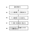
図1は、実施形態による半導体基板材料を形成する方法を示すフローチャートである。図示されるように、プロセスは、ステップ101において成長基板を用意することによって開始する。成長基板は、その上の複数の層を支持するのに適した構造とすることができる。成長基板はさらに、その上の半導体層のヘテロエピタキシャル成長を実施するのに適した構造及び表面を提供することができる。一実施形態によれば、成長基板は、1以上の構造または材料の種類を含んでなる複合体であってもよい。例えば、成長基板は、ベース基板および該ベース基板を覆うバッファ層を含んでいてもよい。
FIG. 1 is a flowchart illustrating a method of forming a semiconductor substrate material according to an embodiment. As shown, the process begins by providing a growth substrate at
一実施形態によれば、ベース基板は、無機材料を含んでなることができる。適切な無機材料には、酸化物、炭化物、窒化物、ホウ化物、オキシ炭化物、オキシホウ化物、オキシ窒化物、及びその組合せを含めることができる。場合によっては、ベース基板はアルミナを含んでなることができ、より具体的には、単結晶アルミナ(すなわち、サファイア)を含んでなることができる。一実施形態は、本質的にサファイアからなる基板を利用する。 According to one embodiment, the base substrate can comprise an inorganic material. Suitable inorganic materials can include oxides, carbides, nitrides, borides, oxycarbides, oxyborides, oxynitrides, and combinations thereof. In some cases, the base substrate can comprise alumina, and more specifically, can comprise single crystal alumina (ie, sapphire). One embodiment utilizes a substrate consisting essentially of sapphire.
成長基板のバッファ層は、ベース基板を覆うことができる。図2Aを手短に参照すると、実施形態による半導体基板200が示される。とりわけ、半導体基板200は、ベース基板202と該ベース基板202を覆うバッファ層203を含んでなる成長基板201を含んでなることができる。具体的には、バッファ層203は、ベース基板202の上側主面の上を覆うことができ、より具体的には、バッファ層203は、ベース基板202の上側主面に直に接触することができる。
The buffer layer of the growth substrate can cover the base substrate. Referring briefly to FIG. 2A, a
一実施形態によれば、成長基板201は、製造業者から得ることができ、代替的には、その他の工程を実施する前に形成させることができる。例えば、バッファ層203は、堆積プロセスを用いてベース基板202の上面に形成させることができる。例えば、反応チャンバ内において、バッファ層203を、ベース基板202の上側主面上に堆積させることができる。あるプロセスによれば、そのベース基板202を反応チャンバ内に装填させることができ、反応チャンバ内に適切な環境を提供した後に、ベース基板202上にバッファ層203が堆積させることができる。一実施形態によれば、適切な堆積技法は、化学気相成長を含むことができる。特定の事例では、堆積プロセスは、金属有機化学気相成長(MOCVD)を含むことができる。
According to one embodiment, the
特定の例において、バッファ層203は複数の薄膜から形成されてもよい。例えば、図2Aに示されるように、バッファ層203は、薄膜204と、薄膜206とを含むことができる。一実施形態によれば、薄膜204のうちの少なくとも1つは、結晶材料を含むことができる。より具体的な事例では、薄膜204は、基板201の表面に直に接触することができ、ケイ素を含んでなることができ、本質的にケイ素からなることができる。薄膜204は、基板201と、本明細書において説明されるような薄膜204の上に重なる半導体層との分離を容易にすることができる。
In a specific example, the
図2Aに示されるように、薄膜206は薄膜204の上に重ねることができ、より具体的には、薄膜204と直に接触させることができる。薄膜206は、その上の層のエピタキシャル形成に適した結晶学的特徴を有することができる。とりわけ、一実施形態では、薄膜204は半導体材料を含むことができる。適切な半導体材料は、第13−15族材料を含むことができる。1つの特定の事例では、薄膜206は窒化物材料を含むことができる。異なる例では、薄膜206は、ガリウム、アルミニウム、インジウム、及びその組合せを含むことができる。さらに、1つの特定の実施形態では、薄膜206は窒化アルミニウムを含むことができ、より具体的には、薄膜206は、基本的に窒化アルミニウムからなることができる。
As shown in FIG. 2A, the
従って、例示的な構造では、バッファ層203は、薄膜204がケイ素を含んでなり、基板201の主面と直に接触するように形成させることができる。さらに、薄膜206は、薄膜204の或る表面と直に接触することができ、窒化アルミニウムを含んでなることができる。
Thus, in the exemplary structure, the
ステップ101において基板を提供した後に、そのプロセスはステップ103において、成長基板を覆うベース層を形成することによって継続することができる。図2Aを手短に参照すると、半導体基板200は、ベース基板202およびバッファ層203を含んでなる成長基板201を覆うベース層205を含んでなることができる。具体的には、ベース層205は、バッファ層203の或る表面を覆うように形成させることができ、より具体的には、ベース層205はバッファ層203の薄膜206と直に接触することができる。
After providing the substrate in
一実施形態によれば、バッファ層203の適切な形成にあたり、基板201及びバッファ層203を反応チャンバ内に置き、連続的成長プロセスを実施することができる。連続的成長プロセスは、チャンバから工作物(例えば、半導体基板)を取り出すことなく、単一のチャンバ内で実行されるプロセスを含んでなることができる。また、連続的成長プロセスは、エピタキシャル成長プロセスなどの成長プロセスも含んでなることができ、そのプロセスでは、全ての層が互いにin−situで形成され得るように、工作物を成長温度から著しく冷却することなく、一連の半導体層が形成され得る。連続的成長プロセスは、さらに、全ての半導体層が同じプロセス(例えば、水素化気相エピタキシー)を用いて、同じ温度範囲内で、すなわち、実質的に同じ成長温度において形成される成長プロセスを含んでなることができる。
According to one embodiment, in order to properly form the
実施形態によれば、連続的成長プロセスは、エピタキシャル成長プロセスを利用することができる。より具体的には、その連続的成長プロセスは、水素化気相エピタキシー(HVPE)を含んでなることができる。したがって、ベース層205は、水素化気相エピタキシー(HVPE)などのエピタキシャル成長プロセスを通して形成させることができる。このようなプロセスは、欠陥密度の小さく厚いベース層205の形成にとって特に有用であり、詳細には、平均厚さが約10〜20ミクロン以上のベース層205の形成にとって有用である。
According to embodiments, the continuous growth process can utilize an epitaxial growth process. More specifically, the continuous growth process can comprise hydrogenated vapor phase epitaxy (HVPE). Accordingly, the
代替的には、ベース層205は、化学気相蒸着のような蒸着プロセスを用いて形成させることができる。ある特定の実施形態において、ベース層205は、有機金属気相蒸着(MOCVD)によって形成させることができる。特定の事例においては、MOCVDは、例えば、平均厚が約10ミクロン未満、より具体的には、約3ミクロン未満である、特に薄いベース層205を形成させるために用いることができる。
Alternatively, the
1つの特定の事例では、ベース層205は第13−15族材料から形成され得る。幾つかの適切な第13−15族材料は窒化物材料を含んでなることができる。さらに、ベース層205は、ガリウムを含んでなることができる。特定の事例では、ベース層205は窒化物ガリウム(GaN)を含んでなることができ、より具体的には、本質的に窒化ガリウムからなることができる。
In one particular case, the
ベース層205を形成する特定の方法を行うことができる。例えば、HVPEプロセスを利用するとき、種々の成長モードにおいてベース層材料の形成が実施され得る。例えば、一実施形態では、ベース層は、最初に、3次元(3D)成長モードにおいて成長したエピタキシャル層として形成される。3D成長モードは、複数の結晶学的方向に沿ったベース層205の材料の同時成長を含んでなることができる。そのような例では、3D成長プロセスにおけるベース層205の形成は、バッファ層203上の島機構の自発的形成を含んでなることができる。自発的に形成された島機構はバッファ層203上にランダムにさせることができ、複数のファセットを有する種々のメサと、メサ間の谷部とを画定する。
A specific method of forming the
代替的に、又はそれに加えて、ベース層205の形成は、2次元(2D)成長モードにおけるエピタキシャル成長を含んでなることができる。2D成長モードは、1つの結晶学的方向における材料の優先的成長と、他の結晶学的方向に沿った結晶材料の限定的成長とによって特徴付けられる。例えば、一実施形態では、2D成長モードにおけるGaNを含むベース層205の形成は、c面(0001)におけるGaNの優先的成長を含み、それにより、ベース層材料の縦方向の成長は、横方向の成長よりも安定化され得る。
Alternatively or in addition, the formation of the
さらに、ベース層を形成することは、3D成長モード及び2D成長モードの組合せを組み込むことができる。例えば、まず、ベース層205は3D成長モードにおいて形成させることができ、島機構は不連続材料層としてバッファ層203上に自発的に形成される。3D成長モード後に、成長パラメータを変更し、2D成長モードに変更することができ、横方向成長よりも縦方向成長が加速される。3D成長モードから2D成長モードに切り替えると、自発的に形成された島は均一な厚さの連続層に合体することができる。3D成長モードと2D成長モードとを組み合わせることにより、特定の転位密度など、所望の特性を有するベース層の形成を容易にすることができる。
Furthermore, forming the base layer can incorporate a combination of 3D and 2D growth modes. For example, first, the
特定の成長パラメータは、成長温度、成長速度、気相反応物材料及び非反応物材料の圧力、反応雰囲気内の反応物材料と非反応物材料との比、成長チャンバ圧、ならびにその組合せを含む。本明細書において言及される反応物材料は、アンモニアなど、窒素含有材料などの反応物材料を含む。他の反応物材料は、例えば、塩化ガリウムなどの金属ハロゲン化物成分を含む、ハロゲン化物相成分を含むことができる。非反応物材料は、例えば、希ガス、不活性ガスなどを含む、特定のタイプのガスを含んでなることができる。特定の事例では、非反応物材料は、窒素及び/又は水素などのガスを含むことができる。 Specific growth parameters include growth temperature, growth rate, gas phase reactant and non-reactant material pressure, ratio of reactant to non-reactant material in the reaction atmosphere, growth chamber pressure, and combinations thereof . The reactant materials referred to herein include reactant materials such as nitrogen containing materials such as ammonia. Other reactant materials can include a halide phase component, including, for example, a metal halide component such as gallium chloride. Non-reactant materials can comprise certain types of gases, including, for example, noble gases, inert gases, and the like. In certain cases, the non-reactant material can include a gas such as nitrogen and / or hydrogen.
3D成長モードにおけるベース層205の製造を含むベース層205の形成中に、成長温度は少なくとも約750℃とすることができる。他の実施形態では、成長温度は、少なくとも約800℃、少なくとも約850℃、少なくとも約875℃、少なくとも約900℃、さらには少なくとも約925℃などとさらに高くすることができる。一形成方法によれば、ベース層205の形成中の成長温度は、1200℃以下、例えば、約1150℃以下、約1125℃以下、約1050℃以下、さらには約1000℃以下などとすることができる。成長温度は、先に言及された最大値及び最小値のいずれかの間の範囲内に入ることができることは理解されるであろう。
During the formation of the
特定のプロセスの場合、成長温度が変更され、3D成長モードと2D成長モードとの間の変更を容易にすることができる。例えば、3D成長モードから2D成長モードに変更する際に、その温度は、少なくとも約5℃、例えば、少なくとも約10℃、少なくとも約15℃、少なくとも約20℃、少なくとも約30℃、少なくとも約35℃、さらには少なくとも約40℃などと変更することが可能である。さらに他の実施形態では、3D成長モードから2D成長モードに変更する際に、成長温度は、約100℃以下、例えば、約90℃以下、約80℃以下、約70℃以下、さらには約60℃以下などと変更することが可能である。成長温度の変化は、3D成長モードから2D成長モードに変更する際の成長温度の上昇を含んでなることができる。成長温度の変更は、先に言及された最大値及び最小値のいずれかの間の範囲内に入ることができることは理解されるであろう。 For certain processes, the growth temperature can be changed to facilitate changing between 3D and 2D growth modes. For example, when changing from 3D growth mode to 2D growth mode, the temperature is at least about 5 ° C., such as at least about 10 ° C., at least about 15 ° C., at least about 20 ° C., at least about 30 ° C., at least about 35 ° C. Further, it can be changed to at least about 40 ° C. or the like. In still other embodiments, when changing from the 3D growth mode to the 2D growth mode, the growth temperature is about 100 ° C. or less, such as about 90 ° C. or less, about 80 ° C. or less, about 70 ° C. or less, or about 60 ° C. It can be changed to below ℃. The change in the growth temperature can include an increase in the growth temperature when changing from the 3D growth mode to the 2D growth mode. It will be appreciated that the growth temperature change can fall within a range between any of the maximum and minimum values mentioned above.
実施形態によれば、ベース層205を形成するプロセスは、少なくとも毎時50ミクロンの成長速度で実施され得る。他の実施形態では、ベース層205の形成速度は、少なくとも毎時75ミクロン、少なくとも毎時100ミクロン、少なくとも毎時150ミクロン、少なくとも毎時200ミクロン、さらには少なくとも毎時約250ミクロンなどとさらに速くすることができる。別の実施形態では、ベース層205を形成するプロセスは、毎時約1mm以下、例えば、毎時750ミクロン以下、毎時500ミクロン以下、さらには毎時約300ミクロン以下などの速度で実施され得る。ベース層を形成するプロセスは、先に言及された最大値及び最小値のいずれかの間の範囲内の速度で実施され得ることは理解されるであろう。
According to embodiments, the process of forming the
特定のプロセスの場合、成長速度を変更し、3D成長モードと2D成長モードとの間の変更を容易にすることができる。例えば、3D成長から2D成長に変更する際に、少なくとも毎時約5ミクロンに成長速度を変更することができ、例えば、少なくとも毎時約5ミクロン(すなわち、ミクロン/hr)、例えば、少なくとも毎時約10ミクロン、少なくとも毎時約15ミクロン、少なくとも毎時約20ミクロン、少なくとも毎時約40ミクロン、少なくとも毎時約50ミクロン、さらには少なくとも毎時約75ミクロンなどと成長速度を変更することを含むことができる。さらに他の実施形態では、3D成長モードから2D成長モードに変更する際に、成長速度は、毎時約200ミクロン以下、例えば、毎時約175ミクロン以下、毎時約150ミクロン以下、毎時約125ミクロン以下、さらには毎時約100ミクロン以下などと変更可能である。成長速度の変更は、3D成長モードから2D成長モードに変更するときに、成長速度を下げることとすることができることは理解されるであろう。成長速度の変化は、先に言及された最小値から最大値のいずれかの間の範囲内とすることができることは理解されるであろう。 For certain processes, the growth rate can be changed to facilitate changing between 3D and 2D growth modes. For example, when changing from 3D growth to 2D growth, the growth rate can be changed to at least about 5 microns per hour, eg, at least about 5 microns per hour (ie, microns / hr), eg, at least about 10 microns per hour. Altering the growth rate to at least about 15 microns / hour, at least about 20 microns / hour, at least about 40 microns / hour, at least about 50 microns / hour, or even at least about 75 microns / hour. In still other embodiments, when changing from 3D growth mode to 2D growth mode, the growth rate is about 200 microns or less per hour, such as about 175 microns or less per hour, about 150 microns or less per hour, about 125 microns or less per hour, Furthermore, it can be changed to about 100 microns or less per hour. It will be appreciated that the growth rate change may be to reduce the growth rate when changing from 3D growth mode to 2D growth mode. It will be appreciated that the growth rate change can be in a range between any of the minimum and maximum values mentioned above.
他の実施形態によれば、3D成長モードから2D成長モードに変更するプロセスは、少なくとも2倍に成長速度を変更することによって引き起こされる場合がある。例えば、成長速度は、3D成長モードから2D成長モードに変更する際に少なくとも2分の1に下げられることができる。他の実施形態では、成長速度は、少なくとも約3分の1、少なくとも約4分の1、さらには少なくとも約5分の1に下げられてもよい。特定の事例では、成長速度の下げは、約8分の1以下、約7分の1以下、又は約6分の1以下である。成長速度を変更する際に、先に特定された因子のうちの1つ又は複数が変更され得ることは理解されるであろう。例えば、成長温度が変更可能であるが、成長速度は安定した状態に保たれる。代替的には、成長速度が変更可能であるが、成長温度は保持される。さらに別の実施形態では、成長速度及び成長温度の両方が変更され、成長モードの変更を達成することができる。 According to other embodiments, the process of changing from 3D growth mode to 2D growth mode may be triggered by changing the growth rate by at least a factor of two. For example, the growth rate can be reduced by at least a half when changing from 3D growth mode to 2D growth mode. In other embodiments, the growth rate may be reduced to at least about one third, at least about one quarter, or even at least about one fifth. In particular cases, the reduction in growth rate is about 1/8 or less, about 1/7 or less, or about 1/6 or less. It will be appreciated that in changing the growth rate, one or more of the previously identified factors may be changed. For example, the growth temperature can be changed, but the growth rate is kept stable. Alternatively, the growth rate can be changed, but the growth temperature is maintained. In yet another embodiment, both the growth rate and growth temperature can be changed to achieve growth mode changes.
ベース層205は、更なるプロセスおよび本明細書の実施例に基づく高品質材料の形成を促進させる特定の厚さを有するように形成させることができる。例えば、ベース層205は、約5mm以下の平均厚であってもよい。その他の実施形態において、ベース層205は、約3mm以下、約2mm以下のような、約1mm以下、約0.5mm以下、約0.2mm以下、約100ミクロン以下、約50ミクロン以下、約1ミクロン以下、約0.1ミクロン以下の平均厚であってもよい。また、別の実施例においては、ベース層205を、少なくとも約10nm、少なくとも約20nm、少なくとも約50nmまたは少なくとも70nmの平均厚を有するように形成させることができる。ベース層205は、先に言及された最大値及び最小値のいずれかの間の範囲内の平均厚を有することができることは理解されるであろう。
The
ベース層205は、特定の転位密度を有するように形成され得る。ベース層205の転位密度は、形成時にベース層の上側表面において測定可能である。転位密度を測定する適切な方法は、室温において操作されるカソードルミネッセンス顕微鏡と、10KeV電子ビーム、スポットサイズ70において、モノクロメータを用いない多色光検出とを使用することを含み、その機器は、JEOL Corporationから市販されるSEM JSM−5510である。約108cm−2の転位密度測定値の場合、倍率は4000Xであり、面積は通常700μm2である。約106cm−2の転位密度測定値の場合、倍率は通常500〜1000Xであり、面積は通常0.1mm2である。
The
例えば、ベース層205は、ベース層205の上側表面において測定されるときに、約1×10⁸転位/cm2以下の転位密度を有することができる。他の実施形態では、ベース層205の転位密度は、約1×107転位/cm2以下、約6×106転位/cm2以下、さらには約1×106転位/cm2以下などとさらに小さくすることができる。さらに、ベース層205は、少なくとも約1×105転位/cm2、例えば、少なくとも2×105転位/cm2、少なくとも3×105転位/cm2、さらには少なくとも5×105転位/cm2などの転位密度を有することができる。ベース層は、先に言及された最大値及び最小値のいずれかの範囲内の転位密度を有することができることは理解されるであろう。
For example, the
再度、図1を参照すると、ステップ103におけるバッファ層を覆うベース層の形成後、そのプロセスは、ステップ105において、ベース層を覆うマスクを形成することによって継続することができる。マスクを形成するプロセスは、成長チャンバ内への特定の化学種の導入を含んでなる。
Referring again to FIG. 1, after forming the base layer covering the buffer layer in
特定の実施形態に関して、マスクを形成するプロセスは、成長チャンバ内へのケイ素含有材料の提供を含んでなる。 For certain embodiments, the process of forming the mask comprises providing a silicon-containing material into the growth chamber.
特定の例において、ケイ素含有材料は、成長プロセスの間において、in−situで、使用される成長チャンバ内へ提供される。より具体的には、成長プロセスの間、ケイ素含有材料を導入することができ、ベース層205の成長は、ケイ素含有材料の導入により中断させることができる。
In certain examples, the silicon-containing material is provided in-situ into the growth chamber used during the growth process. More specifically, a silicon-containing material can be introduced during the growth process, and the growth of the
一実施形態において、ケイ素含有材料は、水素を含んでなる。あるプロセスにおいて、ケイ素含有材料は、例えば、シランのようなケイ素と水素の結合体を含んでなる。より具体的には、ある非限定的な実施形態において、ケイ素含有材料は、本質的にシランからなる。 In one embodiment, the silicon-containing material comprises hydrogen. In some processes, the silicon-containing material comprises a combination of silicon and hydrogen, such as, for example, silane. More specifically, in certain non-limiting embodiments, the silicon-containing material consists essentially of silane.
ケイ素含有材料の導入に加えて、その他の材料を成長チャンバへ導入し、マスクの形成を促進させることができる。例えば、成長チャンバは、窒素含有材料、より具体的には、水素を含む窒素含有材料を含んでいてよい。例えば、窒素含有材料はアンモニア(NH3)を含んでなるものであってもよい。 In addition to introducing silicon-containing materials, other materials can be introduced into the growth chamber to facilitate mask formation. For example, the growth chamber may include a nitrogen-containing material, more specifically a nitrogen-containing material that includes hydrogen. For example, the nitrogen-containing material may comprise ammonia (NH 3 ).
一特定の実施形態において、窒素含有材料は本質的にアンモニアからなるものであってもよい。 In one particular embodiment, the nitrogen-containing material may consist essentially of ammonia.
マスクの形成が、窒素含有材料とケイ素含有材料との間の化学反応の結果によるものであってもよいということは理解されよう。例えば、一特定の例において、ケイ素含有材料は、窒素含有材料と反応し、窒化ケイ素(SiNx)を形成し、マスクはこの窒化ケイ素を含んでなる。 It will be appreciated that the formation of the mask may be the result of a chemical reaction between the nitrogen-containing material and the silicon-containing material. For example, in one particular example, a silicon-containing material reacts with a nitrogen-containing material to form silicon nitride (SiN x ), and the mask comprises the silicon nitride.
図2Bを簡潔に参照すると、一実施形態による処理の間の半導体基板の一部の断面図が提供される。図示されるように、半導体基板220は成長基板201、前記成長基板201を覆うベース層205、ならびにマスク領域222およびギャップ領域223を有し、ベース層205の上表面224を覆うマスク221を含んでなる。実施形態によれば、マスク221は、ベース層205の形成に用いられる成長温度と実質的に近い温度において形成させることができる。例えば、マスク形成プロセスは、ベース層205の形成に用いられる成長温度である800℃の温度において実施することができる。他の実施形態において、マスク形成のプロセスは、少なくとも500℃以内の成長温度、少なくとも約400℃以内の成長温度、少なくとも約300℃以内の成長温度、または少なくとも約200℃以内の成長温度のような、600℃以内成長温度において実施することができる。
Referring briefly to FIG. 2B, a cross-sectional view of a portion of a semiconductor substrate during processing according to one embodiment is provided. As shown, the
一実施形態に関して、マスク領域222は、ケイ素および窒素を含んでなることができる。一例においては、マスク領域222は窒化ケイ素(SiNx)から形成することができ、より具体的にはマスク領域222は本質的に窒化ケイ素からなることができる。
For one embodiment, the
また、図示されるように、複数のマスク領域222は、互いにランダムな配向性を有するよう形成させることができる。例えば、マスク領域222は、短い範囲のオーダーまたは長い範囲のオーダーを本質的に含まないようにすることができる。より具体的には、マスク領域222を、識別可能なパターンまたは反復配列が存在することのないよう、互いに配置することができる。さらに、マスク領域222は、互いの間に、ギャップ領域223の大きさで定義付けられる、ランダムな隙間を有していてよい。
Further, as shown in the drawing, the plurality of
複数のマスク領域222は、互いに対しておよびベース層205の結晶学的方位に対して様々な大きさを有する。例えば、各マスク領域は、少なくとも約0.5nmまたは約1nmの幅(W)を有することができる。各マスク領域は、例えば、約0.8ミクロン以下、約0.5ミクロン以下、または約0.1ミクロン以下のようなサブミクロンサイズの幅(W)を有することができる。マスク領域222の大部分は、上記した最小値と最大値との間の範囲の大きさを有することができることは理解されよう。
The plurality of
さらに、マスク領域222は、複数のマスク領域222の間に広がるギャップ領域により定義され、前記ベース層205の上表面224が露出され、マスク領域222により覆われていない開口部を定義する。複数のギャップ領域223を、ベース層205の表面224上にランダムに配置することができる。すなわち、ある例において、複数のギャップ領域223は様々な幅を有することができ、互いに関連する配向性を有することができる。ギャップ領域223はまた、ギャップ領域が結晶学的方位またはベース層の平面と同調する必要がないように、ベース層205の1以上の結晶学的方位に関連するランダムな配向性を有することができる。
Further, the
一実施形態に関して、各ギャップ領域223は、少なくとも約0.5nmまたは少なくとも約1nmの幅(Wg)を有することができる。各ギャップ領域は、例えば、約0.8ミクロン以下、約0.5ミクロン以下、または約0.1ミクロン以下のようなサブミクロンサイズの幅(Wg)を有することができる。ギャップ領域223の大部分は、上記した最小値と最大値との間の範囲の大きさを有することができることは理解されよう。
For one embodiment, each
他の実施形態において、マスク221を、マスク領域222が特定の平均厚さ(tm)を有するように形成させることができる。一実施例に関して、マスク領域222を、ベース層の平均厚さ(tb)未満の平均厚さを有するように形成させることができる。他の例においては、マスク領域222を、約0.5ミクロン未満、約0.3ミクロン未満、約0.1ミクロン未満または約0.08ミクロン未満の平均厚さを有するように形成させることができる。マスク領域222は、少なくとも約0.001ミクロンの平均厚さを有することができる。一実施形態に関して、マスク領域222は、上記最小値および最大値との範囲内の平均厚さを有することができる。
In other embodiments, the
一実施形態において、マスク221を形成するプロセスは、特定の期間の実施することができる。例えば、該期間には、マスク221の形成に用いられる材料の導入に適切な時間が含まれうる。少なくとも一実施形態に関して、マスク221を形成するプロセスは、約60分以下、約20分以下、約10分以下、または約5分以下の間、継続することができる。
In one embodiment, the process of forming the
さらに、成長チャンバ内のその他の処理条件を制御し、マスク221の適切な形成の促進は図ることができる。例えば、マスクの形成中、成長雰囲気内の圧力を約50〜約800トールの範囲内とすることができる。
Furthermore, other processing conditions in the growth chamber can be controlled to promote proper formation of the
ステップ105におけるマスク形成後、ステップ107において、ベース層の一部を優先的に除去することによりプロセスを継続することができる。一実施形態に関して、ベース層の一部を優先的に除去するプロセスは、エッチングプロセスを含んでなることができる。一実施形態において、エッチングプロセスは、成長チャンバ内にエッチング材料(etchant material)を導入することを含んでなることができる。
After forming the mask in
いくつかの適切なエッチング材料は、ハロゲン元素、より具体的には塩素を含んでなる組成物を含んでなることができる。他の実施形態においては、エッチング材料は水素を含んでなることができる。代表的実施形態において、エッチング材料は塩化水素(HCl)を含んでなることができ、より具体的には、本質的に塩化水素からなりうる。 Some suitable etching materials may comprise a composition comprising a halogen element, more specifically chlorine. In other embodiments, the etching material can comprise hydrogen. In an exemplary embodiment, the etching material can comprise hydrogen chloride (HCl), and more specifically can consist essentially of hydrogen chloride.
いくつかの例において、エッチング材料は、複合物を含んでなることができる。例えば、エッチング材料は、塩化水素および窒素含有材料との複合物を含んでなることができる。ある適切な窒素含有材料は、アンモニア(NH3)を含んでなることができる。特定の例において、エッチング材料を、気相種として、成長チャンバ内に導入することができることは理解されよう。さらに、他の実施形態において、エッチング材料は、処理状況によっては、液相種でありうる。 In some examples, the etching material can comprise a composite. For example, the etching material can comprise a composite with hydrogen chloride and a nitrogen-containing material. One suitable nitrogen-containing material can comprise ammonia (NH 3 ). It will be appreciated that in certain instances, the etching material can be introduced into the growth chamber as a vapor phase species. Furthermore, in other embodiments, the etching material may be a liquid phase species depending on the processing conditions.
一実施形態において、ベース層の一部を優先的に除去するプロセスは、成長温度と実質的に同じ温度において行うことができる。他の実施形態において、ベース層の一部を優先的に除去するプロセスは、昇温状態、より具体的には、ベース層205の形成に利用される成長温度に近い温度において行うことができる。例えば、ベース層の一部を優先的に除去するプロセスは、800℃以内の成長温度、600℃以内の成長温度、500℃以内の成長温度、400℃以内の成長温度、300℃以内の成長温度、200℃以内の成長温度、100℃以内の成長温度または50℃以内の成長温度においてでさえ行うことができる。
比限定的な実施形態において、ベース層の一部を優先的に除去するプロセスは600℃〜1100℃の間の温度において行うことができる。
In one embodiment, the process of preferentially removing a portion of the base layer can be performed at substantially the same temperature as the growth temperature. In other embodiments, the process of preferentially removing a portion of the base layer can be performed at an elevated temperature, more specifically at a temperature close to the growth temperature used to form the
In a ratio limiting embodiment, the process of preferentially removing a portion of the base layer can be performed at a temperature between 600 ° C and 1100 ° C.
本明細書で言及したように、ベース層の一部を優先的に除去するプロセスはエッチング操作を含んでなることができる。とりわけ、エッチングプロセスによりベース層205の一部を選択的に除去することができる。一実施形態においては、エッチングのプロセスは、約2時間以下、約100分以下、約90分以下、約70分以下、約60分以下、30分以下、10分以下または1分以下の間継続することができる。とりわけ、エッチングの期間は、例えば、成長チャンバ内のエッチング材料の濃度などを含む他の要因に依存しうる。
As mentioned herein, the process of preferentially removing a portion of the base layer can comprise an etching operation. In particular, a part of the
図2Cは、一実施形態におけるベース層の一部の優先的除去プロセスを実施した後の半導体基板の横断面図を含む。図示されるように、半導体基板250は、成長基板201、成長基板201に重なるベース層205およびベース層205に重なるマスク221を含んでなることができる。図示されるように、ベース層205の一部を優先的に除去するプロセスは、ベース層205の上表面224において、くぼみ253の形成を含んでなることができる。
FIG. 2C includes a cross-sectional view of the semiconductor substrate after performing a preferential removal process of a portion of the base layer in one embodiment. As illustrated, the
一実施形態において、くぼみ253は、プロセスの状況に応じて、一定の深さを有するように形成させることができる。
In one embodiment, the
一実施形態において、くぼみ253は、プロセスの状況に応じて、それぞれが異なる深さを有するように形成させることができる。
In one embodiment, the
非限定的な実施形態において、くぼみ253はベース層205の平均厚さ(tb)未満の平均深さ(d)を有することができる。特定の例において、くぼみ253は、約10ミクロン未満、約8ミクロン未満、約5ミクロン未満、約2ミクロン未満、約1ミクロン未満、約0.8ミクロン未満、約0.5ミクロン未満または約0.2ミクロン未満の平均深さを有するように形成させることができる。さらに、くぼみ253の平均深さは少なくとも約1nmとすることができる。くぼみ253の深さを上記最小値と最大値との間の範囲内とすることができることは理解されよう。
In a non-limiting embodiment, the
特定の他の例において、図2Cには図示されていないが、くぼみ253の少なくとも一部が、ベース層205の厚さ全体に渡り広がっていてもよい。つまり、例えば、ベース層205の一部を優先的に除去するプロセスの間、いくつかのエリアにおいて、重なっているバッファ層203の一部が露出するまで、実質的にベース層のすべてを除去することができる。
In certain other examples, although not shown in FIG. 2C, at least a portion of the
より具体的な例において、バッファ層203は、エッチング材料がバッファ層203に到達した場合に、くぼみ253の深さを調整するエッチングストップ層として機能することができる。このような実施形態は、例えば、約10ミクロン未満、約5ミクロン未満、約1ミクロン未満または約0.1ミクロン未満のような特定の厚さを有するベース層205に特に適している。すなわち、特定の例においては、エッチングプロセスは、くぼみ253が、マスク領域222およびギャップ領域223の平均幅と実質的に等しい(測定値の10%以内または測定値の5%以内)深さ(d)を有することができるように、行うことができる。
In a more specific example, the
ベース層205の一部を優先的に除去するプロセスは、ベース層205の上表面224の一部の優先的除去を含んでなることができる。より具体的には、優先的除去プロセスは、ベース層205の上表面224における、高転移密度領域254の優先的除去を含んでなることができる。例えば、エッチング材料は、低い欠陥濃度(すなわち、低い転移密度)を有するベース層205の上表面224の領域225と比較した場合に、高い転移密度(すなわち、高い欠陥濃度)を有するベース層205の上表面224における領域を優先的に除去することができる。
The process of preferentially removing a portion of the
したがって、優先的除去のプロセスは、上表面224における高欠陥領域を取り除き、選択的除去のプロセス前の上表面224と比較した場合に、全体として顕著に低い欠陥濃度を有するベース層205の新しい(すなわち、エッチングされた)上表面の形成を促進することができる。
Thus, the preferential removal process removes high defect areas on the
実施形態において、ベース層205の一部を優先的に除去するプロセスは、マスク221の一部、より顕著には、マスク領域222の一部の優先的除去を含んでなることもできる。例えば、図2Cにおいて示されるように、高い転移密度を有する領域254内において、マスク部分252が、処理後、残存するように、領域254内のマスク領域の一部(マスク領域222として先に図示された)を除去することができる。図2Cにおいて示されるように、マスク部分252は、ベース層205の一部の選択的除去プロセスにより少なくとも部分的に除去され、小径化されたマスク領域222を表す。
In an embodiment, the process of preferentially removing a portion of the
ベース層の一部の優先的除去のプロセスは、高い転移密度を有する領域が、低い転位密度を有する領域の前に優先的に除去されるように、上表面224の異方性エッチングを含んでなることができる。さらに、図2Cにおいて示されるように、ベース層の一部の優先的除去プロセスは異方性エッチングプロセスを含んでなることができ、マスク領域222に覆われるベース層205の一部を除去することができる。例えば、エッチング材料は、マスク部分252が、該材料が完全に除去されているベース層205において、広がり、領域を覆うことができるように、マスク部分252を除去する前にベース層205の一部を優先的に除去しうる。
The process of preferential removal of a portion of the base layer includes anisotropic etching of the
再度図1を参照すると、ステップ107におけるベース層の一部の優先的除去の後、エピタキシャル層を形成することによりステップ109におけるプロセスを継続することができる。エピタキシャル層は、マスク部分252およびベース層205を覆うように、エピタキシャル層を形成することができる。より具体的には、処理後に、ベース層205の改質された(例えば、エッチング)上表面からエピタキシャル層がエピタキシャルに成長できるように、エピタキシャル層を形成させることができる。特に、エピタキシャル層は、優先的除去プロセスによりベース層205の高転移密度の実質的な部分は取り除かれているため顕著に低い転移密度を有するベース層205の領域から形成させることができる。
Referring again to FIG. 1, after preferential removal of a portion of the base layer in
図2Dを参照すると、リリースベース層205(the release base layer 205)およびマスク部分252上に形成されているようにエピタキシャル層271が描かれている。特定の例において、エピタキシャル層271を、マスク部分252の間のベース層205の上表面と直接接するように形成させることができる。エピタキシャル層271は、まず、ベース層205の表面において形成するくぼみ253から成長させることができる。さらに図示されるように、エピタキシャル層271の成長の初期の間、ボイド261をマスク部分252の間に形成させることができる。必ずしもそうではないが、ボイドは最終製品に存在する。
Referring to FIG. 2D, the
エピタキシャル層271の形成プロセスは、本明細書で言及されたような1以上の成長モードを利用するエピタキシャル成長プロセスを含んでなることができる。例えば、エピタキシャル層271の形成は、3D成長モード、2D成長モードまたは3Dおよび2D成長モードを組み合わせたもの経ての形成を含んでなることができる。
The formation process of the
一実施形態において、エピタキシャル層271の形成は、2D成長モードにおいて完全に終了させることができる。
In one embodiment, the formation of the
エピタキシャル層271の形成は、その場(in-situ)で他の半導体層(例えば、ベース層205)と共にエピタキシャル層271が形成されるように、連続的成長プロセスにより行うことができる。すなわち、該プロセスは連続的であり得、ベース層205の形成、マスクの形成およびエピタキシャル層271の形成の間、該プロセスを同じチャンバ内において行うことができる。
The
一実施形態において、エピタキシャル層271は第13〜15族の材料を含んでなることができる。特定の例において、エピタキシャル層は窒化物材料を含んでなることができる。さらに他の実施形態において、エピタキシャル層はガリウム、より具体的には窒化ガリウムを含んでなることができる。特定のエピタキシャル層は、窒化ガリウムから本質的になる。
In one embodiment, the
一実施形態において、エピタキシャル層271をベース層205と実質的に同じ速度で成長させることができる。エピタキシャル層271を、少なくともベース層205と同じ平均厚さ(te)またはベース層205の平均厚さより著しく大きい平均厚さを有するように形成させることができる。例えば、エピタキシャル層271を少なくとも約5ミクロンの平均厚さを有するように形成させることができる。
In one embodiment, the
他の実施形態においては、平均厚さを、少なくとも約10ミクロン、少なくとも約50ミクロン、少なくとも約100ミクロン、少なくとも約200ミクロン、少なくとも約400ミクロン、少なくとも約500ミクロンまたは少なくとも約800ミクロンより大きくすることができる。さらに、エピタキシャル層271を、約10mm以下、約5mm以下、約3mm以下または約2mm以下となるように形成させることができる。エピタキシャル層271が、上記最小値と最大値とのいずれかの間の範囲内の平均厚さを有することができることは理解されるであろう。
In other embodiments, the average thickness is greater than at least about 10 microns, at least about 50 microns, at least about 100 microns, at least about 200 microns, at least about 400 microns, at least about 500 microns, or at least about 800 microns. Can do. Further, the
エピタキシャル層271を、上表面で測定されるような特定の転移密度を有するように形成させることができる。例えば、エピタキシャル層271は、約1x10⁸転位/cm2以下、例えば、約1x107転位/cm2以下、さらには約1x106転位/cm2以下などである転位密度を有することができる。
The
他の実施形態では、エピタキシャル層271は、少なくとも約1x10⁵転位/cm2、例えば、少なくとも約2x105転位/cm2、さらには少なくとも約5x105転位/cm2などである転位密度を有することができる。エピタキシャル層271は、先に言及された最大値から最小値のいずれかの間の範囲内の転位密度を有することができることは理解されるであろう。
In other embodiments, the
例えば、ベース層205、マスク221およびエピタキシャル層271の形成プロセスの間、成長基板201をベース層205から分離することができる。分離は、バッファ層203の一部、特にはバッファ層203内の薄膜の解離により促進することができる。
For example, the
一実施形態において、バッファ層203は、ケイ素のような薄膜を含んでなることができ、連続的成長プロセスの間に利用される昇温状態において、薄膜は熱的に解離される。熱的解離は、基板201と複数の半導体層との間の分離を促進する。したがって、連続的成長プロセスの完了時に、ベース層205、マスク221及びエピタキシャル層271は、基板201から完全に除去され得る。
In one embodiment, the
サファイア基板上にMOVPEによって2つの部分バッファ層を最初に成長させることによって、一実施形態によるサンプルが形成される。バッファ層はサファイア基板上に直に存在する第1のケイ素層と、その後にエピタキシャル成長するAlNとを含む。MOVPE反応器内にサファイア基板を装填した後に、サファイア基板は、ケイ素膜を成長させる前に、N2下でアニールされなければならない。好ましくは、その温度は870℃である。100torrにおけるN2雰囲気内でのシランの熱分解から、約0.4ミクロンの厚みまでのケイ素成長が形成される。 A sample according to one embodiment is formed by first growing two partial buffer layers on a sapphire substrate by MOVPE. The buffer layer includes a first silicon layer that exists directly on the sapphire substrate and then AlN that is epitaxially grown. After loading the sapphire substrate into the MOVPE reactor, the sapphire substrate must be annealed under N 2 before growing the silicon film. Preferably, the temperature is 870 ° C. From pyrolysis of silane in an N 2 atmosphere at 100 torr, silicon growth is formed to a thickness of about 0.4 microns.
温度は約1140℃まで上げられ、成長蒸気は70torrにおいて純粋なN2のままである。最初にNH3が反応チャンバ内に導入され、その後、TMAl有機金属材料が導入され、ケイ素上にAlN層を形成し始める。約20分の成長後に、Si層の上に0.2μm厚のAlN層が堆積され、バッファ層を形成する。 The temperature is raised to about 1140 ° C. and the growth vapor remains pure N 2 at 70 torr. First NH 3 is introduced into the reaction chamber, after which TMAl organometallic material is introduced and begins to form an AlN layer on the silicon. After about 20 minutes of growth, a 0.2 μm thick AlN layer is deposited on the Si layer to form a buffer layer.
約3〜10ミクロンの厚さのベース層を、MOCVDを用いてバッファ層上に形成させる。ベース層の形成後、おおよそ1000℃において、約30分間の間シラン(SiH4)およびNH3を成長チャンバへ同時に導入することにより、SiNxマスクを形成させる。成長チャンバはまず、GaNベース層の成長に用いられるガス成分でパージされる。マスクは、それぞれが、様々なサイズ、形および配向性のマスク領域であることを特徴とする、SiNxナノネットの形状である。マスクにおけるギャップ領域はおおよそ1ナノメートルから100ナノメートルのサイズである。マスク領域はおおよび1〜50ナノメートルの間の厚さを有する。 A base layer about 3-10 microns thick is formed on the buffer layer using MOCVD. After the base layer is formed, a SiN x mask is formed by simultaneously introducing silane (SiH 4 ) and NH 3 into the growth chamber at approximately 1000 ° C. for approximately 30 minutes. The growth chamber is first purged with the gas components used to grow the GaN base layer. The masks are in the form of SiN x nanonets, characterized in that each is a mask region of various sizes, shapes and orientations. The gap region in the mask is approximately 1 nanometer to 100 nanometers in size. The mask region has a thickness of between 1 and 50 nanometers.
マスクの形成後、ウエハをHVPE成長チャンバ内に導入し、エッチングプロセスを、HClを用いて実施する。成長チャンバ内には、NH3が存在しうる。エッチングプロセスは、低い転移の濃度を有するベース層の上表面の領域と比較した場合に、高い転移の濃度を有するベース層の上表面の領域を優先的除去する。エッチングは、約1〜10分の間、おおよそ400〜1000℃において行われ、約1ミクロン未満の深さのGaNをベース層の表面から除去する。バッファ層は、顕著な深さのマスクの下のベース層において形成される特定のくぼみのためにエッチングストップ層のように働く。 After forming the mask, the wafer is introduced into the HVPE growth chamber and the etching process is performed using HCl. NH 3 may be present in the growth chamber. The etching process preferentially removes the region of the upper surface of the base layer having a high concentration of transition when compared to the region of the upper surface of the base layer having a low concentration of transition. The etching is performed at approximately 400-1000 ° C. for about 1-10 minutes to remove GaN with a depth of less than about 1 micron from the surface of the base layer. The buffer layer acts like an etch stop layer due to the particular depression formed in the base layer under the mask of significant depth.
エッチングプロセスの後、低い転移密度を有する透明な高品質のGaNを用いて、ベース層の多孔性のGaN上表面が作成される。エピタキシャル層は、マスクのギャップ領域(例えば、開口部)において、低い転移密度領域から、HVPEによって形成される。エピタキシャル層は、3Dと2D成長モードとの間の交代を少なくとも1度含んでなる、例えば、次のシーケンス:350μm3D+50μm2D+350μm3D+50μm2D+200μm3Dの少なくとも一部を使用することを含んでなる、GaNベース層の成長に用いられるパラメータと同じものを用いて形成される。エピタキシャル層は少なくとも1mmの厚さを有するように形成される。 After the etching process, a transparent high quality GaN with low transition density is used to create a porous GaN top surface of the base layer. The epitaxial layer is formed by HVPE from a low dislocation density region in the gap region (eg, opening) of the mask. The epitaxial layer is used for the growth of a GaN base layer comprising at least one turn between 3D and 2D growth modes, eg using at least part of the following sequence: 350 μm 3D + 50 μm 2D + 350 μm 3D + 50 μm 2D + 200 μm 3D It is formed using the same parameters. The epitaxial layer is formed to have a thickness of at least 1 mm.
本明細書における実施形態は、最深技術からの脱却を表す。特定のELO成長プロセスが過去にマスクを使用した間、このようなマスクは、精度良く形成された開口部を有するマスクの形成を促進するフォトリソグラフィを含んでなる特定の技術により形成されている。 The embodiments herein represent a departure from deepest technology. While certain ELO growth processes have used masks in the past, such masks have been formed by certain techniques, including photolithography, that facilitates the formation of masks with precisely formed openings.
本出願は、複数の層および最終エピタキシャル層の品質改善に貢献する、成長プロセスの中盤に形成される介在性のマスクを含んでなる化合物半導体基板(compound semiconductive substrate)を形成するためのプロセスを開示する。すなわち、マスク形成方法およびマスク形成後の下位層の一部の優先的除去を効率的かつ、さらに最終的に形成するエピタキシャル層の品質を向上するように実施することができる。 The present application discloses a process for forming a compound semiconductive substrate comprising an intervening mask formed in the middle of a growth process that contributes to improving the quality of multiple layers and the final epitaxial layer. To do. That is, the mask formation method and the preferential removal of a part of the lower layer after the mask formation can be performed efficiently and further so as to improve the quality of the finally formed epitaxial layer.
本明細書の実施形態のプロセスは、成長速度、反応物材料の比、非反応物材料の比、成長モード、成長温度、成長圧力、部品材料、マスク形成の条件、およびエッチング条件などを含む成長プロセスの特定の組み合わせを利用する。 The processes of embodiments herein include growth rates, ratios of reactant materials, ratios of non-reactant materials, growth modes, growth temperatures, growth pressures, component materials, mask formation conditions, etching conditions, and the like. Use a specific combination of processes.
上記の説明において、具体的な実施形態、及び特定の構成要素の接続を参照するのは例示である。結合又は接続されるような構成要素を参照することは、本明細書において論じられるような方法を実行するために理解されるような、構成要素間の直接接続、又は1つ又は複数の介在する構成要素を通しての間接接続を開示することを意図することは理解されるであろう。したがって、先に開示された発明内容は例示と見なされるべきであり、限定するものと見なされるべきではなく、添付の特許請求の範囲は、本発明の真の範囲内に入る、全てのそのような変更形態、改善形態、及び他の実施形態を包含することを意図している。したがって、法律によって許される最大限の範囲で、本発明の範囲は、添付の特許請求の範囲及びその均等物の最も広い容認可能な解釈によって決定されるべきであり、これまでの詳細な説明によって限定又は制限されるべきでない。 In the above description, references to specific embodiments and connections of particular components are exemplary. Reference to components such as being coupled or connected is a direct connection between components, or one or more intervening, as understood to perform the methods as discussed herein. It will be understood that it is intended to disclose indirect connections through components. Accordingly, the contents of the invention disclosed above are to be regarded as illustrative and not restrictive, and the scope of the appended claims is intended to be construed as being within the true scope of the invention. It is intended to cover various modifications, improvements, and other embodiments. Therefore, to the fullest extent permitted by law, the scope of the present invention should be determined by the broadest acceptable interpretation of the appended claims and their equivalents, according to the preceding detailed description. Should not be limited or restricted.
要約書及び開示は特許法に準拠するために提供されており、特許請求の範囲又は請求項の意味を解釈又は制限するために用いられないという了解の下で提示される。さらに、これまでの詳細な説明において、本開示を簡素化する目的で、種々の特徴は群にまとめられる場合があるか、又は単一の実施形態において説明される場合がある。本開示は、特許請求される実施形態が各請求項において明記される特徴よりも多くの特徴を必要とするという意図を反映すると解釈されるべきではない。むしろ、以下の特許請求の範囲が反映するように、発明内容は、開示される実施形態のいずれかの実施形態の全ての特徴よりも少ない特徴に向けられる場合がある。添付の特許請求の範囲は詳細な説明に組み込まれており、各請求項はそのままで別々に特許請求される発明内容を規定するものとして有効である。 The abstract and disclosure are provided to comply with the patent law and are provided with the understanding that they will not be used to interpret or limit the scope of the claims or the claims. Furthermore, in the foregoing detailed description, various features may be grouped together or described in a single embodiment for the purpose of simplifying the present disclosure. This disclosure should not be interpreted as reflecting an intention that the claimed embodiments require more features than are expressly recited in each claim. Rather, as the following claims reflect, inventive subject matter may be directed to fewer than all features of any of the disclosed embodiments. The following claims are hereby incorporated into the detailed description, with each claim standing on its own as being useful as defining the claimed subject matter separately.
Claims (15)
前記成長基板が、ベース基板および前記ベース基板を覆うバッファ層を含んでなり、 前記バッファ層の形成が、前記ベース基板の主面上における材料の堆積を含んでなり、前記堆積が金属有機化学気相成長(MOCVD)を含んでなり、
前記成長プロセス中に、前記ベース層を覆うマスク領域およびギャップ領域を含んでなるマスクを形成する工程であって、
前記マスク領域が窒化ケイ素(SiNx)を含んでなり、前記マスク領域が、互いにランダムな配向性およびサイズを有し、前記ギャップ領域の大部分が、0.8ミクロン未満の幅を有する、工程、
前記マスク領域および前記ギャップ領域を含む前記マスクの形成後、前記成長プロセス中に、エッチングを含む、前記マスクに覆われる前記ベース層の一部を優先的に除去する工程、
前記マスクおよび前記ベース層を覆い、第13−15族材料を含むエピタキシャル層を形成する工程、
前記ベース層、前記マスク、および前記エピタキシャル層の少なくとも1つの形成の間に、前記成長基板からの前記ベース層、前記マスク、および前記エピタキシャル層を分離する工程であって、
前記分離が、前記ベース基板および前記ベース層との間の前記バッファ層の少なくとも一部の熱的解離する、工程を含んでなり、
前記バッファ層が、前記エッチングにおけるエッチングストップ層であることを特徴とする、半導体基板の形成方法。 Forming a base layer of a Group 13-15 material on a growth substrate at a growth temperature during the growth process, comprising:
The growth substrate comprises a base substrate and a buffer layer covering the base substrate, and the formation of the buffer layer comprises deposition of material on a major surface of the base substrate, the deposition comprising a metal organic chemical vapor. Comprising phase growth (MOCVD),
Forming a mask comprising a mask region and a gap region covering the base layer during the growth process,
The mask region comprises silicon nitride (SiN x ), the mask regions have random orientations and sizes relative to each other, and a majority of the gap region has a width of less than 0.8 microns. ,
Preferentially removing a portion of the base layer covered by the mask, including etching, during the growth process after forming the mask including the mask region and the gap region;
Forming an epitaxial layer covering the mask and the base layer and comprising a Group 13-15 material;
Separating the base layer, the mask, and the epitaxial layer from the growth substrate during the formation of at least one of the base layer, the mask, and the epitaxial layer, comprising:
The separation comprises thermally dissociating at least a portion of the buffer layer between the base substrate and the base layer;
The method for forming a semiconductor substrate, wherein the buffer layer is an etching stop layer in the etching.
前記ベース基板の表面と直接接触する、ケイ素を含んでなる第1の薄膜および
前記第1の薄膜の表面と直接接触する、第13−15族材料を含んでなる第2の薄膜を含んでなる、請求項2に記載の方法。 The buffer layer is
A first thin film comprising silicon in direct contact with the surface of the base substrate and a second thin film comprising a Group 13-15 material in direct contact with the surface of the first thin film. The method according to claim 2.
前記エピタキシャル層が、少なくとも5ミクロン以上、少なくとも10ミクロン以上、少なくとも100ミクロン以上、少なくとも200ミクロン以上、少なくとも400ミクロン以上、少なくとも500ミクロン以上または少なくとも800ミクロン以上の平均厚さであって、10mm以下、5mm以下または3mm以下の平均厚さを有し、 前記エピタキシャル層が、前記ベース層の上面の転移密度未満の上面における転移密度を有し、前記エピタキシャル層が、上面において測定された1x10⁸転位/cm2以下、1x107転位/cm2以下、1x106転位/cm2以下、または1x105転位/cm2以下の転移密度を有する、請求項1に記載の方法。 The epitaxial layer comprises a nitride material, the epitaxial layer comprises gallium, the epitaxial layer comprises gallium nitride, the epitaxial layer consists essentially of gallium nitride,
The epitaxial layer has an average thickness of at least 5 microns, at least 10 microns, at least 100 microns, at least 200 microns, at least 400 microns, at least 500 microns, or at least 800 microns; Having an average thickness of 5 mm or less or 3 mm or less, wherein the epitaxial layer has a transition density at the top surface that is less than the transition density of the top surface of the base layer, and the epitaxial layer is measured at 1 × 10 8 dislocations / The method of claim 1, having a transition density of cm 2 or less, 1 × 10 7 dislocations / cm 2 or less, 1 × 10 6 dislocations / cm 2 or less, or 1 × 10 5 dislocations / cm 2 or less.
b)前記ベース層を覆う、窒化物材料を含んでなるマスクの形成であって、前記マスクが、マスク領域およびギャップ領域を含み、前記マスク領域が、互いにランダムな配向性およびサイズを有し、前記ギャップ領域の大部分が、0.8ミクロン未満の幅を有する、マスクの形成、
c)前記マスク形成後の、前記ベース層および前記マスクの一部のエッチングおよび優先的除去、
前記の工程a)、b)およびc)は、成長チャンバ内での単一操作の間にインサイチュ(in-situ)で実施され、
d)前記マスクおよび前記ベース層を覆う、第13−15族材料を含むエピタキシャル層の形成、
e)前記ベース層、前記マスク、および前記エピタキシャル層の少なくとも1つの形成の間に、前記成長基板からの前記ベース層、前記マスク、および前記エピタキシャル層の分離であって、前記分離が、前記ベース基板および前記ベース層との間の前記バッファ層の少なくとも一部の熱的解離する、分離を含み、
前記バッファ層が、前記エッチングにおけるエッチングストップ層である、半導体基板の形成方法。 a) Formation of a base layer of a Group 13-15 material on a growth substrate, wherein the growth substrate includes a base substrate and a buffer layer, the buffer layer being covered by the base layer, Forming a base layer, which is a layer covering
b) forming a mask comprising a nitride material covering the base layer, the mask comprising a mask region and a gap region, the mask regions having a random orientation and size relative to each other; Forming a mask, wherein a majority of the gap region has a width of less than 0.8 microns;
c) etching and preferential removal of the base layer and part of the mask after the mask formation;
Said steps a), b) and c) are carried out in-situ during a single operation in the growth chamber,
d) forming an epitaxial layer comprising a Group 13-15 material covering the mask and the base layer ;
e) separation of the base layer, the mask, and the epitaxial layer from the growth substrate during the formation of at least one of the base layer, the mask, and the epitaxial layer, wherein the separation is the base Thermal dissociation, separation of at least a portion of the buffer layer between a substrate and the base layer,
A method for forming a semiconductor substrate, wherein the buffer layer is an etching stop layer in the etching.
成長プロセス中の、GaNを含んでなるベース層の成長基板上への形成であって、前記成長基板がサファイア系ベース基板を含んでなるベース層の形成、
前記ベース基板を覆い、前記ベース層と前記ベース基板との間に配置されるバッファ層の形成、
マスク領域および前記マスク領域の間のギャップ領域を含んでなる、前記ベース層を覆うマスクの形成であって、前記マスク領域が、互いにランダムな配向性およびサイズを有し、前記ギャップ領域の大部分が、0.8ミクロン未満の幅を有し、前記ベース層の形成に用いられる成長温度から200℃以内の温度において行われる、マスクの形成、
前記マスクおよび前記ベース層を覆う、第13−15族材料を含むエピタキシャル層の形成、
エッチングを含む、前記マスクに覆われる前記ベース層の一部の優先的除去、および
前記ベース層、前記マスク、および前記エピタキシャル層の少なくとも1つの形成の間に、前記成長基板からの前記ベース層、前記マスク、および前記エピタキシャル層の分離であって、前記ベース基板および前記ベース層との間の前記バッファ層の少なくとも一部の熱的解離を含む分離を含み、
前記バッファ層が、前記エッチングにおけるエッチングストップ層であることを特徴とする、方法。 A method for forming a semiconductor substrate, comprising:
Forming a base layer comprising GaN on a growth substrate during the growth process, wherein the growth substrate comprises a sapphire base substrate ;
Forming a buffer layer covering the base substrate and disposed between the base layer and the base substrate ;
Forming a mask covering the base layer, comprising a mask region and a gap region between the mask regions, the mask regions having a random orientation and size with respect to each other, and a majority of the gap region Forming a mask having a width of less than 0.8 microns and performed at a temperature within 200 ° C. from the growth temperature used to form the base layer;
Forming an epitaxial layer comprising a Group 13-15 material covering the mask and the base layer;
Preferential removal of a portion of the base layer covered by the mask, including etching, and the base layer from the growth substrate during formation of at least one of the base layer, the mask, and the epitaxial layer; Separation of the mask and the epitaxial layer, comprising thermal dissociation of at least a portion of the buffer layer between the base substrate and the base layer;
The method according to claim 1, wherein the buffer layer is an etching stop layer in the etching.
Applications Claiming Priority (3)
| Application Number | Priority Date | Filing Date | Title |
|---|---|---|---|
| US201161562369P | 2011-11-21 | 2011-11-21 | |
| US61/562,369 | 2011-11-21 | ||
| PCT/US2012/065886 WO2013078136A1 (en) | 2011-11-21 | 2012-11-19 | Semiconductor substrate and method of forming |
Publications (2)
| Publication Number | Publication Date |
|---|---|
| JP2014533651A JP2014533651A (en) | 2014-12-15 |
| JP6301259B2 true JP6301259B2 (en) | 2018-03-28 |
Family
ID=48470232
Family Applications (1)
| Application Number | Title | Priority Date | Filing Date |
|---|---|---|---|
| JP2014542554A Active JP6301259B2 (en) | 2011-11-21 | 2012-11-19 | Semiconductor substrate and formation method |
Country Status (6)
| Country | Link |
|---|---|
| US (1) | US10043662B2 (en) |
| EP (2) | EP2783390A4 (en) |
| JP (1) | JP6301259B2 (en) |
| KR (1) | KR20140106590A (en) |
| CN (1) | CN103959439B (en) |
| WO (1) | WO2013078136A1 (en) |
Families Citing this family (6)
| Publication number | Priority date | Publication date | Assignee | Title |
|---|---|---|---|---|
| US9123533B2 (en) * | 2012-08-10 | 2015-09-01 | Avogy, Inc. | Method and system for in-situ etch and regrowth in gallium nitride based devices |
| EP2743966B1 (en) * | 2012-12-14 | 2020-11-25 | Seoul Viosys Co., Ltd. | Epitaxial layer wafer having void for separating growth substrate therefrom and semiconductor device fabricated using the same |
| US10892159B2 (en) | 2017-11-20 | 2021-01-12 | Saphlux, Inc. | Semipolar or nonpolar group III-nitride substrates |
| CN108538977B (en) * | 2018-03-16 | 2019-07-16 | 太原理工大学 | A kind of high-quality GaN film and preparation method thereof |
| KR102138334B1 (en) * | 2018-10-25 | 2020-07-27 | 한국세라믹기술원 | MANUFACTURING METHOD OF α-Ga2O3 THIN FILM USING STEP-UP PRI-TREATMENT MODE |
| CN109817767B (en) * | 2018-12-21 | 2020-10-02 | 南京中电熊猫液晶显示科技有限公司 | Micro device and manufacturing method thereof |
Family Cites Families (34)
| Publication number | Priority date | Publication date | Assignee | Title |
|---|---|---|---|---|
| US5679152A (en) | 1994-01-27 | 1997-10-21 | Advanced Technology Materials, Inc. | Method of making a single crystals Ga*N article |
| JPH0945670A (en) | 1995-07-29 | 1997-02-14 | Hewlett Packard Co <Hp> | Vapor phase etching method of group iiinitrogen crystal and re-deposition process method |
| US20010045661A1 (en) * | 1995-12-29 | 2001-11-29 | Chi-Cheng Yang | Composite metallization process for filling high aspect ratio contact holes |
| JPH10335749A (en) | 1997-06-02 | 1998-12-18 | Sharp Corp | Current strangulated gallium base compound semiconductor light emitting element and its manufacture |
| JP3569111B2 (en) | 1997-07-14 | 2004-09-22 | 三菱電線工業株式会社 | Manufacturing method of GaN-based crystal substrate |
| JP3505405B2 (en) * | 1998-10-22 | 2004-03-08 | 三洋電機株式会社 | Semiconductor device and method of manufacturing the same |
| US6236103B1 (en) * | 1999-03-31 | 2001-05-22 | International Business Machines Corp. | Integrated high-performance decoupling capacitor and heat sink |
| TW464953B (en) | 1999-04-14 | 2001-11-21 | Matsushita Electronics Corp | Method of manufacturing III nitride base compound semiconductor substrate |
| JP2001196697A (en) * | 2000-01-13 | 2001-07-19 | Fuji Photo Film Co Ltd | Substrate for semiconductor element and its manufacturing method, and semiconductor element using the same |
| JP2002076522A (en) * | 2000-09-01 | 2002-03-15 | Nec Corp | Nitride semiconductor laser |
| JP3988018B2 (en) * | 2001-01-18 | 2007-10-10 | ソニー株式会社 | Crystal film, crystal substrate and semiconductor device |
| EP1244139A2 (en) * | 2001-03-23 | 2002-09-25 | Matsushita Electric Industrial Co., Ltd. | Manufacturing method of semiconductor film |
| JP3886341B2 (en) * | 2001-05-21 | 2007-02-28 | 日本電気株式会社 | Method for manufacturing gallium nitride crystal substrate and gallium nitride crystal substrate |
| JP4088111B2 (en) | 2002-06-28 | 2008-05-21 | 日立電線株式会社 | Porous substrate and manufacturing method thereof, GaN-based semiconductor multilayer substrate and manufacturing method thereof |
| WO2004008509A1 (en) * | 2002-07-11 | 2004-01-22 | University College Cork - National University Of Ireland, Cork | Defect reduction in semiconductor materials |
| TWI255052B (en) * | 2003-02-14 | 2006-05-11 | Osram Opto Semiconductors Gmbh | Method to produce a number of semiconductor-bodies and electronic semiconductor-bodies |
| JP3821232B2 (en) | 2003-04-15 | 2006-09-13 | 日立電線株式会社 | Porous substrate for epitaxial growth, method for producing the same, and method for producing group III nitride semiconductor substrate |
| JP4329414B2 (en) | 2003-06-06 | 2009-09-09 | ソニー株式会社 | Method for manufacturing magnetic storage device |
| FR2860248B1 (en) * | 2003-09-26 | 2006-02-17 | Centre Nat Rech Scient | PROCESS FOR PRODUCING AUTOMATED SUBSTRATES OF ELEMENT III NITRIDES BY HETERO-EPITAXIA ON A SACRIFICIAL LAYER |
| JP3888374B2 (en) | 2004-03-17 | 2007-02-28 | 住友電気工業株式会社 | Manufacturing method of GaN single crystal substrate |
| US20060046502A1 (en) * | 2004-08-27 | 2006-03-02 | Ngo Minh V | Deposition of hard-mask with minimized hillocks and bubbles |
| KR100695117B1 (en) | 2005-10-25 | 2007-03-14 | 삼성코닝 주식회사 | Fabrication method of gan |
| TWI408264B (en) * | 2005-12-15 | 2013-09-11 | Saint Gobain Cristaux & Detecteurs | New process for growth of low dislocation density gan |
| KR100828873B1 (en) * | 2006-04-25 | 2008-05-09 | 엘지이노텍 주식회사 | Nitride semiconductor LED and fabrication method thereof |
| WO2008047923A1 (en) * | 2006-10-20 | 2008-04-24 | Mitsubishi Chemical Corporation | Nitride semiconductor light-emitting diode device |
| JP4283840B2 (en) | 2006-10-24 | 2009-06-24 | 株式会社豊田中央研究所 | Method for producing group III nitride semiconductor |
| JP2008124262A (en) | 2006-11-13 | 2008-05-29 | Oki Electric Ind Co Ltd | AlGaN/GaN-HEMT MANUFACTURING METHOD USING SELECTION-REGROWTH |
| US8129208B2 (en) * | 2007-02-07 | 2012-03-06 | Tokuyama Corporation | n-Type conductive aluminum nitride semiconductor crystal and manufacturing method thereof |
| US8134169B2 (en) | 2008-07-01 | 2012-03-13 | Taiwan Semiconductor Manufacturing Co., Ltd. | Patterned substrate for hetero-epitaxial growth of group-III nitride film |
| EP2364504B1 (en) * | 2008-11-14 | 2019-08-28 | Soitec | Methods for improving the quality of structures comprising semiconductor materials |
| CN101740677A (en) | 2008-11-20 | 2010-06-16 | 深圳世纪晶源华芯有限公司 | GaN based LED epitaxial wafer of graphical substrate and method for preparing same |
| US8178427B2 (en) | 2009-03-31 | 2012-05-15 | Commissariat A. L'energie Atomique | Epitaxial methods for reducing surface dislocation density in semiconductor materials |
| WO2011096684A2 (en) * | 2010-02-04 | 2011-08-11 | Lg Siltron Inc. | Method for manufacturing galium naitride wafer |
| US20120018755A1 (en) * | 2010-07-23 | 2012-01-26 | The Regents Of The University Of California | Light emitting devices with embedded void-gap structures through bonding of structured materials on active devices |
-
2012
- 2012-11-19 KR KR1020147016982A patent/KR20140106590A/en not_active Application Discontinuation
- 2012-11-19 CN CN201280056740.6A patent/CN103959439B/en not_active Expired - Fee Related
- 2012-11-19 EP EP12851397.5A patent/EP2783390A4/en not_active Ceased
- 2012-11-19 JP JP2014542554A patent/JP6301259B2/en active Active
- 2012-11-19 US US13/681,119 patent/US10043662B2/en active Active
- 2012-11-19 EP EP22217141.5A patent/EP4181173A1/en active Pending
- 2012-11-19 WO PCT/US2012/065886 patent/WO2013078136A1/en active Application Filing
Also Published As
| Publication number | Publication date |
|---|---|
| JP2014533651A (en) | 2014-12-15 |
| EP2783390A4 (en) | 2015-12-23 |
| WO2013078136A1 (en) | 2013-05-30 |
| CN103959439B (en) | 2017-08-01 |
| KR20140106590A (en) | 2014-09-03 |
| EP4181173A1 (en) | 2023-05-17 |
| US10043662B2 (en) | 2018-08-07 |
| US20130143394A1 (en) | 2013-06-06 |
| EP2783390A1 (en) | 2014-10-01 |
| WO2013078136A4 (en) | 2013-07-25 |
| CN103959439A (en) | 2014-07-30 |
Similar Documents
| Publication | Publication Date | Title |
|---|---|---|
| JP6218788B2 (en) | Process for growth of low dislocation density GaN | |
| JP5328931B2 (en) | Low defect density free-standing gallium nitride substrate manufacturing method and device manufactured thereby | |
| US5679152A (en) | Method of making a single crystals Ga*N article | |
| US9064685B2 (en) | Semiconductor substrate and method of forming | |
| JP6301259B2 (en) | Semiconductor substrate and formation method | |
| WO1996041906A1 (en) | Bulk single crystal gallium nitride and method of making same | |
| JP2014520748A (en) | Semiconductor substrate and manufacturing method | |
| CN113574633A (en) | Semiconductor template and method of manufacture | |
| JP5814131B2 (en) | Structure and manufacturing method of semiconductor substrate | |
| JP6290169B2 (en) | Method for forming an independent semiconductor wafer | |
| JP4612403B2 (en) | Method for manufacturing group III nitride semiconductor free-standing substrate | |
| WO2013128893A1 (en) | Production method for semiconductor device |
Legal Events
| Date | Code | Title | Description |
|---|---|---|---|
| A521 | Request for written amendment filed |
Free format text: JAPANESE INTERMEDIATE CODE: A523 Effective date: 20140730 |
|
| A621 | Written request for application examination |
Free format text: JAPANESE INTERMEDIATE CODE: A621 Effective date: 20150611 |
|
| A977 | Report on retrieval |
Free format text: JAPANESE INTERMEDIATE CODE: A971007 Effective date: 20151210 |
|
| A131 | Notification of reasons for refusal |
Free format text: JAPANESE INTERMEDIATE CODE: A131 Effective date: 20160119 |
|
| A521 | Request for written amendment filed |
Free format text: JAPANESE INTERMEDIATE CODE: A523 Effective date: 20160415 |
|
| A131 | Notification of reasons for refusal |
Free format text: JAPANESE INTERMEDIATE CODE: A131 Effective date: 20161004 |
|
| A521 | Request for written amendment filed |
Free format text: JAPANESE INTERMEDIATE CODE: A523 Effective date: 20161228 |
|
| A02 | Decision of refusal |
Free format text: JAPANESE INTERMEDIATE CODE: A02 Effective date: 20170523 |
|
| A521 | Request for written amendment filed |
Free format text: JAPANESE INTERMEDIATE CODE: A523 Effective date: 20170920 |
|
| A521 | Request for written amendment filed |
Free format text: JAPANESE INTERMEDIATE CODE: A821 Effective date: 20170921 |
|
| A911 | Transfer to examiner for re-examination before appeal (zenchi) |
Free format text: JAPANESE INTERMEDIATE CODE: A911 Effective date: 20171013 |
|
| A131 | Notification of reasons for refusal |
Free format text: JAPANESE INTERMEDIATE CODE: A131 Effective date: 20180109 |
|
| A521 | Request for written amendment filed |
Free format text: JAPANESE INTERMEDIATE CODE: A523 Effective date: 20180116 |
|
| TRDD | Decision of grant or rejection written | ||
| A01 | Written decision to grant a patent or to grant a registration (utility model) |
Free format text: JAPANESE INTERMEDIATE CODE: A01 Effective date: 20180202 |
|
| A61 | First payment of annual fees (during grant procedure) |
Free format text: JAPANESE INTERMEDIATE CODE: A61 Effective date: 20180228 |
|
| R150 | Certificate of patent or registration of utility model |
Ref document number: 6301259 Country of ref document: JP Free format text: JAPANESE INTERMEDIATE CODE: R150 |
|
| R250 | Receipt of annual fees |
Free format text: JAPANESE INTERMEDIATE CODE: R250 |
|
| R250 | Receipt of annual fees |
Free format text: JAPANESE INTERMEDIATE CODE: R250 |
|
| S111 | Request for change of ownership or part of ownership |
Free format text: JAPANESE INTERMEDIATE CODE: R313113 |
|
| S531 | Written request for registration of change of domicile |
Free format text: JAPANESE INTERMEDIATE CODE: R313531 |
|
| R350 | Written notification of registration of transfer |
Free format text: JAPANESE INTERMEDIATE CODE: R350 |
|
| R250 | Receipt of annual fees |
Free format text: JAPANESE INTERMEDIATE CODE: R250 |
|
| R250 | Receipt of annual fees |
Free format text: JAPANESE INTERMEDIATE CODE: R250 |