JP6285620B2 - Electrostatic chuck and semiconductor / liquid crystal manufacturing equipment - Google Patents
Electrostatic chuck and semiconductor / liquid crystal manufacturing equipment Download PDFInfo
- Publication number
- JP6285620B2 JP6285620B2 JP2011184285A JP2011184285A JP6285620B2 JP 6285620 B2 JP6285620 B2 JP 6285620B2 JP 2011184285 A JP2011184285 A JP 2011184285A JP 2011184285 A JP2011184285 A JP 2011184285A JP 6285620 B2 JP6285620 B2 JP 6285620B2
- Authority
- JP
- Japan
- Prior art keywords
- chuck
- tray
- electrostatic chuck
- gas
- region
- Prior art date
- Legal status (The legal status is an assumption and is not a legal conclusion. Google has not performed a legal analysis and makes no representation as to the accuracy of the status listed.)
- Active
Links
Images


Classifications
-
- H—ELECTRICITY
- H01—ELECTRIC ELEMENTS
- H01L—SEMICONDUCTOR DEVICES NOT COVERED BY CLASS H10
- H01L21/00—Processes or apparatus adapted for the manufacture or treatment of semiconductor or solid state devices or of parts thereof
- H01L21/67—Apparatus specially adapted for handling semiconductor or electric solid state devices during manufacture or treatment thereof; Apparatus specially adapted for handling wafers during manufacture or treatment of semiconductor or electric solid state devices or components ; Apparatus not specifically provided for elsewhere
- H01L21/683—Apparatus specially adapted for handling semiconductor or electric solid state devices during manufacture or treatment thereof; Apparatus specially adapted for handling wafers during manufacture or treatment of semiconductor or electric solid state devices or components ; Apparatus not specifically provided for elsewhere for supporting or gripping
- H01L21/6831—Apparatus specially adapted for handling semiconductor or electric solid state devices during manufacture or treatment thereof; Apparatus specially adapted for handling wafers during manufacture or treatment of semiconductor or electric solid state devices or components ; Apparatus not specifically provided for elsewhere for supporting or gripping using electrostatic chucks
-
- B—PERFORMING OPERATIONS; TRANSPORTING
- B23—MACHINE TOOLS; METAL-WORKING NOT OTHERWISE PROVIDED FOR
- B23Q—DETAILS, COMPONENTS, OR ACCESSORIES FOR MACHINE TOOLS, e.g. ARRANGEMENTS FOR COPYING OR CONTROLLING; MACHINE TOOLS IN GENERAL CHARACTERISED BY THE CONSTRUCTION OF PARTICULAR DETAILS OR COMPONENTS; COMBINATIONS OR ASSOCIATIONS OF METAL-WORKING MACHINES, NOT DIRECTED TO A PARTICULAR RESULT
- B23Q3/00—Devices holding, supporting, or positioning work or tools, of a kind normally removable from the machine
- B23Q3/15—Devices for holding work using magnetic or electric force acting directly on the work
-
- H—ELECTRICITY
- H01—ELECTRIC ELEMENTS
- H01J—ELECTRIC DISCHARGE TUBES OR DISCHARGE LAMPS
- H01J37/00—Discharge tubes with provision for introducing objects or material to be exposed to the discharge, e.g. for the purpose of examination or processing thereof
- H01J37/32—Gas-filled discharge tubes
- H01J37/32431—Constructional details of the reactor
- H01J37/32715—Workpiece holder
- H01J37/32724—Temperature
-
- H—ELECTRICITY
- H01—ELECTRIC ELEMENTS
- H01J—ELECTRIC DISCHARGE TUBES OR DISCHARGE LAMPS
- H01J37/00—Discharge tubes with provision for introducing objects or material to be exposed to the discharge, e.g. for the purpose of examination or processing thereof
- H01J37/32—Gas-filled discharge tubes
- H01J37/32431—Constructional details of the reactor
- H01J37/32733—Means for moving the material to be treated
- H01J37/32752—Means for moving the material to be treated for moving the material across the discharge
- H01J37/32761—Continuous moving
- H01J37/32779—Continuous moving of batches of workpieces
-
- H—ELECTRICITY
- H01—ELECTRIC ELEMENTS
- H01J—ELECTRIC DISCHARGE TUBES OR DISCHARGE LAMPS
- H01J37/00—Discharge tubes with provision for introducing objects or material to be exposed to the discharge, e.g. for the purpose of examination or processing thereof
- H01J37/32—Gas-filled discharge tubes
- H01J37/32431—Constructional details of the reactor
- H01J37/32733—Means for moving the material to be treated
- H01J37/32788—Means for moving the material to be treated for extracting the material from the process chamber
-
- H—ELECTRICITY
- H01—ELECTRIC ELEMENTS
- H01L—SEMICONDUCTOR DEVICES NOT COVERED BY CLASS H10
- H01L21/00—Processes or apparatus adapted for the manufacture or treatment of semiconductor or solid state devices or of parts thereof
- H01L21/67—Apparatus specially adapted for handling semiconductor or electric solid state devices during manufacture or treatment thereof; Apparatus specially adapted for handling wafers during manufacture or treatment of semiconductor or electric solid state devices or components ; Apparatus not specifically provided for elsewhere
- H01L21/67005—Apparatus not specifically provided for elsewhere
- H01L21/67011—Apparatus for manufacture or treatment
- H01L21/67098—Apparatus for thermal treatment
- H01L21/67109—Apparatus for thermal treatment mainly by convection
-
- H—ELECTRICITY
- H01—ELECTRIC ELEMENTS
- H01L—SEMICONDUCTOR DEVICES NOT COVERED BY CLASS H10
- H01L21/00—Processes or apparatus adapted for the manufacture or treatment of semiconductor or solid state devices or of parts thereof
- H01L21/67—Apparatus specially adapted for handling semiconductor or electric solid state devices during manufacture or treatment thereof; Apparatus specially adapted for handling wafers during manufacture or treatment of semiconductor or electric solid state devices or components ; Apparatus not specifically provided for elsewhere
- H01L21/683—Apparatus specially adapted for handling semiconductor or electric solid state devices during manufacture or treatment thereof; Apparatus specially adapted for handling wafers during manufacture or treatment of semiconductor or electric solid state devices or components ; Apparatus not specifically provided for elsewhere for supporting or gripping
- H01L21/687—Apparatus specially adapted for handling semiconductor or electric solid state devices during manufacture or treatment thereof; Apparatus specially adapted for handling wafers during manufacture or treatment of semiconductor or electric solid state devices or components ; Apparatus not specifically provided for elsewhere for supporting or gripping using mechanical means, e.g. chucks, clamps or pinches
- H01L21/68714—Apparatus specially adapted for handling semiconductor or electric solid state devices during manufacture or treatment thereof; Apparatus specially adapted for handling wafers during manufacture or treatment of semiconductor or electric solid state devices or components ; Apparatus not specifically provided for elsewhere for supporting or gripping using mechanical means, e.g. chucks, clamps or pinches the wafers being placed on a susceptor, stage or support
- H01L21/68771—Apparatus specially adapted for handling semiconductor or electric solid state devices during manufacture or treatment thereof; Apparatus specially adapted for handling wafers during manufacture or treatment of semiconductor or electric solid state devices or components ; Apparatus not specifically provided for elsewhere for supporting or gripping using mechanical means, e.g. chucks, clamps or pinches the wafers being placed on a susceptor, stage or support characterised by supporting more than one semiconductor substrate
-
- H—ELECTRICITY
- H01—ELECTRIC ELEMENTS
- H01L—SEMICONDUCTOR DEVICES NOT COVERED BY CLASS H10
- H01L21/00—Processes or apparatus adapted for the manufacture or treatment of semiconductor or solid state devices or of parts thereof
- H01L21/67—Apparatus specially adapted for handling semiconductor or electric solid state devices during manufacture or treatment thereof; Apparatus specially adapted for handling wafers during manufacture or treatment of semiconductor or electric solid state devices or components ; Apparatus not specifically provided for elsewhere
- H01L21/683—Apparatus specially adapted for handling semiconductor or electric solid state devices during manufacture or treatment thereof; Apparatus specially adapted for handling wafers during manufacture or treatment of semiconductor or electric solid state devices or components ; Apparatus not specifically provided for elsewhere for supporting or gripping
- H01L21/687—Apparatus specially adapted for handling semiconductor or electric solid state devices during manufacture or treatment thereof; Apparatus specially adapted for handling wafers during manufacture or treatment of semiconductor or electric solid state devices or components ; Apparatus not specifically provided for elsewhere for supporting or gripping using mechanical means, e.g. chucks, clamps or pinches
- H01L21/68714—Apparatus specially adapted for handling semiconductor or electric solid state devices during manufacture or treatment thereof; Apparatus specially adapted for handling wafers during manufacture or treatment of semiconductor or electric solid state devices or components ; Apparatus not specifically provided for elsewhere for supporting or gripping using mechanical means, e.g. chucks, clamps or pinches the wafers being placed on a susceptor, stage or support
- H01L21/68785—Apparatus specially adapted for handling semiconductor or electric solid state devices during manufacture or treatment thereof; Apparatus specially adapted for handling wafers during manufacture or treatment of semiconductor or electric solid state devices or components ; Apparatus not specifically provided for elsewhere for supporting or gripping using mechanical means, e.g. chucks, clamps or pinches the wafers being placed on a susceptor, stage or support characterised by the mechanical construction of the susceptor, stage or support
-
- H—ELECTRICITY
- H02—GENERATION; CONVERSION OR DISTRIBUTION OF ELECTRIC POWER
- H02N—ELECTRIC MACHINES NOT OTHERWISE PROVIDED FOR
- H02N13/00—Clutches or holding devices using electrostatic attraction, e.g. using Johnson-Rahbek effect
Landscapes
- Engineering & Computer Science (AREA)
- Physics & Mathematics (AREA)
- Plasma & Fusion (AREA)
- Analytical Chemistry (AREA)
- Chemical & Material Sciences (AREA)
- General Physics & Mathematics (AREA)
- Microelectronics & Electronic Packaging (AREA)
- Power Engineering (AREA)
- Computer Hardware Design (AREA)
- Manufacturing & Machinery (AREA)
- Condensed Matter Physics & Semiconductors (AREA)
- Mechanical Engineering (AREA)
- Container, Conveyance, Adherence, Positioning, Of Wafer (AREA)
- Drying Of Semiconductors (AREA)
Description
ウェハなどの被吸着物を吸着する機構に使用される静電チャック及びそれを備えた半導体・液晶製造装置に関する。 The present invention relates to an electrostatic chuck used in a mechanism for adsorbing an object to be adsorbed such as a wafer, and a semiconductor / liquid crystal manufacturing apparatus including the electrostatic chuck.
従来、半導体ウェハプロセスなどで使用されるドライエッチング装置やCVD装置などの半導体製造装置には、各種のプロセスでウェハ温度を制御するためにウェハを静電吸着して載置する静電チャックが備えらえている。 Conventionally, a semiconductor manufacturing apparatus such as a dry etching apparatus or a CVD apparatus used in a semiconductor wafer process has an electrostatic chuck for electrostatically adsorbing and mounting the wafer in order to control the wafer temperature in various processes. I have.
例えば、ドライエッチング装置は、プラズマ処理によってウェハ温度が規定以上に上昇しないように、冷却された静電チャックを備えており、ウェハの温度がある温度で均一になるようにウェハが冷却される。 For example, the dry etching apparatus includes a cooled electrostatic chuck so that the wafer temperature does not rise above a predetermined level due to plasma processing, and the wafer is cooled so that the wafer temperature becomes uniform at a certain temperature.
後述する予備的事項の欄で説明するように、複数のチャック領域を備え、その外側領域に設けられた凹面部にウェハを搬送するためのトレイが配置される静電チャックがある。そのような静電チャックをエッチング装置に適用する場合は、トレイは静電チャックに吸着されていないため、ウェハよりもトレイの温度がかなり高くなってしまう。 As will be described in the preliminary item section described later, there is an electrostatic chuck that includes a plurality of chuck regions and in which a tray for transporting a wafer is disposed on a concave portion provided in the outer region. When such an electrostatic chuck is applied to an etching apparatus, since the tray is not attracted to the electrostatic chuck, the temperature of the tray is considerably higher than that of the wafer.
このため、ウェハ内で周縁部の温度が高くなり、ウェハ内でエッチング特性がばらついて歩留り低下の要因になる。また、トレイが高温になると搬送トラブルが発生しやすくなる。このため、トレイが冷却するまで待つ必要があるので、スループットが低下し、生産効率が悪くなる問題がある。 For this reason, the temperature of the peripheral portion in the wafer becomes high, and the etching characteristics vary in the wafer, which causes a decrease in yield. Further, when the tray becomes high temperature, a conveyance trouble is likely to occur. For this reason, since it is necessary to wait until the tray cools, there is a problem that the throughput is lowered and the production efficiency is deteriorated.
複数のチャック領域を備え、その外側領域に設けられた凹面部に被吸着物を搬送するためのトレイが配置される静電チャックにおいて、信頼性を向上させることを目的とする。 It is an object of the present invention to improve reliability in an electrostatic chuck that includes a plurality of chuck regions and in which a tray for transporting an object to be attracted is disposed on a concave portion provided in the outer region.
以下の開示の一観点によれば、被吸着物が載置される複数のチャック領域と、前記チャック領域の外側領域に設けられ、前記被吸着物を搬送するためのトレイの下面全体が配置される凹面部とを備えたチャック機能部と、前記チャック領域に対応する前記チャック機能部の内部と、凹面部に対応する前記チャック機能部の内部とにそれぞれ配置された電極と、前記チャック領域及び前記凹面部の各表面にそれぞれ設けられ、伝熱用ガスが供給されるガス孔と前記ガス孔に連通する凹部とを有し、前記チャック領域の表面に設けられたガス孔を含むガス経路と、前記凹面部の表面に設けられたガス孔を含むガス経路とは、独立した別の経路になっており、前記チャック領域と前記凹面部との間で、冷却効率が変わるように、前記伝熱用ガスの流量及びガス圧力を独立して調整することを含み、前記被吸着物が載置される前記チャック領域よりも前記トレイが配置される前記凹面部を積極的に冷却する静電チャックが提供される。 According to one aspect discussed herein, a plurality of chuck regions adsorbate is placed, the provided et is the outer region of the chuck regions, the entire lower surface of the tray for conveying the adsorbate is located a chuck function portion and a concave portion being said the interior of the chuck function portion corresponding to the chuck regions, and the chuck function portion electrodes disposed respectively on the inside of which corresponds to the concave portion, the chuck region And a gas path that is provided on each surface of the concave surface portion, includes a gas hole for supplying heat transfer gas and a concave portion communicating with the gas hole, and includes a gas hole provided on the surface of the chuck region. And the gas path including the gas hole provided on the surface of the concave surface portion is another independent path, and the cooling efficiency is changed between the chuck region and the concave surface portion. Heat transfer gas flow And include adjusting the gas pressure independently, said electrostatic chuck to actively cool the said concave portion adsorbate said tray is arranged than the chuck area to be placed is provided.
また、その開示の他の観点によれば、チャンバと、前記チャンバに取り付けられた静電チャックと、被吸着物を搬送するためのトレイとを有し、前記静電チャックは、前記被吸着物が載置される複数のチャック領域と、前記チャック領域の外側領域に設けられた凹面部とを備えたチャック機能部と、前記チャック領域に対応する前記チャック機能部の内部と、凹面部に対応する前記チャック機能部の内部とにそれぞれ配置された電極と、前記チャック領域及び前記凹面部の各表面にそれぞれ設けられ、伝熱用ガスが供給されるガス孔と前記ガス孔に連通する凹部とを有し、前記チャック領域の表面に設けられたガス孔を含むガス経路と、前記凹面部の表面に設けられたガス孔を含むガス経路とは、独立した別の経路になっており、前記チャック領域と前記凹面部との間で、冷却効率が変わるように、前記伝熱用ガスの流量及びガス圧力が独立して調整され、前記トレイは、前記チャック領域に対応する部分に開口部を備え、前記トレイの下面全体が前記静電チャックの凹面部に配置され、前記トレイはアームによって搬送され、前記トレイの搬送の安定化のため、前記被吸着物よりも前記トレイを積極的に冷却する半導体・液晶製造装置が提供される。 According to another aspect of the disclosure, the chamber includes a chamber, an electrostatic chuck attached to the chamber, and a tray for transporting an object to be attracted. A chuck function unit including a plurality of chuck regions on which the chuck is mounted, a concave surface portion provided in an outer region of the chuck region, an inside of the chuck function unit corresponding to the chuck region, and a concave surface portion. Electrodes disposed respectively inside the chuck function portion, gas holes to which heat transfer gas is supplied, and concave portions communicating with the gas holes, respectively, provided on the chuck region and the concave surface. And the gas path including the gas holes provided on the surface of the chuck region and the gas path including the gas holes provided on the surface of the concave portion are separate and independent paths, and Chat Between regions and the concave portion, so that the cooling efficiency is changed, the flow rate and the gas pressure of the heat transfer gas is adjusted independently, the tray is provided with an opening in a portion corresponding to the chuck area The entire lower surface of the tray is disposed in the concave portion of the electrostatic chuck , the tray is transported by an arm, and the tray is more actively cooled than the attracted object in order to stabilize the transport of the tray. A semiconductor / liquid crystal manufacturing apparatus is provided.
以下の開示によれば、静電チャックは、搬送用のトレイを吸着するための電極を備えるため、トレイは静電チャックに十分に吸着した状態となる。これにより、静電チャックがドライエッチング装置に適用される場合は、ウェハ(被吸着物)と同様に、プラズマからトレイにかかる熱は静電チャックから外部に放熱されて十分に冷却される。 According to the following disclosure, since the electrostatic chuck includes an electrode for adsorbing the transport tray, the tray is sufficiently adsorbed to the electrostatic chuck. As a result, when the electrostatic chuck is applied to a dry etching apparatus, the heat applied from the plasma to the tray is radiated from the electrostatic chuck to the outside and is sufficiently cooled, as in the case of the wafer (object to be attracted).
このため、ウェハがトレイからの熱の影響を受けなくなるので、ウェハ内において温度の均一性が確保され、ウェハ内でのエッチング処理の歩留りを向上させることができる。 For this reason, since the wafer is not affected by the heat from the tray, the uniformity of temperature is ensured in the wafer, and the yield of the etching process in the wafer can be improved.
また、トレイが静電チャックで十分に冷却されるため、エッチング処理が完了した後に直ちにアームでトレイを信頼性よく搬送することができる。これにより、エッチング処理のスループットを向上させることができ、生産効率の向上に寄与することができる。 Further, since the tray is sufficiently cooled by the electrostatic chuck, the tray can be reliably transported by the arm immediately after the etching process is completed. Thereby, the throughput of etching processing can be improved and it can contribute to the improvement of production efficiency.
以下、実施の形態について、添付の図面を参照して説明する。 Hereinafter, embodiments will be described with reference to the accompanying drawings.
実施形態の説明の前に、基礎となる予備的事項について説明する。 Prior to the description of the embodiment, the preliminary items as the basis will be described.
図1に示すように、静電チャック100は複数のチャック領域Rを備えており、各チャック領域Rにウェハ200が載置される。静電チャック100の各チャック領域Rの内部には電極300がそれぞれ設けられている。
As shown in FIG. 1, the
また、静電チャック100の各チャック領域Rの外側領域は凹面部Cとなっている。そして、静電チャック100の各チャック領域Rに対応する部分に開口部400aがそれぞれ設けられた一体型のトレイ400が静電チャック100の凹面部Cに配置されている。
Further, the outer region of each chuck region R of the
トレイ400の開口部400aの側壁において厚み方向の下部には内側に突き出るリング状の突出部420が設けられている。静電チャック100の周縁部には、トレイ400を上下に移動させるための複数のリフトピン500がリング状に配置されている。
On the side wall of the opening 400a of the
さらに、静電チャック100は、下側に、冷却水路が設けられたベースプレート(不図示)を備えており、冷却水路に冷却水を流すことにより、各チャック領域Rが冷却される。
そして、静電チャック100の電極300に電圧を印加すると静電引力によってウェハ200が静電チャック100に吸着する。
Furthermore, the
When a voltage is applied to the
例えば、静電チャック100がドライエッチング装置に装着される場合は、チャンバ内にプラズマが生成されて静電チャック100に載置された複数のウェハ200が冷却された状態で同時にエッチングされる。
For example, when the
図2に示すように、エッチングが終了すると、リフトピン500が上側に移動することでトレイ400が上側に移動し、各ウェハ200の周縁部がトレイ400の突出部420上に乗って上側に持ち上げられる。さらに、アーム(不図示)によって、ウェハ200が搭載されたトレイ400がチャンバから外部に搬送される。
As shown in FIG. 2, when etching is completed, the
図1の状態でウェハ200がエッチングされる際に、トレイ400もプラズマに晒されることになる。このとき、トレイ400の下には静電チャック100の電極300が存在しないため、トレイ400は静電チャック100の上に単に置かれた状態となっている。
When the
従って、トレイ400の冷却が十分に行われないため、トレイ400がプラズマから熱を吸収して高温になってしまう。高温になったトレイ400の影響により、ウェハ200の周縁側の温度が高くなり、各ウェハ200内の温度の均一性が悪くなる。
Therefore, the
これにより、ウェハ200内でエッチングレートやレジスト又は下地との選択比のばらつきが生じやすくなり、ウェハ200内のエッチング処理の歩留りが低下する要因になってしまう。
As a result, the etching rate and the selectivity with the resist or the base are likely to vary within the
また、トレイ400が100℃以上の高温になると、トレイ400を搬送するアームにトレイ400から熱伝導し、アームが熱膨張することに起因して搬送トラブルを引き起こすことがある。
Further, when the temperature of the
このため、エッチング処理が完了した後に、トレイ400が冷却するまで待つ必要があるため、エッチング処理のスループット(単位時間あたりのウェハ処理能力)の低下につながり、生産効率が悪化する。
For this reason, after the etching process is completed, it is necessary to wait until the
以下に説明する実施形態の静電チャックは前述した不具合を解消することができる。 The electrostatic chuck of the embodiment described below can solve the above-described problems.
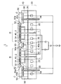
(第1の実施の形態)
図3は第1実施形態の静電チャックを示す断面図、図4は第1実施形態の静電チャックを示す平面図である。
(First embodiment)
FIG. 3 is a sectional view showing the electrostatic chuck of the first embodiment, and FIG. 4 is a plan view showing the electrostatic chuck of the first embodiment.
図3に示すように、第1実施形態の静電チャック1は、ベースプレート20と、ベースプレート20の上にシリコーン樹脂などの接着剤26で接着されたチャック機能部10とを備えている。
As shown in FIG. 3, the
ベースプレート20は、例えばアルミニウムなどの金属から形成され、内部に冷却機構として冷却水路22が設けられている。チャック機能部10は、例えばアルミナなどのセラミックスから形成され、表面にウェハ(被吸着物)が載置される複数のチャック領域Rを備えている。
The
各チャック領域Rにおいて、表面に、伝熱用ガスを供給するためのガス孔30とそれに連通して水平方向に延在する凹部32とが設けられ、凹部32の中に多数の凸部34が島状に配置されている。静電チャック1の各チャック領域Rの表面の多数の凸部34上にウェハ2が接触して載置される。
In each chuck region R, the surface is provided with a
このように、静電チャック1の各チャック領域Rの表面は、ガス孔30に連通する凹部32と多数の凸部34とが設けられてエンボス形状(凹凸形状)になっている。これにより、伝熱用ガスがガス孔30及び凹部32を通ってウェハ2の裏面全体に均一に供給されるようになっている。
As described above, the surface of each chuck region R of the
静電チャック1の各チャック領域Rの内部には、電圧を印加してウェハ2を吸着するための電極40がそれぞれ設けられている。電極40は、好適には、タングステン(W)などの高融点金属から形成される。
In each chuck region R of the
また、静電チャック1のチャック機能部10は、各チャック領域Rの外側領域に設けられた凹面部Cを備えている。凹面部Cは、チャック領域Rを除いてそれらの間の領域から周縁領域までつながって形成されている。凹面部Cの底面は、チャック機能部10の上面より低い位置に配置されている。
Further, the
そして、静電チャック1の各チャック領域Rに対応する部分に開口部50aがそれぞれ設けられた一体型のトレイ50が静電チャック1の凹面部Cに配置されている。トレイ50の開口部50aの各側壁において、厚み方向の下部には内側に突き出るリング状の突出部52がそれぞれ設けられている。
An
トレイ50は、アルミナ(Al2O3)、窒化アルミニウム(AlN)、シリコン窒化物(SiN)、シリコン炭化物(SiC)、又はアルミニウム(Al)などの金属などから形成される。
The
静電チャック1の周縁部にはトレイ50を上下に移動させるための複数のリフトピン54がリング状に配置されている。
A plurality of lift pins 54 for moving the
また、静電チャック1の外周部には、プラズマを静電チャック1内に封じ込めるための石英からなるフォーカスリング56が設けられている。
A
そして、静電チャック1のベースプレート20の冷却水路22に冷却水などの冷媒を流すことにより、各チャック領域Rが冷却される。
And each chuck | zipper area | region R is cooled by flowing refrigerant | coolants, such as a cooling water, into the cooling
さらに、本実施形態の静電チャック1では、ウェハ2ばかりではなくトレイ50を十分に冷却できるように、トレイ50が配置された凹面部Cの下のチャック機能部10の内部に、電圧を印加してトレイ50を吸着するための電極40aが設けられている。
Further, in the
電極40,40aは、1つの電極からなる単極方式であってもよいし、渦巻型やくし歯型などの双電極方式を採用し、双電極にプラス(+)及びマイナス(−)の電圧をそれぞれ印加するようにしてもよい。
The
図3の例では、各チャック領域Rのウェハ2用の一方の電極40にプラス(+)の電圧が印加され、ウェハ2用の他方の電極40にマイナス(−)の電圧が印加される。また、トレイ50用の電極40aには、プラス(+)の電圧が印加される。
In the example of FIG. 3, a plus (+) voltage is applied to one
このようにして、静電チャック1の電極40,40aに所定の電圧を印加すると静電引力によってウェハ2が静電チャック1に吸着する。また同時に、トレイ50が静電チャック1に吸着する。
In this way, when a predetermined voltage is applied to the
図4には、本実施形態の静電チャックを平面からみた様子が示されている。図4の例では、静電チャック1にはチャック領域Rが7つ設けられており、各チャック領域Rの上にウェハ2が載置されている。そして、複数のチャック領域Rを除く斜線ハッチング部にトレイ50が配置されている。
FIG. 4 shows a state in which the electrostatic chuck of the present embodiment is viewed from the plane. In the example of FIG. 4, seven chuck regions R are provided in the
トレイ50が配置された領域がチャック機能部10の凹面部Cとなっている。斜線ハッチング部の下の領域にトレイ50用の電極40a(図3)が設けられている。また、静電チャック1の周縁部に4つのリフトピン54が配置されており、静電チャック1の外周部にフォーカスリング56が備えられている。
A region where the
静電チャック1がドライエッチング装置に装着される場合は、チャンバ内にプラズマが生成されて静電チャック1に載置された複数のウェハ2が冷却された状態で同時にエッチングされる。
When the
図5に示すように、エッチングが終了すると、リフトピン54が上側に移動することでトレイ50が上側に移動し、各ウェハ2の周縁部がトレイ50の突出部52上に乗って上側に持ち上げられる。さらに、アーム(不図示)によって、ウェハ2が搭載されたトレイ50がチャンバから外部に搬送される。
As shown in FIG. 5, when etching is completed, the lift pins 54 move upward to move the
前述した図3の状態でウェハ2がエッチングされる際に、トレイ50もプラズマに晒されるが、トレイ50の下の静電チャック1には、トレイ50用の電極40aが存在するため、トレイ50は静電チャック1に十分に吸着した状態となる。
When the
従って、ウェハ2と同様に、プラズマからトレイ50にかかる熱は静電チャック1から外部に放熱されて十分に冷却される。これにより、エッチング処理中にウェハ2の周縁部の温度が高くなることが回避され、各ウェハ2内において温度の均一性が確保される。
Therefore, similarly to the
その結果、各ウェハ2内でエッチングレートやレジスト又は下地との選択比のばらつきが抑えられ、ウェハ2内のエッチング処理の歩留りを向上させることができる。
As a result, the variation in the etching rate and the selectivity with respect to the resist or the base in each
また、トレイ50が静電チャック1で十分に冷却されるため、トレイ50の温度はエッチング処理の直後においても100℃以下に抑えられる。このため、トレイ50が冷却するまで待つ必要がなく、エッチング処理が完了した後に直ちにアームでトレイ50を搬送することができる。
Further, since the
これにより、エッチング処理のスループット(単位時間あたりのウェハ処理能力)を向上させることができ、生産効率の向上に寄与することができる。 Thereby, the throughput of the etching process (wafer processing capacity per unit time) can be improved, which can contribute to the improvement of production efficiency.
しかも、アームが熱膨張するおそれもなくなるので、信頼性よくアームでトレイ50を搬送することができる。
In addition, since there is no possibility that the arm is thermally expanded, the
なお、前述した静電チャック1は、ベースプレート20内に冷却水路22が設けられて、静電チャック1自体が冷却機構を備えているが、静電チャックは必ずしも冷却機構を備えていなくてもよい。
In the
静電チャックが冷却機構を備えていない場合は、静電チャックが取り付けられる各種製造装置の支持台に冷却機構が設けられおり、その支持台の上に静電チャックが取り付けられて冷却される。以下に説明する第2、第3実施形態においても同様である。 When the electrostatic chuck does not include a cooling mechanism, a cooling mechanism is provided on a support base of various manufacturing apparatuses to which the electrostatic chuck is attached, and the electrostatic chuck is attached on the support base to be cooled. The same applies to the second and third embodiments described below.
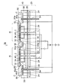
(第2の実施の形態)
図6は第2実施形態の静電チャックを示す断面図である。
(Second Embodiment)
FIG. 6 is a cross-sectional view showing the electrostatic chuck of the second embodiment.
前述した第1実施形態の図3の静電チャック1では、トレイ50と静電チャック1との間に伝熱用ガスを供給しない構造になっている。第2実施形態の特徴は、トレイと静電チャックとの間にも伝熱用ガスを供給して冷却効率を向上させることにある。図6では、第1実施形態と同一要素については同一符号を付してその詳しい説明を省略する。
In the
図6に示すように、第2実施形態の静電チャック1aでは、トレイ50が配置される凹面部Cの表面にも、伝熱用ガスを供給するためのガス孔30aとそれに連通する凹部32aとが設けられている。凹面部Cのガス孔30aはチャック領域Rのガス孔30につながる分岐ラインとして設けられる。
As shown in FIG. 6, in the
ガス孔30,30aを含むガス経路Lからガス孔30,30aに連通する凹部32,32aにヘリウムガスなどの伝熱用ガスを供給することにより、ウェハ2及びトレイ50の各背面に伝熱用ガスをそれぞれ同時に流すことができる。
By supplying heat transfer gas such as helium gas from the gas path L including the gas holes 30 and 30a to the
これにより、ウェハ2と同様に、プラズマから吸収するトレイ50の熱を静電チャック1a側に伝熱用ガスを介して効率よく逃がして冷却することができる。従って、微細加工を達成するために高密度プラズマを使用する場合であっても、トレイ50を十分に冷却することができる。
Thereby, similarly to the
(第3の実施の形態)
図7は第3実施形態の静電チャックを示す断面図である。図7では、第1実施形態と同一要素については同一符号を付してその詳しい説明を省略する。
(Third embodiment)
FIG. 7 is a sectional view showing an electrostatic chuck according to the third embodiment. In FIG. 7, the same elements as those in the first embodiment are denoted by the same reference numerals, and detailed description thereof is omitted.
図7に示す静電チャック1bのように、ウェハ2に伝熱用ガスを供給するガス孔30を含むガス経路L1と、トレイ50に伝熱用ガスを供給するガス孔30aを含むガス経路L2とを分離し、別の独立したラインとしてもよい。
As in the
このようにすることにより、ウェハ2とトレイ50との間で伝熱用ガスの流量やガス圧力を独立して調整することができるので、ウェハ2とトレイ50との間で冷却効率を変えることができる。例えば、エッチング特性や搬送の安定化などの都合で、ウェハ2よりトレイ50を積極的に冷却する必要がある場合などに容易に対応することができる。
In this way, the flow rate and gas pressure of the heat transfer gas can be adjusted independently between the
(第4の実施の形態)
前述した第1〜第3実施形態では、ウェハを冷却するタイプの静電チャックについて説明しており、その場合は伝熱用ガスが冷却用ガスとして機能する。図8に示すように、ベースプレート20の内部に、冷却水路22の代わりに加熱機構としてヒータ電極24を設けることにより、ウェハを加熱するタイプの静電チャック1cとしてもよい。
(Fourth embodiment)
In the first to third embodiments described above, the electrostatic chuck of the type that cools the wafer is described. In this case, the heat transfer gas functions as the cooling gas. As shown in FIG. 8, an electrostatic chuck 1 c that heats the wafer may be provided by providing a
この場合は、伝熱用ガスが加熱用ガスとして機能する。電源(不図示)から電圧をヒータ電極24に印加することにより、ヒータ電極24から熱が発生し、ウェハ2やトレイ50が所定の温度に加熱される。ウェハを加熱するタイプの静電チャック1cは、スパッタ装置やプラズマCVD装置などの半導体・液晶製造装置に適用される。
In this case, the heat transfer gas functions as a heating gas. By applying a voltage from a power source (not shown) to the
図8において、ベースプレート20の内部に冷却水路22の代わりにヒータ電極24を設けること以外は、第1実施形態の図3の静電チャック1と同一である。
8 is the same as the
ウェハを加熱するタイプの静電チャック1cとする場合は、ウェハ2と同様にトレイ50も静電チャック1cに吸着するため、ウェハ2とその周辺のトレイ50とが同一の温度に加熱される。従って、ウェハ2を加熱する場合であってもウェハ2内の温度の均一性を向上させることができ、各種のプロセス処理の信頼性を向上させることができる。
When the electrostatic chuck 1c of the type that heats the wafer is used, the
なお、静電チャック1cにヒータ電極24が設けられておらず、静電チャック1cが取り付けられる各種製造装置の支持台に加熱機構が設けられて静電チャックが加熱されるようにしてもよい。
The electrostatic chuck 1c is not provided with the
また、ウェハを100℃以上に加熱する高温型の静電チャックとする場合は、搬送トラブルを回避するために、トレイ50を搬送するアームとして加熱温度に対して十分な耐熱性を有する特別なアームを使用することが好ましい。
When a high-temperature electrostatic chuck that heats the wafer to 100 ° C. or higher is used, a special arm having sufficient heat resistance against the heating temperature as an arm for transporting the
(半導体・液晶製造装置)
次に、実施形態の静電チャックを備えた半導体・液晶製造装置について説明する。本実施形態の静電チャック1,1a,1b,1cは、半導体装置や液晶表示装置の製造プロセスで使用される各種の半導体・液晶製造装置に適用することができる。
(Semiconductor / LCD manufacturing equipment)
Next, a semiconductor / liquid crystal manufacturing apparatus including the electrostatic chuck according to the embodiment will be described. The
以下の説明では、第1実施形態の冷却される静電チャック1を備えたドライエッチング装置を例に挙げて説明する。
In the following description, the dry etching apparatus including the cooled
図9は実施形態のドライエッチング装置を示す断面図である。図9に示すように、ドライエッチング装置5として平行平板型RIE装置が例示されている。ドライエッチング装置5はチャンバ60を備え、チャンバ60の下側に下部電極70が配置されている。
FIG. 9 is a cross-sectional view showing the dry etching apparatus of the embodiment. As shown in FIG. 9, a parallel plate RIE apparatus is illustrated as the
下部電極70の表面側には前述した第1実施形態の静電チャック1が取り付けられており、静電チャック1には複数のウェハ2(被吸着物)が載置される。
The
下部電極70及び静電チャック1にはRF電力を印加するための高周波電源74が接続されている。高周波電源74にはRF電力の出力のマッチングをとるためのRFマッチャ(不図示)が接続されている。
A high
チャンバ60の上側には下部電極70の対向電極となる上部電極80が配置されており、上部電極80は接地されている。上部電極80にはガス導入管82が連結されており、所定のエッチングガスがチャンバ60内に導入される。
An
チャンバ60の下部には排気管76が接続され、排気管76の末端には真空ポンプが取り付けられている。これにより、エッチングにより生成した反応生成物などが排気管76を通して外部(排ガス処理装置)に排気されるようになっている。
An
チャンバ60の近傍の排気管76にはAPCバルブ78(自動圧力コントロールバルブ)が設けられており、チャンバ60内が設定圧力になるようにAPCバルブ78の開度が自動調整される。
An
本実施形態のドライエッチング装置5では、ガス導入管82から所定のエッチングガスがチャンバ60に導入され、チャンバ60内がAPCバルブ78の機能によって所定の圧力に設定される。そして、高周波電源74から静電チャック1(下部電極70)にRF電力が印加されることにより、チャンバ60内にプラズマが生成される。
In the
静電チャック1にRF電力を印加することにより静電チャック1側に負のセルフバイアスが形成され、その結果プラズマ中の正イオンが静電チャック1側に加速される。これに基づいて、ウェハ2に形成された被エッチング層が異方性エッチングされる。
By applying RF power to the
ウェハ2としては、LEDを製造する場合は、サファイヤ基板、シリコン炭化物(SiC)基板、窒化ガリウム(GaN)基板などが使用される。そして、ウェハ2上に形成された各種の薄膜がレジストをマスクにしてエッチングされる。プロセスガスとしては、フッ素系ガスや塩素系ガスが使用される。
As the
前述したように、本実施形態の静電チャック1(図3など)では、トレイ50の下の静電チャック1に電極40aが設けられており、トレイ50を静電チャック1に吸着させることができる。これにより、ウェハ2と同様にトレイ50も十分に冷却される。
As described above, in the
従って、トレイ50の温度上昇によってウェハ2内で温度がばらついたり、トレイ50を搬送するアームが熱膨張して搬送トラブルが発生することが回避される。
Accordingly, it is possible to avoid the occurrence of a conveyance trouble due to the temperature variation in the
このため、ウェハ2内で被エッチング層のエッチングレート、レジスト及び下地層との選択比などの変動が抑制される。これにより、ウェハ2内においてエッチング後のパターンの幅などのばらつきが抑えられ、ウェハ2内のエッチング処理の歩留りを向上させることができる。
For this reason, fluctuations in the etching rate of the layer to be etched, the selection ratio between the resist and the underlayer, and the like in the
また、微細加工を達成するために高密度プラズマを使用する場合であっても、トレイ50の温度上昇を抑止できるので、安定したエッチング特性を得ることができる。
Further, even when high-density plasma is used to achieve microfabrication, the temperature rise of the
図9では、本実施形態の静電チャック1を平行平板型のドライエッチング装置に適用する形態を例示したが、誘導結合型(ICP)などのドライエッチング装置に適用してもよい。
Although FIG. 9 illustrates an example in which the
1,1a,1b,1c…静電チャック、2…ウェハ、5…ドライエッチング装置、10…チャック機能部、20…ベースプレート、22…冷却水路、24…ヒータ電極、26…接着剤、30,30a…ガス孔、32,32a…凹部、34…凸部、40,40a…電極、50…トレイ、50a…開口部、52…突出部、54…リフトピン、56…フォーカスリング、60…チャンバ、70…下部電極、74…高周波電源、76…排気管、78…APCバルブ、80…上部電極、82…ガス導入管、C…凹面部、L,L1,L2…ガス経路、R…チャック領域。
DESCRIPTION OF
Claims (6)
前記チャック領域に対応する前記チャック機能部の内部と、凹面部に対応する前記チャック機能部の内部とにそれぞれ配置された電極と、
前記チャック領域及び前記凹面部の各表面にそれぞれ設けられ、伝熱用ガスが供給されるガス孔と前記ガス孔に連通する凹部と
を有し、
前記チャック領域の表面に設けられたガス孔を含むガス経路と、前記凹面部の表面に設けられたガス孔を含むガス経路とは、独立した別の経路になっており、
前記チャック領域と前記凹面部との間で、冷却効率が変わるように、前記伝熱用ガスの流量及びガス圧力を独立して調整することを含み、
前記被吸着物が載置される前記チャック領域よりも前記トレイが配置される前記凹面部を積極的に冷却することを特徴とする静電チャック。 A plurality of chuck regions adsorbate is placed, the al provided outside the region of the chuck regions are, chuck function of the entire lower surface of the tray for conveying the adsorbate has a concave portion disposed And
Electrodes disposed respectively inside the chuck function part corresponding to the chuck region and inside the chuck function part corresponding to the concave surface part,
Provided on each surface of the chuck region and the concave surface portion, each having a gas hole to which a heat transfer gas is supplied and a concave portion communicating with the gas hole;
The gas path including the gas holes provided on the surface of the chuck region and the gas path including the gas holes provided on the surface of the concave portion are separate and independent paths.
Independently adjusting the flow rate and gas pressure of the heat transfer gas so that the cooling efficiency changes between the chuck region and the concave surface portion,
The electrostatic chuck characterized in that the concave surface portion where the tray is disposed is more actively cooled than the chuck region where the object to be attracted is placed .
前記チャンバに取り付けられた静電チャックと、
被吸着物を搬送するためのトレイとを有し、
前記静電チャックは、
前記被吸着物が載置される複数のチャック領域と、前記チャック領域の外側領域に設けられた凹面部とを備えたチャック機能部と、
前記チャック領域に対応する前記チャック機能部の内部と、凹面部に対応する前記チャック機能部の内部とにそれぞれ配置された電極と、
前記チャック領域及び前記凹面部の各表面にそれぞれ設けられ、伝熱用ガスが供給されるガス孔と前記ガス孔に連通する凹部と
を有し、
前記チャック領域の表面に設けられたガス孔を含むガス経路と、前記凹面部の表面に設けられたガス孔を含むガス経路とは、独立した別の経路になっており、
前記チャック領域と前記凹面部との間で、冷却効率が変わるように、前記伝熱用ガスの流量及びガス圧力が独立して調整され、
前記トレイは、
前記チャック領域に対応する部分に開口部を備え、前記トレイの下面全体が前記静電チャックの凹面部に配置され、
前記トレイはアームによって搬送され、
前記トレイの搬送の安定化のため、前記被吸着物よりも前記トレイを積極的に冷却することを特徴とする半導体・液晶製造装置。 A chamber;
An electrostatic chuck attached to the chamber;
A tray for transporting the object to be adsorbed,
The electrostatic chuck is
A chuck function unit including a plurality of chuck regions on which the object to be adsorbed is placed, and a concave portion provided in an outer region of the chuck region;
Electrodes disposed respectively inside the chuck function part corresponding to the chuck region and inside the chuck function part corresponding to the concave surface part,
Provided on each surface of the chuck region and the concave surface portion, each having a gas hole to which a heat transfer gas is supplied and a concave portion communicating with the gas hole;
The gas path including the gas holes provided on the surface of the chuck region and the gas path including the gas holes provided on the surface of the concave portion are separate and independent paths.
The flow rate and gas pressure of the heat transfer gas are independently adjusted so that the cooling efficiency changes between the chuck region and the concave surface portion,
The tray
An opening is provided in a portion corresponding to the chuck region, and the entire lower surface of the tray is disposed in a concave portion of the electrostatic chuck ,
The tray is conveyed by an arm,
A semiconductor / liquid crystal manufacturing apparatus, wherein the tray is more actively cooled than the adsorbed object in order to stabilize conveyance of the tray .
前記半導体・液晶製造装置は、ドライエッチング装置であることを特徴とする請求項4に記載の半導体・液晶製造装置。 The electrostatic chuck further includes a base plate disposed under the chuck function unit and provided with a cooling mechanism,
The semiconductor / liquid crystal manufacturing apparatus according to claim 4, wherein the semiconductor / liquid crystal manufacturing apparatus is a dry etching apparatus.
前記チャック領域に対応する前記チャック機能部の内部に配置された前記電極と、前記凹面部に対応する前記チャック機能部の内部に配置された前記電極とは、独立して設けられていることを特徴とする請求項4又は5に記載の半導体・液晶製造装置。 In the electrostatic chuck,
The electrode arranged inside the chuck function part corresponding to the chuck region and the electrode arranged inside the chuck function part corresponding to the concave surface part are provided independently. The semiconductor / liquid crystal manufacturing apparatus according to claim 4 or 5, characterized in that:
Priority Applications (5)
| Application Number | Priority Date | Filing Date | Title |
|---|---|---|---|
| JP2011184285A JP6285620B2 (en) | 2011-08-26 | 2011-08-26 | Electrostatic chuck and semiconductor / liquid crystal manufacturing equipment |
| TW101124751A TWI563583B (en) | 2011-08-26 | 2012-07-10 | Electrostatic chuck and semiconductor/liquid crystal manufacturing equipment |
| KR1020120075809A KR102056723B1 (en) | 2011-08-26 | 2012-07-12 | Electrostatic chuck and semiconductor/liquid crystal manufacturing equipment |
| US13/547,316 US11037811B2 (en) | 2011-08-26 | 2012-07-12 | Electrostatic chuck and semiconductor/liquid crystal manufacturing equipment |
| CN201210273478.2A CN102956533B (en) | 2011-08-26 | 2012-08-02 | The manufacture device of electrostatic chuck and semiconductor device or liquid crystal display device |
Applications Claiming Priority (1)
| Application Number | Priority Date | Filing Date | Title |
|---|---|---|---|
| JP2011184285A JP6285620B2 (en) | 2011-08-26 | 2011-08-26 | Electrostatic chuck and semiconductor / liquid crystal manufacturing equipment |
Publications (3)
| Publication Number | Publication Date |
|---|---|
| JP2013045989A JP2013045989A (en) | 2013-03-04 |
| JP2013045989A5 JP2013045989A5 (en) | 2014-07-31 |
| JP6285620B2 true JP6285620B2 (en) | 2018-02-28 |
Family
ID=47741925
Family Applications (1)
| Application Number | Title | Priority Date | Filing Date |
|---|---|---|---|
| JP2011184285A Active JP6285620B2 (en) | 2011-08-26 | 2011-08-26 | Electrostatic chuck and semiconductor / liquid crystal manufacturing equipment |
Country Status (5)
| Country | Link |
|---|---|
| US (1) | US11037811B2 (en) |
| JP (1) | JP6285620B2 (en) |
| KR (1) | KR102056723B1 (en) |
| CN (1) | CN102956533B (en) |
| TW (1) | TWI563583B (en) |
Families Citing this family (26)
| Publication number | Priority date | Publication date | Assignee | Title |
|---|---|---|---|---|
| US9668373B2 (en) * | 2013-03-15 | 2017-05-30 | Applied Materials, Inc. | Substrate support chuck cooling for deposition chamber |
| CN104134624B (en) * | 2013-05-02 | 2017-03-29 | 北京北方微电子基地设备工艺研究中心有限责任公司 | Pallet and plasma processing device |
| JP6348321B2 (en) * | 2013-05-17 | 2018-06-27 | キヤノンアネルバ株式会社 | Etching device |
| CN104465453B (en) * | 2013-09-20 | 2018-10-30 | 住友电气工业株式会社 | The wafer heater of plasma CVD equipment |
| JP5938716B2 (en) * | 2013-11-01 | 2016-06-22 | パナソニックIpマネジメント株式会社 | Plasma processing apparatus and plasma processing method |
| CN104752301B (en) * | 2013-12-31 | 2018-05-25 | 北京北方华创微电子装备有限公司 | A kind of electrostatic chuck and chamber |
| CN105280518B (en) * | 2014-05-30 | 2020-09-08 | 盛美半导体设备(上海)股份有限公司 | Heat treatment device for semiconductor substrate |
| CN105448631B (en) * | 2014-06-12 | 2017-07-25 | 中微半导体设备(上海)有限公司 | A kind of substrate mounting platform and a kind of plasma treatment appts and its operation method |
| JP6377975B2 (en) * | 2014-06-23 | 2018-08-22 | 新光電気工業株式会社 | Substrate fixing device |
| US10030303B2 (en) * | 2014-12-19 | 2018-07-24 | Sunpower Corporation | Sputter tool |
| US9633886B2 (en) * | 2015-04-16 | 2017-04-25 | Varian Semiconductor Equipment Associates, Inc. | Hybrid thermal electrostatic clamp |
| CN107113921B (en) * | 2015-08-20 | 2020-09-11 | 日本碍子株式会社 | Electrostatic chuck heater |
| CN105551926B (en) * | 2015-12-11 | 2017-10-03 | 中国电子科技集团公司第四十八研究所 | A kind of use pedestal cools down the rotational workpieces platform of rotational workpieces |
| WO2017195672A1 (en) * | 2016-05-09 | 2017-11-16 | 株式会社 アルバック | Electrostatic chuck and plasma treatment device |
| JP6858035B2 (en) | 2017-02-27 | 2021-04-14 | 新光電気工業株式会社 | Board fixtures and board fixing devices |
| CN110678971B (en) * | 2017-06-16 | 2024-04-16 | 周星工程股份有限公司 | Substrate processing apparatus and rotary electrical connector for vacuum |
| JP6518024B1 (en) * | 2017-10-30 | 2019-05-22 | 日本碍子株式会社 | Electrostatic chuck and manufacturing method thereof |
| JP6894000B2 (en) | 2017-11-06 | 2021-06-23 | 日本碍子株式会社 | Electrostatic chuck assembly and electrostatic chuck |
| JP6965776B2 (en) * | 2018-02-08 | 2021-11-10 | トヨタ自動車株式会社 | Electrostatic suction transfer device and its method |
| WO2019187785A1 (en) * | 2018-03-26 | 2019-10-03 | 日本碍子株式会社 | Electrostatic chuck heater |
| CN113711343A (en) * | 2019-02-05 | 2021-11-26 | 应用材料公司 | Substrate support for adsorbing a mask for a deposition process |
| US20200286717A1 (en) * | 2019-03-08 | 2020-09-10 | Applied Materials, Inc. | Electrostatic chuck for high bias radio frequency (rf) power application in a plasma processing chamber |
| JP6918042B2 (en) * | 2019-03-26 | 2021-08-11 | 日本碍子株式会社 | Wafer mounting device |
| TW202137326A (en) * | 2020-03-03 | 2021-10-01 | 日商東京威力科創股份有限公司 | Substrate support, plasma processing system, and method of placing annular member |
| CN111900118B (en) * | 2020-06-19 | 2023-04-07 | 中国科学院微电子研究所 | Wafer transfer mechanism, semiconductor manufacturing equipment and wafer transfer method |
| US20240266200A1 (en) * | 2023-02-08 | 2024-08-08 | Applied Materials, Inc. | Electrostatic Chuck |
Family Cites Families (12)
| Publication number | Priority date | Publication date | Assignee | Title |
|---|---|---|---|---|
| JP3090339B2 (en) * | 1990-03-19 | 2000-09-18 | 株式会社東芝 | Vapor growth apparatus and method |
| JP3297288B2 (en) * | 1996-02-13 | 2002-07-02 | 株式会社東芝 | Apparatus and method for manufacturing semiconductor device |
| US6344105B1 (en) * | 1999-06-30 | 2002-02-05 | Lam Research Corporation | Techniques for improving etch rate uniformity |
| US6646233B2 (en) * | 2002-03-05 | 2003-11-11 | Hitachi High-Technologies Corporation | Wafer stage for wafer processing apparatus and wafer processing method |
| JP4547182B2 (en) * | 2003-04-24 | 2010-09-22 | 東京エレクトロン株式会社 | Plasma processing equipment |
| US20040261946A1 (en) * | 2003-04-24 | 2004-12-30 | Tokyo Electron Limited | Plasma processing apparatus, focus ring, and susceptor |
| JP2006319043A (en) | 2005-05-11 | 2006-11-24 | Hitachi High-Technologies Corp | Plasma processor |
| KR101153118B1 (en) * | 2005-10-12 | 2012-06-07 | 파나소닉 주식회사 | Plasma processing apparatus and plasma processing method |
| US7651571B2 (en) * | 2005-12-22 | 2010-01-26 | Kyocera Corporation | Susceptor |
| KR20110137775A (en) * | 2009-03-26 | 2011-12-23 | 파나소닉 주식회사 | Plasma processing apparatus and plasma processing method |
| JP2010232250A (en) * | 2009-03-26 | 2010-10-14 | Panasonic Corp | Plasma treating apparatus |
| JP2011114178A (en) * | 2009-11-27 | 2011-06-09 | Samco Inc | Plasma processing device and plasma processing method |
-
2011
- 2011-08-26 JP JP2011184285A patent/JP6285620B2/en active Active
-
2012
- 2012-07-10 TW TW101124751A patent/TWI563583B/en active
- 2012-07-12 US US13/547,316 patent/US11037811B2/en active Active
- 2012-07-12 KR KR1020120075809A patent/KR102056723B1/en active IP Right Grant
- 2012-08-02 CN CN201210273478.2A patent/CN102956533B/en active Active
Also Published As
| Publication number | Publication date |
|---|---|
| TWI563583B (en) | 2016-12-21 |
| KR102056723B1 (en) | 2019-12-17 |
| US20130048217A1 (en) | 2013-02-28 |
| CN102956533B (en) | 2018-04-06 |
| TW201310564A (en) | 2013-03-01 |
| JP2013045989A (en) | 2013-03-04 |
| KR20130023062A (en) | 2013-03-07 |
| CN102956533A (en) | 2013-03-06 |
| US11037811B2 (en) | 2021-06-15 |
Similar Documents
| Publication | Publication Date | Title |
|---|---|---|
| JP6285620B2 (en) | Electrostatic chuck and semiconductor / liquid crystal manufacturing equipment | |
| US11355323B2 (en) | Plasma processing apparatus and method therefor | |
| JP6024921B2 (en) | Plasma processing apparatus and plasma processing method | |
| JP4935143B2 (en) | Mounting table and vacuum processing apparatus | |
| JP6268095B2 (en) | Thermal management of edge rings in semiconductor processing. | |
| US20120273135A1 (en) | Electrode unit, substrate processing apparatus, and temperature control method for electrode unit | |
| KR102604063B1 (en) | Electrostatic chuck assembly and substrate treating apparatus including the assembly | |
| JP4878109B2 (en) | Substrate transfer system and substrate transfer method | |
| JP2011114178A (en) | Plasma processing device and plasma processing method | |
| JP5243465B2 (en) | Plasma processing equipment | |
| TW201230242A (en) | Substrate stage, substrate processing apparatus and substrate processing system | |
| JP7209515B2 (en) | Substrate holding mechanism and deposition equipment | |
| TW201926538A (en) | Substrate table | |
| JP5866595B2 (en) | Tray for plasma processing apparatus and plasma processing apparatus | |
| TW201907507A (en) | Temperature adjustment substrate holder for substrate processing system | |
| KR20210157876A (en) | Plasma processing system, plasma processing apparatus, and method for replacing edge ring | |
| US11605551B2 (en) | Chuck assembly, semiconductor device fabricating apparatus including the same, and method of fabricating semiconductor device | |
| US11104996B2 (en) | Heating stage and apparatus having the same | |
| JP2024098708A (en) | Plasma processing apparatus | |
| CN116153835A (en) | Substrate support and substrate processing apparatus | |
| JP2013187449A (en) | Etching device |
Legal Events
| Date | Code | Title | Description |
|---|---|---|---|
| A521 | Written amendment |
Free format text: JAPANESE INTERMEDIATE CODE: A523 Effective date: 20140611 |
|
| A621 | Written request for application examination |
Free format text: JAPANESE INTERMEDIATE CODE: A621 Effective date: 20140611 |
|
| A977 | Report on retrieval |
Free format text: JAPANESE INTERMEDIATE CODE: A971007 Effective date: 20150311 |
|
| A131 | Notification of reasons for refusal |
Free format text: JAPANESE INTERMEDIATE CODE: A131 Effective date: 20150407 |
|
| A521 | Written amendment |
Free format text: JAPANESE INTERMEDIATE CODE: A523 Effective date: 20150601 |
|
| A02 | Decision of refusal |
Free format text: JAPANESE INTERMEDIATE CODE: A02 Effective date: 20160301 |
|
| A521 | Written amendment |
Free format text: JAPANESE INTERMEDIATE CODE: A523 Effective date: 20160526 |
|
| A911 | Transfer to examiner for re-examination before appeal (zenchi) |
Free format text: JAPANESE INTERMEDIATE CODE: A911 Effective date: 20160607 |
|
| A912 | Re-examination (zenchi) completed and case transferred to appeal board |
Free format text: JAPANESE INTERMEDIATE CODE: A912 Effective date: 20160708 |
|
| A521 | Written amendment |
Free format text: JAPANESE INTERMEDIATE CODE: A523 Effective date: 20170913 |
|
| A61 | First payment of annual fees (during grant procedure) |
Free format text: JAPANESE INTERMEDIATE CODE: A61 Effective date: 20180202 |
|
| R150 | Certificate of patent or registration of utility model |
Ref document number: 6285620 Country of ref document: JP Free format text: JAPANESE INTERMEDIATE CODE: R150 |