JP6282012B2 - LIGHTING POWER DEVICE AND LIGHTING POWER SYSTEM - Google Patents
LIGHTING POWER DEVICE AND LIGHTING POWER SYSTEM Download PDFInfo
- Publication number
- JP6282012B2 JP6282012B2 JP2014210051A JP2014210051A JP6282012B2 JP 6282012 B2 JP6282012 B2 JP 6282012B2 JP 2014210051 A JP2014210051 A JP 2014210051A JP 2014210051 A JP2014210051 A JP 2014210051A JP 6282012 B2 JP6282012 B2 JP 6282012B2
- Authority
- JP
- Japan
- Prior art keywords
- voltage
- power supply
- input
- switch
- discharge path
- Prior art date
- Legal status (The legal status is an assumption and is not a legal conclusion. Google has not performed a legal analysis and makes no representation as to the accuracy of the status listed.)
- Active
Links
Images
Classifications
-
- Y—GENERAL TAGGING OF NEW TECHNOLOGICAL DEVELOPMENTS; GENERAL TAGGING OF CROSS-SECTIONAL TECHNOLOGIES SPANNING OVER SEVERAL SECTIONS OF THE IPC; TECHNICAL SUBJECTS COVERED BY FORMER USPC CROSS-REFERENCE ART COLLECTIONS [XRACs] AND DIGESTS
- Y02—TECHNOLOGIES OR APPLICATIONS FOR MITIGATION OR ADAPTATION AGAINST CLIMATE CHANGE
- Y02B—CLIMATE CHANGE MITIGATION TECHNOLOGIES RELATED TO BUILDINGS, e.g. HOUSING, HOUSE APPLIANCES OR RELATED END-USER APPLICATIONS
- Y02B20/00—Energy efficient lighting technologies, e.g. halogen lamps or gas discharge lamps
- Y02B20/40—Control techniques providing energy savings, e.g. smart controller or presence detection
Landscapes
- Circuit Arrangement For Electric Light Sources In General (AREA)
Description
本発明は、調光機能を有する照明用電源装置および当該照明用電源装置を複数備えた照明用電源システムに関する。 The present invention relates to an illumination power supply device having a dimming function and an illumination power supply system including a plurality of the illumination power supply devices.
従来から、調光機能を有する照明用電源装置として、例えば、非特許文献1に記載のものが知られている。図5に示すように、非特許文献1に記載の照明用電源装置11は、整流平滑回路2と、スイッチ手段Q1を含む出力電流生成回路3と、スイッチ手段Q1を制御する制御回路U1と、制御回路U1の電源電圧(VDD電圧)を生成する電源電圧生成回路4とを主に備えており、LED照明装置20に供給する直流出力電流の電流量を予め設定された順序で段階的に切り替えることができる。なお、LED照明装置20は、直列接続された複数(例えば、12個)のLEDを光源として含み、供給される直流出力電流の電流量に応じて光源の明るさが変わる。
Conventionally, as a power supply device for illumination having a dimming function, for example, the one described in Non-Patent
整流平滑回路2は、入力された交流入力電圧を整流するダイオードブリッジDBと、整流後の交流入力電圧を平滑するコンデンサC1、C2とを含んでいる。照明用電源装置11の入力端と整流平滑回路2との間には、ヒューズFが設けられている。
The rectifying /
出力電流生成回路3は、電流路の一端(ドレイン)が整流平滑回路2の出力側に接続されたMOSFETからなるスイッチ手段Q1と、照明用電源装置11のプラス側の出力端とスイッチ手段Q1の電流路の他端(ソース)と間に介装された抵抗R5およびコイルL1(トランスの一次巻線)からなる直列回路と、カソードがスイッチ手段Q1と抵抗R5との接続点に接続され、アノードがグラウンド接続されたダイオードD2と、一端がコイルL1とプラス側の出力端との接続点に接続され、他端がグラウンド接続されたコンデンサC3と、一端がコンデンサC3の一端に接続され、他端が照明用電源装置11のマイナス側の出力端に接続された抵抗R6を含んでいる。
The output
スイッチ手段Q1は、制御回路U1の制御下でスイッチング動作を行う。スイッチ手段Q1のONデューティが大きいほど、照明用電源装置11から出力される直流出力電流の電流量は大きくなる。すなわち、スイッチ手段Q1のONデューティを段階的に切り替えることで、直流出力電流の電流量が段階的に切り替わり、その結果、LED照明装置20の明るさが段階的に切り替わる。
The switch means Q1 performs a switching operation under the control of the control circuit U1. The larger the ON duty of the switch means Q1, the greater the amount of DC output current output from the illumination
電源電圧生成回路4は、一端がフレームグラウンドに接続されたコイルL2(トランスの二次巻線)と、アノードがコイルL2の他端に接続され、カソードが抵抗R8を介して制御回路U1の電源電圧端子(VDD端子)に接続されたダイオードD1と、一端がVDD端子と抵抗R8との接続点に接続されたコンデンサC5とを含んでいる。コンデンサC5は、交流入力電圧が入力状態(ON)のときに充電され、交流入力電圧が非入力状態(OFF)のときに放電して制御回路U1に電源電圧(VDD電圧)を供給する。 The power supply voltage generation circuit 4 includes a coil L2 (secondary winding of the transformer) having one end connected to the frame ground, an anode connected to the other end of the coil L2, and a cathode connected to the power supply of the control circuit U1 via the resistor R8. It includes a diode D1 connected to the voltage terminal (VDD terminal) and a capacitor C5 having one end connected to a connection point between the VDD terminal and the resistor R8. The capacitor C5 is charged when the AC input voltage is in the input state (ON), and is discharged when the AC input voltage is in the non-input state (OFF) to supply the power supply voltage (VDD voltage) to the control circuit U1.
制御回路U1は、ZCD端子と、GND端子と、COMP端子と、CS端子と、DRV端子と、VDD端子とを備えている。ZCD端子は、コイルL2に流れる電流がボトム(最小値)となるタイミングの検出と過電圧保護動作とを行うための端子であり、抵抗R7を介してコイルL2の他端に接続されている。COMP端子は、エラーアンプの端子であり、コンデンサC4を介してフレームグラウンドに接続されている。CS端子は、スイッチ手段Q1のドレイン電流をモニターするための端子であり、スイッチ手段Q1と抵抗R5との接続点に接続されている。DRV端子は、スイッチ手段Q1の制御端子(ゲート)に駆動信号を出力するための端子であり、抵抗R4を介してスイッチ手段Q1のゲートに接続されている。VDD端子は、制御回路U1の電源電圧(VDD電圧)が供給される端子であり、抵抗R1、R2、R3を介して照明用電源装置11の入力端に接続され、かつコンデンサC5と抵抗R8の接続点に接続されている。
The control circuit U1 includes a ZCD terminal, a GND terminal, a COMP terminal, a CS terminal, a DRV terminal, and a VDD terminal. The ZCD terminal is a terminal for detecting the timing when the current flowing through the coil L2 becomes the bottom (minimum value) and the overvoltage protection operation, and is connected to the other end of the coil L2 via the resistor R7. The COMP terminal is an error amplifier terminal, and is connected to the frame ground via a capacitor C4. The CS terminal is a terminal for monitoring the drain current of the switch means Q1, and is connected to the connection point between the switch means Q1 and the resistor R5. The DRV terminal is a terminal for outputting a drive signal to the control terminal (gate) of the switch means Q1, and is connected to the gate of the switch means Q1 via a resistor R4. The VDD terminal is a terminal to which the power supply voltage (VDD voltage) of the control circuit U1 is supplied, is connected to the input terminal of the illumination
制御回路U1は、VDD電圧をモニターし、VDD電圧の電圧値に応じた駆動信号をDRV端子から出力することによりスイッチ手段Q1のONデューティを制御する「調光制御」を行う。 The control circuit U1 performs “dimming control” for controlling the ON duty of the switch means Q1 by monitoring the VDD voltage and outputting a drive signal corresponding to the voltage value of the VDD voltage from the DRV terminal.
図6に、照明用電源装置11における調光制御と直流出力電流の電流量との関係を示す。制御回路U1では、動作電圧V1、スレッシュ電圧V2(例えば、約10.0V)、リセット電圧V3(例えば、約2.5V)が予め設定されており、スイッチ手段Q1のONデューティを切り替える順序(100%→40%→2.5%)も予め設定されている。
FIG. 6 shows the relationship between the dimming control in the illumination
交流入力電圧が非入力状態(OFF)から入力状態(ON)に切り替わると、VDD電圧は、動作電圧V1まで一気に上昇する。VDD電圧が動作電圧V1まで上昇すると、制御回路U1は、スイッチ手段Q1のゲートに駆動信号を出力してスイッチ手段Q1のスイッチング動作を開始させる。 When the AC input voltage is switched from the non-input state (OFF) to the input state (ON), the VDD voltage rises at a stretch to the operating voltage V1. When the VDD voltage rises to the operating voltage V1, the control circuit U1 outputs a drive signal to the gate of the switch means Q1 to start the switching operation of the switch means Q1.
一方、交流入力電圧が入力状態(ON)から非入力状態(OFF)に切り替わると、VDD電圧は、動作電圧V1からスレッシュ電圧V2まで一気に低下する。VDD電圧がスレッシュ電圧V2まで低下すると、制御回路U1がスイッチ手段Q1のスイッチング動作を停止させるので、制御回路U1の消費電流が低下する。その結果、コンデンサC5の放電速度も低下し、VDD電圧の低下が緩やかになる。 On the other hand, when the AC input voltage is switched from the input state (ON) to the non-input state (OFF), the VDD voltage drops from the operating voltage V1 to the threshold voltage V2. When the VDD voltage decreases to the threshold voltage V2, the control circuit U1 stops the switching operation of the switch means Q1, so that the current consumption of the control circuit U1 decreases. As a result, the discharge rate of the capacitor C5 also decreases, and the VDD voltage decreases gradually.
また、制御回路U1は、交流入力電圧が非入力状態(OFF)から入力状態(ON)に切り替わるタイミングに応じて、スイッチ手段Q1のONデューティを変える。 Further, the control circuit U1 changes the ON duty of the switch means Q1 according to the timing at which the AC input voltage is switched from the non-input state (OFF) to the input state (ON).
より詳しくは、VDD電圧がリセット電圧V3に達する前に交流入力電圧が非入力状態(OFF)から入力状態(ON)に切り替わった場合、制御回路U1は、スイッチ手段Q1のONデューティが予め設定された順序(100%→40%→2.5%)で切り替わるように、スイッチ手段Q1のスイッチング動作を制御する。すなわち、制御回路U1は、直前のONデューティが100%のときは40%のONデューティになるように、直前のONデューティが40%のときは2.5%のONデューティになるように、直前のONデューティが2.5%のときは100%のONデューティになるように、スイッチ手段Q1のスイッチング動作を制御する。 More specifically, when the AC input voltage is switched from the non-input state (OFF) to the input state (ON) before the VDD voltage reaches the reset voltage V3, the control circuit U1 sets the ON duty of the switch means Q1 in advance. The switching operation of the switch means Q1 is controlled so as to be switched in the order (100% → 40% → 2.5%). That is, the control circuit U1 has a 40% ON duty when the immediately preceding ON duty is 100%, and a 2.5% ON duty when the immediately preceding ON duty is 40%. When the ON duty is 2.5%, the switching operation of the switch means Q1 is controlled so that the ON duty becomes 100%.
一方、VDD電圧がリセット電圧V3に達した後に交流入力電圧が非入力状態(OFF)から入力状態(ON)に切り替わった場合、制御回路U1は、スイッチ手段Q1のONデューティが上記順序の最初の状態(100%の状態)に切り替わるように、スイッチ手段Q1のスイッチング動作を開始させる。すなわち、制御回路U1は、直前のONデューティが100%または40%であったとしても、100%のONデューティになるように、スイッチ手段Q1のスイッチング動作を制御する。 On the other hand, when the AC input voltage is switched from the non-input state (OFF) to the input state (ON) after the VDD voltage reaches the reset voltage V3, the control circuit U1 determines that the ON duty of the switch means Q1 is the first in the above order. The switching operation of the switch means Q1 is started so as to switch to the state (100% state). That is, the control circuit U1 controls the switching operation of the switch means Q1 so that the ON duty is 100% even if the immediately preceding ON duty is 100% or 40%.
以上のように、照明用電源装置11では、VDD電圧がリセット電圧V3に達する前に交流入力電圧の入力/非入力の切り替えを繰り返すことで、LED照明装置20に供給する直流出力電流の電流量を予め設定された順序で段階的に切り替えることができる。
As described above, in the lighting
ところで、図7に示すように、単一の交流電圧源30に対して複数(N個、Nは3以上の整数)の照明用電源装置11−1〜11−Nを並列に接続した照明用電源システム101の場合、各照明用電源装置11−1〜11−Nに備えられた制御回路U1〜UNのリセット電圧V3は、制御回路U1〜UNによってバラツキが生じることがある。リセット電圧V3にバラツキが生じると、リセット時間(VDD電圧がスレッシュ電圧V2からリセット電圧V3に達するまでの時間)にもバラツキが生じるため、照明用電源システム101では、LED照明装置20−1〜20−Nの中で明るさの異なるものが存在してしまうおそれがあった。なお、各照明用電源装置11−1〜11−NおよびLED照明装置20−1〜20−Nの構成要素については、いずれも図5に示す照明用電源装置11およびLED照明装置20と同様とする。
By the way, as shown in FIG. 7, a plurality of (N, N is an integer of 3 or more) illumination power supply devices 11-1 to 11 -N connected in parallel to a single
例えば、照明用電源装置11−1に備えられた制御回路U1のリセット電圧V3が最も小さく、照明用電源装置11−2に備えられた制御回路U2のリセット電圧V3が最も大きい場合(以下、制御回路U1のリセット電圧V3をV3MINとし、制御回路U2のリセット電圧V3をV3MAXとする。)、図8に示すように、制御回路U1、U2のVDD電圧がリセット電圧V3MAXよりも小さく、かつリセット電圧V3MINよりも大きいときに、交流入力電圧が非入力状態(OFF)から入力状態(ON)に切り替わると、制御回路U1は、スイッチ手段Q1のONデューティが予め設定された順序(40%→2.5%)で切り替わるように、スイッチ手段Q1のスイッチング動作を開始させる一方、制御回路U2は、スイッチ手段Q1のONデューティが上記順序の最初の状態(100%の状態)に切り替わるように、スイッチ手段Q1のスイッチング動作を開始させる。 For example, when the reset voltage V3 of the control circuit U1 provided in the illumination power supply device 11-1 is the lowest and the reset voltage V3 of the control circuit U2 provided in the illumination power supply device 11-2 is the highest (hereinafter referred to as control). The reset voltage V3 of the circuit U1 is set to V3 MIN, and the reset voltage V3 of the control circuit U2 is set to V3 MAX .) As shown in FIG. 8, the VDD voltages of the control circuits U1 and U2 are smaller than the reset voltage V3 MAX . When the AC input voltage is switched from the non-input state (OFF) to the input state (ON) when the reset voltage V3 MIN is greater than the reset voltage V3 MIN , the control circuit U1 determines the order in which the ON duty of the switch means Q1 is set in advance (40 % → 2.5%), the switching means Q1 starts the switching operation, while the control circuit U2 The switching operation of the switch means Q1 is started so that the ON duty of the stage Q1 is switched to the first state (100% state) in the above order.
これにより、LED照明装置20−1にはONデューティ2.5%に相当する直流出力電流が供給されるのに対して(図8(C)参照)、LED照明装置20−2にはONデューティ100%に相当する直流出力電流が供給される(図8(D)参照)。その結果、照明用電源システム101では、LED照明装置20−1とLED照明装置20−2との明るさが異なってしまう。
As a result, a DC output current corresponding to an ON duty of 2.5% is supplied to the LED lighting device 20-1 (see FIG. 8C), whereas an ON duty is supplied to the LED lighting device 20-2. A DC output current corresponding to 100% is supplied (see FIG. 8D). As a result, in the illumination
本発明は上記事情に鑑みてなされたものであって、その課題とするところは、リセット時間のバラツキを解消することが可能な照明用電源装置および照明用電源システムを提供することにある。 This invention is made | formed in view of the said situation, The place made into the subject is providing the power supply device for illumination and the power supply system for illumination which can eliminate the variation in reset time.
上記課題を解決するために、本発明に係る照明用電源装置は、入力電圧の入力状態と入力電圧の非入力状態との繰り返しに応じて、照明装置に供給する出力電流の電流量を予め設定された順序で段階的に切り替える照明用電源装置であって、スイッチング動作により出力電流を生成するスイッチ手段と、入力電圧に応じた電源電圧が供給され、非入力状態から入力状態に切り替わった際、電源電圧の電圧値が予め設定されたリセット電圧よりも大きい場合は出力電流の電流量が上記順序に従って切り替わる一方、電源電圧の電圧値がリセット電圧よりも小さい場合は出力電流の電流量が上記順序の最初の状態に切り替わるように、スイッチ手段を制御する制御回路と、入力状態のときに充電され、かつ非入力状態のときに第1放電経路で放電して制御回路に電源電圧を供給するコンデンサと、入力状態から非入力状態に切り替わった後、第1放電経路での放電により電源電圧がリセット電圧以下になる前に、第1放電経路とは異なる第2放電経路を形成してコンデンサを放電させる放電回路と、を備えたことを特徴とする。 In order to solve the above-described problem, the power supply device for lighting according to the present invention presets the amount of output current supplied to the lighting device in accordance with repetition of the input state of the input voltage and the non-input state of the input voltage. It is a lighting power supply device that switches step by step in the order in which the switching means for generating the output current by switching operation and the power supply voltage corresponding to the input voltage are supplied, and when the non-input state is switched to the input state, When the voltage value of the power supply voltage is larger than the preset reset voltage, the current amount of the output current is switched according to the above order, while when the power supply voltage value is smaller than the reset voltage, the current amount of the output current is the above order. A control circuit for controlling the switching means so as to switch to the first state of the battery, and charging in the input state and discharging in the first discharge path in the non-input state And a capacitor for supplying a power supply voltage to the control circuit, and after switching from the input state to the non-input state, before the power supply voltage becomes lower than the reset voltage due to the discharge in the first discharge path, And a discharge circuit for discharging the capacitor by forming two discharge paths.
この構成によれば、電源電圧がリセット電圧以下になる前に、電源電圧を供給するコンデンサを強制的に放電させることができるので、リセット時間がリセット電圧に左右されることがなくなる。したがって、この構成によれば、リセット時間のバラツキを解消することが可能となる。 According to this configuration, since the capacitor that supplies the power supply voltage can be forcibly discharged before the power supply voltage becomes equal to or lower than the reset voltage, the reset time does not depend on the reset voltage. Therefore, according to this configuration, it is possible to eliminate variations in reset time.
上記照明用電源装置では、放電回路は、照明装置に供給される出力電圧の低下を検出し、出力電圧が所定の閾値よりも小さくなると検出信号を出力する出力電圧検出部と、検出信号が入力されているときに第2放電経路を形成する放電経路形成部と、を含むことが好ましい。 In the illumination power supply device, the discharge circuit detects a decrease in the output voltage supplied to the illumination device, and outputs an output voltage detection unit when the output voltage becomes smaller than a predetermined threshold, and the detection signal is input. And a discharge path forming part that forms a second discharge path when being formed.
上記照明用電源装置では、例えば、出力電圧検出部は、出力電圧が閾値よりも小さくなると非導通状態になる第1スイッチと、第1スイッチが非導通状態になると非導通状態になる第2スイッチと、第2スイッチが非導通状態になると導通状態になる第3スイッチと、第3スイッチが導通状態になると検出信号として光を発する発光素子と、を含み、放電経路形成部は、発光素子の光を受光しているときに第2放電経路を形成する受光素子を含むよう構成できる。 In the illumination power supply device, for example, the output voltage detection unit includes a first switch that becomes non-conductive when the output voltage becomes lower than a threshold value, and a second switch that becomes non-conductive when the first switch becomes non-conductive. And a third switch that is turned on when the second switch is turned off, and a light emitting element that emits light as a detection signal when the third switch is turned on. A light receiving element that forms the second discharge path when receiving light can be included.
上記課題を解決するために、本発明に係る照明用電源システムは、入力端が単一の電圧源に接続され、かつ出力端がそれぞれ別の照明装置に接続される複数の照明用電源装置を含み、複数の照明用電源装置のそれぞれが、電圧源からの入力電圧の入力状態と入力電圧の非入力状態との繰り返しに応じて、出力端に接続された照明装置に供給する出力電流の電流量を予め設定された順序で段階的に切り替える照明用電源システムであって、照明用電源装置は、スイッチング動作により出力電流を生成するスイッチ手段と、入力電圧に応じた電源電圧が供給され、非入力状態から入力状態に切り替わった際、電源電圧の電圧値がリセット電圧よりも大きい場合は出力電流の電流量が上記順序に従って切り替わる一方、電源電圧の電圧値がリセット電圧よりも小さい場合は出力電流の電流量が上記順序の最初の状態に切り替わるように、スイッチ手段を制御する制御回路と、入力状態のときに充電され、かつ非入力状態のときに第1放電経路で放電して制御回路に電源電圧を供給するコンデンサと、第1放電経路とは異なる第2放電経路を形成してコンデンサを放電させる放電回路と、を備え、リセット電圧は、制御回路ごとに予め設定されており、放電回路は、入力状態から非入力状態に切り替わった後、第1放電経路での放電により電源電圧が、制御回路ごとに予め設定されたリセット電圧の最大値以下になる前に、第2放電経路を形成してコンデンサを放電させることを特徴とする。 In order to solve the above-described problems, an illumination power supply system according to the present invention includes a plurality of illumination power supply devices whose input ends are connected to a single voltage source and whose output ends are connected to different illumination devices. Each of the plurality of lighting power supply devices includes a current of an output current supplied to the lighting device connected to the output terminal according to the repetition of the input state of the input voltage from the voltage source and the non-input state of the input voltage. A lighting power supply system that switches the amount step by step in a preset order, wherein the lighting power supply device is supplied with switch means for generating an output current by a switching operation and a power supply voltage corresponding to the input voltage, When switching from the input state to the input state, if the voltage value of the power supply voltage is greater than the reset voltage, the current amount of the output current is switched according to the above order, while the voltage value of the power supply voltage is reset. A control circuit for controlling the switching means so that the amount of the output current is switched to the first state in the above order when the pressure is smaller than the pressure, and the first discharge in the input state and in the non-input state A capacitor for discharging the path to supply a power supply voltage to the control circuit, and a discharge circuit for discharging the capacitor by forming a second discharge path different from the first discharge path. The discharge circuit is set in advance and after the discharge circuit is switched from the input state to the non-input state, before the power supply voltage becomes equal to or lower than the maximum value of the reset voltage set in advance for each control circuit by the discharge in the first discharge path. In addition, the second discharge path is formed to discharge the capacitor.
この構成によれば、各照明用電源装置は、電源電圧がリセット電圧の最大値以下になる前にコンデンサを強制的に放電させることができるので、リセット時間がリセット電圧のバラツキに左右されることがなくなる。したがって、この構成によれば、リセット時間のバラツキを解消することが可能となる。 According to this configuration, each lighting power supply device can forcibly discharge the capacitor before the power supply voltage falls below the maximum value of the reset voltage, so that the reset time depends on variations in the reset voltage. Disappears. Therefore, according to this configuration, it is possible to eliminate variations in reset time.
上記照明用電源システムでは、放電回路は、照明装置に供給される出力電圧の低下を検出し、出力電圧が所定の閾値よりも小さくなると検出信号を出力する出力電圧検出部と、検出信号が入力されているときに第2放電経路を形成する放電経路形成部と、を含むことが好ましい。 In the illumination power supply system, the discharge circuit detects a decrease in the output voltage supplied to the illumination device, and outputs an output voltage detection unit when the output voltage becomes lower than a predetermined threshold, and the detection signal is input. And a discharge path forming part that forms a second discharge path when being formed.
上記照明用電源システムでは、例えば、出力電圧検出部は、出力電圧が閾値よりも小さくなると非導通状態になる第1スイッチと、第1スイッチが非導通状態になると非導通状態になる第2スイッチと、第2スイッチが非導通状態になると導通状態になる第3スイッチと、第3スイッチが導通状態になると検出信号として光を発する発光素子と、を含み、放電経路形成部は、発光素子の光を受光しているときに第2放電経路を形成する受光素子を含むよう構成できる。 In the illumination power supply system, for example, the output voltage detection unit includes a first switch that becomes non-conductive when the output voltage becomes lower than a threshold value, and a second switch that becomes non-conductive when the first switch becomes non-conductive. And a third switch that is turned on when the second switch is turned off, and a light emitting element that emits light as a detection signal when the third switch is turned on. A light receiving element that forms the second discharge path when receiving light can be included.
本発明によれば、リセット時間のバラツキを解消することが可能な照明用電源装置および照明用電源システムを提供することができる。 ADVANTAGE OF THE INVENTION According to this invention, the power supply device for illumination and the power supply system for illumination which can eliminate the variation in reset time can be provided.
以下、添付図面を参照して、本発明に係る照明用電源装置および照明用電源システムについて説明する。 Hereinafter, an illumination power supply device and an illumination power supply system according to the present invention will be described with reference to the accompanying drawings.
[照明用電源装置]
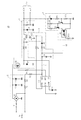
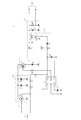
図1に、本発明の一実施形態に係る照明用電源装置10を示す。本実施形態に係る照明用電源装置10は、図5に示した従来の照明用電源装置11に放電回路1を追加したものである。なお、図1に示されている各構成要素のうち、図5と同一の符号を付した構成要素については従来技術で説明したものと同様なので、ここでは説明を一部省略する。
[Power supply for lighting]
FIG. 1 shows an illumination
放電回路1は、LED照明装置20に供給される直流出力電圧の低下を検出して検出信号を出力する出力電圧検出部と、上記検出信号が入力されているときにコンデンサC5の放電経路(第2放電経路X2)を形成する放電経路形成部とを含んでいる。
The
放電回路1の出力電圧検出部は、本発明の「第1スイッチ」に相当するツェナーダイオードZD1と、抵抗R9、R10、R11、R12と、本発明の「第2スイッチ」に相当するNPN型のトランジスタQ2と、本発明の「第3スイッチ」に相当するNPN型のトランジスタQ3と、フォトカプラPCの発光素子(本実施形態では、発光ダイオード)とを含んでいる。また、放電回路1の放電経路形成部は、フォトカプラPCの受光素子(本実施形態では、フォトトランジスタ)と、抵抗R13とを含んでいる。
The output voltage detection unit of the
ツェナーダイオードZD1は、カソードが照明用電源装置10のプラス側の出力端に接続され、アノードが抵抗R9および抵抗R10の直列回路を介してグラウンド接続されている。ツェナーダイオードZD1は、交流入力電圧が入力状態(ON)のときに導通状態(ON)になる一方、交流入力電圧が非入力状態(OFF)となりコンデンサC3の電圧が低下したとき(直流出力電圧が低下したとき)に非導通状態(OFF)となるように、ツェナー電圧(本発明の「閾値」に相当)が設定されている。
The Zener diode ZD1 has a cathode connected to the positive output terminal of the illumination
トランジスタQ2は、制御端子(ベース)が抵抗R9と抵抗R10の接続点に接続され、電流路の一端(コレクタ)が抵抗R11を介してツェナーダイオードZD1のカソードに接続され、電流路の他端(エミッタ)がグラウンド接続されている。 The transistor Q2 has a control terminal (base) connected to the connection point between the resistor R9 and the resistor R10, one end (collector) of the current path connected to the cathode of the Zener diode ZD1 via the resistor R11, and the other end ( Emitter) is grounded.
トランジスタQ3は、制御端子(ベース)がトランジスタQ2のコレクタに接続され、電流路の一端(コレクタ)が抵抗R12を介してツェナーダイオードZD1のカソードに接続され、電流路の他端(エミッタ)がフォトカプラPCの発光ダイオードを介してグラウンド接続されている。 The transistor Q3 has a control terminal (base) connected to the collector of the transistor Q2, one end (collector) of the current path connected to the cathode of the Zener diode ZD1 via the resistor R12, and the other end (emitter) of the current path It is grounded via the light emitting diode of the coupler PC.
フォトカプラPCの発光ダイオードは、アノードがトランジスタQ3のエミッタに接続されており、トランジスタQ3を経由した電流が流れると発光する。なお、発光ダイオードが発する光が、本発明の「検出信号」に相当する。 The light emitting diode of the photocoupler PC has an anode connected to the emitter of the transistor Q3, and emits light when a current flows through the transistor Q3. The light emitted from the light emitting diode corresponds to the “detection signal” of the present invention.
フォトカプラPCのフォトトランジスタは、電流路の一端(コレクタ)が電源電圧生成回路4のコンデンサC5と抵抗R8との接続点に接続され、電流路の他端(エミッタ)が抵抗R13を介してフレームグラウンドに接続されている。フォトカプラPCのフォトトランジスタは、発光ダイオードが発する光を受光しているときに導通する。言い換えれば、フォトトランジスタは、発光ダイオードからの検出信号が入力されているときにコンデンサC5の第2放電経路X2を形成する。 In the phototransistor of the photocoupler PC, one end (collector) of the current path is connected to a connection point between the capacitor C5 and the resistor R8 of the power supply voltage generation circuit 4, and the other end (emitter) of the current path is connected to the frame via the resistor R13. Connected to ground. The phototransistor of the photocoupler PC is turned on when receiving light emitted from the light emitting diode. In other words, the phototransistor forms the second discharge path X2 of the capacitor C5 when the detection signal from the light emitting diode is input.
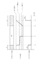
次に、図2を参照して、照明用電源装置10における調光制御と直流出力電流との関係について説明する。
Next, with reference to FIG. 2, the relationship between the dimming control in the illumination
制御回路U1では、動作電圧V1、スレッシュ電圧V2(例えば、約10.0V)、リセット電圧V3(例えば、約2.5V)が予め設定されており、スイッチ手段Q1のONデューティを切り替える順序(本実施形態では、100%→40%→2.5%)も予め設定されている。 In the control circuit U1, the operating voltage V1, the threshold voltage V2 (for example, about 10.0V), and the reset voltage V3 (for example, about 2.5V) are preset, and the order of switching the ON duty of the switch means Q1 (this In the embodiment, 100% → 40% → 2.5%) is also preset.
時刻t1の直前まで、制御回路U1は、ONデューティが40%になるようにスイッチ手段Q1のスイッチング動作を制御しており、LED照明装置20にはONデューティ40%に相当する直流出力電流が供給されている。このとき、放電回路1では、ツェナーダイオードZD1が導通状態、トランジスタQ2が導通状態、トランジスタQ3が非導通状態になるので、フォトカプラPCの発光ダイオードに電流が流れず、フォトカプラPCの発光ダイオードは光を発しない。このため、フォトカプラPCのフォトトランジスタは、非導通状態となり、コンデンサC5の第2放電経路X2を形成しない。
Immediately before the time t 1, the control circuit U1 is controlling the switching operation of the switching means Q1 to ON duty is 40%, the
交流入力電圧が入力状態(ON)から非入力状態(OFF)に切り替わると、電源電圧生成回路4のコンデンサC5は、当該コンデンサC5の一端と制御回路U1のVDD端子とを接続する経路(第1放電経路X1)で放電して制御回路U1にVDD電圧を供給する。これにより、VDD電圧は一気に低下する。時刻t1において、VDD電圧がスレッシュ電圧V2に達すると、制御回路U1がスイッチ手段Q1のスイッチング動作を停止させるので、LED照明装置20に供給される直流出力電流はゼロになる。
When the AC input voltage is switched from the input state (ON) to the non-input state (OFF), the capacitor C5 of the power supply voltage generation circuit 4 connects the one end of the capacitor C5 and the VDD terminal of the control circuit U1 (first It discharges in the discharge path X1) and supplies VDD voltage to the control circuit U1. As a result, the VDD voltage decreases at a stretch. At time t 1, when VDD voltage reaches the threshold voltage V2, the control circuit U1 is because to stop the switching operation of the switching means Q1, the DC output current supplied to the
また、制御回路U1がスイッチ手段Q1のスイッチング動作を停止させるとLED照明装置20に供給される直流出力電圧も低下する。直流出力電圧の低下によりツェナーダイオードZD1の両端に印加される電圧がツェナー電圧よりも小さくなると、放電回路1では、ツェナーダイオードZD1が非導通状態、トランジスタQ2が非導通状態、トランジスタQ3が導通状態に切り替わり、フォトカプラPCの発光ダイオードに電流が流れて、フォトカプラPCの発光ダイオードが光を発する。これにより、フォトカプラPCのフォトトランジスタは、導通状態となり、コンデンサC5の第2放電経路X2を形成する(時刻t2)。その結果、コンデンサC5が第2放電経路X2で放電するので、時刻t2において、VDD電圧は一気に低下してゼロになる。
Further, when the control circuit U1 stops the switching operation of the switch means Q1, the DC output voltage supplied to the
照明用電源装置10では、交流入力電圧が入力状態(ON)から非入力状態(OFF)に切り替わった後、第1放電経路X1での放電によりVDD電圧がリセット電圧V3以下になる前に、放電回路1が第2放電経路X2を形成するように、コンデンサC5の容量を
従来の照明用電源装置10におけるコンデンサC5の容量よりも大きくしている。例えば、従来の照明用電源装置11において、容量が2.2[μF]程度のコンデンサC5を使用する場合、本実施形態に係る照明用電源装置10では、容量が4.7[μF]程度のコンデンサC5を使用することが好ましい。
In the lighting
上述したように、放電回路1が第2放電経路X2を形成するとVDD電圧は一気に低下してゼロになるので、その後、時刻t3において交流入力電圧が非入力状態(OFF)から入力状態(ON)に切り替わり、時刻t4においてVDD電圧が動作電圧V1まで上昇すると、制御回路U1は、スイッチ手段Q1のONデューティが上記順序の最初の状態(100%の状態)に切り替わるように、スイッチ手段Q1のスイッチング動作を開始させる。これにより、LED照明装置20にはONデューティ100%に相当する直流出力電流が供給される(図2(C)参照)。
As described above, since the
結局、本実施形態に係る照明用電源装置10では、制御回路U1のVDD電圧がリセット電圧V3以下になる前にコンデンサC5を強制的に放電させる放電回路1を備えているので、リセット時間(交流入力電圧の非入力状態において、VDD電圧がスレッシュ電圧V2からリセット電圧V3に達するまでの時間)がリセット電圧V3に左右されることがなくなる。
After all, the illumination
[照明用電源システム]
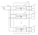
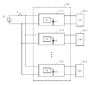
図3に、本発明の一実施形態に係る照明用電源システム100を示す。照明用電源システム100は、単一の交流電圧源30に対して複数(N個、Nは3以上の整数)の照明用電源装置10−1〜10−Nを並列に接続したものである。各照明用電源装置10−1〜10−Nの構成要素については、いずれも図1に示す照明用電源装置10と同様なので、ここでは説明を一部省略する。
[Power supply system for lighting]
FIG. 3 shows a lighting
照明用電源システム100では、交流電圧源30と照明用電源装置10−1〜10−Nの入力端との間に、スイッチSが設けられている。スイッチSが導通状態(ON)のときは、照明用電源装置10−1〜10−Nに対して交流入力電圧が入力状態(ON)になり、スイッチSが非導通状態(OFF)のときは、照明用電源装置10−1〜10−Nに対して交流入力電圧が非入力状態(OFF)になる。スイッチSは、例えば、照明用電源装置10−1〜10−Nが取り付けられた部屋の壁に設けることができる。
In the illumination
照明用電源装置10−1〜10−Nに備えられた制御回路U1〜UNは、いずれも動作電圧V1、スレッシュ電圧V2、リセット電圧V3が予め設定されており、スイッチ手段Q1のONデューティを切り替える順序(本実施形態では、100%→40%→2.5%)も予め設定されている。リセット電圧V3は、制御回路U1〜UNによってバラツキがある。 All of the control circuits U1 to UN provided in the illumination power supply devices 10-1 to 10-N are preset with the operating voltage V1, the threshold voltage V2, and the reset voltage V3, and switch the ON duty of the switch means Q1. The order (in this embodiment, 100% → 40% → 2.5%) is also preset. The reset voltage V3 varies depending on the control circuits U1 to UN.
照明用電源装置10−1〜10−Nに備えられた各放電回路1は、いずれも、VDD電圧が制御回路U1〜UNの各リセット電圧V3の最大値以下になる前に、第2放電経路X2を形成してコンデンサC5を強制的に放電させる。
Each of the
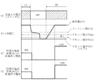
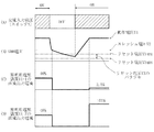
図4に、照明用電源システム100における調光制御と直流出力電流との関係を示す。照明用電源システム100では、照明用電源装置10−1に備えられた制御回路U1のリセット電圧V3が最も小さく、照明用電源装置10−2に備えられた制御回路U2のリセット電圧V3が最も大きいものとする。そして、制御回路U1のリセット電圧V3をV3MINとし、制御回路U2のリセット電圧V3をV3MAXとする。
FIG. 4 shows the relationship between the dimming control and the DC output current in the illumination
照明用電源システム100では、図4(A)および(B)に示すように、交流入力電圧が入力状態(ON)から非入力状態(OFF)に切り替わると、照明用電源装置10−1〜10−Nに備えられた各放電回路1は、各制御回路U1〜UNのVDD電圧がリセット電圧V3MAX以下になる前に、第2放電経路X2を形成してコンデンサC5を強制的に放電させる。これにより、各制御回路U1〜UNのVDD電圧は、いずれもゼロになる。
In the illumination
その後、交流入力電圧が非入力状態(OFF)から入力状態(ON)に切り替わると、各制御回路U1〜UNは、各スイッチ手段Q1のONデューティが上記順序の最初の状態(100%の状態)に切り替わるように、各スイッチ手段Q1のスイッチング動作を開始させる。これにより、LED照明装置20−1および20−2には、ONデューティ100%に相当する直流出力電流が供給される(図4(C)および(D)参照)。当然ながら、残りのLED照明装置20−3〜20−Nにも、ONデューティ100%に相当する直流出力電流が供給される。 Thereafter, when the AC input voltage is switched from the non-input state (OFF) to the input state (ON), each of the control circuits U1 to UN has an ON duty of each switch means Q1 in an initial state (100% state) in the above order. The switching operation of each switch means Q1 is started so as to switch to As a result, a DC output current corresponding to an ON duty of 100% is supplied to the LED lighting devices 20-1 and 20-2 (see FIGS. 4C and 4D). Of course, the remaining LED lighting devices 20-3 to 20-N are also supplied with a DC output current corresponding to an ON duty of 100%.
結局、照明用電源システム100では、各照明用電源装置10−1〜10−Nは、VDD電圧がリセット電圧V3の最大値(リセット電圧V3MAX)以下になる前にコンデンサC5を強制的に放電させる放電回路1を備えているので、リセット時間がリセット電圧V3のバラツキに左右されることがなくなる。その結果、照明用電源システム100によれば、図7に示す従来の照明用電源システム101のようにLED照明装置20−1とLED照明装置20−2との明るさが異なってしまうということはなく、LED照明装置20−1〜20−Nの明るさを揃えて切り替えることができる安定した調光制御が可能になる。
Eventually, in the illumination
以上、本発明に係る照明用電源装置および照明用電源システムの実施形態について説明したが、本発明は上記実施形態に限定されるものではない。 As mentioned above, although embodiment of the power supply device for illumination and the power supply system for illumination which concern on this invention was described, this invention is not limited to the said embodiment.
例えば、放電回路1は、入力電圧が入力状態(ON)から非入力状態(OFF)に切り替わった後、電源電圧(VDD電圧)がリセット電圧V3以下になる前に新たな放電経路を形成し、電源電圧を供給するコンデンサC5を強制的に放電させることができるのであれば、その構成を適宜変更することができる。
For example, the
整流平滑回路2の構成も適宜変更することができ、入力電圧が直流の場合は、整流平滑回路2自体を省略することができる。また、出力電流生成回路3は、スイッチング動作により出力電流を生成するスイッチ手段Q1を含むのであれば、その構成を適宜変更することができる。
The configuration of the rectifying /
制御回路U1は、入力電圧に応じた電源電圧が供給され、入力電圧が非入力状態(OFF)から入力状態(ON)に切り替わった際、電源電圧の電圧値が予め設定されたリセット電圧V3よりも大きい場合は、出力電流の電流量が予め設定された順序に従って切り替わる一方、電源電圧の電圧値がリセット電圧V3よりも小さい場合は出力電流の電流量が上記順序の最初の状態に切り替わるように、スイッチ手段Q1を制御する回路であれば、適宜用いることができる。また、制御回路U1は、スイッチ手段Q1のONデューティを2段階で切り替えてもよいし、4段階以上で切り替えてもよい。 The control circuit U1 is supplied with a power supply voltage corresponding to the input voltage, and when the input voltage is switched from the non-input state (OFF) to the input state (ON), the voltage value of the power supply voltage is set from a preset reset voltage V3. Is larger than the reset voltage V3, the current amount of the output current is switched to the first state in the above order. Any circuit that controls the switch means Q1 can be used as appropriate. Further, the control circuit U1 may switch the ON duty of the switch means Q1 in two stages or in four or more stages.
電源電圧生成回路4は、入力電圧が入力状態(ON)のときに充電され、かつ入力電圧が非入力状態(OFF)のときに放電して制御回路U1に電源電圧を供給するコンデンサC5を含むのであれば、その構成を適宜変更することができる。 The power supply voltage generation circuit 4 includes a capacitor C5 that is charged when the input voltage is in the input state (ON) and is discharged when the input voltage is in the non-input state (OFF) to supply the power supply voltage to the control circuit U1. If it is, the structure can be changed suitably.
上記実施形態における照明用電源システム100は、N台の照明用電源装置10を備えているが、本発明に係る照明用電源システムは、少なくとも2台の照明用電源装置10を備えていればよい。
The illumination
上記実施形態では、照明装置としてLED照明装置20を例に挙げて説明しているが、供給される出力電流の電流量に応じて明るさが変わるものであれば、LED照明装置20以外の照明装置を使用することができる。
In the above embodiment, the
1 放電回路
2 整流平滑回路
3 出力電流生成回路
4 電源電圧生成回路
10 照明用電源装置
20 LED照明装置
30 交流電圧源
100 照明用電源システム
DESCRIPTION OF
Claims (6)
スイッチング動作により前記出力電流を生成するスイッチ手段と、
前記入力電圧に応じた電源電圧が供給され、前記非入力状態から前記入力状態に切り替わった際、前記電源電圧の電圧値が予め設定されたリセット電圧よりも大きい場合は前記出力電流の電流量が前記順序に従って切り替わる一方、前記電源電圧の電圧値が前記リセット電圧よりも小さい場合は前記出力電流の電流量が前記順序の最初の状態に切り替わるように、前記スイッチ手段を制御する制御回路と、
前記入力状態のときに充電され、かつ前記非入力状態のときに第1放電経路で放電して前記制御回路に前記電源電圧を供給するコンデンサと、
前記入力状態から前記非入力状態に切り替わった後、前記第1放電経路での放電により前記電源電圧が前記リセット電圧以下になる前に、前記第1放電経路とは異なる第2放電経路を形成して前記コンデンサを放電させる放電回路と、
を備えたことを特徴とする照明用電源装置。 In accordance with repetition of the input state of the input voltage and the non-input state of the input voltage, a lighting power supply device that switches the amount of output current to be supplied to the lighting device step by step in a preset order,
Switch means for generating the output current by a switching operation;
When a power supply voltage corresponding to the input voltage is supplied and the voltage value of the power supply voltage is larger than a preset reset voltage when the non-input state is switched to the input state, the current amount of the output current is A control circuit for controlling the switch means so that the amount of the output current is switched to the first state of the sequence when the voltage value of the power supply voltage is smaller than the reset voltage, while switching according to the sequence;
A capacitor that is charged in the input state and discharges in a first discharge path in the non-input state to supply the power supply voltage to the control circuit;
After switching from the input state to the non-input state, a second discharge path different from the first discharge path is formed before the power supply voltage becomes equal to or lower than the reset voltage due to discharge in the first discharge path. A discharge circuit for discharging the capacitor;
An illumination power supply device comprising:
前記照明装置に供給される出力電圧の低下を検出し、前記出力電圧が所定の閾値よりも小さくなると検出信号を出力する出力電圧検出部と、
前記検出信号が入力されているときに前記第2放電経路を形成する放電経路形成部と、
を含むことを特徴とする請求項1に記載の照明用電源装置。 The discharge circuit is:
An output voltage detector that detects a decrease in the output voltage supplied to the lighting device and outputs a detection signal when the output voltage is smaller than a predetermined threshold;
A discharge path forming unit that forms the second discharge path when the detection signal is input;
The illumination power supply device according to claim 1, comprising:
前記出力電圧が前記閾値よりも小さくなると非導通状態になる第1スイッチと、
前記第1スイッチが非導通状態になると非導通状態になる第2スイッチと、
前記第2スイッチが非導通状態になると導通状態になる第3スイッチと、
前記第3スイッチが導通状態になると前記検出信号として光を発する発光素子と、
を含み、
前記放電経路形成部は、
前記発光素子の光を受光しているときに前記第2放電経路を形成する受光素子を含む
ことを特徴とする請求項2に記載の照明用電源装置。 The output voltage detector is
A first switch that becomes non-conductive when the output voltage is less than the threshold;
A second switch that is non-conductive when the first switch is non-conductive;
A third switch that is conductive when the second switch is non-conductive;
A light emitting element that emits light as the detection signal when the third switch is turned on;
Including
The discharge path forming part is
The illumination power supply apparatus according to claim 2, further comprising a light receiving element that forms the second discharge path when receiving light from the light emitting element.
前記照明用電源装置は、
スイッチング動作により前記出力電流を生成するスイッチ手段と、
前記入力電圧に応じた電源電圧が供給され、前記非入力状態から前記入力状態に切り替わった際、前記電源電圧の電圧値がリセット電圧よりも大きい場合は前記出力電流の電流量が前記順序に従って切り替わる一方、前記電源電圧の電圧値が前記リセット電圧よりも小さい場合は前記出力電流の電流量が前記順序の最初の状態に切り替わるように、前記スイッチ手段を制御する制御回路と、
前記入力状態のときに充電され、かつ前記非入力状態のときに第1放電経路で放電して前記制御回路に前記電源電圧を供給するコンデンサと、
前記第1放電経路とは異なる第2放電経路を形成して前記コンデンサを放電させる放電回路と、
を備え、
前記リセット電圧は、前記制御回路ごとに予め設定されており、
前記放電回路は、前記入力状態から前記非入力状態に切り替わった後、前記第1放電経路での放電により前記電源電圧が、前記制御回路ごとに予め設定されたリセット電圧の最大値以下になる前に、前記第2放電経路を形成して前記コンデンサを放電させる
ことを特徴とする照明用電源システム。 A plurality of lighting power supplies each having an input connected to a single voltage source and an output connected to a separate lighting device, each of the plurality of lighting power supplies from the voltage source For lighting that switches the current amount of the output current supplied to the lighting device connected to the output terminal stepwise in a preset order according to the repetition of the input state of the input voltage and the non-input state of the input voltage A power system,
The lighting power supply device comprises:
Switch means for generating the output current by a switching operation;
When the power supply voltage corresponding to the input voltage is supplied and the voltage value of the power supply voltage is larger than the reset voltage when the non-input state is switched to the input state, the current amount of the output current is switched according to the order. On the other hand, when the voltage value of the power supply voltage is smaller than the reset voltage, a control circuit that controls the switch means so that the amount of the output current is switched to the first state of the sequence;
A capacitor that is charged in the input state and discharges in a first discharge path in the non-input state to supply the power supply voltage to the control circuit;
A discharge circuit for discharging the capacitor by forming a second discharge path different from the first discharge path;
With
The reset voltage is preset for each control circuit,
After the discharge circuit is switched from the input state to the non-input state, before the power supply voltage becomes equal to or less than a maximum value of a reset voltage preset for each control circuit due to discharge in the first discharge path. In addition, the illumination power supply system is characterized in that the capacitor is discharged by forming the second discharge path.
前記照明装置に供給される出力電圧の低下を検出し、前記出力電圧が所定の閾値よりも小さくなると検出信号を出力する出力電圧検出部と、
前記検出信号が入力されているときに前記第2放電経路を形成する放電経路形成部と、
を含むことを特徴とする請求項4に記載の照明用電源システム。 The discharge circuit is:
An output voltage detector that detects a decrease in the output voltage supplied to the lighting device and outputs a detection signal when the output voltage is smaller than a predetermined threshold;
A discharge path forming unit that forms the second discharge path when the detection signal is input;
The illumination power supply system according to claim 4, comprising:
前記出力電圧が前記閾値よりも小さくなると非導通状態になる第1スイッチと、
前記第1スイッチが非導通状態になると非導通状態になる第2スイッチと、
前記第2スイッチが非導通状態になると導通状態になる第3スイッチと、
前記第3スイッチが導通状態になると前記検出信号として光を発する発光素子と、
を含み、
前記放電経路形成部は、
前記発光素子の光を受光しているときに前記第2放電経路を形成する受光素子を含む
ことを特徴とする請求項5に記載の照明用電源システム。 The output voltage detector is
A first switch that becomes non-conductive when the output voltage is less than the threshold;
A second switch that is non-conductive when the first switch is non-conductive;
A third switch that is conductive when the second switch is non-conductive;
A light emitting element that emits light as the detection signal when the third switch is turned on;
Including
The discharge path forming part is
The illumination power supply system according to claim 5, further comprising a light receiving element that forms the second discharge path when receiving light from the light emitting element.
Priority Applications (1)
| Application Number | Priority Date | Filing Date | Title |
|---|---|---|---|
| JP2014210051A JP6282012B2 (en) | 2014-10-14 | 2014-10-14 | LIGHTING POWER DEVICE AND LIGHTING POWER SYSTEM |
Applications Claiming Priority (1)
| Application Number | Priority Date | Filing Date | Title |
|---|---|---|---|
| JP2014210051A JP6282012B2 (en) | 2014-10-14 | 2014-10-14 | LIGHTING POWER DEVICE AND LIGHTING POWER SYSTEM |
Publications (2)
| Publication Number | Publication Date |
|---|---|
| JP2016081644A JP2016081644A (en) | 2016-05-16 |
| JP6282012B2 true JP6282012B2 (en) | 2018-02-21 |
Family
ID=55958901
Family Applications (1)
| Application Number | Title | Priority Date | Filing Date |
|---|---|---|---|
| JP2014210051A Active JP6282012B2 (en) | 2014-10-14 | 2014-10-14 | LIGHTING POWER DEVICE AND LIGHTING POWER SYSTEM |
Country Status (1)
| Country | Link |
|---|---|
| JP (1) | JP6282012B2 (en) |
Families Citing this family (1)
| Publication number | Priority date | Publication date | Assignee | Title |
|---|---|---|---|---|
| CN108882429B (en) * | 2017-05-15 | 2022-03-15 | 松下知识产权经营株式会社 | Lighting device and illumination system |
Family Cites Families (3)
| Publication number | Priority date | Publication date | Assignee | Title |
|---|---|---|---|---|
| JP4785804B2 (en) * | 2006-08-04 | 2011-10-05 | 三菱電機株式会社 | Discharge lamp lighting device, lighting fixture, lighting system, and output indicator |
| JP2010073575A (en) * | 2008-09-19 | 2010-04-02 | Panasonic Electric Works Co Ltd | Lighting device, illuminating equipment using the same, and illuminating system |
| TWI478627B (en) * | 2012-04-20 | 2015-03-21 | Lextar Electronics Corp | Illuminating device capable of adjusting brightness and brightness adjusting method thereof |
-
2014
- 2014-10-14 JP JP2014210051A patent/JP6282012B2/en active Active
Also Published As
| Publication number | Publication date |
|---|---|
| JP2016081644A (en) | 2016-05-16 |
Similar Documents
| Publication | Publication Date | Title |
|---|---|---|
| TWI489911B (en) | Active bleeder circuit triggering triac in all phase and light emitting device power supply circuit and triac control method using the active bleeder circuit | |
| US8183795B2 (en) | LED current-supplying circuit and LED current-controlling circuit | |
| KR102257718B1 (en) | Circuit driving light emitting diode and light apparatus comprising the same | |
| US9655176B2 (en) | LED light source | |
| CN103428959A (en) | Components and methods for driving LED lamps | |
| JP5822670B2 (en) | LED lighting device | |
| US10356867B2 (en) | Light-dimming device | |
| US10070492B2 (en) | Dimming device | |
| KR101536108B1 (en) | Control circuit and voltage generating method for led lighting apparatus | |
| RU2017146373A (en) | LED LIGHT SOURCE WITH IMPROVED REDUCTION REDUCTION | |
| TW201507542A (en) | Light-emitting diode system and voltage conversion device | |
| JP6282012B2 (en) | LIGHTING POWER DEVICE AND LIGHTING POWER SYSTEM | |
| US10736188B2 (en) | Lighting control device | |
| JP7012267B2 (en) | Lighting device and lighting system | |
| KR20180071293A (en) | Light Emitting Diode Lighting Device | |
| JP6396793B2 (en) | Switching power supply circuit | |
| EP3349545A1 (en) | Lighting control device | |
| JP6777449B2 (en) | Power supply for LED strobe light emission | |
| JP6101744B2 (en) | Switching power supply | |
| JP5954653B2 (en) | Dimming signal converter and lighting system using the same | |
| KR20130034377A (en) | A lighting control circuit for led lighting | |
| JP2019207833A (en) | Power supply device for illumination | |
| JP2018201298A (en) | Light source lighting device and lighting apparatus | |
| JP5009357B2 (en) | Power supply device and lighting device | |
| JP2018063878A (en) | LED lighting power supply device and LED lighting device |
Legal Events
| Date | Code | Title | Description |
|---|---|---|---|
| A621 | Written request for application examination |
Free format text: JAPANESE INTERMEDIATE CODE: A621 Effective date: 20170410 |
|
| A977 | Report on retrieval |
Free format text: JAPANESE INTERMEDIATE CODE: A971007 Effective date: 20180111 |
|
| TRDD | Decision of grant or rejection written | ||
| A01 | Written decision to grant a patent or to grant a registration (utility model) |
Free format text: JAPANESE INTERMEDIATE CODE: A01 Effective date: 20180117 |
|
| A61 | First payment of annual fees (during grant procedure) |
Free format text: JAPANESE INTERMEDIATE CODE: A61 Effective date: 20180122 |
|
| R150 | Certificate of patent or registration of utility model |
Ref document number: 6282012 Country of ref document: JP Free format text: JAPANESE INTERMEDIATE CODE: R150 |
|
| R250 | Receipt of annual fees |
Free format text: JAPANESE INTERMEDIATE CODE: R250 |
|
| R250 | Receipt of annual fees |
Free format text: JAPANESE INTERMEDIATE CODE: R250 |
|
| R250 | Receipt of annual fees |
Free format text: JAPANESE INTERMEDIATE CODE: R250 |
|
| R250 | Receipt of annual fees |
Free format text: JAPANESE INTERMEDIATE CODE: R250 |
|
| R250 | Receipt of annual fees |
Free format text: JAPANESE INTERMEDIATE CODE: R250 |
|
| R250 | Receipt of annual fees |
Free format text: JAPANESE INTERMEDIATE CODE: R250 |