JP6282000B6 - Power amplifier - Google Patents
Power amplifier Download PDFInfo
- Publication number
- JP6282000B6 JP6282000B6 JP2017525188A JP2017525188A JP6282000B6 JP 6282000 B6 JP6282000 B6 JP 6282000B6 JP 2017525188 A JP2017525188 A JP 2017525188A JP 2017525188 A JP2017525188 A JP 2017525188A JP 6282000 B6 JP6282000 B6 JP 6282000B6
- Authority
- JP
- Japan
- Prior art keywords
- processing unit
- phase
- switching
- sine wave
- filter
- Prior art date
- Legal status (The legal status is an assumption and is not a legal conclusion. Google has not performed a legal analysis and makes no representation as to the accuracy of the status listed.)
- Active
Links
- 238000004364 calculation method Methods 0.000 claims description 37
- 230000007274 generation of a signal involved in cell-cell signaling Effects 0.000 claims description 25
- 238000005562 fading Methods 0.000 claims description 11
- 230000010363 phase shift Effects 0.000 claims description 2
- 230000003321 amplification Effects 0.000 description 16
- 238000003199 nucleic acid amplification method Methods 0.000 description 16
- 238000006243 chemical reaction Methods 0.000 description 10
- 238000010586 diagram Methods 0.000 description 9
- 238000000034 method Methods 0.000 description 8
- 238000013139 quantization Methods 0.000 description 7
- 238000010606 normalization Methods 0.000 description 5
- 238000001914 filtration Methods 0.000 description 3
- 238000009825 accumulation Methods 0.000 description 2
- 239000000470 constituent Substances 0.000 description 2
- 238000004891 communication Methods 0.000 description 1
- 238000007796 conventional method Methods 0.000 description 1
- 238000004519 manufacturing process Methods 0.000 description 1
- 238000003672 processing method Methods 0.000 description 1
Images


Classifications
-
- H—ELECTRICITY
- H03—ELECTRONIC CIRCUITRY
- H03F—AMPLIFIERS
- H03F3/00—Amplifiers with only discharge tubes or only semiconductor devices as amplifying elements
- H03F3/20—Power amplifiers, e.g. Class B amplifiers, Class C amplifiers
- H03F3/21—Power amplifiers, e.g. Class B amplifiers, Class C amplifiers with semiconductor devices only
- H03F3/217—Class D power amplifiers; Switching amplifiers
- H03F3/2173—Class D power amplifiers; Switching amplifiers of the bridge type
-
- H—ELECTRICITY
- H03—ELECTRONIC CIRCUITRY
- H03F—AMPLIFIERS
- H03F3/00—Amplifiers with only discharge tubes or only semiconductor devices as amplifying elements
- H03F3/20—Power amplifiers, e.g. Class B amplifiers, Class C amplifiers
- H03F3/21—Power amplifiers, e.g. Class B amplifiers, Class C amplifiers with semiconductor devices only
- H03F3/217—Class D power amplifiers; Switching amplifiers
- H03F3/2171—Class D power amplifiers; Switching amplifiers with field-effect devices
-
- H—ELECTRICITY
- H03—ELECTRONIC CIRCUITRY
- H03F—AMPLIFIERS
- H03F3/00—Amplifiers with only discharge tubes or only semiconductor devices as amplifying elements
- H03F3/20—Power amplifiers, e.g. Class B amplifiers, Class C amplifiers
- H03F3/21—Power amplifiers, e.g. Class B amplifiers, Class C amplifiers with semiconductor devices only
- H03F3/217—Class D power amplifiers; Switching amplifiers
- H03F3/2175—Class D power amplifiers; Switching amplifiers using analogue-digital or digital-analogue conversion
-
- H—ELECTRICITY
- H03—ELECTRONIC CIRCUITRY
- H03F—AMPLIFIERS
- H03F3/00—Amplifiers with only discharge tubes or only semiconductor devices as amplifying elements
- H03F3/20—Power amplifiers, e.g. Class B amplifiers, Class C amplifiers
- H03F3/24—Power amplifiers, e.g. Class B amplifiers, Class C amplifiers of transmitter output stages
-
- H—ELECTRICITY
- H03—ELECTRONIC CIRCUITRY
- H03K—PULSE TECHNIQUE
- H03K5/00—Manipulating of pulses not covered by one of the other main groups of this subclass
- H03K5/01—Shaping pulses
- H03K5/02—Shaping pulses by amplifying
-
- H—ELECTRICITY
- H03—ELECTRONIC CIRCUITRY
- H03M—CODING; DECODING; CODE CONVERSION IN GENERAL
- H03M1/00—Analogue/digital conversion; Digital/analogue conversion
- H03M1/06—Continuously compensating for, or preventing, undesired influence of physical parameters
- H03M1/0617—Continuously compensating for, or preventing, undesired influence of physical parameters characterised by the use of methods or means not specific to a particular type of detrimental influence
- H03M1/0626—Continuously compensating for, or preventing, undesired influence of physical parameters characterised by the use of methods or means not specific to a particular type of detrimental influence by filtering
- H03M1/0629—Anti-aliasing
-
- H—ELECTRICITY
- H04—ELECTRIC COMMUNICATION TECHNIQUE
- H04L—TRANSMISSION OF DIGITAL INFORMATION, e.g. TELEGRAPHIC COMMUNICATION
- H04L27/00—Modulated-carrier systems
- H04L27/32—Carrier systems characterised by combinations of two or more of the types covered by groups H04L27/02, H04L27/10, H04L27/18 or H04L27/26
- H04L27/34—Amplitude- and phase-modulated carrier systems, e.g. quadrature-amplitude modulated carrier systems
- H04L27/36—Modulator circuits; Transmitter circuits
- H04L27/362—Modulation using more than one carrier, e.g. with quadrature carriers, separately amplitude modulated
Landscapes
- Engineering & Computer Science (AREA)
- Power Engineering (AREA)
- Theoretical Computer Science (AREA)
- Computer Networks & Wireless Communication (AREA)
- Signal Processing (AREA)
- Physics & Mathematics (AREA)
- Nonlinear Science (AREA)
- Amplifiers (AREA)
Description
本発明は、無線通信における電力増幅の方法、特に、D級電力増幅器を用いた電力増幅装置に関する。 The present invention relates to a power amplification method in wireless communication, and more particularly to a power amplification device using a class D power amplifier.
アウトフェージング方式の電力増幅は、D級電力増幅器の使用により、高効率な電力増幅が可能な方式である(例えば、特許文献1参照)。
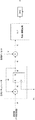
そこで、アウトフェージング方式の電力増幅の概要について、図4を用いて説明する。図4は、フルブリッジ型のD級電力増幅器を使用したアウトフェージング方式の電力増幅装置を示す図である。Out-fading power amplification is a method that enables high-efficiency power amplification by using a class D power amplifier (see, for example, Patent Document 1).
Therefore, an outline of out-fading power amplification will be described with reference to FIG. FIG. 4 is a diagram illustrating an out-fading power amplifier using a full-bridge class D power amplifier.
図4においては、4つのゲート端子(G1〜G4)に対して、送信する変調波信号に基づいて生成したスイッチング用信号を入力する。この結果、D級電力増幅器101の出力として、矩形波状の信号が出力される。この出力信号には、所望の変調波信号と高調波成分とが含まれている。そこで、D級電力増幅器101の後段で、フィルタ102を用いてフィルタリングを実施し、所望の変調波信号を取り出している。 In FIG. 4, a switching signal generated based on a modulated wave signal to be transmitted is input to four gate terminals (G1 to G4). As a result, a rectangular wave signal is output as the output of the class
ここで、図4の4つのゲート端子(G1〜G4)に入力するスイッチング用信号について、図5を用いて説明する。図5は、各ゲート端子(G1〜G4)に対するスイッチング用信号の与え方の例を示す図である。図5(a)はゲート端子G1に入力するスイッチング用信号を示し、図5(b)はゲート端子G3に入力するスイッチング用信号を示し、図5(c)は図4のA点における増幅器出力信号を示し、また、図5(d)は図4のB点におけるフィルタ出力信号を示している。
なお、ここでは、説明を簡略化するため、AM変調の場合を示しており、図中のTは搬送波の周期である。Here, switching signals input to the four gate terminals (G1 to G4) in FIG. 4 will be described with reference to FIG. FIG. 5 is a diagram illustrating an example of how to provide a switching signal to each gate terminal (G1 to G4). 5A shows the switching signal input to the gate terminal G1, FIG. 5B shows the switching signal input to the gate terminal G3, and FIG. 5C shows the amplifier output at point A in FIG. FIG. 5D shows the filter output signal at point B in FIG.
Here, in order to simplify the explanation, the case of AM modulation is shown, and T in the figure is the period of the carrier wave.
図5に示すように、図4のA点では、「G1、G4がオン」、かつ、「G3、G2がオフ」で、正となり、逆に、「G1、G4がオフ」、かつ、「G3、G2がオン」で、負となる。これを利用し、G1およびG2(=−G1)の変化タイミング、G3およびG4(=−G3)の変化タイミングを制御することで、A点での矩形波状の信号の波形を変化させている。 As shown in FIG. 5, at point A in FIG. 4, “G1 and G4 are on” and “G3 and G2 are off” become positive, and conversely, “G1 and G4 are off” and “ When “G3 and G2 are ON”, it becomes negative. By utilizing this, the change timing of G1 and G2 (= −G1) and the change timing of G3 and G4 (= −G3) are controlled to change the waveform of the rectangular wave signal at point A.
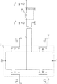
次に、図4の4つのゲート端子(G1〜G4)に入力するスイッチング用信号の生成方法について、図6を用いて説明する。図6は、図4の4つのゲート端子(G1〜G4)に与えるスイッチング用信号生成回路の構成を示すブロック図である。 Next, a method for generating switching signals input to the four gate terminals (G1 to G4) in FIG. 4 will be described with reference to FIG. FIG. 6 is a block diagram showing a configuration of a switching signal generation circuit applied to the four gate terminals (G1 to G4) of FIG.
従来のスイッチング用信号生成回路は、図6に示すように、変調処理部1と、補間処理部2と、振幅算出処理部3と、振幅−位相変換処理部4と、乗算処理部5と、位相算出処理部6と、加算処理部7と、正規化処理部18と、ON区間算出処理部19と、量子化処理部20と、カウンタ21と、比較処理部22と、反転処理部23とから構成されている。 As shown in FIG. 6, the conventional switching signal generation circuit includes a
従来のスイッチング用信号生成回路では、まず、変調処理部1で送信する変調信号を生成し、補間処理部2により、搬送波周波数(または、それに準ずる周波数)のレートにアップサンプリングする。
補間処理部2でのアップサンプリングの後、サンプルごとに、振幅算出処理部3および位相算出処理部6で、極形式表現(振幅値、位相値)に変換する。In a conventional switching signal generation circuit, first, a modulation signal to be transmitted is generated by the
After the upsampling in the
極形式表現に変換した後、振幅−位相変換処理部4で、振幅値を角度値φに変換する。この角度値φで、G1、G3への制御パルスの相対関係を調整する。なお、G1側をφ/2進め、G3側をφ/2遅らせることで、相対関係を調整している。このため、乗算処理部5で角度値φを半分にしている。
この後、加算処理部7では、乗算処理部5からの角度値φ/2と、位相算出処理部6からの位相値θとにより、G1用制御パルスの位相(θ+φ/2)、G3用制御パルスの位相(θ−φ/2+π)を生成する。After conversion to polar format representation, the amplitude-phase
Thereafter, the addition processing unit 7 uses the angle value φ / 2 from the
さらに、正規化処理部18、ON区間算出処理部19、量子化処理部20、カウンタ21、比較処理部22、反転処理部23により、G1用、G3用に生成した位相を、スイッチングのためのパルス信号に変換している。
カウンタ21は、搬送波周期より十分短い周期で値を更新し、搬送波周期で元の値に戻るように動作させている。(例えば、搬送波周期の1/64の周期で、0から63まで、1ずつカウントアップした後、0に戻る動作を繰り返す。)Further, the phases generated for G1 and G3 by the
The
一方、カウント値の判定基準となる値は、正規化処理部18、ON区間算出処理部19、量子化処理部20で算出する。まず、正規化処理部18で、0〜2πの位相を、0〜1の範囲に正規化する。その後、ON区間算出処理部19で、ONの範囲を、0〜1の範囲のどの範囲にするか、定める。(例えば、θ=0、φ/2=0であれば、
G1、G2(=−G1)用ON区間は、0〜0.5 G3、G4(=−G3)用ON区間は、0.5〜1 θ=0、φ/2=π/4であれば、
G1、G2(=−G1)用ON区間は、0〜0.375および0.875〜1 G3、G4(=−G3)用ON区間は、0〜0.125および0.625〜1など。)
さらに、カウンタ値の語長に基づき、量子化処理部20で判定基準値を量子化する。(例えば、前述の6ビットカウンタ(0〜63)との比較であれば、ON区間算出処理部19の出力に64を乗じて、小数点第1位で四捨五入する。) 以上により、カウンタ21の値に応じて、各スイッチング用信号のオン/オフが切り替わる。On the other hand, a value serving as a determination criterion for the count value is calculated by the
The ON section for G1, G2 (= −G1) is 0 to 0.5. The ON section for G3, G4 (= −G3) is 0.5 to 1 θ = 0, φ / 2 = π / 4. ,
G1, G2 (= -G1) ON sections are 0-0.375 and 0.875-1 G3, G4 (= -G3) ON sections are 0-0.125, 0.625-1, etc. )
Further, based on the word length of the counter value, the
従来方式の場合、スイッチング用信号のオン/オフのタイミングの精度が、搬送波周期Tの中をどこまでの分解能で処理するかに影響される。具体的には、実現できるタイミングの数が、図6のカウンタ21で表せる状態数に制限されるということであり、制限する際に、時間軸方向の量子化が、別途、必要になっているということである。この量子化が、D級電力増幅器の出力波形と理想スイッチング時の出力波形との差異を生じさせる。この差異の影響は、最終的なフィルタリング後にも、変調波の帯域内/帯域外の雑音として観測され、帯域外領域のスプリアス特性やEVM(Error Vector Magnitude)等、各種特性が劣化する。
従って、図6のカウンタ21の更新と、比較処理部22における比較処理は、雑音の発生レベルが許容できる程度になる、十分に高い動作クロックで実施する必要があることになる。In the case of the conventional method, the accuracy of the on / off timing of the switching signal is affected by how much resolution is processed in the carrier wave period T. Specifically, the number of timings that can be realized is limited to the number of states that can be represented by the
Therefore, the updating of the
しかし、同時に、無線周波数の制約で、ディジタル回路の動作クロックを無条件に高くできないことも考慮しなければならない。例えば、無線周波数(搬送波周波数)が100MHzであるとし、スイッチング信号を100MHzの周期の1/64の分解能で制御しようとしただけでも、ロジックの動作クロックは、6.4GHzとなる。このような高い動作クロックが必須になってしまうことは、ハードウェア実現を困難にする要因になる。 However, at the same time, it must be considered that the operating clock of the digital circuit cannot be unconditionally increased due to radio frequency constraints. For example, assuming that the radio frequency (carrier frequency) is 100 MHz and the switching signal is only controlled with a resolution of 1/64 of the cycle of 100 MHz, the logic operation clock is 6.4 GHz. The necessity of such a high operating clock is a factor that makes it difficult to implement hardware.
本発明は、この様な状況に鑑みて為されたものであり、スイッチング用信号生成処理において、パルス生成時のディジタル回路の動作クロックの制約を解決し、アウトフェージング方式電力増幅を適用可能な無線周波数範囲を拡大することが可能な電力増幅装置を提供することを目的とする。 The present invention has been made in view of such a situation. In switching signal generation processing, the present invention solves the limitation of the operation clock of the digital circuit at the time of pulse generation and can apply outphasing power amplification. An object of the present invention is to provide a power amplifying device capable of expanding the frequency range.
上記目的を達成するために、本発明に係る電力増幅装置は、フルブリッジ型のD級電力増幅器を有するアウトフェージング方式の電力増幅装置において、送信する変調波の振幅、位相に基づき、2種類の搬送波周波数の正弦波を生成し、生成した正弦波から、前記D級電力増幅器をスイッチングするためのスイッチング用パルス信号を生成するスイッチング用信号生成回路を備え、前記スイッチング用信号生成回路は、生成された2種類の正弦波の位相情報を直交形式に変換するsin算出処理部およびcos算出処理部と、前記sin算出処理部および前記cos算出処理部から入力された各々の直交形式の位相情報をアナログ信号に変換するDA変換器と、前記DA変換器から入力されたアナログ信号から折り返し成分を除去する第1のフィルタと、前記第1のフィルタから入力されたアナログ信号から、ローカル信号を用いて正弦波を生成するアナログ直交変調器と、前記アナログ直交変調器から入力された正弦波から所定の無線周波数およびその近傍の成分を通過させる第2のフィルタと、基準電圧との比較により、前記第2のフィルタから入力された正弦波からスイッチング用パルス信号への変換を行うコンパレータと、を有することを特徴とする。 To achieve the above object, the power amplifying device according to the present invention is an out-fading power amplifying device having a full-bridge type D power amplifier, and is based on the amplitude and phase of a modulated wave to be transmitted. A switching signal generating circuit for generating a switching pulse signal for generating a switching pulse signal for switching the class D power amplifier from the generated sine wave, and generating the switching signal generating circuit; The sin calculation processing unit and the cos calculation processing unit that convert the phase information of the two types of sine waves into the orthogonal format, and the phase information in the orthogonal format input from the sin calculation processing unit and the cos calculation processing unit are analogized. A DA converter that converts the signal into a signal, and a first component that removes the aliasing component from the analog signal input from the DA converter. Filter, an analog quadrature modulator that generates a sine wave using a local signal from the analog signal input from the first filter, a predetermined radio frequency from the sine wave input from the analog quadrature modulator, and its A second filter that passes nearby components; and a comparator that converts a sine wave input from the second filter into a switching pulse signal by comparison with a reference voltage. .
また、上記目的を達成するために、本発明に係る電力増幅装置は、上記した電力増幅装置において、前記直交形式の位相情報は、所定の間隔で、送信する前記変調波に基づいて更新することを特徴とする。 In order to achieve the above object, according to the power amplifying device of the present invention, the phase information in the orthogonal format is updated based on the modulated wave to be transmitted at a predetermined interval. It is characterized by.
また、上記目的を達成するために、本発明に係る電力増幅装置は、フルブリッジ型のD級電力増幅器を有するアウトフェージング方式の電力増幅装置において、送信する変調波の振幅、位相に基づき、2種類の搬送波周波数の正弦波を生成し、生成した正弦波から、前記D級電力増幅器をスイッチングするためのスイッチング用パルス信号を生成するスイッチング用信号生成回路を備え、前記スイッチング用信号生成回路は、生成された2種類の正弦波の位相情報を基にして、所定の周波数で位相アキュムレータを更新し、位相アキュムレータの位相に対応する正弦波の振幅値を出力するDDS(Direct Digital Synthesizer)処理部と、前記DDS処理部から入力された正弦波の振幅値をアナログ信号に変換するDA変換器と、前記DA変換器から入力されたアナログ信号からクロック成分を除去する第2のフィルタと、基準電圧との比較により、前記第2のフィルタから入力されたアナログ信号からスイッチング用パルス信号への変換を行うコンパレータと、を有することを特徴とする。 In order to achieve the above object, a power amplifying device according to the present invention is an out-fading power amplifying device having a full-bridge type D power amplifier, based on the amplitude and phase of a modulated wave to be transmitted. A sine wave of a different carrier frequency is generated, and a switching signal generation circuit that generates a switching pulse signal for switching the class D power amplifier from the generated sine wave is provided, and the switching signal generation circuit includes: A DDS (Direct Digital Synthesizer) processing unit that updates the phase accumulator at a predetermined frequency based on the generated phase information of the two types of sine waves and outputs the amplitude value of the sine wave corresponding to the phase of the phase accumulator; A DA converter that converts an amplitude value of a sine wave input from the DDS processing unit into an analog signal, and a DA converter A second filter that removes a clock component from the input analog signal, and a comparator that converts the analog signal input from the second filter into a switching pulse signal by comparison with a reference voltage. It is characterized by that.
また、上記目的を達成するために、本発明に係る電力増幅装置は、上記した電力増幅装置において、前記位相アキュムレータ出力に加える位相シフト値は、所定の間隔で、送信する前記変調波に基づいて更新することを特徴とする。 In order to achieve the above object, according to the power amplifying device of the present invention, in the power amplifying device described above, the phase shift value added to the phase accumulator output is based on the modulated wave transmitted at a predetermined interval. It is characterized by updating.
本発明によれば、スイッチング用信号生成処理において、パルス生成時のディジタル回路の動作クロックの制約を解決し、アウトフェージング方式電力増幅を適用可能な無線周波数範囲を拡大することができる。 According to the present invention, in the switching signal generation processing, it is possible to solve the restriction on the operation clock of the digital circuit at the time of pulse generation and to expand the radio frequency range to which the out-fading power amplification can be applied.
<実施形態1> 以下、本発明の実施形態1に係る電力増幅装置について、図面を参照して説明する。図1は、本発明の実施形態1に係る電力増幅装置のスイッチング用信号生成回路の構成の一例を示すブロック図である。なお、本実施形態1において、スイッチング用信号生成回路で生成されるスイッチング用信号は、図4に示すような、フルブリッジ型のD級電力増幅器に接続することを想定している。また、図1において、図6と同様の構成については、同様の部番を付してある。<
本実施形態1のスイッチング用信号生成回路は、図1に示すように、変調処理部1と、補間処理部2と、振幅算出処理部3と、振幅−位相変換処理部4と、乗算処理部5と、位相算出処理部6と、加算処理部7と、cos算出処理部8と、sin算出処理部9と、DA変換器10と、フィルタ13と、ローカル信号発生器11と、アナログ直交変調器12と、フィルタ13’と、コンパレータ14と、反転処理部15とから構成されている。 As shown in FIG. 1, the switching signal generation circuit according to the first embodiment includes a
本実施形態1のスイッチング用信号生成回路では、まず、変調処理部1で送信する変調信号を生成し、補間処理部2により、搬送波周波数(またはそれに準ずる周波数)のレートにアップサンプリングする。
補間処理部2でのアップサンプリングの後、サンプルごとに、振幅算出処理部3および位相算出処理部6で、極形式表現(振幅値、位相値)に変換する。In the switching signal generation circuit according to the first embodiment, first, a modulation signal to be transmitted is generated by the
After the upsampling in the
極形式表現に変換した後、振幅−位相変換処理部4で、振幅値から角度値φへの変換を行う。この角度値φにより、G1用制御パルスとG3用制御パルスとの相対位相を調整する。なお、G1側をφ/2進め、G3側をφ/2遅らせることで、相対関係を調整している。このため、乗算処理部5で角度値φを半分にしている。このとき、図4に示すフィルタ102でのフィルタリング後に、所望の振幅を再現できるように変換を行っている。 After conversion to polar format representation, the amplitude-phase
さらに、加算処理部7において、乗算処理部5からの角度値φ/2と、位相算出処理部6からの位相値θとにより、G1用制御パルスの位相(θ+φ/2)、G3用制御パルスの位相(θ−φ/2+π)を生成する。なお、位相情報の更新レートは、補間処理部2でのアップサンプリング処理の結果による。 Further, in the addition processing unit 7, the phase of the G1 control pulse (θ + φ / 2) and the G3 control pulse are determined by the angle value φ / 2 from the
各々の位相情報は、cos算出処理部8およびsin算出処理部9により、直交形式に変換し、その結果をDA変換器10でアナログ信号に変換する。なお、cos算出処理部8およびsin算出処理部9の具体的な処理方法は、既知の技術を使用し、本発明の本質ではないため、説明は省略する。 Each phase information is converted into an orthogonal format by the cos
各々の直交形式の位相情報は、フィルタ13で折り返し成分を除去した後、アナログ直交変調器12に入力される。ここで、各々のアナログ直交変調器12のローカル信号の信号源としては、所望の無線周波数を出力するローカル信号発生器11をともに使用する。 Each quadrature format phase information is input to the
アナログ直交変調器12の出力は、無線周波数及びその近傍の成分を通過させるフィルタ13'を経て、コンパレータ14に入力される。フィルタ13'は、上記無線周波数において群遅延(dθ/dω)が略0となることが望ましく、例えば、位相の変化が穏やかなベッセル特性のLPFとして設計される。 The output of the
コンパレータ14では、フィルタ13'の出力と基準電圧との比較により、正弦波からスイッチング用パルス信号への変換を行う。なお、フィルタ13'の出力のDC成分が完全に除去されていれば、基準電圧を0Vにすることで、生成したパルス信号のデューティ比を50%にすることができる。 The
図4において、G1端子とG2端子、G3端子とG4端子に与える信号極性の関係は、基本的には、『一方が”オン”の場合、もう一方は”オフ”』という関係にしておく必要がある。そこで、反転処理部15において、G2=−G1、G4=−G3に相当する反転処理を行っている。 In FIG. 4, the relationship between the signal polarities given to the G1 terminal and the G2 terminal, and the G3 terminal and the G4 terminal basically needs to be such that “one is“ on ”and the other is“ off ””. There is. Therefore, the
以上説明したように、本発明の実施形態1に係る電力増幅装置によれば、スイッチング用信号生成処理において、パルス生成時のディジタル回路の動作クロックの制約を解決し、アウトフェージング方式電力増幅を適用可能な無線周波数範囲を拡大することができる。 As described above, according to the power amplification device according to the first embodiment of the present invention, in the switching signal generation processing, the restriction on the operation clock of the digital circuit at the time of pulse generation is solved, and the out-fading power amplification is applied. The possible radio frequency range can be expanded.
<実施形態2> 以下、本発明の実施形態2に係る電力増幅装置について、図面を参照して説明する。図2は、本発明の実施形態2に係る電力増幅装置のスイッチング用信号生成回路の構成の一例を示すブロック図である。なお、本実施形態2において、スイッチング用信号生成回路で生成されるスイッチング用信号は、図4に示すような、フルブリッジ型のD級電力増幅器に接続することを想定している。また、図2において、図1、図6と同様の構成については、同様の部番を付してある。Second Embodiment Hereinafter, a power amplifying apparatus according to a second embodiment of the present invention will be described with reference to the drawings. FIG. 2 is a block diagram illustrating an example of a configuration of a switching signal generation circuit of the power amplification device according to the second embodiment of the present invention. In the second embodiment, it is assumed that the switching signal generated by the switching signal generation circuit is connected to a full-bridge class D power amplifier as shown in FIG. In FIG. 2, the same components as those in FIGS. 1 and 6 are given the same part numbers.
本実施形態2のスイッチング用信号生成回路は、図2に示すように、変調処理部1と、補間処理部2と、振幅算出処理部3と、振幅−位相変換処理部4と、乗算処理部5と、位相算出処理部6と、加算処理部7と、DDS(Direct Digital Synthesizer)処理部16と、DA変換器10と、フィルタ13’’と、コンパレータ14と、反転処理部15とから構成されている。 As shown in FIG. 2, the switching signal generation circuit according to the second embodiment includes a
なお、本実施形態2のスイッチング用信号生成回路において、加算処理部7までの2種類の位相情報算出までの過程、並びにフィルタ13''以降の処理過程は、実施形態1のスイッチング用信号生成回路と同様であるため、説明は省略する。 In the switching signal generation circuit of the second embodiment, the process up to the calculation of the two types of phase information up to the addition processing unit 7 and the processing process after the
各々の位相情報は、DDS処理部16に入力される。DDSとは、図3に示すような、設定した周波数(位相更新量)で位相アキュムレータを更新し、位相アキュムレータの内容(位相)に対応する正弦波の振幅値を出力する処理の一般的な名称である。
本実施形態2においては、図3のDACを含まない構成のDDSを用いている。本実施形態2は、正弦波の生成まではFPGA等で実施する構成であると言い換えることができる。Each phase information is input to the
In the second embodiment, a DDS having a configuration not including the DAC of FIG. 3 is used. In other words, the second embodiment can be rephrased as a configuration in which an FPGA or the like is implemented until a sine wave is generated.
また、2つのDDS処理部16は、同一タイミングで初期化し、位相アキュムレーション値を一致させた状態で処理を行う。また、加算処理部7で求めた位相値は、各々のDDS処理部16において、位相アキュムレーション値をオフセットさせる値として使用する。 Further, the two
以上説明したように、本発明の実施形態2に係る電力増幅装置によれば、スイッチング用信号生成処理において、パルス生成時のディジタル回路の動作クロックの制約を解決し、アウトフェージング方式電力増幅を適用可能な無線周波数範囲を拡大することができる。 As described above, according to the power amplification device according to the second embodiment of the present invention, in the switching signal generation processing, the restriction on the operation clock of the digital circuit at the time of pulse generation is solved, and the out-fading power amplification is applied. The possible radio frequency range can be expanded.
なお、本発明は、上記実施形態そのままに限定されるものではなく、実施段階ではその要旨を逸脱しない範囲で構成要素を変形して具体化できる。また、上記実施形態に開示されている複数の構成要素の適宜な組み合せにより種々の発明を形成できる。例えば、実施形態に示される全構成要素から幾つかの構成要素を削除してもよい。 Note that the present invention is not limited to the above-described embodiment as it is, and can be embodied by modifying the constituent elements without departing from the scope of the invention in the implementation stage. Further, various inventions can be formed by appropriately combining a plurality of constituent elements disclosed in the embodiment. For example, some components may be deleted from all the components shown in the embodiment.
本発明は、D級電力増幅器を用いた電力増幅装置を製造する産業で利用される。 The present invention is used in an industry for manufacturing a power amplifying apparatus using a class D power amplifier.
1:変調処理部、2:補間処理部、3:振幅算出処理部、4:振幅−位相変換処理部、5:乗算処理部、6:位相算出処理部、7:加算処理部、8:cos算出処理部、9:sin算出処理部、10:DA変換器、11:ローカル信号発生器、12:アナログ直交変調器、13,13’,13’’:フィルタ、14:コンパレータ、15:反転処理部、16:DDS処理部、18:正規化処理部、19:ON区間算出処理部、20:量子化処理部、21:カウンタ、22:比較処理部、23:反転処理部、101:D級電力増幅器、102:フィルタ。 1: modulation processing unit, 2: interpolation processing unit, 3: amplitude calculation processing unit, 4: amplitude-phase conversion processing unit, 5: multiplication processing unit, 6: phase calculation processing unit, 7: addition processing unit, 8: cos Calculation processing unit, 9: sin calculation processing unit, 10: DA converter, 11: local signal generator, 12: analog quadrature modulator, 13, 13 ′, 13 ″: filter, 14: comparator, 15: inversion processing 16: DDS processing unit 18: Normalization processing unit 19: ON section calculation processing unit 20: Quantization processing unit 21: Counter 22: Comparison processing unit 23: Inversion processing unit 101: Class D Power amplifier, 102: filter.
Claims (4)
送信する変調波の振幅、位相に基づき、2種類の搬送波周波数の正弦波を生成し、生成した正弦波から、前記D級電力増幅器をスイッチングするためのスイッチング用パルス信号を生成するスイッチング用信号生成回路を備え、
前記スイッチング用信号生成回路は、
生成された2種類の正弦波の位相情報を直交形式に変換するsin算出処理部およびcos算出処理部と、
前記sin算出処理部および前記cos算出処理部から入力された各々の直交形式の位相情報をアナログ信号に変換するDA変換器と、
前記DA変換器から入力されたアナログ信号から折り返し成分を除去する第1のフィルタと、
前記第1のフィルタから入力されたアナログ信号から、ローカル信号を用いて正弦波を生成するアナログ直交変調器と、
前記アナログ直交変調器から入力された正弦波から所定の無線周波数およびその近傍の成分を通過させる第2のフィルタと、
基準電圧との比較により、前記第2のフィルタから入力された正弦波からスイッチング用パルス信号への変換を行うコンパレータと、
を有することを特徴とする電力増幅装置。In an out fading type power amplifying apparatus having a full-bridge type D power amplifier,
Switching signal generation for generating a sine wave of two types of carrier frequencies based on the amplitude and phase of the modulated wave to be transmitted, and generating a switching pulse signal for switching the class D power amplifier from the generated sine wave With a circuit,
The switching signal generation circuit includes:
A sin calculation processing unit and a cos calculation processing unit that convert the phase information of the two generated sine waves into an orthogonal format;
A DA converter that converts each orthogonal phase information input from the sin calculation processing unit and the cos calculation processing unit into an analog signal;
A first filter that removes the aliasing component from the analog signal input from the DA converter;
An analog quadrature modulator that generates a sine wave using a local signal from the analog signal input from the first filter;
A second filter that passes a predetermined radio frequency and a component in the vicinity thereof from a sine wave input from the analog quadrature modulator;
A comparator that converts a sine wave input from the second filter into a switching pulse signal by comparison with a reference voltage;
A power amplifying device comprising:
送信する変調波の振幅、位相に基づき、2種類の搬送波周波数の正弦波を生成し、生成した正弦波から、前記D級電力増幅器をスイッチングするためのスイッチング用パルス信号を生成するスイッチング用信号生成回路を備え、
前記スイッチング用信号生成回路は、生成された2種類の正弦波の位相情報を基にして、所定の周波数で位相アキュムレータを更新し、位相アキュムレータの位相に対応する正弦波の振幅値を出力するDDS(Direct Digital Synthesizer)処理部と、
前記DDS処理部から入力された正弦波の振幅値をアナログ信号に変換するDA変換器と、
前記DA変換器から入力されたアナログ信号からクロック成分を除去する第2のフィルタと、
基準電圧との比較により、前記第2のフィルタから入力されたアナログ信号からスイッチング用パルス信号への変換を行うコンパレータと、
を有することを特徴とする電力増幅装置。In an out fading type power amplifying apparatus having a full-bridge type D power amplifier,
Switching signal generation for generating a sine wave of two types of carrier frequencies based on the amplitude and phase of the modulated wave to be transmitted, and generating a switching pulse signal for switching the class D power amplifier from the generated sine wave With a circuit,
The switching signal generation circuit updates the phase accumulator at a predetermined frequency based on the generated phase information of the two types of sine waves, and outputs a sine wave amplitude value corresponding to the phase of the phase accumulator. (Direct Digital Synthesizer) processing part,
A DA converter that converts an amplitude value of a sine wave input from the DDS processing unit into an analog signal;
A second filter for removing a clock component from the analog signal input from the DA converter;
A comparator that converts an analog signal input from the second filter into a switching pulse signal by comparison with a reference voltage;
A power amplifying device comprising:
Applications Claiming Priority (3)
| Application Number | Priority Date | Filing Date | Title |
|---|---|---|---|
| JP2015124889 | 2015-06-22 | ||
| JP2015124889 | 2015-06-22 | ||
| PCT/JP2016/067221 WO2016208410A1 (en) | 2015-06-22 | 2016-06-09 | Power amplifying device |
Publications (4)
| Publication Number | Publication Date |
|---|---|
| JP6282000B2 JP6282000B2 (en) | 2018-02-21 |
| JPWO2016208410A1 JPWO2016208410A1 (en) | 2018-03-15 |
| JPWO2016208410A6 JPWO2016208410A6 (en) | 2018-03-15 |
| JP6282000B6 true JP6282000B6 (en) | 2018-06-27 |
Family
ID=57584874
Family Applications (1)
| Application Number | Title | Priority Date | Filing Date |
|---|---|---|---|
| JP2017525188A Active JP6282000B6 (en) | 2015-06-22 | 2016-06-09 | Power amplifier |
Country Status (3)
| Country | Link |
|---|---|
| US (1) | US10250205B2 (en) |
| JP (1) | JP6282000B6 (en) |
| WO (1) | WO2016208410A1 (en) |
Families Citing this family (3)
| Publication number | Priority date | Publication date | Assignee | Title |
|---|---|---|---|---|
| GB0905023D0 (en) | 2009-03-24 | 2009-05-06 | Univ Erasmus Medical Ct | Binding molecules |
| US11726790B2 (en) * | 2019-12-12 | 2023-08-15 | Intel Corporation | Processor and instruction set for flexible qubit control with low memory overhead |
| CN111610737A (en) * | 2020-05-21 | 2020-09-01 | 河北时光射频技术有限公司 | System and method for modulating signal amplitude and phase based on digital vector |
Family Cites Families (12)
| Publication number | Priority date | Publication date | Assignee | Title |
|---|---|---|---|---|
| BR9909353A (en) * | 1998-04-02 | 2000-12-12 | Ericsson Inc | Power amplifier, method and apparatus for amplifying an ac input signal of variant amplitude and variant phase using a dc power supply, processes for amplifying an input signal of variant amplitude and variant phase to a desired power level, for generate from a signal of varying amplitude and variant phase, a plurality of signals of constant amplitude and variant phase, and to synthesize from an input waveform, an output waveform on a load using a dc power supply, transmitter to produce an output signal of varying amplitude at a desired power level and at a desired carrier frequency, of an input signal of varying amplitude and variant phase, a system for generating a signal of varying amplitude and variant phase, a plurality of constant amplitude and variant phase signals, and apparatus for synthesizing an input waveform, an output waveform in a load using a dc power supply |
| US6593806B1 (en) | 2001-08-10 | 2003-07-15 | Cirrus Logic, Inc. | Circuits and methods for compensating switched mode amplifiers |
| JP2003229770A (en) * | 2002-01-31 | 2003-08-15 | Mitsubishi Electric Corp | Radio communication apparatus |
| US20040232978A1 (en) * | 2003-05-23 | 2004-11-25 | Easson Craig Alexander | Filterless class D amplifiers using spread spectrum PWM modulation |
| JP4012165B2 (en) * | 2004-03-23 | 2007-11-21 | 松下電器産業株式会社 | Transmitter |
| WO2008054275A1 (en) * | 2006-11-01 | 2008-05-08 | Telefonaktiebolaget Lm Ericsson (Publ) | Dynamic range improvements of load modulated amplifiers |
| JP5347892B2 (en) * | 2009-10-13 | 2013-11-20 | 日本電気株式会社 | Transmitter |
| US8878622B2 (en) * | 2011-04-07 | 2014-11-04 | Infineon Technologies Ag | System and method for generating a pulse-width modulated signal |
| WO2013019819A2 (en) * | 2011-07-31 | 2013-02-07 | The Regents Of The University Of California | Zero-voltage-switching contour based outphasing power amplifier |
| US8971398B2 (en) * | 2011-09-19 | 2015-03-03 | Infineon Technologies Ag | System and method for generating a radio frequency pulse-width modulated signal |
| US9236838B2 (en) | 2011-09-23 | 2016-01-12 | Nec Corporation | Power amplification device |
| JP6446192B2 (en) * | 2014-02-17 | 2018-12-26 | パナソニック株式会社 | Transmitting apparatus and transmitting method |
-
2016
- 2016-06-09 US US15/736,327 patent/US10250205B2/en active Active
- 2016-06-09 JP JP2017525188A patent/JP6282000B6/en active Active
- 2016-06-09 WO PCT/JP2016/067221 patent/WO2016208410A1/en active Application Filing
Also Published As
| Publication number | Publication date |
|---|---|
| JPWO2016208410A1 (en) | 2018-03-15 |
| WO2016208410A1 (en) | 2016-12-29 |
| JP6282000B2 (en) | 2018-02-21 |
| US10250205B2 (en) | 2019-04-02 |
| US20180191316A1 (en) | 2018-07-05 |
Similar Documents
| Publication | Publication Date | Title |
|---|---|---|
| JP2006512004A (en) | Modulate digital input signal and split signal using digital signal modulator | |
| US9660599B2 (en) | Radio frequency power amplifier including a pulse generator and matching network circuit | |
| JP6282000B6 (en) | Power amplifier | |
| JP6271764B2 (en) | Signal modulation for radio frequency communications | |
| US9991904B2 (en) | Digital modulation device, and digital modulation method | |
| KR20170016947A (en) | Modulation circuit of digital transmitter, digital transmitter and signal modulation method | |
| TW201509120A (en) | Amplification systems and methods with one or more channels | |
| US9362888B2 (en) | Devices and methods for converting digital signals | |
| US8179957B2 (en) | Quadrature pulse-width modulation methods and apparatus | |
| JPWO2016208410A6 (en) | Power amplifier | |
| JPWO2015040773A1 (en) | Transmitter and control method thereof | |
| US10284400B2 (en) | Delta-sigma modulator, transmitter, and integrator | |
| JP2006129366A (en) | Pwm driver and class-d amplifier using the same | |
| US7403066B2 (en) | Method and system for creating a spectral null in a switching amplifier | |
| JP5347892B2 (en) | Transmitter | |
| JP5124645B2 (en) | Signal modulation in switch mode power amplifiers | |
| US9632753B2 (en) | Spectral shaping of pseudorandom binary sequence | |
| US7760041B2 (en) | Pulse-width modulator methods and apparatus | |
| JP3927478B2 (en) | D / A converter | |
| EP2733846B1 (en) | Envelope modulator and method of operating an envelope modulator | |
| US8471747B1 (en) | Phase averaged pulse width modulator | |
| JP6164208B2 (en) | Transmitter and transmission method | |
| TW202046647A (en) | Digital-to-analog converter device and digital-to-analog converting method | |
| JP2004072734A (en) | Data generation method, data generator, and transmitter using same | |
| JP7433758B2 (en) | digital power amplifier circuit |
Legal Events
| Date | Code | Title | Description |
|---|---|---|---|
| A621 | Written request for application examination |
Free format text: JAPANESE INTERMEDIATE CODE: A621 Effective date: 20171201 |
|
| A871 | Explanation of circumstances concerning accelerated examination |
Free format text: JAPANESE INTERMEDIATE CODE: A871 Effective date: 20171201 |
|
| A975 | Report on accelerated examination |
Free format text: JAPANESE INTERMEDIATE CODE: A971005 Effective date: 20171222 |
|
| TRDD | Decision of grant or rejection written | ||
| A01 | Written decision to grant a patent or to grant a registration (utility model) |
Free format text: JAPANESE INTERMEDIATE CODE: A01 Effective date: 20180117 |
|
| A61 | First payment of annual fees (during grant procedure) |
Free format text: JAPANESE INTERMEDIATE CODE: A61 Effective date: 20180119 |
|
| R150 | Certificate of patent or registration of utility model |
Ref document number: 6282000 Country of ref document: JP Free format text: JAPANESE INTERMEDIATE CODE: R150 |
|
| R250 | Receipt of annual fees |
Free format text: JAPANESE INTERMEDIATE CODE: R250 |
|
| R250 | Receipt of annual fees |
Free format text: JAPANESE INTERMEDIATE CODE: R250 |
|
| R250 | Receipt of annual fees |
Free format text: JAPANESE INTERMEDIATE CODE: R250 |
|
| R250 | Receipt of annual fees |
Free format text: JAPANESE INTERMEDIATE CODE: R250 |