JP6271214B2 - Lighting module, wireless communication module, lighting device, and lighting control system - Google Patents
Lighting module, wireless communication module, lighting device, and lighting control system Download PDFInfo
- Publication number
- JP6271214B2 JP6271214B2 JP2013222234A JP2013222234A JP6271214B2 JP 6271214 B2 JP6271214 B2 JP 6271214B2 JP 2013222234 A JP2013222234 A JP 2013222234A JP 2013222234 A JP2013222234 A JP 2013222234A JP 6271214 B2 JP6271214 B2 JP 6271214B2
- Authority
- JP
- Japan
- Prior art keywords
- circuit
- coil
- capacitor
- wireless communication
- antenna
- Prior art date
- Legal status (The legal status is an assumption and is not a legal conclusion. Google has not performed a legal analysis and makes no representation as to the accuracy of the status listed.)
- Expired - Fee Related
Links
Images


Classifications
-
- H—ELECTRICITY
- H01—ELECTRIC ELEMENTS
- H01Q—ANTENNAS, i.e. RADIO AERIALS
- H01Q9/00—Electrically-short antennas having dimensions not more than twice the operating wavelength and consisting of conductive active radiating elements
- H01Q9/04—Resonant antennas
- H01Q9/16—Resonant antennas with feed intermediate between the extremities of the antenna, e.g. centre-fed dipole
-
- H—ELECTRICITY
- H01—ELECTRIC ELEMENTS
- H01Q—ANTENNAS, i.e. RADIO AERIALS
- H01Q1/00—Details of, or arrangements associated with, antennas
- H01Q1/12—Supports; Mounting means
- H01Q1/22—Supports; Mounting means by structural association with other equipment or articles
-
- H—ELECTRICITY
- H05—ELECTRIC TECHNIQUES NOT OTHERWISE PROVIDED FOR
- H05B—ELECTRIC HEATING; ELECTRIC LIGHT SOURCES NOT OTHERWISE PROVIDED FOR; CIRCUIT ARRANGEMENTS FOR ELECTRIC LIGHT SOURCES, IN GENERAL
- H05B45/00—Circuit arrangements for operating light-emitting diodes [LED]
-
- H—ELECTRICITY
- H05—ELECTRIC TECHNIQUES NOT OTHERWISE PROVIDED FOR
- H05B—ELECTRIC HEATING; ELECTRIC LIGHT SOURCES NOT OTHERWISE PROVIDED FOR; CIRCUIT ARRANGEMENTS FOR ELECTRIC LIGHT SOURCES, IN GENERAL
- H05B47/00—Circuit arrangements for operating light sources in general, i.e. where the type of light source is not relevant
- H05B47/10—Controlling the light source
- H05B47/175—Controlling the light source by remote control
- H05B47/19—Controlling the light source by remote control via wireless transmission
Description
本発明は、照明用モジュール、無線通信用モジュール、照明装置、および、照明制御システムに関する。 The present invention relates to a lighting module, a wireless communication module, a lighting device, and a lighting control system.
EMS(エネルギー・マネージメント・システム)は、電力を抑制し省エネの環境を実現することができるので、近年、ビル、商業施設、住宅など様々な建造物にEMSが導入されることが多くなってきている。EMSでは、管理対象の機器を制御する必要があるので、管理対象の機器の情報の取得や管理対象の機器への通知を行うことが不可欠である。そのため、EMSでは、管理対象の機器に通信機能を搭載させる必要がある。 EMS (Energy Management System) can reduce power consumption and realize an energy-saving environment. Therefore, in recent years, EMS is often introduced into various buildings such as buildings, commercial facilities, and houses. Yes. In EMS, since it is necessary to control a device to be managed, it is indispensable to acquire information on the device to be managed and notify the device to be managed. Therefore, in EMS, it is necessary to mount a communication function on a device to be managed.
EMSを導入するに際し、特に、(管理対象となる)照明機器に、より安価で、より信頼性の高い通信を行うことができる手段を搭載したいというニーズが高まっている。 When EMS is introduced, there is an increasing need to mount a means that can perform cheaper and more reliable communication, particularly in lighting equipment (to be managed).
従来、照明機器を専用線等に接続し、有線通信により、当該照明機器に制御情報を送信することで、当該照明機器を制御するという手法が採用されていた。しかし、この手法では、照明機器を1台1台制御できるようにするために、膨大な配線工事費用がかかるという問題がある。 Conventionally, a technique has been adopted in which a lighting device is connected to a dedicated line or the like, and control information is transmitted to the lighting device by wired communication to control the lighting device. However, this method has a problem that enormous wiring work costs are required to control each lighting device one by one.
この問題を解決するために、例えば、特許文献1に記載されている技術を用いて、照明機器に配線工事不要の無線通信用モジュールおよび無線通信用アンテナを搭載させ、当該照明機器に対して、無線通信により、制御情報等を送信するというシステムを採用することが考えられる。
In order to solve this problem, for example, by using the technique described in
しかしながら、上記システムでは、無線通信機能を実現するために、照明機器の外部に、無線通信用アンテナを設置する必要がある。このため、上記システムでは、無線通信用アンテナを設置するためのスペースを、照明機器を設置するスペース以外に別途設ける必要があり、照明機器の設置スペースに制限がある場合、上記システムのように、無線通信用アンテナを設置するためのスペースを確保することが困難である場合がある。また、上記システムでは、照明機器外に大きな無線通信用アンテナが設置されるため、外観も損ねる。 However, in the above system, in order to realize a wireless communication function, it is necessary to install a wireless communication antenna outside the lighting device. For this reason, in the above system, it is necessary to separately provide a space for installing the antenna for wireless communication in addition to the space for installing the lighting device, and when the installation space for the lighting device is limited, as in the above system, It may be difficult to secure a space for installing the wireless communication antenna. Moreover, in the said system, since the big antenna for radio | wireless communication is installed outside lighting equipment, an external appearance is also impaired.
一般に、照明機器の設置スペースは制限を受けることが多いので、照明機器の照明性能を確保しつつ、かつ、照明機器の外観を損ねることなく、照明機器に、信頼性の高い無線通信を実現する無線通信用モジュールや無線通信用アンテナを取り付けることは困難である。 In general, the installation space of lighting equipment is often limited, so that reliable lighting communication is realized in the lighting equipment while ensuring the lighting performance of the lighting equipment and without impairing the appearance of the lighting equipment. It is difficult to attach a wireless communication module or a wireless communication antenna.
そこで、本発明は、上記問題点に鑑み、照明機器の外観を損ねず、照明機器の照明性能を確保し、かつ、信頼性の高い無線通信を実行する照明用モジュール、無線通信用モジュール、照明装置、および、照明制御システムを実現することを目的とする。 Therefore, in view of the above problems, the present invention provides an illumination module, a wireless communication module, and an illumination module that perform reliable wireless communication while ensuring the illumination performance of the illumination device without impairing the appearance of the illumination device. An object is to realize an apparatus and a lighting control system.
上記課題を解決するために、第1の発明は、無線通信用モジュールと接続可能な照明用モジュールであって、第1回路部と、第1コンデンサと、第2コンデンサと、第2回路部と、を備える照明用モジュールである。 In order to solve the above problems, a first invention is an illumination module connectable to a wireless communication module, wherein the first circuit unit, the first capacitor, the second capacitor, and the second circuit unit are provided. , A module for lighting.
第1回路部は、発光素子を含む。 The first circuit unit includes a light emitting element.
第2回路部は、第1回路および無線通信用モジュールと接続され、第1コンデンサと、第2コンデンサと、第1コイルとを備える。 The second circuit unit is connected to the first circuit and the wireless communication module, and includes a first capacitor, a second capacitor, and a first coil.
第1コンデンサは、無線通信用モジュールの第1接続端子に、第1端が接続されている。 The first capacitor has a first end connected to the first connection terminal of the wireless communication module.
第2コンデンサは、無線通信用モジュールの第2接続端子に、第1端が接続されている。 The second capacitor has a first end connected to the second connection terminal of the wireless communication module.
第1コイルは、第1端が第1コンデンサの第2端に接続されており、かつ、第2端が第2コンデンサの第2端に接続されている。 The first coil has a first end connected to the second end of the first capacitor and a second end connected to the second end of the second capacitor.
そして、第1回路部に直流電源を接続し、無線通信用モジュールの第1接続端子と第2接続端子間に、第1周波数の交流信号が入力された場合、第1回路および第2回路により形成される回路は、第1周波数の交流信号に対して、アンテナ回路として機能するとともに、直流電源から第1回路に供給される直流信号に対して、発光素子を点灯させる回路として機能する。 When a DC power source is connected to the first circuit unit and an AC signal having a first frequency is input between the first connection terminal and the second connection terminal of the wireless communication module, the first circuit and the second circuit The formed circuit functions as an antenna circuit with respect to an alternating current signal of the first frequency, and also functions as a circuit for lighting the light emitting element with respect to the direct current signal supplied from the direct current power source to the first circuit.
この照明用モジュールでは、第1回路および第2回路により形成される回路が、(1)直流成分の信号に対して、発光素子を点灯させる回路として機能し、(2)高周波成分の信号(例えば、第1周波数の交流信号)に対しては、アンテナを構成する回路として機能する。つまり、この照明用モジュールでは、1つの回路で、照明用の回路と、無線通信のためのアンテナ用の回路との両方を実現することができる。 In this illumination module, the circuit formed by the first circuit and the second circuit functions as (1) a circuit for lighting a light emitting element with respect to a direct current component signal, and (2) a high frequency component signal (for example, , The first frequency AC signal) functions as a circuit constituting an antenna. That is, in this illumination module, it is possible to realize both an illumination circuit and an antenna circuit for wireless communication with a single circuit.
したがって、この照明用モジュールでは、無線通信機能を実現させるために、従来のように、照明装置の外部に大きなアンテナを設置する必要がないので、この照明用モジュールを用いて実現される照明機器では、その外観を損ねることがない。 Therefore, in this illumination module, since it is not necessary to install a large antenna outside the illumination device as in the prior art in order to realize the wireless communication function, in the illumination device realized using this illumination module, , Without damaging its appearance.
このように、この照明用モジュールを用いた照明機器では、照明機器の外観を損ねず、照明機器の照明性能を確保し、かつ、信頼性の高い無線通信を実行することができる。 As described above, in the lighting device using the lighting module, it is possible to ensure the lighting performance of the lighting device and perform highly reliable wireless communication without deteriorating the appearance of the lighting device.
なお、第1の発明の照明用モジュールは、「前記第1回路部に直流電源を接続し、前記無線通信用モジュールの前記第1接続端子と前記第2接続端子間に、第1周波数の交流信号が入力された場合、
前記第1回路および前記第2回路により形成される回路は、
前記第1周波数の前記交流信号に対して、アンテナ回路として機能するとともに、
前記直流電源から前記第1回路に供給される直流信号に対して、前記発光素子を点灯させる回路として機能する」ものである。つまり、第1の発明の照明用モジュールは、
(1)第1回路部に直流電源を接続し、無線通信用モジュールの第1接続端子と第2接続端子間に、交流信号(例えば、アンテナ送信のための搬送波信号)を入力することで、送信用アンテナ回路、および、発光素子点灯用回路として機能し、
(2)第1回路部に直流電源を接続し、無線通信用モジュールの第1接続端子と第2接続端子間に、例えば、アンテナ受信用回路を接続することで、受信用アンテナ回路、および、発光素子点灯用回路として機能する。
The lighting module according to the first aspect of the present invention may be configured such that a DC power source is connected to the first circuit unit, and an AC having a first frequency is connected between the first connection terminal and the second connection terminal of the wireless communication module. When a signal is input,
The circuit formed by the first circuit and the second circuit is:
While functioning as an antenna circuit for the AC signal of the first frequency,
“It functions as a circuit for lighting the light emitting element in response to a DC signal supplied from the DC power source to the first circuit”. That is, the illumination module of the first invention is
(1) By connecting a DC power source to the first circuit unit and inputting an AC signal (for example, a carrier wave signal for antenna transmission) between the first connection terminal and the second connection terminal of the wireless communication module, Functions as a transmitting antenna circuit and a light emitting element lighting circuit,
(2) A DC power source is connected to the first circuit unit, and, for example, an antenna reception circuit is connected between the first connection terminal and the second connection terminal of the wireless communication module. It functions as a light emitting element lighting circuit.
すなわち、第1の発明の照明用モジュールは、発光素子点灯用回路として機能しつつ、送信アンテナとしても、受信アンテナとしても機能することができる。 That is, the illumination module according to the first aspect of the invention can function as a transmitting antenna and a receiving antenna while functioning as a light emitting element lighting circuit.
第2の発明は、第1の発明であって、第1回路および第2回路により形成される回路をアンテナ回路として機能させる場合に、送受信する無線信号の搬送波周波数をfcとし、搬送波周波数fcにおける、第1コイルの誘導リアクタンスをXL(L1)とし、搬送波周波数fcにおける、第1コンデンサの容量リアクタンスをXc(C1)とし、第2コンデンサの容量リアクタンスをXc(C2)とすると、
XL(L1)≧500[Ω]
Xc(C1)≦10[Ω]
Xc(C2)≦10[Ω]
を満たすように、第1コイルのインダクタンス値、第1コンデンサのキャパシタンス値、および、第2コンデンサのキャパシタンス値が設定されている。
2nd invention is 1st invention, Comprising: When making the circuit formed by a 1st circuit and a 2nd circuit function as an antenna circuit, let the carrier frequency of the radio signal to transmit / receive be fc, and in carrier frequency fc When the inductive reactance of the first coil is XL (L1), the capacitive reactance of the first capacitor at the carrier frequency fc is Xc (C1), and the capacitive reactance of the second capacitor is Xc (C2),
XL (L1) ≧ 500 [Ω]
Xc (C1) ≦ 10 [Ω]
Xc (C2) ≦ 10 [Ω]
The inductance value of the first coil, the capacitance value of the first capacitor, and the capacitance value of the second capacitor are set so as to satisfy the above.
これにより、この照明用モジュールでは、搬送波周波数fcの信号に対して、第1コイルの第1端と第2端との間が十分高いインピーダンスとなり、第1コイルの第1端と第2端との間が電気的に切断されている状態と近似することができる。また、搬送波周波数fcの信号に対して、第1コンデンサおよび第2コンデンサは、十分低いインピーダンスとなるので、第1コンデンサおよび第2コンデンサが直結されている状態と近似することができる。 Thereby, in this module for illumination, with respect to the signal of the carrier frequency fc, the impedance between the first end and the second end of the first coil is sufficiently high, and the first end and the second end of the first coil It can be approximated to a state in which the gap is electrically disconnected. Further, since the first capacitor and the second capacitor have sufficiently low impedance with respect to the signal having the carrier frequency fc, it can be approximated to a state in which the first capacitor and the second capacitor are directly connected.
一方、直流成分の信号に対して、第1コイルのインピーダンス(誘導リアクタンス)は、0Ωとなり、第1コンデンサおよび第2コンデンサのインピーダンス(容量リアクタンス)は、無限大となる。したがって、直流成分の信号に対して、第1コイルL1の両端は、直結されているのと等価であり、第1コンデンサの両端および第2コンデンサ両端は、電気的に切断されているのと等価である。 On the other hand, with respect to the DC component signal, the impedance (inductive reactance) of the first coil is 0Ω, and the impedance (capacitive reactance) of the first capacitor and the second capacitor is infinite. Therefore, both ends of the first coil L1 are equivalent to being directly connected to a DC component signal, and both ends of the first capacitor and the second capacitor are equivalent to being electrically disconnected. It is.
このように、この照明用モジュールでは、上記のように第1コイル、第1コンデンサ、第2コンデンサのインダクタンス値、キャパシタンス値を設定することで、第1回路と第2回路とにより、異なる接続を実現でき、その結果、1つの回路で、異なる機能を実現することができる。つまり、この照明用モジュールでは、上記のように第1コイル、第1コンデンサ、第2コンデンサのインダクタンス値、キャパシタンス値を設定することで、第1回路および第2回路により形成される回路が、(1)直流成分の信号に対して、発光素子を点灯させる回路として機能し、(2)高周波成分の信号(例えば、第1周波数の交流信号)に対しては、アンテナを構成する回路として機能させることができる。 Thus, in this illumination module, by setting the inductance value and capacitance value of the first coil, the first capacitor, and the second capacitor as described above, different connections can be made between the first circuit and the second circuit. As a result, different functions can be realized with one circuit. That is, in this illumination module, by setting the inductance value and capacitance value of the first coil, the first capacitor, and the second capacitor as described above, the circuit formed by the first circuit and the second circuit is ( 1) Functions as a circuit for lighting a light emitting element with respect to a DC component signal, and (2) Functions as a circuit constituting an antenna with respect to a high frequency component signal (for example, an AC signal of a first frequency). be able to.
第3の発明は、第1または第2の発明であって、第1回路部は、複数の発光素子と、第2コイルと、第3コイルと、第1導体パターン部と、第2導体パターン部と、を備える。 3rd invention is 1st or 2nd invention, Comprising: A 1st circuit part is a several light emitting element, a 2nd coil, a 3rd coil, a 1st conductor pattern part, and a 2nd conductor pattern. A section.
第1回路部の複数の発光素子と、第2コイルと、第1導体パターン部と、第2回路部の第1コイルと、第1回路部の第2導体パターンと、第3コイルとは、直列に接続されている。 The plurality of light emitting elements of the first circuit portion, the second coil, the first conductor pattern portion, the first coil of the second circuit portion, the second conductor pattern of the first circuit portion, and the third coil are: Connected in series.
第1導体パターン部は、第2コイルと第1コイルとの間に配置されている。 The first conductor pattern portion is disposed between the second coil and the first coil.
第2導体パターン部は、第1コイルと第3コイルとの間に配置されている。 The second conductor pattern portion is disposed between the first coil and the third coil.
複数の発光素子は、第1回路部に直流電源を接続され、所定量以上の直流電流が流れた場合、発光するように直列に接続されている。 The plurality of light emitting elements are connected in series so as to emit light when a DC power source is connected to the first circuit unit and a DC current of a predetermined amount or more flows.
これにより、この照明用モジュールでは、第1回路および第2回路により形成される回路を、(1)直流成分の信号に対して、発光素子を点灯させる回路として機能させ、(2)高周波成分の信号(例えば、第1周波数の交流信号)に対しては、第1導体パターンおよび第2導体パターンがダイポールアンテナを構成する回路として機能させることができる。 Thereby, in this illumination module, the circuit formed by the first circuit and the second circuit is made to function as (1) a circuit for lighting the light emitting element with respect to the DC component signal, and (2) the high frequency component For a signal (for example, an AC signal having a first frequency), the first conductor pattern and the second conductor pattern can function as a circuit constituting the dipole antenna.
第4の発明は、第3の発明であって、第1回路および第2回路により形成される回路をアンテナ回路として機能させる場合に、送受信する無線信号の搬送波周波数をfcとし、搬送波周波数fcにおける、第2コイルの誘導リアクタンスをXL(L2)とし、第3コイルの誘導リアクタンスをXL(L3)とすると、
XL(L2)≧500[Ω]
XL(L3)≧500[Ω]
を満たすように、第2コイルのインダクタンス値、および、第3コイルのインダクタンス値が設定されている。
4th invention is 3rd invention, Comprising: When making the circuit formed by a 1st circuit and a 2nd circuit function as an antenna circuit, let the carrier frequency of the radio signal to transmit / receive be fc, and in carrier frequency fc When the inductive reactance of the second coil is XL (L2) and the inductive reactance of the third coil is XL (L3),
XL (L2) ≧ 500 [Ω]
XL (L3) ≧ 500 [Ω]
The inductance value of the second coil and the inductance value of the third coil are set so as to satisfy the above.
この照明用モジュールでは、搬送波周波数fcにおいて、第2コイルおよび第3コイルのインピーダンス(誘導リアクタンス)が十分高いインピーダンスであるので、搬送波周波数fcの信号に対して、当該第2コイルおよび第3コイルの部分で、電気的に切断されているのと近似の状態であるとみなすことができる。したがって、この照明用モジュールでは、搬送波周波数fcの高周波信号に対して、第1コイルと第2コイル間に設置されている第1導体パターンが、ダイポールアンテナの一方のアンテナ素子部として機能し、第1コイルと第3コイル間に設置されている第2導体パターンが、ダイポールアンテナの他方のアンテナ素子部として機能する。その結果、この照明用モジュールでは、第1回路および第2回路により形成される回路が、(1)直流成分の信号に対して、発光素子を点灯させる回路として機能させ、(2)高周波成分の信号(例えば、第1周波数の交流信号)に対しては、第1導体パターンおよび第2導体パターンがダイポールアンテナを構成する回路として機能させることができる。 In this illumination module, since the impedances (inductive reactances) of the second coil and the third coil are sufficiently high at the carrier frequency fc, the second coil and the third coil have an impedance corresponding to the signal of the carrier frequency fc. It can be considered that the part is in an approximate state of being electrically disconnected. Therefore, in this illumination module, the first conductor pattern installed between the first coil and the second coil functions as one antenna element part of the dipole antenna with respect to the high-frequency signal of the carrier frequency fc, The 2nd conductor pattern installed between 1 coil and the 3rd coil functions as the other antenna element part of a dipole antenna. As a result, in this illumination module, the circuit formed by the first circuit and the second circuit (1) functions as a circuit for lighting the light emitting element with respect to the DC component signal, and (2) the high frequency component For a signal (for example, an AC signal having a first frequency), the first conductor pattern and the second conductor pattern can function as a circuit constituting the dipole antenna.
第5の発明は、第3または第4の発明であって、第1回路および第2回路により形成される回路をアンテナ回路として機能させる場合に、送受信する無線信号の搬送波周波数をfcとし、搬送波周波数fcの電磁波の波長をλとし、第1導体パターン部および第2導体パターン部が設置されている周辺領域の物質の比誘電率をεrとし、第1導体パターン部の長さをd1とし、第2導体パターン部の長さをd2とすると、
λ0=λ/sqrt(εr)
d1+d2=λ0/2±0.4×(λ0/2)
sqrt(x):xの平方根を取得する関数
を満たすように、第1導体パターン部および第2導体パターン部が形成されている。
5th invention is 3rd or 4th invention, Comprising: When making the circuit formed by a 1st circuit and a 2nd circuit function as an antenna circuit, the carrier wave frequency of the radio signal to transmit / receive is set to fc, and a carrier wave The wavelength of the electromagnetic wave having the frequency fc is λ, the relative permittivity of the material in the peripheral region where the first conductor pattern portion and the second conductor pattern portion are installed is εr, and the length of the first conductor pattern portion is d1. When the length of the second conductor pattern portion is d2,
λ0 = λ / sqrt (εr)
d1 + d2 = λ0 / 2 ± 0.4 × (λ0 / 2)
sqrt (x): The first conductor pattern portion and the second conductor pattern portion are formed so as to satisfy the function for obtaining the square root of x.
これにより、この照明用モジュールでは、波長短縮効果を考慮して、より精度の高い半波長ダイポールアンテナ回路を実現させることができる。 As a result, this illumination module can realize a more accurate half-wave dipole antenna circuit in consideration of the wavelength shortening effect.
波長短縮効果とは、高周波信号(高周波数の電磁波)が誘電体を通過する場合、通過する物質の比誘電率の影響を受けて、導体部分を通過する高周波信号の波長が短縮する効果をいう。
この現象は導体周辺に誘電体が配置されている状況で、高周波信号が導体を通過する場合にも当てはめられる。波長短縮効果を考慮した波長λ0は、通過する導体部分の周辺の物質の比誘電率をεrとすると、λ0=λ/sqrt(εr)
により算出される。
The wavelength shortening effect is an effect that, when a high-frequency signal (high-frequency electromagnetic wave) passes through a dielectric, the wavelength of the high-frequency signal that passes through the conductor portion is shortened due to the influence of the relative permittivity of the passing substance. .
This phenomenon is also true when a high frequency signal passes through a conductor in a situation where a dielectric is disposed around the conductor. The wavelength λ0 considering the wavelength shortening effect is λ0 = λ / sqrt (εr), where εr is the relative permittivity of the material around the conductor portion that passes therethrough.
Is calculated by
また、「第1導体パターン部および第2導体パターン部が設置されている周辺領域の物質」とは、例えば、プリント基板上に第1導体パターン部および第2導体パターン部が形成されている場合、当該プリント基板の素材である物質の比誘電率である。 In addition, “a material in the peripheral region where the first conductor pattern portion and the second conductor pattern portion are installed” means, for example, when the first conductor pattern portion and the second conductor pattern portion are formed on the printed circuit board. , The relative dielectric constant of the material that is the material of the printed circuit board.
第6の発明は、第3または第4の発明であって、第1回路および第2回路により形成される回路をアンテナ回路として機能させる場合に、送受信する無線信号の搬送波周波数をfcとし、搬送波周波数fcの電磁波の波長をλとし、第1導体パターン部および第2導体パターン部が設置されている周辺領域の物質の比誘電率をεrとし、第1導体パターン部の長さをd1とし、第2導体パターン部の長さをd2とすると、
λ0=λ/sqrt(εr)
d1+d2=λ0±0.4×λ0
sqrt(x):xの平方根を取得する関数
を満たすように、第1導体パターン部および第2導体パターン部が形成されている。
6th invention is 3rd or 4th invention, Comprising: When making the circuit formed by a 1st circuit and a 2nd circuit function as an antenna circuit, the carrier wave frequency of the radio signal to transmit / receive is set to fc, The wavelength of the electromagnetic wave having the frequency fc is λ, the relative permittivity of the material in the peripheral region where the first conductor pattern portion and the second conductor pattern portion are installed is εr, and the length of the first conductor pattern portion is d1. When the length of the second conductor pattern portion is d2,
λ0 = λ / sqrt (εr)
d1 + d2 = λ0 ± 0.4 × λ0
sqrt (x): The first conductor pattern portion and the second conductor pattern portion are formed so as to satisfy the function for obtaining the square root of x.
これにより、この照明用モジュールでは、波長短縮効果を考慮して、より精度の高い全波長ダイポールアンテナ回路を実現させることができる。 Thereby, this illumination module can realize a more accurate full-wavelength dipole antenna circuit in consideration of the wavelength shortening effect.
第7の発明は、第1または第2の発明であって、第1回路部は、複数の発光素子と、第3コンデンサと、第4コイルと、第5コイルと、を備える。 7th invention is 1st or 2nd invention, Comprising: A 1st circuit part is provided with several light emitting element, a 3rd capacitor | condenser, a 4th coil, and a 5th coil.
第1回路部の第4コイルと、複数の発光素子と、第2回路部の第1コイルと、第1回路部の第5コイルとは、直列に接続されている。 The fourth coil of the first circuit unit, the plurality of light emitting elements, the first coil of the second circuit unit, and the fifth coil of the first circuit unit are connected in series.
第1回路部の第4コイルは、一端が、第1回路部に直流電源を接続した場合、第1電位に設定される端子に接続されており、他端が、複数の発光素子の1つの発光素子と、第3コンデンサの第1端に接続されている。 The fourth coil of the first circuit unit has one end connected to a terminal set to the first potential when a DC power supply is connected to the first circuit unit, and the other end connected to one of the plurality of light emitting elements. The light emitting element is connected to the first end of the third capacitor.
第1回路部の第5コイルは、一端が、第1回路部に直流電源を接続した場合、第2電位に設定される端子に接続されており、他端が、第3コンデンサの第2端に接続されている。 The fifth coil of the first circuit unit has one end connected to a terminal set to the second potential when a DC power source is connected to the first circuit unit, and the other end connected to the second end of the third capacitor. It is connected to the.
これにより、この照明用モジュールでは、第1回路および第2回路により形成される回路が、(1)直流成分の信号に対して、発光素子を点灯させる回路として機能させ、(2)高周波成分の信号(例えば、第1周波数の交流信号)に対しては、第1導体パターンおよび第2導体パターンがループアンテナを構成する回路として機能させることができる。 Thereby, in this illumination module, the circuit formed by the first circuit and the second circuit (1) functions as a circuit for lighting the light emitting element with respect to the DC component signal, and (2) the high frequency component For a signal (for example, an AC signal having a first frequency), the first conductor pattern and the second conductor pattern can function as a circuit constituting a loop antenna.
なお、「第1電位」は、例えば、プラス電位であり、「第2電位」は、例えば、GND電位である。つまり、「第1電位」および「第2電位」は、上記のように複数の発光素子を接続した場合、当該複数の発光素子に順方向バイアスがかかるような電位の組み合わせであればよい。 The “first potential” is, for example, a positive potential, and the “second potential” is, for example, a GND potential. In other words, the “first potential” and the “second potential” may be a combination of potentials such that when a plurality of light emitting elements are connected as described above, a forward bias is applied to the plurality of light emitting elements.
第8の発明は、第7の発明であって、第1回路および第2回路により形成される回路をアンテナ回路として機能させる場合に、送受信する無線信号の搬送波周波数をfcとし、搬送波周波数fcにおける、第4コイルの誘導リアクタンスをXL(L4)とし、第5コイルの誘導リアクタンスをXL(L5)とし、搬送波周波数fcにおける、第3コンデンサの容量リアクタンスをXc(C3)とすると、
XL(L4)≧500[Ω]
XL(L5)≧500[Ω]
Xc(C3)≦10[Ω]
を満たすように、第4コイルのインダクタンス値、第5コイルのインダクタンス値、および、第3コンデンサのキャパシタンス値が設定されている。
The eighth invention is the seventh invention, wherein when the circuit formed by the first circuit and the second circuit functions as an antenna circuit, the carrier frequency of the radio signal to be transmitted and received is fc, and the carrier frequency at the carrier frequency fc If the inductive reactance of the fourth coil is XL (L4), the inductive reactance of the fifth coil is XL (L5), and the capacitive reactance of the third capacitor at the carrier frequency fc is Xc (C3),
XL (L4) ≧ 500 [Ω]
XL (L5) ≧ 500 [Ω]
Xc (C3) ≦ 10 [Ω]
The inductance value of the fourth coil, the inductance value of the fifth coil, and the capacitance value of the third capacitor are set so as to satisfy the above.
この照明用モジュールでは、搬送波周波数fcにおいて、第4コイルおよび第5コイルのインピーダンス(誘導リアクタンス)が十分高いインピーダンスであるので、搬送波周波数fcの信号に対して、当該第4コイルおよび第5コイルの部分で、電気的に切断されているのと近似の状態であるとみなすことができる。また、この照明用モジュールでは、搬送波周波数fcにおいて、第3コンデンサのインピーダンス(容量リアクタンス)が十分低いインピーダンスであるので、搬送波周波数fcの信号に対して、当該第3コンデンサの部分で、電気的に直結されているのと近似の状態であるとみなすことができる。 In this illumination module, since the impedances (inductive reactances) of the fourth coil and the fifth coil are sufficiently high at the carrier frequency fc, the fourth coil and the fifth coil have an impedance corresponding to the signal of the carrier frequency fc. It can be considered that the part is in an approximate state of being electrically disconnected. In this illumination module, since the impedance (capacitive reactance) of the third capacitor is sufficiently low at the carrier frequency fc, the third capacitor is electrically connected to the signal of the carrier frequency fc. It can be regarded as being in an approximate state of being directly connected.
したがって、この照明用モジュールでは、搬送波周波数fcの高周波信号に対して、第2コイルと、第3コイルと、複数の発光素子と、第1コイルとにより形成されるループにより、第1回路および第2回路を、ループアンテナとして機能させることができる。 Therefore, in this illumination module, the first circuit and the first circuit are formed by a loop formed by the second coil, the third coil, the plurality of light emitting elements, and the first coil with respect to the high-frequency signal having the carrier frequency fc. Two circuits can function as a loop antenna.
つまり、この照明用モジュールでは、第1回路および第2回路により形成される回路が、(1)直流成分の信号に対して、発光素子を点灯させる回路として機能させ、(2)高周波成分の信号(例えば、第1周波数の交流信号)に対しては、第1導体パターンおよび第2導体パターンがループアンテナを構成する回路として機能させることができる。 That is, in this illumination module, the circuit formed by the first circuit and the second circuit (1) functions as a circuit for lighting the light emitting element with respect to the DC component signal, and (2) the signal of the high frequency component For (for example, a first frequency AC signal), the first conductor pattern and the second conductor pattern can function as a circuit constituting the loop antenna.
第9の発明は、第7または第8の発明であって、第1回路および第2回路により形成される回路をアンテナ回路として機能させる場合に、送受信する無線信号の搬送波周波数をfcとし、搬送波周波数fcの電磁波の波長をλとし、第2コンデンサの第2端、第3コンデンサの第2端、第3コンデンサの第1端、複数の発光素子、および、第1コンデンサの第2端により形成されるループの全長をd3とし、ループが設置されている周辺領域の物質の比誘電率をεrとすると、
λ0=λ/sqrt(εr)
d3=λ0±0.4×λ0
sqrt(x):xの平方根を取得する関数
を満たすループが形成されるように、第1回路および第2回路が構成されている。
A ninth invention is the seventh or eighth invention, wherein when the circuit formed by the first circuit and the second circuit functions as an antenna circuit, the carrier frequency of a radio signal to be transmitted and received is fc, The wavelength of the electromagnetic wave having the frequency fc is λ, and is formed by the second end of the second capacitor, the second end of the third capacitor, the first end of the third capacitor, the plurality of light emitting elements, and the second end of the first capacitor. If the total length of the loop is d3 and the relative permittivity of the material in the surrounding area where the loop is installed is εr,
λ0 = λ / sqrt (εr)
d3 = λ0 ± 0.4 × λ0
sqrt (x): The first circuit and the second circuit are configured so as to form a loop that satisfies a function for obtaining the square root of x.
これにより、この照明用モジュールでは、波長短縮効果を考慮して、より精度の高いループアンテナ回路を実現させることができる。 Thereby, in this module for illumination, a more accurate loop antenna circuit can be realized in consideration of the wavelength shortening effect.
なお、「ループが設置されている周辺領域の物質の比誘電率」とは、例えば、当該ループがプリント基板上に形成されている場合、当該プリント基板を構成している物質の比誘電率である。 The “relative permittivity of the material in the peripheral area where the loop is installed” is, for example, the relative permittivity of the material constituting the printed circuit board when the loop is formed on the printed circuit board. is there.
第10の発明は、第7から第9のいずれかの発明であって、第1回路部の複数の発光素子の少なくとも1つの発光素子と並列に、コンデンサが接続されている。 A tenth invention is any one of the seventh to ninth inventions, wherein a capacitor is connected in parallel with at least one light emitting element of the plurality of light emitting elements of the first circuit portion.
これにより、この照明用モジュールでは、所望のアンテナ特性が得られない場合であっても、発光素子と並列に、コンデンサを挿入することにより、所望のアンテナ特性に近づけることができる。 Thereby, even if the desired antenna characteristics cannot be obtained with this illumination module, it is possible to approach the desired antenna characteristics by inserting a capacitor in parallel with the light emitting element.
第11の発明は、第1から第10のいずれかの発明であって、照明用モジュールと脱着可能な無線通信用モジュールであって、照明用モジュールの第2回路部に接続することで、照明用モジュールの第1回路および第2回路により形成されるアンテナ回路を介して、無線通信を行う無線通信部を備える。 An eleventh aspect of the invention is any one of the first to tenth aspects of the invention, which is a wireless communication module that can be attached to and detached from the lighting module, and is connected to the second circuit portion of the lighting module so as to illuminate. A wireless communication unit that performs wireless communication is provided via an antenna circuit formed by the first circuit and the second circuit of the module for use.
これにより、この無線通信用モジュールを、照明用モジュールとともに使用することで、照明用モジュールの第1回路および第2回路により形成される回路を、(1)直流成分の信号に対して、発光素子を点灯させる回路として機能させ、(2)高周波成分の信号(例えば、第1周波数の交流信号)に対しては、アンテナを構成する回路として機能させることで、無線通信を行うことができる。 As a result, by using this wireless communication module together with the illumination module, the circuit formed by the first circuit and the second circuit of the illumination module can be changed to (1) a light emitting element for a DC component signal. And (2) a high frequency component signal (for example, an AC signal having a first frequency) can function as a circuit that constitutes an antenna to perform wireless communication.
第12の発明は、第1から第10のいずれかの発明である照明用モジュールと、照明用モジュールの第2回路部に接続することで、照明用モジュールの第1回路および第2回路により形成されるアンテナ回路を介して、無線通信を行う無線通信用モジュールと、を備える照明装置である。 The twelfth invention is formed by the first circuit and the second circuit of the illumination module by connecting to the illumination module according to any one of the first to tenth inventions and the second circuit portion of the illumination module. And a wireless communication module that performs wireless communication via an antenna circuit.
これにより、上記照明用モジュールと、上記無線通信用モジュールとを備える照明装置を実現することができる。 Thereby, an illuminating device provided with the said module for illumination and the said module for radio | wireless communication is realizable.
第13の発明は、第1から第10のいずれかの発明である照明用モジュールと、第11の発明である無線通信用モジュールと、を備える照明装置である。 A thirteenth aspect of the invention is an illuminating device comprising the illumination module according to any one of the first to tenth aspects of the invention and the wireless communication module according to the eleventh aspect of the invention.
これにより、上記照明用モジュールと、上記無線通信用モジュールとを備える照明装置を実現することができる。 Thereby, an illuminating device provided with the said module for illumination and the said module for radio | wireless communication is realizable.
第14の発明は、マスター装置と、第12または第13の発明である照明装置と、無線通信ネットワークを介して照明装置の無線通信用モジュールと通信するとともに、有線ネットワークを介して、マスター装置と通信するスレーブ装置と、を備える照明制御システムである。 The fourteenth invention communicates with the master device, the lighting device according to the twelfth or thirteenth invention, the wireless communication module of the lighting device via the wireless communication network, and the master device via the wired network. And a slave device for communication.
これにより、第12または第13の発明である照明装置を用いた照明制御システムを実現することができる。 Thereby, the illumination control system using the illumination device according to the twelfth or thirteenth invention can be realized.
本発明によれば、照明機器の外観を損ねず、照明機器の照明性能を確保し、かつ、信頼性の高い無線通信を実行する照明用モジュール、無線通信用モジュール、照明装置、および、照明制御システムを実現することができる。 According to the present invention, a lighting module, a wireless communication module, a lighting device, and a lighting control that perform reliable wireless communication while ensuring the lighting performance of the lighting device without impairing the appearance of the lighting device. A system can be realized.
[第1実施形態]
第1実施形態について、図面を参照しながら、以下、説明する。
[First Embodiment]
The first embodiment will be described below with reference to the drawings.
<1.1:照明装置の構成>
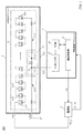
図1は、第1実施形態に係る照明装置100の概略構成図である。
<1.1: Configuration of lighting device>
FIG. 1 is a schematic configuration diagram of an
照明装置100は、図1に示すように、照明用モジュール1と、無線通信用モジュール2と、電源部3とを備える。なお、電源部3は、照明用モジュール1に含まれるものであってもよい。
As illustrated in FIG. 1, the
照明用モジュール1は、第1回路部11と、第2回路部12とを備える。
The
第1回路部11は、図1に示すように、n個(n:自然数)の発光素子(例えば、発光ダイオード(LED))LE1〜LEnと、コイルL2と、コイルL3とを備える。以下では、説明便宜のために、一例として、発光素子が発光ダイオードであるものとして説明する。
As illustrated in FIG. 1, the
n個の発光ダイオードLE1〜LEnは、図1に示すように、アノードが、直流電源供給端子であるVdc端子側となるように、直列に接続されている。 As shown in FIG. 1, the n light emitting diodes LE <b> 1 to LEn are connected in series so that the anode is on the Vdc terminal side which is a DC power supply terminal.
コイルL2の一端は、図1に示すように、発光ダイオードLEnのカソードに接続されおり、コイルL2の他端は、第2回路部12の第1コイルL1の一端および第1コンデンサC1の一端に接続されている。
As shown in FIG. 1, one end of the coil L2 is connected to the cathode of the light emitting diode LEn, and the other end of the coil L2 is connected to one end of the first coil L1 and one end of the first capacitor C1 of the
コイルL3の一端は、図1に示すように、第2回路部12の第1コイルL1のb点側の端部および第2コンデンサC2のb点側の端部に接続されている。コイルL3の他端は、図1に示すように、GND(GND用端子)に接続されている。
As shown in FIG. 1, one end of the coil L3 is connected to the end on the b point side of the first coil L1 of the
第2回路部12は、図1に示すように、第1コイルL1と、第1コンデンサC1と、第2コンデンサC2とを備える。
As shown in FIG. 1, the
第1コイルL1のa点側の端部は、図1に示すように、コイルL2の一端および第1コンデンサのa点側の端部に接続されている。第1コイルL1のb点側の端部は、図1に示すように、コイルL3の一端および第2コンデンサのb点側の端部に接続されている。 As shown in FIG. 1, the end of the first coil L1 on the point a side is connected to one end of the coil L2 and the end of the first capacitor on the point a side. As shown in FIG. 1, the end of the first coil L1 on the point b side is connected to one end of the coil L3 and the end of the second capacitor on the point b side.
第1コンデンサC1は、図1に示すように、一端(a点側の端部)がコイルL1のa点側の端部およびコイルL2の一端に接続されており、他端が無線通信用モジュール2との接続用端子T11と接続されている。 As shown in FIG. 1, the first capacitor C1 has one end (end on the point a side) connected to the end on the point a side of the coil L1 and one end of the coil L2, and the other end is a module for wireless communication. 2 is connected to a connection terminal T11.
第2コンデンサC2は、図1に示すように、一端(b点側の端部)がコイルL1のb点側の端部およびコイルL3の一端に接続されており、他端が無線通信用モジュール2との接続用端子T12と接続されている。 As shown in FIG. 1, the second capacitor C2 has one end (end on the b point side) connected to the end on the b point side of the coil L1 and one end of the coil L3, and the other end is a module for wireless communication. 2 is connected to a connection terminal T12.
また、第1回路部11および第2回路部12は、図1にA11で示した部分(導体パターン)が第1アンテナ部A11を形成し、図1にA12で示した部分(導体パターン)が第2アンテナ部A12を形成するように、構成される。
Further, in the
図2に、第1回路部11および第2回路部12における、第1アンテナ部A11、第2アンテナ部A12、コイルL2、コイルL3、第1コイルL1、第1コンデンサC1、および、第2コンデンサC2の物理構成の一例(概略構成例)を示す。
FIG. 2 shows the first antenna unit A11, the second antenna unit A12, the coil L2, the coil L3, the first coil L1, the first capacitor C1, and the second capacitor in the
第1アンテナ部A11は、照明用モジュール1において、電子部品を実装するためのプリント基板(不図示)上に、細長い矩形状の導体パターン(例えば、銅箔等の金属箔)を形成することで、構成される。第1アンテナ部A11は、例えば、図2に示すように、長手方向の長さd1の細長い矩形状の導体パターンとして形成される。
In the
第2アンテナ部A12は、照明用モジュール1において、電子部品を実装するためのプリント基板(不図示)上に、細長い矩形状の導体パターン(例えば、銅箔等の金属箔)を形成することで、構成される。第2アンテナ部A12は、例えば、図2に示すように、長手方向の長さd2の細長い矩形状の導体パターンとして形成される。
In the
照明用モジュール1において、第1アンテナ部A11および第2アンテナ部A12を半波長ダイポールアンテナとして機能させる場合、第1アンテナ部A11の導体パターンの長手方向の長さd1と、第2アンテナ部A12の導体パターンの長手方向の長さd2は、以下の関係を満たすように決定されることが好ましい。
In the
すなわち、第1アンテナ部A11および第2アンテナ部A12を半波長ダイポールアンテナとして機能させる場合、第1アンテナ部A11および第2アンテナ部A12の導体パターンの周辺の物質(例えば、プリント基板を構成する物質)の比誘電率をεrとし、照明装置100においてアンテナ送受信しようとする電磁波の波長をλとすると、
λ0=λ/sqrt(εr)
d1+d2=λ0/2
sqrt(x):xの平方根を取得する関数
を満たすように、第1アンテナ部A11および第2アンテナ部A12の導体パターンを形成することが好ましい。
That is, when the first antenna unit A11 and the second antenna unit A12 function as a half-wave dipole antenna, a material around the conductor pattern of the first antenna unit A11 and the second antenna unit A12 (for example, a material constituting a printed board) ) Is the dielectric constant εr, and the wavelength of the electromagnetic wave to be transmitted / received to the antenna in the
λ0 = λ / sqrt (εr)
d1 + d2 = λ0 / 2
sqrt (x): The conductor patterns of the first antenna part A11 and the second antenna part A12 are preferably formed so as to satisfy a function for obtaining the square root of x.
また、照明用モジュール1において、第1アンテナ部A11および第2アンテナ部A12を全波長ダイポールアンテナとして機能させる場合、第1アンテナ部A11の導体パターンの長手方向の長さd1と、第2アンテナ部A12の導体パターンの長手方向の長さd2は、以下の関係を満たすように決定されることが好ましい。
Further, in the
すなわち、第1アンテナ部A11および第2アンテナ部A12を全波長ダイポールアンテナとして機能させる場合、第1アンテナ部A11および第2アンテナ部A12の導体パターンの周辺の物質(例えば、プリント基板を構成する物質)の比誘電率をεrとし、照明装置100においてアンテナ送受信しようとする電磁波の波長をλとすると、
λ0=λ/sqrt(εr)
d1+d2=λ0
sqrt(x):xの平方根を取得する関数
を満たすように、第1アンテナ部A11および第2アンテナ部A12の導体パターンを形成することが好ましい。
That is, when the first antenna unit A11 and the second antenna unit A12 function as full-wave dipole antennas, a material around the conductor pattern of the first antenna unit A11 and the second antenna unit A12 (for example, a material constituting a printed board) ) Is the dielectric constant εr, and the wavelength of the electromagnetic wave to be transmitted / received to the antenna in the
λ0 = λ / sqrt (εr)
d1 + d2 = λ0
sqrt (x): The conductor patterns of the first antenna part A11 and the second antenna part A12 are preferably formed so as to satisfy a function for obtaining the square root of x.
なお、第1アンテナ部A11の一端に接続される第1コイルL1および第1コンデンサC1は、プリント基板上の被覆されたパターンや導線(線材)を介して、第1アンテナ部A11の一端に接続されるものであってもよい。また、第1アンテナ部A11の他端に接続されるコイルL2は、プリント基板上の被覆されたパターンや導線(線材)を介して、第1アンテナ部A11の他端に接続されるものであってもよい。 The first coil L1 and the first capacitor C1 connected to one end of the first antenna unit A11 are connected to one end of the first antenna unit A11 through a coated pattern or a conductive wire (wire) on the printed circuit board. It may be done. The coil L2 connected to the other end of the first antenna part A11 is connected to the other end of the first antenna part A11 via a coated pattern or a conductive wire (wire) on the printed circuit board. May be.
また、第2アンテナ部A12の一端に接続される第1コイルL1および第2コンデンサC2は、プリント基板上の被覆されたパターンや導線(線材)を介して、第2アンテナ部A12の一端に接続されるものであってもよい。また、第2アンテナ部A12の他端に接続されるコイルL3は、プリント基板上の被覆されたパターンや導線(線材)を介して、第2アンテナ部A12の他端に接続されるものであってもよい。 Also, the first coil L1 and the second capacitor C2 connected to one end of the second antenna part A12 are connected to one end of the second antenna part A12 via a coated pattern or a conductive wire (wire) on the printed circuit board. It may be done. The coil L3 connected to the other end of the second antenna portion A12 is connected to the other end of the second antenna portion A12 via a coated pattern or a conductive wire (wire) on the printed circuit board. May be.
無線通信用モジュール2は、図1に示すように、マッチング部21と、RF部22と、通信制御部23とを備える。
As shown in FIG. 1, the
マッチング部21は、インピーダンス調整を行う回路(インピーダンス調整回路)等を備える。マッチング部21のインピーダンス調整回路は、照明用モジュール1と無線通信用モジュール2との接続用端子T11、T12を介して、照明用モジュール1の第2回路部12と接続され、インピーダンス調整を行う。照明用モジュール1を送受信アンテナとして機能させる場合、マッチング部21は、送信用インピーダンス調整回路と、受信用インピーダンス調整回路とを備えてもよい。なお、照明用モジュール1を送受信アンテナとして機能させる場合、マッチング部21は、送信用インピーダンス調整回路と、受信用インピーダンス調整回路とを共通化した回路を備えるものであってもよい。
The matching
マッチング部21は、照明用モジュール1が受信アンテナとして機能している場合、インピーダンス調整後の信号をRF部22に出力する。一方、マッチング部21は、照明用モジュール1が送信アンテナとして機能している場合、RF部22からの信号を入力し、入力された信号に対してインピーダンス調整を行い、インピーダンス調整後の信号を、接続用端子T11、T12を介して、照明用モジュール1の第2回路部12に出力する。
The matching
RF部22は、アンテナ送信処理部(例えば、アンテナ送信処理用回路)と、アンテナ受信処理部(例えば、アンテナ受信処理用回路)と、備える。RF部22は、通信制御部23からの指令信号(制御信号)を入力し、当該指令信号(制御信号)に基づいた処理を実行する。
The
RF部22は、照明用モジュール1が受信アンテナとして機能している場合、アンテナ受信処理部(例えば、アンテナ受信処理用回路)を動作させ、マッチング部21から出力されるインピーダンス調整後の信号に対して、アンテナ受信処理(例えば、RF復調処理を含む処理)を実行する。そして、RF部22は、アンテナ受信処理(例えば、RF復調処理)により取得した信号(情報)を通信制御部23に出力する。
When the
一方、RF部22は、照明用モジュール1が送信アンテナとして機能している場合、アンテナ送信処理部(例えば、アンテナ送信処理用回路)を動作させる。例えば、通信制御部23から出力される信号(情報)をRF変調し、RF変調した信号をマッチング部21に出力する。
On the other hand, when the
通信制御部23は、無線通信用モジュール2の各機能部を制御する。通信制御部23は、例えば、マイクロプロセッサ等により実現される。通信制御部23は、RF部22と接続されており、RF部22に制御信号、RF変調させてアンテナ送信するための情報(信号)等を出力する。
The
また、通信制御部23は、RF部22からの信号により、自装置以外の他の照明装置から電波が送信されている状態であることを検出した場合、混信、コリジョン発生等を防止するために、自装置のRF変調処理を停止させるための制御信号をRF部22に出力するようにしてもよい。
In addition, when the
また、通信制御部23は、RF部22からの信号に基づいて、電源制御信号Ctlを生成し、生成した電源制御信号Ctlを電源部3に出力する。
Further, the
なお、無線通信用モジュール2は、照明用モジュール1とコネクタ等により脱着可能に接続されるものであってもよい。また、無線通信用モジュール2は、電源部3とコネクタ等により脱着可能に接続されるものであってもよい。
The
電源部3は、交流電源(不図示)に接続され、交流電流(あるいは交流電圧)を直流電流(あるいは直流電圧)に変換することで、外部に対して、定電圧源として機能する。電源部3は、無線通信用モジュール2に接続され、無線通信用モジュール2に対して、定電圧DC_Wを供給する直流電源として機能する。
The
また、電源部3は、照明用モジュール1の直流電源供給端子であるVdc端子(およびGND端子)を介して、照明用モジュール1と接続され、照明用モジュール1に対して、電圧DC_Lを供給する直流電源として機能する。
The
また、電源部3は、通信制御部23から出力される電源制御信号Ctlを入力する。電源部3は、電源制御信号Ctlに基づいて、照明用モジュール1に供給(出力)する電圧DC_Lの値を調整する。
The
なお、電源部3は、照明用モジュール1とコネクタ等により脱着可能に接続されるものであってもよい。また、電源部3は、無線通信用モジュール2とコネクタ等により脱着可能に接続されるものであってもよい。
The
<1.2:照明装置の動作>
以上のように構成された照明装置100の動作について、以下、説明する。
<1.2: Operation of lighting device>
The operation of the
なお、以下では、搬送波周波数fが920[MHz]である電磁波を送受信するためのアンテナとして、照明装置100を機能させる場合を、一例に、説明する。
Hereinafter, a case where the
まず、第1回路部11のコイルL2およびコイルL3、第2回路部12の第1コイルL1、第1コンデンサC1、および、第2コンデンサC2のインダクタンス値および容量値(キャパシタンス値)を、以下のように設定する。
First, the inductance values and capacitance values (capacitance values) of the coils L2 and L3 of the
L1=L2=L3=100[μH]
C1=C2=10[μF]
なお、第1コイルL1、コイルL2、コイルL3のインダクタンス値を示す変数を、それぞれ、L1、L2、L3と表記する。
L1 = L2 = L3 = 100 [μH]
C1 = C2 = 10 [μF]
The variables indicating the inductance values of the first coil L1, the coil L2, and the coil L3 are denoted as L1, L2, and L3, respectively.
また、第1コンデンサC1、第2コンデンサC2のキャパシタンス値を示す変数を、それぞれ、C1、C2と表記する。
The first capacitor C1, a second variable indicating the capacitance value of the
なお、上記インダクタンス値およびキャパシタンス値は、一例であり、上記の値に限定されない。 In addition, the said inductance value and capacitance value are examples, and are not limited to said value.
上記のようにインダクタンス値およびキャパシタンス値を設定した場合、第1回路部11のコイルL2およびコイルL3、第2回路部12の第1コイルL1、第1コンデンサC1、および、第2コンデンサC2の、周波数f=920[MHz]における誘導リアクタンスXLおよび容量リアクタンスXcは、以下の通りである。
When the inductance value and the capacitance value are set as described above, the coils L2 and L3 of the
XL(L1)=XL(L2)=XL(L3)≒578[kΩ]
Xc(C1)=Xc(C2)≒0.0173[mΩ]
なお、第1コイルL1、コイルL2、コイルL3の誘導リアクタンスXLを、それぞれ、XL(L1)、XL(L2)、XL(L3)と表記する。
XL (L1) = XL (L2) = XL (L3) ≈578 [kΩ]
Xc (C1) = Xc (C2) ≈0.0173 [mΩ]
The inductive reactance XL of the first coil L1, the coil L2, and the coil L3 is expressed as XL (L1), XL (L2), and XL (L3), respectively.
また、第1コンデンサC1、第2コンデンサC2の容量リアクタンスXcを、それぞれ、Xc(C1)、Xc(C2)と表記する。 Further, the capacitive reactances Xc of the first capacitor C1 and the second capacitor C2 are denoted as Xc (C1) and Xc (C2), respectively.
上記から分かるように、周波数f=920[MHz]において、誘導リアクタンスXLは、十分高いインピーダンスであり、容量リアクタンスXcは、十分低いインピーダンスである。 As can be seen from the above, at the frequency f = 920 [MHz], the inductive reactance XL has a sufficiently high impedance, and the capacitive reactance Xc has a sufficiently low impedance.
一方、直流、すなわち、周波数f=0[Hz]において、誘導リアクタンスXLは、「0Ω」であり、容量リアクタンスXcは、無限大である。 On the other hand, at direct current, that is, at a frequency f = 0 [Hz], the inductive reactance XL is “0Ω”, and the capacitive reactance Xc is infinite.
上記のように、第1回路部11のコイルL2およびコイルL3、第2回路部12の第1コイルL1、第1コンデンサC1、および、第2コンデンサC2のインダクタンス値および容量値(キャパシタンス値)を、設定することで、照明装置100では、照明制御機能と、アンテナ機能との両方の機能を実現することができる。
As described above, the inductance value and the capacitance value (capacitance value) of the coils L2 and L3 of the
これについて、図3〜図6を用いて、説明する。 This will be described with reference to FIGS.
まず、照明制御機能について説明する。 First, the illumination control function will be described.
図3は、照明用モジュール1に対して、接続用端子T11、T12間に、周波数f=920[MHz]の交流信号源を接続し、直流電源供給端子であるVdc端子とGND端子との間に電圧DC_Lを供給する直流電源とを接続した場合を示している。
FIG. 3 shows an
直流成分の信号(周波数f=0[Hz]の信号)に対して、誘導リアクタンスXLは、「0Ω」であり、容量リアクタンスXcは、無限大であるので、直流成分の信号(周波数f=0[Hz]の信号)について、図3に示す回路は、図4に示す回路と等価となる。 With respect to a DC component signal (frequency f = 0 [Hz] signal), the inductive reactance XL is “0Ω”, and the capacitive reactance Xc is infinite, so the DC component signal (frequency f = 0). For [Hz] signal), the circuit shown in FIG. 3 is equivalent to the circuit shown in FIG.
つまり、図4から分かるように、直流成分の信号(周波数f=0[Hz]の信号)に対して、照明装置100の照明用モジュール1は、照明制御機能を実現する回路を構成する。すなわち、図4に示すように、Vdc端子とGND端子との間にかけられた電圧DC_Lにより、n個の発光素子LE1〜LEnに順方向バイアスがかかり、n個の発光素子LE1〜LEnが発光する。これにより、照明装置100では、照明制御機能を実現することができる。なお、Vdc端子とGND端子との間にかける電圧DC_Lの電圧値を調整することで、n個の発光素子LE1〜LEnの発光量を調整することができる。
That is, as can be seen from FIG. 4, the
次に、アンテナ機能について説明する。 Next, the antenna function will be described.
L1=L2=L3=100[μH]
C1=C2=10[μF]
である場合、
XL(L1)=XL(L2)=XL(L3)≒578[kΩ]
Xc(C1)=Xc(C2)≒0.0173[mΩ]
であるので、周波数f=920[MHz]の信号に対して、第1コイルL1、コイルL2、および、コイルL3の誘導リアクタンスXLは、十分高いインピーダンス(約578[kΩ])であり、近似的に、電気的に接続されていない状態とみなすことができる。
L1 = L2 = L3 = 100 [μH]
C1 = C2 = 10 [μF]
If it is,
XL (L1) = XL (L2) = XL (L3) ≈578 [kΩ]
Xc (C1) = Xc (C2) ≈0.0173 [mΩ]
Therefore, for the signal of frequency f = 920 [MHz], the inductive reactance XL of the first coil L1, the coil L2, and the coil L3 has a sufficiently high impedance (about 578 [kΩ]), which is approximately In addition, it can be regarded as a state where they are not electrically connected.
一方、周波数f=920[MHz]の信号に対して、第1コンデンサC1および第2コンデンサC2の容量リアクタンスXcは、十分低いインピーダンス(約0.0173[mΩ])であり、近似的に、直結されている状態とみなすことができる。 On the other hand, the capacitive reactance Xc of the first capacitor C1 and the second capacitor C2 has a sufficiently low impedance (about 0.0173 [mΩ]) with respect to a signal of frequency f = 920 [MHz], and is approximately directly coupled. It can be regarded as being in a state.
したがって、周波数f=920[MHz]の信号に対して、図3に示す回路は、図5に示す回路と近似的に等価とみなすことができる。つまり、この場合、図3に示す回路は、図6に示す回路と近似的に等価とみなすことができる。図6から分かるように、周波数f=920[MHz]の信号に対して、照明装置100の照明用モジュール1は、第1アンテナ部A11および第2アンテナ部A12をアンテナ素子とするダイポールアンテナと略同様の機能を実現することができる。
Therefore, the circuit shown in FIG. 3 can be regarded as approximately equivalent to the circuit shown in FIG. 5 for a signal of frequency f = 920 [MHz]. That is, in this case, the circuit shown in FIG. 3 can be regarded as approximately equivalent to the circuit shown in FIG. As can be seen from FIG. 6, the
このように、照明装置100の照明用モジュール1の回路は、直流成分の信号に対しては、照明制御機能を実現する回路として機能し、高周波成分の信号(例えば、周波数f=920[MHz]の信号)に対しては、アンテナ機能を実現する回路として機能する。
As described above, the circuit of the
次に、照明装置100の具体的動作について、一例を挙げて、以下、説明する。
Next, a specific operation of the
具体的には、照明装置100において、n個の発光素子LE1〜LEnの全てが消灯している状態(初期状態)において、
(1)外部から無線通信により、照明装置100の照明用モジュール1のn個の発光素子LE1〜LEnを点灯させるよう指示する情報を含む無線信号(電磁波)を、照明装置100が、受信し(アンテナ受信処理)、
(2)受信した無線信号に含まれる指示情報に従い、照明装置100が、照明用モジュール1のn個の発光素子LE1〜LEnを点灯させる制御を行い(照明制御処理)、
(3)照明装置100が、照明用モジュール1のn個の発光素子LE1〜LEnを点灯させた状態であることを示す情報と、当該状態における消費電力を示す情報とを無線信号(電磁波)により、照明装置100から外部へ送信する(アンテナ送信処理)、
場合について、照明装置100の具体的動作を、以下、説明する。
Specifically, in the
(1) The illuminating
(2) In accordance with the instruction information included in the received wireless signal, the
(3) Information indicating that the
A specific operation of the
なお、照明装置100の第1回路部11のコイルL2およびコイルL3、第2回路部12の第1コイルL1、第1コンデンサC1、および、第2コンデンサC2のインダクタンス値およびキャパシタンス値は、
L1=L2=L3=100[μH]
C1=C2=10[μF]
に設定されており、アンテナ送受信する無線信号の搬送周波数は、920[MHz]であるものとする。
The inductance value and the capacitance value of the coil L2 and the coil L3 of the
L1 = L2 = L3 = 100 [μH]
C1 = C2 = 10 [μF]
It is assumed that the carrier frequency of the radio signal transmitted and received by the antenna is 920 [MHz].
(1.2.1:アンテナ受信処理)
照明装置100は、搬送周波数が920[MHz]であり、照明装置100の照明用モジュール1のn個の発光素子LE1〜LEnを点灯させるよう指示する情報を含む無線信号(当該情報を示す信号を、搬送周波数920[MHz]の搬送波信号を用いて変調した無線信号)を、第1アンテナ部A11および第2アンテナ部A12により受信する。
(1.2.1: Antenna reception processing)
The illuminating
なお、照明装置100では、上記で説明したように、周波数が約920[MHz]の無線信号に対するアンテナ感度が高くなるように、第1アンテナ部A11の導体パターンの長手方向の長さd1と、第2アンテナ部A12の導体パターンの長手方向の長さd2とが設定されている。以下では、説明便宜のため、照明用モジュール1において、第1アンテナ部A11および第2アンテナ部A12が、半波長ダイポールアンテナとして機能するものとする。
In the
つまり、第1アンテナ部A11および第2アンテナ部A12の導体パターンの周辺の物質(例えば、プリント基板を構成する物質)の比誘電率をεrとし、照明装置100においてアンテナ送受信しようとする電磁波の波長(920[MHz]の電磁波に相当する波長)をλとすると、
λ0=λ/sqrt(εr)
d1+d2=λ0/2
sqrt(x):xの平方根を取得する関数
を満たすように、第1アンテナ部A11および第2アンテナ部A12の導体パターンを形成されているものとする。
That is, the relative dielectric constant of the material around the conductor pattern of the first antenna unit A11 and the second antenna unit A12 (for example, the material constituting the printed circuit board) is εr, and the wavelength of the electromagnetic wave to be transmitted / received to the antenna in the
λ0 = λ / sqrt (εr)
d1 + d2 = λ0 / 2
sqrt (x): It is assumed that the conductor patterns of the first antenna unit A11 and the second antenna unit A12 are formed so as to satisfy the function for obtaining the square root of x.
第1アンテナ部A11および第2アンテナ部A12により受信された無線信号は、無線通信用モジュール2のマッチング部21に入力される。
The radio signals received by the first antenna unit A11 and the second antenna unit A12 are input to the
マッチング部21に入力された無線信号は、マッチング部21において、インピーダンス調整処理が実行され、インピーダンス調整処理後の信号が、RF部に出力される。
The wireless signal input to the
RF部では、マッチング部21から出力された信号に対して、RF信号処理(例えば、RF復調処理等)が実行され、無線信号に含まれる情報(照明装置100の照明用モジュール1のn個の発光素子LE1〜LEnを点灯させるよう指示する情報)が取得される。
In the RF unit, RF signal processing (for example, RF demodulation processing or the like) is performed on the signal output from the matching
RF部22により取得された情報は、通信制御部23に出力される。
Information acquired by the
(1.2.2:照明制御処理)
通信制御部23では、RF部22から出力された情報(照明装置100の照明用モジュール1のn個の発光素子LE1〜LEnを点灯させるよう指示する情報)に基づいて、照明用モジュール1に電圧値DC_Lの直流電圧をかけるように制御するための制御信号Ctlを電源部3に出力する。
(1.2.2: Lighting control processing)
In the
電源部3は、無線通信用モジュール2の通信制御部23から出力される制御信号Ctlに基づいて、照明用モジュール1に電圧値DC_Lの直流電圧をかける。
The
これにより、照明用モジュール1の直流電源供給端子であるVdc端子とGND端子との間に電圧値DC_Lの直流電圧がかかる。第1コイルL1、コイルL2、および、コイルL3は、直流成分に対するインピーダンス(誘導リアクタンス)は、0Ωであるので、Vdc端子とGND端子との間に電圧値DC_Lの直流電圧がかかることで、n個の発光素子LE1〜LEnに順方向バイアスがかかり、直流電流が流れ、n個の発光素子LE1〜LEnは、発光する。すなわち、照明装置100は、n個の発光素子LE1〜LEnを点灯させる。
As a result, a DC voltage having a voltage value DC_L is applied between the Vdc terminal, which is a DC power supply terminal of the
(1.2.3:アンテナ送信処理)
無線通信用モジュール2の通信制御部23は、上記照明制御処理を行うとともに、照明装置100が、照明用モジュール1のn個の発光素子LE1〜LEnを点灯させた状態であることを示す情報と、当該状態における消費電力を示す情報とを生成し、生成した情報をRF部22に出力する。
(1.2.3: Antenna transmission processing)
The
RF部22では、通信制御部23から出力された情報を、搬送周波数920[MHz]の搬送波信号を用いてRF変調することで、通信制御部23から出力された情報を含む無線信号を生成する。そして、RF部22は、生成した無線信号をマッチング部21に出力する。
The
マッチング部21では、RF部22から出力された無線信号に対して、インピーダンス調整処理を行い、インピーダンス調整後の無線信号を、照明用モジュール1の第2回路部12に出力する。
The matching
照明用モジュール1の回路は、上記で説明したように、周波数920[MHz]の高周波信号に対しては、ダイポールアンテナとして機能する。したがって、無線通信用モジュール2から出力された無線信号は、照明用モジュール1の第1アンテナ部A11および第2アンテナ部A12により、電磁波(無線信号)として、外部に放射される。
As described above, the circuit of the
以上のように、照明装置100では、照明用モジュール1の回路が、(1)直流成分の信号に対して、発光素子を点灯させる回路として機能し、(2)高周波成分の信号に対しては、ダイポールアンテナを構成する回路として機能する。つまり、照明装置100では、1つの回路で、照明用の回路と、無線通信のためのアンテナ用の回路との両方を実現することができる。
As described above, in the
したがって、照明装置100では、無線通信機能を実現させるために、従来のように、照明装置の外部に大きなアンテナを設置する必要がないので、照明機器の外観を損ねることがない。また、内部が空洞の細長い照明用管内に、照明用モジュール1を設置する場合、n個の発光素子を、当該照明用管の長手方向に配置するとともに、第1アンテナ部A11および第2アンテナ部A12の導体パターンを形成する領域を容易に確保することができ、さらに、アンテナ感度が良好となる領域(例えば、照明用管の長手方向の略中央部)に、第1アンテナ部A11および第2アンテナ部A12の導体パターンを形成させることも容易となる。
Therefore, in the
このように、照明装置100では、照明機器の外観を損ねず、照明機器の照明性能を確保し、かつ、信頼性の高い無線通信を実行することができる。
As described above, in the
[第2実施形態]
次に、第2実施形態について、説明する。
[Second Embodiment]
Next, a second embodiment will be described.
なお、本実施形態において、第1実施形態と同様の部分については、同一符号を付し、詳細な説明を省略する。 In the present embodiment, the same parts as those in the first embodiment are denoted by the same reference numerals, and detailed description thereof is omitted.
図7は、第2実施形態の照明装置200の概略構成図である。
FIG. 7 is a schematic configuration diagram of the
第2実施形態の照明装置200は、図7に示すように、第1実施形態の照明装置100において、照明用モジュール1を、照明用モジュール1Aに置換した構成を有している。
As shown in FIG. 7, the
照明用モジュール1Aは、図7に示すように、第1実施形態の照明用モジュール1において、第1回路部11を、第1回路部11Aに置換した構成を有している。
As shown in FIG. 7, the illumination module 1A has a configuration in which the
第1回路部11Aにおいて、図7に示すように、直流電源供給端子であるVdc端子と、図7のc点との間にコイルL4が設置されており、図7のc点とd点の間に、コンデンサC3が設置されている。また、第1回路部11Aにおいて、図7のd点とGND端子との間に、コイルL5が設置されている。
In the
以上のように構成された照明装置200の照明用モジュール1Aの回路は、直流成分の信号に対しては、n個の発光素子LE1〜LEnを点灯させる回路として機能し、高周波成分の信号に対しては、ループアンテナを構成する回路として機能する。
The circuit of the illumination module 1A of the
なお、一例として、照明装置200の第1回路部11AのコイルL4、コイルL5、コンデンサC3、第2回路部12の第1コイルL1、第1コンデンサC1、および、第2コンデンサC2のインダクタンス値およびキャパシタンス値は、
L1=L4=L5=100[μH]
C1=C2=C3=10[μF]
に設定されており、アンテナ送受信する無線信号の搬送周波数は、920[MHz]であるものとする。
As an example, the inductance values of the coil L4, the coil L5, the capacitor C3 of the
L1 = L4 = L5 = 100 [μH]
C1 = C2 = C3 = 10 [μF]
It is assumed that the carrier frequency of the radio signal transmitted and received by the antenna is 920 [MHz].
上記のようにインダクタンス値およびキャパシタンス値を設定した場合、第1回路部11AのコイルL4およびコイルL5、第2回路部12の第1コイルL1、第1コンデンサC1、および、第2コンデンサC2の、周波数f=920[MHz]における誘導リアクタンスXLおよび容量リアクタンスXcは、以下の通りである。
When the inductance value and the capacitance value are set as described above, the coils L4 and L5 of the
XL(L1)=XL(L4)=XL(L5)≒578[kΩ]
Xc(C1)=Xc(C2)=Xc(C3)≒0.0173[mΩ]
なお、第1コイルL1、コイルL4、コイルL5の誘導リアクタンスXLを、それぞれ、XL(L1)、XL(L4)、XL(L5)と表記する。
XL (L1) = XL (L4) = XL (L5) ≈578 [kΩ]
Xc (C1) = Xc (C2) = Xc (C3) ≈0.0173 [mΩ]
The inductive reactance XL of the first coil L1, the coil L4, and the coil L5 is expressed as XL (L1), XL (L4), and XL (L5), respectively.
また、第1コンデンサC1、第2コンデンサC2、コンデンサC3の容量リアクタンスXcを、それぞれ、Xc(C1)、Xc(C2)、Xc(C3)と表記する。 Further, the capacitive reactances Xc of the first capacitor C1, the second capacitor C2, and the capacitor C3 are expressed as Xc (C1), Xc (C2), and Xc (C3), respectively.
上記から分かるように、周波数f=920[MHz]において、誘導リアクタンスXLは、十分高いインピーダンスであり、容量リアクタンスXcは、十分低いインピーダンスである。 As can be seen from the above, at the frequency f = 920 [MHz], the inductive reactance XL has a sufficiently high impedance, and the capacitive reactance Xc has a sufficiently low impedance.
一方、直流、すなわち、周波数f=0[Hz]において、誘導リアクタンスXLは、「0Ω」であり、容量リアクタンスXcは、無限大である。 On the other hand, at direct current, that is, at a frequency f = 0 [Hz], the inductive reactance XL is “0Ω”, and the capacitive reactance Xc is infinite.
上記のように、第1回路部11AのコイルL4、コイルL5、コンデンサC3、第2回路部12の第1コイルL1、第1コンデンサC1、および、第2コンデンサC2のインダクタンス値および容量値(キャパシタンス値)を、設定することで、照明装置200では、照明制御機能と、アンテナ機能との両方の機能を実現することができる。
As described above, the inductance value and the capacitance value (capacitance value) of the coil L4, the coil L5, the capacitor C3 of the
これについて、図8〜図10を用いて、説明する。 This will be described with reference to FIGS.
まず、照明制御機能について説明する。 First, the illumination control function will be described.
図8は、照明用モジュール1Aに対して、接続用端子T11、T12間に、周波数f=920[MHz]の交流信号源を接続し、直流電源供給端子であるVdc端子とGND端子との間に電圧DC_Lを供給する直流電源とを接続した場合を示している。 FIG. 8 shows that an AC signal source having a frequency f = 920 [MHz] is connected between the connection terminals T11 and T12 to the illumination module 1A, and between the Vdc terminal and the GND terminal which are DC power supply terminals. The figure shows a case where a direct current power source that supplies a voltage DC_L is connected to.
直流成分の信号(周波数f=0[Hz]の信号)に対して、誘導リアクタンスXLは、「0Ω」であり、容量リアクタンスXcは、無限大であるので、直流成分の信号(周波数f=0[Hz]の信号)について、図8に示す回路は、図9に示す回路と等価となる。 With respect to a DC component signal (frequency f = 0 [Hz] signal), the inductive reactance XL is “0Ω”, and the capacitive reactance Xc is infinite, so the DC component signal (frequency f = 0). For the signal [Hz], the circuit shown in FIG. 8 is equivalent to the circuit shown in FIG.
つまり、図9から分かるように、直流成分の信号(周波数f=0[Hz]の信号)に対して、照明装置200の照明用モジュール1Aは、照明制御機能を実現する回路を構成する。すなわち、図9に示すように、Vdc端子とGND端子との間にかけられた電圧DC_Lにより、n個の発光素子LE1〜LEnに順方向バイアスがかかり、n個の発光素子LE1〜LEnが発光する。これにより、照明装置200では、照明制御機能を実現することができる。なお、Vdc端子とGND端子との間にかける電圧DC_Lの電圧値を調整することで、n個の発光素子LE1〜LEnの発光量を調整することができる。
That is, as can be seen from FIG. 9, the
次に、アンテナ機能について説明する。 Next, the antenna function will be described.
L1=L4=L5=100[μH]
C1=C2=C3=10[μF]
である場合、
XL(L1)=XL(L4)=XL(L5)≒578[kΩ]
Xc(C1)=Xc(C2)=Xc(C3)≒0.0173[mΩ]
であるので、周波数f=920[MHz]の信号に対して、第1コイルL1、コイルL4、および、コイルL5の誘導リアクタンスXLは、十分高いインピーダンス(約578[kΩ])であり、近似的に、電気的に接続されていない状態とみなすことができる。
L1 = L4 = L5 = 100 [μH]
C1 = C2 = C3 = 10 [μF]
If it is,
XL (L1) = XL (L4) = XL (L5) ≈578 [kΩ]
Xc (C1) = Xc (C2) = Xc (C3) ≈0.0173 [mΩ]
Therefore, the inductive reactance XL of the first coil L1, the coil L4, and the coil L5 has a sufficiently high impedance (about 578 [kΩ]) with respect to a signal having a frequency f = 920 [MHz], which is approximately In addition, it can be regarded as a state where they are not electrically connected.
一方、周波数f=920[MHz]の信号に対して、第1コンデンサC1、第2コンデンサC2、および、コンデンサC3の容量リアクタンスXcは、十分低いインピーダンス(約0.0173[mΩ])であり、近似的に、直結されている状態とみなすことができる。 On the other hand, the capacitive reactance Xc of the first capacitor C1, the second capacitor C2, and the capacitor C3 has a sufficiently low impedance (about 0.0173 [mΩ]) with respect to a signal having a frequency f = 920 [MHz]. Approximately, it can be regarded as a directly connected state.
したがって、周波数f=920[MHz]の信号に対して、図8に示す回路は、図10に示す回路と近似的に等価とみなすことができる。つまり、この場合、図8に示す回路は、図10から分かるように、点b、点d、点c、点aにより形成されるパスが、ループアンテナを構成する。このループアンテナを構成する部分について、例えば、照明用モジュール1Aのプリント基板上に導体パターン(例えば、銅箔等の金属箔)を形成させることで、ループアンテナを構成させるようにすることが好ましい。 Therefore, the circuit shown in FIG. 8 can be regarded as approximately equivalent to the circuit shown in FIG. 10 for a signal having a frequency f = 920 [MHz]. That is, in this case, as can be seen from FIG. 10, in the circuit shown in FIG. 8, the path formed by the points b, d, c, and a constitutes a loop antenna. As for the portion constituting the loop antenna, for example, it is preferable to form a loop antenna by forming a conductor pattern (for example, a metal foil such as a copper foil) on the printed board of the illumination module 1A.
また、点b、点d、点c、点aにより形成されるループアンテナのパスの長さをd3とし、照明装置200で送受信する無線信号(電磁波)の波長をλとし、照明用モジュール1Aのループアンテナを構成する導体パターンの周辺の物質(例えば、プリント基板を構成する物質)の比誘電率をεrとすると、
λ0=λ/sqrt(εr)
d3=λ0
sqrt(x):xの平方根を取得する関数
を満たすように、照明装置200において、ループアンテナを構成する導体パターンを形成するのが好ましい。
In addition, the length of the path of the loop antenna formed by the points b, d, c, and a is d3, the wavelength of the radio signal (electromagnetic wave) transmitted and received by the
λ0 = λ / sqrt (εr)
d3 = λ0
sqrt (x): It is preferable to form a conductor pattern constituting the loop antenna in
このように構成することで、周波数f=920[MHz]の信号に対して、照明装置200の照明用モジュール1Aは、点b、点d、点c、点aにより形成されるパスをアンテナ素子とするループアンテナと略同様の機能を実現することができる。
With this configuration, the
このように、照明装置200の照明用モジュール1Aの回路は、直流成分の信号に対しては、照明制御機能を実現する回路として機能し、高周波成分の信号(例えば、周波数f=920[MHz]の信号)に対しては、アンテナ機能を実現する回路として機能する。
As described above, the circuit of the illumination module 1A of the
なお、照明装置200Aの具体的な動作は、第1実施形態の照明装置100と同様であるので、詳細な説明を省略する。
The specific operation of the lighting device 200A is the same as that of the
以上のように、照明装置200では、照明用モジュール1の回路が、(1)直流成分の信号に対して、発光素子を点灯させる回路として機能し、(2)高周波成分の信号に対しては、ループアンテナを構成する回路として機能する。つまり、照明装置200では、1つの回路で、照明用の回路と、無線通信のためのアンテナ用の回路との両方を実現することができる。
As described above, in the
したがって、照明装置200では、無線通信機能を実現させるために、従来のように、照明装置の外部に大きなアンテナを設置する必要がないので、照明機器の外観を損ねることがない。また、内部が空洞の細長い照明用管内に、照明用モジュール1Aを設置する場合、n個の発光素子を、当該照明用管の長手方向に配置するとともに、ループアンテナの導体パターン(の一部)を形成する領域を容易に確保することができ、さらに、アンテナ感度が良好となる領域(例えば、照明用管の長手方向の略中央部)に、ループアンテナの導体パターン(の一部)を形成させることも容易となる。
Therefore, in the
このように、照明装置200では、照明機器の外観を損ねず、照明機器の照明性能を確保し、かつ、信頼性の高い無線通信を実行することができる。
Thus, in the
[第3実施形態]
次に、第3実施形態について、説明する。
[Third embodiment]
Next, a third embodiment will be described.
なお、本実施形態において、上記実施形態と同様の部分については、同一符号を付し、詳細な説明を省略する。 In the present embodiment, the same parts as those in the above embodiment are denoted by the same reference numerals, and detailed description thereof is omitted.
図11は、第3実施形態に係る照明制御システム3000の概略構成図である。
FIG. 11 is a schematic configuration diagram of an
照明制御システム3000は、図11に示すように、ネットワークN1(有線ネットワークN1)に接続されたマスター装置M1と、第1スレーブ装置S1と、第2スレーブ装置S2と、第3スレーブ装置S3とを備える。ネットワークN1は、例えば、専用線による有線ネットワークや、電力線に信号を変調して重畳させて通信するネットワーク(例えば、電力線搬送通信ネットワーク(PLCネットワーク))等である。
As shown in FIG. 11, the
また、照明制御システム3000は、図11に示すように、第1スレーブ装置S1に無線通信ネットワークW1により接続される脱着式無線通信用モジュールWM11と、脱着式無線通信用モジュールWM12に接続されている照明用モジュールLM12とを備える。
As shown in FIG. 11, the
また、照明制御システム3000は、図11に示すように、第2スレーブ装置S2に無線通信ネットワークW2により接続される脱着式無線通信用モジュールWM21と、脱着式無線通信用モジュールWM22に接続されている照明用モジュールLM22とを備える。
Further, as shown in FIG. 11, the
また、照明制御システム3000は、図11に示すように、第3スレーブ装置S3に無線通信ネットワークW3により接続される照度センサSS31と、人感センサSS32とを備える。
Moreover, as shown in FIG. 11, the
なお、図11の場合、照明制御システム3000は、1つのマスター装置と、3つのスレーブ装置とを備えているが、照明制御システム3000は、この構成に限定されることはなく、複数のマスター装置と、複数のスレーブ装置とを備えるものであってもよい。
In the case of FIG. 11, the
脱着式無線通信用モジュールWM11、WM12、WM21、WM22は、上記実施形態で説明した無線通信用モジュール2と同様のものであり、コネクタ等により、照明用モジュールと脱着可能である。
The removable wireless communication modules WM11, WM12, WM21, and WM22 are the same as the
照明用モジュールLM11、LM12、LM21、LM22は、上記実施形態で説明した照明用モジュール1または1Aと同様のものである。なお、電源部3については、図示を省略している。
The illumination modules LM11, LM12, LM21, and LM22 are the same as the
例えば、照明制御システム3000において、照度センサSS31により検出されている照度が低い(暗い)状態であり、人感センサSS32により、人を検知し、消灯している照明用モジュールLM11の複数の発光素子を点灯させる場合の制御について、以下、説明する。
For example, in the
まず、照度センサSS31は、照度センサSS31により検出されている照度が低い(暗い)ことを示す情報を含む信号を、無線通信ネットワークW3を介して、第3スレーブ装置S3に送信する。 First, the illuminance sensor SS31 transmits a signal including information indicating that the illuminance detected by the illuminance sensor SS31 is low (dark) to the third slave device S3 via the wireless communication network W3.
第3スレーブ装置S3は、無線通信ネットワークW3を介して、照度センサSS31から取得した情報を含む信号を、有線ネットワークN1を介して、マスター装置M1に送信する。 The third slave device S3 transmits a signal including information acquired from the illuminance sensor SS31 via the wireless communication network W3 to the master device M1 via the wired network N1.
マスター装置M1は、第3スレーブ装置S3から、有線ネットワークN1を介して受信した照度センサSS31が検知した照度についての情報を取得し、当該情報を保持する。 The master device M1 acquires information about the illuminance detected by the illuminance sensor SS31 received via the wired network N1 from the third slave device S3, and holds the information.
次に、人感センサSS32が、人を検知すると、人感センサSS32は、人を感知したことを示す情報を含む信号を、無線通信ネットワークW3を介して、第3スレーブ装置S3に送信する。 Next, when the human sensor SS32 detects a person, the human sensor SS32 transmits a signal including information indicating that the person is detected to the third slave device S3 via the wireless communication network W3.
第3スレーブ装置S3は、人感センサSS32から、無線通信ネットワークW3を介して受信した情報(人を検知したことを示す情報)を、有線ネットワークN1を介して、マスター装置M1に送信する。 The third slave device S3 transmits information received from the human sensor SS32 via the wireless communication network W3 (information indicating that a person has been detected) to the master device M1 via the wired network N1.
マスター装置M1は、第3スレーブ装置S3から、有線ネットワークN1を介して受信した信号により、人感センサSS32により、人が検知されたという情報を取得する。そして、マスター装置M1は、照明用モジュールLM11の複数の発光素子の点灯を指示する信号を、有線ネットワークN1を介して、第1スレーブ装置S1に送信する。 The master device M1 acquires information indicating that a person has been detected by the human sensor SS32 based on a signal received from the third slave device S3 via the wired network N1. And the master apparatus M1 transmits the signal which instruct | indicates lighting of the several light emitting element of module LM11 for illumination to 1st slave apparatus S1 via the wired network N1.
第1スレーブ装置S1は、マスター装置M1から、有線ネットワークN1を介して送信された信号を受信し、受信した信号を、無線通信ネットワークW1を介して、脱着式無線通信用モジュールWM11に送信する。 The first slave device S1 receives a signal transmitted from the master device M1 via the wired network N1, and transmits the received signal to the removable wireless communication module WM11 via the wireless communication network W1.
脱着式無線通信用モジュールWM11は、第1スレーブ装置S1からの信号を、無線通信ネットワークW1を介して受信する。具体的には、第1スレーブ装置S1からの無線信号を、照明用モジュールLM11の回路を受信アンテナとして動作させることで、受信する。そして、受信した信号に対して、脱着式無線通信用モジュールWM11のマッチング部21(または21A)、および、RF部22(または22A)による処理を実行する。これにより、脱着式無線通信用モジュールWM11の通信制御部23(または23A)は、照明用モジュールLM11の複数の発光素子の点灯を指示する信号を取得する。そして、通信制御部23(または23A)は、電源部3が、照明用モジュール1に供給する電圧を、照明用モジュール1の発光素子LE1〜LEnを点灯させることができる所定の電圧(所定の調光率を実現するための電圧)とするよう指示する制御信号Ctlを、電源部3に出力する。
The removable wireless communication module WM11 receives a signal from the first slave device S1 via the wireless communication network W1. Specifically, the wireless signal from the first slave device S1 is received by operating the circuit of the illumination module LM11 as a reception antenna. Then, processing by the matching unit 21 (or 21A) and the RF unit 22 (or 22A) of the removable wireless communication module WM11 is performed on the received signal. Thereby, the communication control unit 23 (or 23A) of the removable wireless communication module WM11 acquires a signal instructing lighting of the plurality of light emitting elements of the illumination module LM11. The communication control unit 23 (or 23A) then supplies a voltage supplied from the
これにより、照明用モジュールLM11の複数の発光素子が点灯する。 As a result, the plurality of light emitting elements of the illumination module LM11 are turned on.
なお、脱着式無線通信用モジュールWM11の通信制御部23(または23A)は、照明用モジュールLM11の複数の発光素子が点灯することで消費される電力の情報を含む信号を、照明用モジュールLM11の回路を送信アンテナとして動作させることで、無線通信ネットワークW1を介して、第1スレーブ装置S1に送信されるように、制御するようにしてもよい。 Note that the communication control unit 23 (or 23A) of the detachable wireless communication module WM11 outputs a signal including information on power consumed by lighting of the plurality of light emitting elements of the illumination module LM11 to the illumination module LM11. By operating the circuit as a transmission antenna, it may be controlled to be transmitted to the first slave device S1 via the wireless communication network W1.
この場合、第1スレーブ装置S1は、脱着式無線通信用モジュールWM11から送信された信号を受信し、受信した信号を、有線ネットワークN1を介して、マスター装置M1へ送信する。 In this case, the first slave device S1 receives the signal transmitted from the removable wireless communication module WM11, and transmits the received signal to the master device M1 via the wired network N1.
そして、マスター装置M1は、第1スレーブ装置S1から、有線ネットワークN1を介して受信した信号より、照明用モジュールLM11が点灯していることで消費されている電力量を把握することができる。 And the master apparatus M1 can grasp | ascertain the electric energy consumed because the module LM11 for illumination is lighting from the signal received via the wired network N1 from 1st slave apparatus S1.
照明制御システム3000では、このような処理を行うことで、各スレーブ装置から取得した電力消費量を把握し、省エネを実現させるために、不要な点灯を消灯させる等の制御を行うこともできる。
The
さらに、図11に示すように、マスター装置M1を、ネットワークN2を介して、ホストシステムH1に接続するようにし、マスター装置M1で収集した情報を、ホストシステムH1に送信するようにしてもよい。ホストシステムH1では、収集した情報に基づいて、マスター装置M1に対して、所定の制御を行うように指示するようにしてもよい。 Furthermore, as shown in FIG. 11, the master device M1 may be connected to the host system H1 via the network N2, and the information collected by the master device M1 may be transmitted to the host system H1. The host system H1 may instruct the master apparatus M1 to perform predetermined control based on the collected information.
なお、上記では、照明制御システム3000での通信方式の詳細については、説明しなかったが、通信方式としては、例えば、特開2011−233995号に開示されている通信方式を採用するようにしてもよい。
Although details of the communication method in the
また、上記では、脱着式無線通信用モジュールおよび照明用モジュールは、スレーブ装置とのみ無線通信する場合について、説明したが、これに限定されることはなく、脱着式無線通信用モジュールおよび照明用モジュール同士で、無線通信するようにしてもよい。この場合、無線マルチホップ通信方式により、無線通信を行うようにしてもよい。 In the above description, the detachable wireless communication module and the illumination module have been described for the case where the wireless communication is performed only with the slave device, but the present invention is not limited to this, and the detachable wireless communication module and the illumination module are not limited thereto. You may make it communicate by radio | wireless. In this case, wireless communication may be performed by a wireless multi-hop communication method.
以上のように、照明制御システム3000では、第1〜第2実施形態の照明装置100、200に相当する、脱着式無線通信用モジュールおよび照明用モジュールを用いて、照明制御システムを構成することができる。照明制御システム3000では、スレーブ装置のみが有線ネットワークおよび無線通信ネットワークの両方の通信機能を備えていればよく、脱着式無線通信用モジュールおよび照明用モジュールは、無線通信機能のみを備えていればよい。これにより、照明制御システム3000では、システムを構築するときにトータルコストを安くすることができる。
As described above, in the
さらに、無線通信用モジュールは、照明用モジュールに脱着可能であるので、照明用モジュールのコストを安くすることができる。そして、無線通信機能を付加したい照明用モジュールに対してのみ、脱着可能な無線通信用モジュールを装填すればよいので、柔軟、かつ、高い拡張性を有する照明制御システム3000を、容易に構築することができる。
Furthermore, since the wireless communication module can be attached to and detached from the illumination module, the cost of the illumination module can be reduced. And since it is only necessary to load a detachable wireless communication module only to the illumination module to which a wireless communication function is to be added, it is possible to easily construct the
[他の実施形態]
上記実施形態では、コイル、コンデンサを1つの素子として、説明しているが、例えば、1つのコイルを、直列接続した複数のコイル、または、並列接続した複数のコイルで実現するようにしてもよい。また、例えば、1つのコンデンサを、直列接続した複数のコンデンサ、または、並列接続した複数のコンデンサで実現するようにしてもよい。
[Other embodiments]
In the above embodiment, the coil and the capacitor are described as one element. However, for example, one coil may be realized by a plurality of coils connected in series or a plurality of coils connected in parallel. . Further, for example, one capacitor may be realized by a plurality of capacitors connected in series or a plurality of capacitors connected in parallel.
また、上記実施形態では、コイルのインダクタンス値、コンデンサのキャパシタンス値、無線信号の周波数、波長等は、一例を挙げているだけであり、所定の許容範囲や誤差範囲を含むように、その値を設定するようにしてもよい。 In the above embodiment, the coil inductance value, the capacitor capacitance value, the frequency of the radio signal, the wavelength, etc. are merely examples, and the values are set so as to include a predetermined allowable range and error range. You may make it set.
また、上記実施形態では、照明装置100、200において、照明用モジュール1、1Aに設置されている全ての発光素子LE1〜LEnを直列接続して構成する場合について説明したが、これに限定されることはない。例えば、一部の発光素子を、直流電源と並列に接続するようにしてもよい。
Moreover, although the said embodiment demonstrated the case where all the light emitting elements LE1-LEn installed in the
また、発光素子間を接続するパターンは、上記実施形態に限定されることはなく、他の接続パターンにより発光素子間を接続するようにしてもよい。 Moreover, the pattern which connects between light emitting elements is not limited to the said embodiment, You may make it connect between light emitting elements by another connection pattern.
特に、第2実施形態の照明装置200において、ループアンテナ長を調整するために、例えば、図12に示すような接続パターンにより、隣接する発光素子を接続するようにしてもよい。
In particular, in the
また、上記実施形態の照明装置100、200において、所望のアンテナ特性を得ることが困難である場合、コイル、コンデンサ等の電子部品を追加し、所望のアンテナ特性を実現するようにしてもよい。
In addition, in the
例えば、第2実施形態において、高周波信号が、発光素子を通過することで、所望のアンテナ特性が得られない場合、例えば、図13に示すように、照明装置100、200の全部または一部の発光素子に、並列にコンデンサを挿入し、所望のアンテナ特性に近づくように調整するようにしてもよい。 For example, in the second embodiment, when a desired antenna characteristic cannot be obtained because the high-frequency signal passes through the light emitting element, for example, as shown in FIG. A capacitor may be inserted in parallel to the light emitting element, and adjustment may be made so as to approach desired antenna characteristics.
また、上記実施形態において、構成部材のうち、上記実施形態に必要な主要部材のみを簡略化して示している。したがって、上記実施形態において明示されなかった任意の構成部材を備えうる。また、上記実施形態および図面において、各部材の寸法は、必ずしも実際の寸法および寸法比率等を忠実に表しているわけではない。したがって、本発明の趣旨を逸脱しない範囲で寸法や寸法比率等の変更は可能である。 Moreover, in the said embodiment, only the main members required for the said embodiment are simplified and shown among the structural members. Therefore, it is possible to provide any constituent member that is not explicitly described in the above embodiment. Moreover, in the said embodiment and drawing, the dimension of each member does not necessarily represent an actual dimension, a dimension ratio, etc. faithfully. Therefore, changes in dimensions and size ratios can be made without departing from the spirit of the present invention.
なお、本発明の具体的な構成は、前述の実施形態に限られるものではなく、発明の要旨を逸脱しない範囲で種々の変更および修正が可能である。 The specific configuration of the present invention is not limited to the above-described embodiment, and various changes and modifications can be made without departing from the scope of the invention.
100、200 照明装置
1、1A 照明用モジュール
11 第1回路部
12 第2回路部
A11 第1アンテナ部
A12 第2アンテナ部
2 無線通信用モジュール
21 マッチング部
22 RF部
23 通信制御部
3 電源部
3000 照明制御システム
WM11、WM12、WM21、WM22 脱着式無線通信用モジュール
LM11、LM12、LM21、LM22 照明用モジュール
100, 200
Claims (13)
発光素子を含む第1回路部と、
前記第1回路および前記無線通信用モジュールと接続される第2回路部であって、
前記無線通信用モジュールの第1接続端子に、第1端が接続されている第1コンデンサと、
前記無線通信用モジュールの第2接続端子に、第1端が接続されている第2コンデンサと、
第1端が前記第1コンデンサの第2端に接続されており、かつ、第2端が前記第2コンデンサの第2端に接続されている第1コイルと、を含む前記第2回路部と、
を備え、
前記第1回路部に直流電源を接続し、前記無線通信用モジュールの前記第1接続端子と前記第2接続端子間に、第1周波数の交流信号が入力された場合、
前記第1回路および前記第2回路により形成される回路は、
前記第1周波数の前記交流信号に対して、アンテナ回路として機能するとともに、
前記直流電源から前記第1回路に供給される直流信号に対して、前記発光素子を点灯させる回路として機能し、
前記第1回路および前記第2回路により形成される回路をアンテナ回路として機能させる場合に、送受信する無線信号の搬送波周波数をfcとし、
前記搬送波周波数fcにおける、前記第1コイルの誘導リアクタンスをXL(L1)とし、
前記搬送波周波数fcにおける、前記第1コンデンサの容量リアクタンスをXc(C1)とし、前記第2コンデンサの容量リアクタンスをXc(C2)とすると、
XL(L1)≧500[Ω]
Xc(C1)≦10[Ω]
Xc(C2)≦10[Ω]
を満たすように、前記第1コイルのインダクタンス値、前記第1コンデンサのキャパシタンス値、および、前記第2コンデンサのキャパシタンス値が設定されている、
照明用モジュール。 A lighting module connectable with a wireless communication module,
A first circuit unit including a light emitting element;
A second circuit unit connected to the first circuit and the wireless communication module;
A first capacitor having a first end connected to the first connection terminal of the wireless communication module;
A second capacitor having a first end connected to the second connection terminal of the wireless communication module;
A first coil having a first end connected to a second end of the first capacitor and a second end connected to a second end of the second capacitor; ,
With
When a DC power supply is connected to the first circuit unit, and an AC signal having a first frequency is input between the first connection terminal and the second connection terminal of the wireless communication module,
The circuit formed by the first circuit and the second circuit is:
While functioning as an antenna circuit for the AC signal of the first frequency,
For a DC signal supplied from the DC power supply to the first circuit, it functions as a circuit for lighting the light emitting element ,
When the circuit formed by the first circuit and the second circuit functions as an antenna circuit, the carrier frequency of the radio signal to be transmitted and received is fc,
The inductive reactance of the first coil at the carrier frequency fc is XL (L1),
When the capacitive reactance of the first capacitor at the carrier frequency fc is Xc (C1) and the capacitive reactance of the second capacitor is Xc (C2),
XL (L1) ≧ 500 [Ω]
Xc (C1) ≦ 10 [Ω]
Xc (C2) ≦ 10 [Ω]
The inductance value of the first coil, the capacitance value of the first capacitor, and the capacitance value of the second capacitor are set so as to satisfy
Module for lighting.
前記第1回路部の前記複数の発光素子と、前記第2コイルと、前記第1導体パターン部と、前記第2回路部の前記第1コイルと、前記第1回路部の前記第2導体パターンと、前記第3コイルとは、直列に接続されており、
前記第1導体パターン部は、前記第2コイルと前記第1コイルとの間に配置されており、
前記第2導体パターン部は、前記第1コイルと前記第3コイルとの間に配置されており、
前記複数の発光素子は、前記第1回路部に直流電源を接続され、所定量以上の直流電流が流れた場合、発光するように直列に接続されている、
請求項1に記載の照明用モジュール。 The first circuit unit includes a plurality of light emitting elements, a second coil, a third coil, a first conductor pattern unit, and a second conductor pattern unit,
The plurality of light emitting elements of the first circuit portion, the second coil, the first conductor pattern portion, the first coil of the second circuit portion, and the second conductor pattern of the first circuit portion. And the third coil is connected in series,
The first conductor pattern portion is disposed between the second coil and the first coil,
The second conductor pattern portion is disposed between the first coil and the third coil,
The plurality of light emitting elements are connected in series so as to emit light when a DC power source is connected to the first circuit unit and a DC current of a predetermined amount or more flows.
The illumination module according to claim 1.
前記搬送波周波数fcにおける、前記第2コイルの誘導リアクタンスをXL(L2)とし、前記第3コイルの誘導リアクタンスをXL(L3)とすると、
XL(L2)≧500[Ω]
XL(L3)≧500[Ω]
を満たすように、前記第2コイルのインダクタンス値、および、前記第3コイルのインダクタンス値が設定されている、
請求項2に記載の照明用モジュール。 When the circuit formed by the first circuit and the second circuit functions as an antenna circuit, the carrier frequency of the radio signal to be transmitted and received is fc,
When the inductive reactance of the second coil at the carrier frequency fc is XL (L2) and the inductive reactance of the third coil is XL (L3),
XL (L2) ≧ 500 [Ω]
XL (L3) ≧ 500 [Ω]
The inductance value of the second coil and the inductance value of the third coil are set so as to satisfy
The illumination module according to claim 2 .
λ0=λ/sqrt(εr)
d1+d2=λ0/2±0.4×(λ0/2)
sqrt(x):xの平方根を取得する関数
を満たすように、前記第1導体パターン部および前記第2導体パターン部が形成されている、
請求項2又は3に記載の照明用モジュール。 When the circuit formed by the first circuit and the second circuit functions as an antenna circuit, the carrier frequency of the radio signal to be transmitted and received is fc, the wavelength of the electromagnetic wave of the carrier frequency fc is λ, and the first conductor The relative permittivity of the material in the peripheral region where the pattern portion and the second conductor pattern portion are installed is εr, the length of the first conductor pattern portion is d1, and the length of the second conductor pattern portion is d2. Then,
λ0 = λ / sqrt (εr)
d1 + d2 = λ0 / 2 ± 0.4 × (λ0 / 2)
sqrt (x): the first conductor pattern portion and the second conductor pattern portion are formed so as to satisfy a function for obtaining a square root of x.
The illumination module according to claim 2 or 3 .
λ0=λ/sqrt(εr)
d1+d2=λ0±0.4×λ0
sqrt(x):xの平方根を取得する関数
を満たすように、前記第1導体パターン部および前記第2導体パターン部が形成されている、
請求項2又は3に記載の照明用モジュール。 When the circuit formed by the first circuit and the second circuit functions as an antenna circuit, the carrier frequency of the radio signal to be transmitted and received is fc, the wavelength of the electromagnetic wave of the carrier frequency fc is λ, and the first conductor The relative permittivity of the material in the peripheral region where the pattern portion and the second conductor pattern portion are installed is εr, the length of the first conductor pattern portion is d1, and the length of the second conductor pattern portion is d2. Then,
λ0 = λ / sqrt (εr)
d1 + d2 = λ0 ± 0.4 × λ0
sqrt (x): the first conductor pattern portion and the second conductor pattern portion are formed so as to satisfy a function for obtaining a square root of x.
The illumination module according to claim 2 or 3 .
前記第1回路部の前記第4コイルと、前記複数の発光素子と、前記第2回路部の前記第1コイルと、前記第1回路部の前記第5コイルとは、直列に接続されており、
前記第1回路部の前記第4コイルは、一端が、前記第1回路部に直流電源を接続した場合、第1電位に設定される端子に接続されており、他端が、前記複数の発光素子の1つの発光素子と、前記第3コンデンサの第1端に接続されており、
前記第1回路部の前記第5コイルは、一端が、前記第1回路部に直流電源を接続した場合、第2電位に設定される端子に接続されており、他端が、前記第3コンデンサの第2端に接続されている、
請求項1に記載の照明用モジュール。 The first circuit unit includes a plurality of light emitting elements, a third capacitor, a fourth coil, and a fifth coil,
The fourth coil of the first circuit unit, the plurality of light emitting elements, the first coil of the second circuit unit, and the fifth coil of the first circuit unit are connected in series. ,
The fourth coil of the first circuit unit has one end connected to a terminal set to a first potential when a DC power source is connected to the first circuit unit, and the other end connected to the plurality of light emitting elements. Connected to one light emitting element of the element and a first end of the third capacitor;
The fifth coil of the first circuit unit has one end connected to a terminal set to a second potential when a DC power source is connected to the first circuit unit, and the other end connected to the third capacitor. Connected to the second end of the
The illumination module according to claim 1 .
前記搬送波周波数fcにおける、前記第4コイルの誘導リアクタンスをXL(L4)とし、前記第5コイルの誘導リアクタンスをXL(L5)とし、
前記搬送波周波数fcにおける、前記第3コンデンサの容量リアクタンスをXc(C3)とすると、
XL(L4)≧500[Ω]
XL(L5)≧500[Ω]
Xc(C3)≦10[Ω]
を満たすように、前記第4コイルのインダクタンス値、前記第5コイルのインダクタンス値、および、前記第3コンデンサのキャパシタンス値が設定されている、
請求項6に記載の照明用モジュール。 When the circuit formed by the first circuit and the second circuit functions as an antenna circuit, the carrier frequency of the radio signal to be transmitted and received is fc,
The inductive reactance of the fourth coil at the carrier frequency fc is XL (L4), the inductive reactance of the fifth coil is XL (L5),
When the capacitive reactance of the third capacitor at the carrier frequency fc is Xc (C3),
XL (L4) ≧ 500 [Ω]
XL (L5) ≧ 500 [Ω]
Xc (C3) ≦ 10 [Ω]
The inductance value of the fourth coil, the inductance value of the fifth coil, and the capacitance value of the third capacitor are set so as to satisfy
The illumination module according to claim 6 .
前記第2コンデンサの第2端、前記第3コンデンサの第2端、前記第3コンデンサの第1端、前記複数の発光素子、および、前記第1コンデンサの第2端により形成されるループの全長をd3とし、前記ループが設置されている周辺領域の物質の比誘電率をεrとすると、
λ0=λ/sqrt(εr)
d3=λ0±0.4×λ0
sqrt(x):xの平方根を取得する関数
を満たす前記ループが形成されるように、前記第1回路および前記第2回路が構成されている、
請求項6又は7に記載の照明用モジュール。 When the circuit formed by the first circuit and the second circuit functions as an antenna circuit, the carrier frequency of a radio signal to be transmitted and received is fc, the wavelength of the electromagnetic wave of the carrier frequency fc is λ,
The total length of the loop formed by the second end of the second capacitor, the second end of the third capacitor, the first end of the third capacitor, the plurality of light emitting elements, and the second end of the first capacitor Is d3, and the relative dielectric constant of the material in the peripheral region where the loop is installed is εr,
λ0 = λ / sqrt (εr)
d3 = λ0 ± 0.4 × λ0
sqrt (x): the first circuit and the second circuit are configured so that the loop satisfying the function for obtaining the square root of x is formed.
The illumination module according to claim 6 or 7 .
請求項6から8のいずれかに記載の照明用モジュール。 A capacitor is connected in parallel with at least one light emitting element of the plurality of light emitting elements of the first circuit unit;
Lighting module according to any of claims 6 8.
前記照明用モジュールの前記第2回路部に接続することで、前記照明用モジュールの前記第1回路および前記第2回路により形成されるアンテナ回路を介して、無線通信を行う無線通信部を、
を備える無線通信用モジュール。 A module for wireless communication that is detachable from the illumination module according to any one of claims 1 to 9 ,
By connecting to the second circuit unit of the illumination module, a wireless communication unit that performs wireless communication via an antenna circuit formed by the first circuit and the second circuit of the illumination module,
A wireless communication module comprising:
前記照明用モジュールの前記第2回路部に接続することで、前記照明用モジュールの前記第1回路および前記第2回路により形成されるアンテナ回路を介して、無線通信を行う無線通信用モジュールと、
を備える照明装置。 The illumination module according to any one of claims 1 to 9 ,
A wireless communication module that performs wireless communication through an antenna circuit formed by the first circuit and the second circuit of the illumination module by connecting to the second circuit unit of the illumination module;
A lighting device comprising:
請求項11に記載の無線通信用モジュールと、
を備える照明装置。 The illumination module according to any one of claims 1 to 9 ,
A wireless communication module according to claim 11;
A lighting device comprising:
請求項11又は12に記載の照明装置と、
無線通信ネットワークを介して前記照明装置の前記無線通信用モジュールと通信するとともに、有線ネットワークを介して、前記マスター装置と通信するスレーブ装置と、
を備える照明制御システム。
A master device,
A lighting device according to claim 11 or 12 ,
A slave device that communicates with the wireless communication module of the lighting device via a wireless communication network and communicates with the master device via a wired network;
A lighting control system comprising:
Priority Applications (2)
| Application Number | Priority Date | Filing Date | Title |
|---|---|---|---|
| JP2013222234A JP6271214B2 (en) | 2013-10-25 | 2013-10-25 | Lighting module, wireless communication module, lighting device, and lighting control system |
| PCT/JP2014/075938 WO2015060072A1 (en) | 2013-10-25 | 2014-09-29 | Illumination module, wireless communication module, illumination device, and illumination control system |
Applications Claiming Priority (1)
| Application Number | Priority Date | Filing Date | Title |
|---|---|---|---|
| JP2013222234A JP6271214B2 (en) | 2013-10-25 | 2013-10-25 | Lighting module, wireless communication module, lighting device, and lighting control system |
Publications (3)
| Publication Number | Publication Date |
|---|---|
| JP2015084295A JP2015084295A (en) | 2015-04-30 |
| JP2015084295A5 JP2015084295A5 (en) | 2016-11-10 |
| JP6271214B2 true JP6271214B2 (en) | 2018-01-31 |
Family
ID=52992675
Family Applications (1)
| Application Number | Title | Priority Date | Filing Date |
|---|---|---|---|
| JP2013222234A Expired - Fee Related JP6271214B2 (en) | 2013-10-25 | 2013-10-25 | Lighting module, wireless communication module, lighting device, and lighting control system |
Country Status (2)
| Country | Link |
|---|---|
| JP (1) | JP6271214B2 (en) |
| WO (1) | WO2015060072A1 (en) |
Families Citing this family (4)
| Publication number | Priority date | Publication date | Assignee | Title |
|---|---|---|---|---|
| JP7080220B2 (en) | 2016-09-05 | 2022-06-03 | シグニファイ ホールディング ビー ヴィ | Lighting device with LED filament and LED filament |
| US20200037423A1 (en) * | 2016-09-27 | 2020-01-30 | Lucis Technologies (Shanghai) Co., Ltd. | Dimming control for lighting systems and methods thereof |
| KR20180092550A (en) | 2017-02-10 | 2018-08-20 | 삼성전자주식회사 | Lighting device and lighting system |
| CN115606320A (en) * | 2020-05-12 | 2023-01-13 | 昕诺飞控股有限公司(Nl) | System for a lamp for a luminaire |
Family Cites Families (5)
| Publication number | Priority date | Publication date | Assignee | Title |
|---|---|---|---|---|
| JP2002289372A (en) * | 2001-03-28 | 2002-10-04 | Hitachi Ltd | Illumination equipment with radio antenna, illumination system, and illumination apparatus and radio antenna component |
| US7876821B2 (en) * | 2002-09-05 | 2011-01-25 | Agency For Science, Technology And Research | Method and an apparatus for controlling the rate of a video sequence; a video encoding device |
| JP2004303445A (en) * | 2003-03-28 | 2004-10-28 | Ebara Densan Ltd | Illumination arrangement |
| JP5147161B2 (en) * | 2005-03-02 | 2013-02-20 | ソニーモバイルコミュニケーションズ株式会社 | Portable radio terminal and antenna module |
| ES2666552T3 (en) * | 2009-03-24 | 2018-05-07 | Philips Lighting Holding B.V. | Light emitting device system containing a remote control signal receiver and a controller |
-
2013
- 2013-10-25 JP JP2013222234A patent/JP6271214B2/en not_active Expired - Fee Related
-
2014
- 2014-09-29 WO PCT/JP2014/075938 patent/WO2015060072A1/en active Application Filing
Also Published As
| Publication number | Publication date |
|---|---|
| WO2015060072A1 (en) | 2015-04-30 |
| JP2015084295A (en) | 2015-04-30 |
Similar Documents
| Publication | Publication Date | Title |
|---|---|---|
| KR101700443B1 (en) | Light emitting device system comprising a remote control signal receiver and driver | |
| JP6271214B2 (en) | Lighting module, wireless communication module, lighting device, and lighting control system | |
| TWI678025B (en) | Smart antenna and wireless device having the same | |
| JP2000504890A (en) | Compact radio frequency transmitting and receiving antenna and control device using this antenna | |
| US10530049B2 (en) | Cable structure, power cord structure, and electrical device | |
| JP2007533243A (en) | Apparatus and method for using a luminaire electrode as an antenna | |
| CN103609202A (en) | Load control device having an electrically isolated antenna | |
| US20170187250A1 (en) | Electromagnetic wave radiation-based wireless power transmitter and wireless power transfer system using high gain antenna and beam forming and steering technology | |
| CN110603687B (en) | Antenna structure for different distance communication modes and communication method | |
| JP6271238B2 (en) | Lighting module, wireless communication module, lighting device, and lighting control system | |
| EP2745381A2 (en) | A wireless power converter utilized as a capacitive power transfer system | |
| US9554427B2 (en) | Radio transmission between modules in a potential-separated LED converter | |
| JP6575228B2 (en) | Antenna module and wireless communication device | |
| JP6295074B2 (en) | Wireless communication device, lighting device, lighting module, wireless communication module, and lighting control system | |
| US11956876B2 (en) | Light emitted diode, LED, based lighting device as well as a corresponding LED board and a driver board | |
| TWI818348B (en) | Operation device and wiring apparatus | |
| WO2023143726A1 (en) | Transmitter device with visualization unit for wirelessly powering receiver devices | |
| JP2020057839A (en) | Wireless unit and lighting apparatus | |
| CN114895587A (en) | Microwave sensing control module | |
| JP5792078B2 (en) | Wireless communication system | |
| CZ2017819A3 (en) | Power supply | |
| CN114867202A (en) | Microwave response integral type control PCB board | |
| WO2018047025A1 (en) | Electronic converter |
Legal Events
| Date | Code | Title | Description |
|---|---|---|---|
| A521 | Written amendment |
Free format text: JAPANESE INTERMEDIATE CODE: A523 Effective date: 20160920 |
|
| A621 | Written request for application examination |
Free format text: JAPANESE INTERMEDIATE CODE: A621 Effective date: 20160920 |
|
| A131 | Notification of reasons for refusal |
Free format text: JAPANESE INTERMEDIATE CODE: A131 Effective date: 20170711 |
|
| A521 | Written amendment |
Free format text: JAPANESE INTERMEDIATE CODE: A523 Effective date: 20170907 |
|
| TRDD | Decision of grant or rejection written | ||
| A01 | Written decision to grant a patent or to grant a registration (utility model) |
Free format text: JAPANESE INTERMEDIATE CODE: A01 Effective date: 20171219 |
|
| A61 | First payment of annual fees (during grant procedure) |
Free format text: JAPANESE INTERMEDIATE CODE: A61 Effective date: 20171227 |
|
| R150 | Certificate of patent or registration of utility model |
Ref document number: 6271214 Country of ref document: JP Free format text: JAPANESE INTERMEDIATE CODE: R150 |
|
| LAPS | Cancellation because of no payment of annual fees |