JP6265906B2 - Capacitance-type transducer cell before collapse with a ring-shaped collapse region - Google Patents
Capacitance-type transducer cell before collapse with a ring-shaped collapse region Download PDFInfo
- Publication number
- JP6265906B2 JP6265906B2 JP2014541778A JP2014541778A JP6265906B2 JP 6265906 B2 JP6265906 B2 JP 6265906B2 JP 2014541778 A JP2014541778 A JP 2014541778A JP 2014541778 A JP2014541778 A JP 2014541778A JP 6265906 B2 JP6265906 B2 JP 6265906B2
- Authority
- JP
- Japan
- Prior art keywords
- region
- electrode
- collapse
- membrane
- cell
- Prior art date
- Legal status (The legal status is an assumption and is not a legal conclusion. Google has not performed a legal analysis and makes no representation as to the accuracy of the status listed.)
- Active
Links
- 239000012528 membrane Substances 0.000 claims description 114
- 239000000758 substrate Substances 0.000 claims description 94
- 238000006243 chemical reaction Methods 0.000 claims description 30
- 238000000034 method Methods 0.000 claims description 8
- 230000009466 transformation Effects 0.000 claims description 7
- 238000004519 manufacturing process Methods 0.000 claims description 6
- 230000003247 decreasing effect Effects 0.000 claims 2
- 210000004027 cell Anatomy 0.000 description 130
- 230000008878 coupling Effects 0.000 description 34
- 238000010168 coupling process Methods 0.000 description 34
- 238000005859 coupling reaction Methods 0.000 description 34
- 239000000463 material Substances 0.000 description 9
- VYPSYNLAJGMNEJ-UHFFFAOYSA-N Silicium dioxide Chemical compound O=[Si]=O VYPSYNLAJGMNEJ-UHFFFAOYSA-N 0.000 description 6
- 238000002604 ultrasonography Methods 0.000 description 6
- 230000007935 neutral effect Effects 0.000 description 5
- 230000007423 decrease Effects 0.000 description 4
- 229910052581 Si3N4 Inorganic materials 0.000 description 3
- 230000006835 compression Effects 0.000 description 3
- 238000007906 compression Methods 0.000 description 3
- 235000012239 silicon dioxide Nutrition 0.000 description 3
- 239000000377 silicon dioxide Substances 0.000 description 3
- HQVNEWCFYHHQES-UHFFFAOYSA-N silicon nitride Chemical compound N12[Si]34N5[Si]62N3[Si]51N64 HQVNEWCFYHHQES-UHFFFAOYSA-N 0.000 description 3
- XUIMIQQOPSSXEZ-UHFFFAOYSA-N Silicon Chemical compound [Si] XUIMIQQOPSSXEZ-UHFFFAOYSA-N 0.000 description 2
- MGQQZGJIMOVHRZ-UHFFFAOYSA-N [Si].O=O Chemical compound [Si].O=O MGQQZGJIMOVHRZ-UHFFFAOYSA-N 0.000 description 2
- 239000003990 capacitor Substances 0.000 description 2
- 230000008859 change Effects 0.000 description 2
- 239000004020 conductor Substances 0.000 description 2
- 230000001419 dependent effect Effects 0.000 description 2
- 230000008021 deposition Effects 0.000 description 2
- 239000007772 electrode material Substances 0.000 description 2
- 230000003071 parasitic effect Effects 0.000 description 2
- 239000004065 semiconductor Substances 0.000 description 2
- 230000035945 sensitivity Effects 0.000 description 2
- 229910052710 silicon Inorganic materials 0.000 description 2
- 239000010703 silicon Substances 0.000 description 2
- 238000013459 approach Methods 0.000 description 1
- 230000008901 benefit Effects 0.000 description 1
- 230000005540 biological transmission Effects 0.000 description 1
- 239000000919 ceramic Substances 0.000 description 1
- 230000000694 effects Effects 0.000 description 1
- 239000011810 insulating material Substances 0.000 description 1
- 239000012212 insulator Substances 0.000 description 1
- 238000011089 mechanical engineering Methods 0.000 description 1
- 230000007246 mechanism Effects 0.000 description 1
- 230000004044 response Effects 0.000 description 1
- 230000003068 static effect Effects 0.000 description 1
- 239000002023 wood Substances 0.000 description 1
Images


Classifications
-
- H—ELECTRICITY
- H02—GENERATION; CONVERSION OR DISTRIBUTION OF ELECTRIC POWER
- H02N—ELECTRIC MACHINES NOT OTHERWISE PROVIDED FOR
- H02N1/00—Electrostatic generators or motors using a solid moving electrostatic charge carrier
- H02N1/002—Electrostatic motors
- H02N1/006—Electrostatic motors of the gap-closing type
-
- B—PERFORMING OPERATIONS; TRANSPORTING
- B06—GENERATING OR TRANSMITTING MECHANICAL VIBRATIONS IN GENERAL
- B06B—METHODS OR APPARATUS FOR GENERATING OR TRANSMITTING MECHANICAL VIBRATIONS OF INFRASONIC, SONIC, OR ULTRASONIC FREQUENCY, e.g. FOR PERFORMING MECHANICAL WORK IN GENERAL
- B06B1/00—Methods or apparatus for generating mechanical vibrations of infrasonic, sonic, or ultrasonic frequency
- B06B1/02—Methods or apparatus for generating mechanical vibrations of infrasonic, sonic, or ultrasonic frequency making use of electrical energy
- B06B1/0292—Electrostatic transducers, e.g. electret-type
-
- B—PERFORMING OPERATIONS; TRANSPORTING
- B06—GENERATING OR TRANSMITTING MECHANICAL VIBRATIONS IN GENERAL
- B06B—METHODS OR APPARATUS FOR GENERATING OR TRANSMITTING MECHANICAL VIBRATIONS OF INFRASONIC, SONIC, OR ULTRASONIC FREQUENCY, e.g. FOR PERFORMING MECHANICAL WORK IN GENERAL
- B06B1/00—Methods or apparatus for generating mechanical vibrations of infrasonic, sonic, or ultrasonic frequency
- B06B1/02—Methods or apparatus for generating mechanical vibrations of infrasonic, sonic, or ultrasonic frequency making use of electrical energy
-
- Y—GENERAL TAGGING OF NEW TECHNOLOGICAL DEVELOPMENTS; GENERAL TAGGING OF CROSS-SECTIONAL TECHNOLOGIES SPANNING OVER SEVERAL SECTIONS OF THE IPC; TECHNICAL SUBJECTS COVERED BY FORMER USPC CROSS-REFERENCE ART COLLECTIONS [XRACs] AND DIGESTS
- Y10—TECHNICAL SUBJECTS COVERED BY FORMER USPC
- Y10T—TECHNICAL SUBJECTS COVERED BY FORMER US CLASSIFICATION
- Y10T29/00—Metal working
- Y10T29/49—Method of mechanical manufacture
- Y10T29/49002—Electrical device making
- Y10T29/49005—Acoustic transducer
Landscapes
- Engineering & Computer Science (AREA)
- Mechanical Engineering (AREA)
- Transducers For Ultrasonic Waves (AREA)
- Pressure Sensors (AREA)
- Micromachines (AREA)
- Fixed Capacitors And Capacitor Manufacturing Machines (AREA)
- Electrostatic, Electromagnetic, Magneto- Strictive, And Variable-Resistance Transducers (AREA)
Description
本発明は、崩壊前(pre-collapsed)の静電容量型トランスデューサーセル、特に静電容量型超音波トランスデューサー(cMUT)セル又は静電容量型圧力トランスデューサー/センサーセル、及びこれらの製造方法に関する。 The present invention relates to a pre-collapsed capacitive transducer cell, in particular a capacitive ultrasonic transducer (cMUT) cell or a capacitive pressure transducer / sensor cell, and methods for their manufacture. About.
近年では、超音波トランスデューサー(MUT)が開発されている。超音波トランスデューサーは、2つの設計手法で製造されている。1つは、圧電特性を備えるセラミック層(pMUT)を使用する、並びにもう1つはコンデンサを形成する電極(又は電極版)を備える基板及び膜(又はダイアフラム)、いわゆる静電容量型超音波トランスデューサー(cMUT)を使用することである。 In recent years, ultrasonic transducers (MUTs) have been developed. Ultrasonic transducers are manufactured in two design approaches. One is a ceramic layer (pMUT) with piezoelectric properties, and the other is a substrate and film (or diaphragm) with electrodes (or electrode plates) forming a capacitor, so-called capacitive ultrasonic transformers. Using a Deducer (cMUT).
cMUTセルは、膜の下に空洞を有する。超音波を受信するために、超音波は前記膜を動かす又は振動させ、電極間における静電容量の変化が検出されることができる。それにより、前記超音波は、対応する電気信号に変換される。反対に、電極に印加される電気信号が前記膜を動かす又は振動させ、それにより超音波を送信する。この波を受信する又は送信することが起こる機構は電気機械結合又は簡単に"結合"と呼ばれる。 The cMUT cell has a cavity below the membrane. In order to receive ultrasound, the ultrasound can move or vibrate the membrane and a change in capacitance between the electrodes can be detected. Thereby, the ultrasonic wave is converted into a corresponding electrical signal. Conversely, electrical signals applied to the electrodes move or vibrate the membrane, thereby transmitting ultrasound. The mechanism by which this wave is received or transmitted is called electromechanical coupling or simply “coupling”.
最初に、cMUTセルは、"無崩壊(uncollapsed)"モードとして知られるモードで動作するように生成される。従来の"無崩壊の"cMUTセルは本質的に、非線形装置であり、前記結合は、電極間に印加されるバイアス電圧に大きく依存している。 Initially, cMUT cells are created to operate in a mode known as the “uncollapsed” mode. Conventional “non-disintegrating” cMUT cells are essentially non-linear devices, where the coupling is highly dependent on the bias voltage applied between the electrodes.
この問題を解決するために、近年では、いわゆる"崩壊前の"cMUTセルが開発されている。崩壊前のcMUTにおいて、膜の一部又は領域は、空洞の下部(又は基板)に崩壊する、いわゆる"崩壊領域"である。ある形式の"崩壊前の"cMUTセルにおいて、前記膜は恒久的に基板に崩壊する又は固定される、及びもう1つの形式の"崩壊前の"cMUTセルにおいて、前記膜は、一時的にのみ(例えば動作中に)膜に崩壊する。 In order to solve this problem, in recent years, so-called “pre-collapse” cMUT cells have been developed. In a cMUT prior to collapse, a portion or region of the membrane is a so-called “collapse region” that collapses to the bottom (or substrate) of the cavity. In one type of “pre-collapse” cMUT cell, the membrane is permanently collapsed or fixed to the substrate, and in another type of “pre-collapse” cMUT cell, the membrane is only temporarily Collapse into membrane (eg during operation).
広範囲のバイアス電圧にわたり、崩壊前のcMUTセルの結合は実質的にバイアス電圧に依存していない。これはcMUTセルをさらに線形にする。さらに、通常の使用の電圧範囲にわたり、このような"崩壊前の"cMUTセルは、"無崩壊の"cMUTセルよりも多くの結合を提供する。これは、基板の固定した下部電極と膜の柔軟な上部電極との間にある空洞又は間隙がセルの静電容量及び故にセルの結合を決定するからである。膜が基板に引き寄せられ接触する地点のすぐ近隣において最も高い結合が得られることが分かっている。崩壊領域のすぐ周りの領域は、空洞が最も小さく、故に結合に対し最も貢献する。 Over a wide range of bias voltages, the coupling of cMUT cells prior to collapse is substantially independent of the bias voltage. This makes the cMUT cell more linear. Furthermore, over the normal use voltage range, such “pre-collapse” cMUT cells provide more coupling than “non-collapse” cMUT cells. This is because the cavity or gap between the fixed lower electrode of the substrate and the flexible upper electrode of the membrane determines the cell capacitance and hence the cell coupling. It has been found that the highest bond is obtained in the immediate vicinity of the point where the film is attracted to and contacts the substrate. The region immediately surrounding the collapse region has the smallest cavity and therefore contributes most to the coupling.
崩壊前のcMUTセルは、例えば国際特許出願公開番号WO2010/097729 A1に開示されている。WO2010/097729 A1は、第1の電極を備える膜、第2の電極を備える基板及び前記膜と前記基板との間に空洞を持つ超音波cMUTトランスデューサーアレイにおいて使用するのに適したcMUTトランスデューサーセルを開示している。このcMUTは、崩壊前の状態で動作して、膜にバイアスをかけることにより空洞の床部に崩壊した状態にする。レンズは崩壊した膜の上に向けられる。レンズの材料が重合する又は十分な剛性であるとき、バイアス電圧は解除され、このレンズの材料は膜が崩壊した状態を保つ。 The cMUT cell before the collapse is disclosed in, for example, International Patent Application Publication No. WO2010 / 097729 A1. WO2010 / 097729 A1 is a cMUT transducer suitable for use in an ultrasonic cMUT transducer array having a membrane comprising a first electrode, a substrate comprising a second electrode, and a cavity between the membrane and the substrate A cell is disclosed. The cMUT operates in a pre-collapse state and causes the membrane to collapse into the cavity floor by biasing the membrane. The lens is directed onto the collapsed membrane. When the lens material is polymerized or sufficiently rigid, the bias voltage is released and the lens material keeps the film collapsed.
しかしながら依然として、崩壊前の静電容量型トランスデューサーセルの性能を向上させる必要がある。 However, there is still a need to improve the performance of capacitive transducer cells prior to collapse.
本発明の目的は、性能が向上した崩壊前の静電容量型トランスデューサーセル、及びこのトランスデューサーセルを製造する方法を提供することである。 An object of the present invention is to provide a capacitive transducer cell before collapse with improved performance and a method of manufacturing the transducer cell.
本発明の第1の態様において、第1の電極を有する基板、第2の電極を有する膜を有する崩壊前の静電容量型トランスデューサーセルが示される。ここで前記セルは、前記膜が前記基板に取り付けられる外側領域、及び前記外側領域の内側にある又は外側領域により囲まれる内側領域を持ち、前記膜は、前記内側領域内にある円環形状の第1の崩壊領域において前記基板に崩壊する。 In a first aspect of the present invention, a capacitive transducer cell prior to collapse having a substrate having a first electrode and a film having a second electrode is shown. Here, the cell has an outer region where the membrane is attached to the substrate, and an inner region inside or surrounded by the outer region, and the membrane has an annular shape located in the inner region. Collapse to the substrate in the first collapse region.
本発明の他の態様において、崩壊前の静電容量型トランスデューサーセルを製造する方法が示され、この方法は、第1の電極を有する基板を設けるステップ、第2の電極を有する膜を設けるステップであり、前記セルは前記膜が前記基板に取り付けられる外側領域、及び前記外側領域の内側にある又は前記外側領域により囲まれる内側領域を持つ前記ステップ、並びに前記内側領域内にある円環形状の第1の崩壊領域において前記膜を前記基板に崩壊させるステップを有する。 In another aspect of the invention, a method of manufacturing a capacitive transducer cell prior to collapse is shown, the method comprising providing a substrate having a first electrode, providing a film having a second electrode. The cell has an outer region where the membrane is attached to the substrate, and an inner region that is inside or surrounded by the outer region, and an annular shape that is in the inner region Collapsing the film onto the substrate in a first collapse region.
本発明の基本的な考えは、円環形状の崩壊(又はピン止め)領域を提供することである。従って、セルの崩壊領域は、従来技術のセルの事例であったセルの中心における円形(円環ではない)形状の崩壊領域ではない。数学的に定義されるように、円環は、(その真ん中に穴がある)リング形状の幾何学的図形又は物体である、又は例えば2つの同心円のような2つの同心の閉曲線の間にあるエリアである。2つの円の代わりに、他の如何なる形式の閉曲線が使用され得ると理解されたい。 The basic idea of the present invention is to provide an annular shaped collapse (or pinned) region. Therefore, the collapse area of the cell is not a collapse area of a circular shape (not a ring) at the center of the cell, which is an example of the cell of the prior art. As defined mathematically, an annulus is a ring-shaped geometric figure or object (with a hole in the middle) or between two concentric closed curves, for example two concentric circles It is an area. It should be understood that any other form of closed curve may be used instead of two circles.
トランスデューサーの最も強く結合されるエリアは崩壊領域のすぐ近隣にあるので、本発明は、この高い結合エリアを増大させる。従って、効果的なセルの結合が増大する。故に、高い結合を与えるエリアが増大するので、セルの性能は向上する。特に、基板と膜との間にある空洞の高さが崩壊領域において零になるまで円滑に又は連続して減少する。この円環形状の崩壊領域は特に、従来のセルの中央にある崩壊領域に比べ、セルの外縁により近くに又はより近づくことができる。この円環形状の崩壊領域は、中央の崩壊領域の代わりに又は中央の崩壊領域に加えて使用されてもよい。 Since the transducer's most strongly coupled area is immediately adjacent to the collapse region, the present invention increases this high coupling area. Therefore, effective cell coupling is increased. Therefore, the cell performance is improved because the area providing high coupling increases. In particular, the height of the cavity between the substrate and the film decreases smoothly or continuously until it becomes zero in the collapse region. This toroidal collapse region can in particular be closer or closer to the outer edge of the cell compared to the collapse region in the middle of a conventional cell. This toroidal collapse region may be used instead of or in addition to the central collapse region.
前記セルの内側領域において、前記膜と前記基板との間に少なくとも1つの空洞が形成される。円環形状の崩壊領域があるので、前記膜と前記基板との間に少なくとも2の空洞が形成される。第1の空洞は、円環形状の崩壊領域の内側にある(又はその崩壊領域により囲まれる)領域において、前記膜と前記基板との間に形成され、並びに第2の空洞は、前記円環形状の崩壊領域の外側にある(又はその崩壊領域を囲んでいる)領域において、前記膜と前記基板との間に形成される。 At least one cavity is formed between the membrane and the substrate in the inner region of the cell. Since there is an annular collapse region, at least two cavities are formed between the film and the substrate. The first cavity is formed between the film and the substrate in a region inside (or surrounded by) the collapsed region of the annular shape, and the second cavity is formed of the ring Formed between the film and the substrate in a region outside (or surrounding) the shape collapse region.
本発明を用いる場合、セルの変換効率が向上する。第1に、電気エネルギーから機械エネルギーへの変換は一般的に、前記崩壊領域のすぐ近くにある膜の領域にのみ起こる。これは、電荷の近接及び濃度のために膜が強い静電力を受けている、及びその力に応答して同時に膜が動く膜の領域である。例えば崩壊領域のような、既に基板と接している膜の領域は動くことができない。動くことができるが、崩壊領域に近接していない膜の領域は、大きな電荷濃度を持たない。第2に、一般的に大きな電気信号が送信に使用される及び前記膜において大きな動きが生じるので、実際の強い変換の領域がトランスデューサーセルの表面を交差して前後に動く。円環形状の崩壊領域を持つことにより、活性変換区域である高い電気機械結合の領域はセルの中心から離れるように動く。さらに、1ではなく2つの変換区域が作成されることができる。これは、前記活性変換区域のエリアを2倍以上にするので、変換効率は向上する。言い換えると、これは、前記活性変換区域の有効幅を減らすことなく、この活性変換区域の長さを2倍以上にする。 When the present invention is used, the cell conversion efficiency is improved. First, the conversion of electrical energy to mechanical energy generally occurs only in the region of the membrane that is immediately adjacent to the collapse region. This is the region of the membrane where the membrane is subjected to strong electrostatic forces due to the proximity and concentration of charge, and the membrane moves simultaneously in response to that force. For example, areas of the film that are already in contact with the substrate, such as collapse areas, cannot move. Regions of the membrane that can move but are not close to the collapse region do not have a large charge concentration. Second, since large electrical signals are typically used for transmission and large movements occur in the membrane, the actual strong conversion region moves back and forth across the transducer cell surface. By having an annular shaped collapse region, the high electromechanical coupling region, which is the active conversion zone, moves away from the center of the cell. In addition, two conversion zones can be created instead of one. This doubles the area of the active conversion area, so that the conversion efficiency is improved. In other words, this doubles the length of the active conversion area without reducing the effective width of the active conversion area.
本発明の好ましい実施例は、独立請求項に規定される。請求する方法は、請求するセルと及び独立請求項に規定されるのと類似及び/又は同一の好ましい実施例を持つと理解されたい。 Preferred embodiments of the invention are defined in the independent claims. It is to be understood that the claimed method has similar and / or identical preferred embodiments as defined in the claimed cell and the independent claims.
第1の実施例において、前記第2の電極は、前記円環形状の第1の崩壊領域の内側にある又は前記崩壊領域により囲まれる第1の変換領域内にある。 In a first embodiment, the second electrode is inside the first collapsed region of the annular shape or in a first conversion region surrounded by the collapsed region.
第2の実施例において、前記第2の電極は、前記円環形状の第1の崩壊領域の外側にある又は前記崩壊領域を囲んでいる第2の変換領域内にある。本実施例は特に、第1の実施例の代替案として又は第1の実施例と組み合わせて使用されることができる。 In a second embodiment, the second electrode is outside of the toroidal first collapse region or in a second conversion region surrounding the collapse region. This embodiment can in particular be used as an alternative to the first embodiment or in combination with the first embodiment.
変形例において、前記第2の電極は、少なくとも前記円環形状の第1の崩壊領域にごく近接して置かれる。このエリアにおいて、膜の第2の電極と、基板の対応する第1の電極との間に小さな間隙だけが存在する。このようにして、セルの増大する又は最大の電気機械結合が与えられる。この変形例は特に、第1の実施例及び/又は第2の実施例を用いて使用されることができる。 In a variant, the second electrode is placed in close proximity to at least the toroidal first collapse region. In this area, there is only a small gap between the second electrode of the membrane and the corresponding first electrode of the substrate. In this way, increased or maximum electromechanical coupling of the cell is provided. This variant can in particular be used with the first embodiment and / or the second embodiment.
他の実施例において、第2の電極及び/又は第1の電極は円環形状を持つ。従って、これら電極は、前記円環形状の崩壊領域に最適に適合される。このように、電極はセルの静電容量の電気機械結合していない部分を最小にすることができる。この実施例は特に、如何なる他の実施例と組み合わせて使用されることができる。 In other embodiments, the second electrode and / or the first electrode has an annular shape. Therefore, these electrodes are optimally adapted to the toroidal collapse region. In this way, the electrode can minimize the non-electromechanically coupled portion of the cell capacitance. This embodiment can in particular be used in combination with any other embodiment.
他の実施例において、円環形状の第1の崩壊領域は、セル又は膜の中心を軸に置かれる。このようにして、対称な崩壊領域及びセルが与えられることができる。この実施例は特に如何なる他の実施例と組み合わせて使用されることができる。 In other embodiments, the toroidal first collapse region is centered on the center of the cell or membrane. In this way, symmetrical collapse regions and cells can be provided. This embodiment can be used in particular in combination with any other embodiment.
他の実施例において、膜はさらに内側領域内にある第2の崩壊領域において前記基板に崩壊する。このようにして、セルの電気機械結合エリアはさらに大きくなる。この実施例は特に、第1及び/又は第2の実施例と組み合わせて使用されることができる。変形例において、第2の崩壊領域は、セル若しくは膜の中心領域又は中心に置かれる。前記第2の崩壊領域は特に、円形(非円環)形状を持つ。他の変形例において、第2の電極は、少なくとも第2の崩壊領域にごく近接して置かれる。例えば、第2の電極の外縁は、第1の崩壊領域にごく近接することができ、及び第2の電極の内縁は、第2の崩壊領域にごく近接することができる。 In another embodiment, the membrane collapses into the substrate in a second collapse region that is further within the inner region. In this way, the electromechanical coupling area of the cell is further increased. This embodiment can in particular be used in combination with the first and / or second embodiment. In a variant, the second collapsed region is placed in the central region or center of the cell or membrane. In particular, the second collapse region has a circular (non-annular) shape. In other variations, the second electrode is placed at least in close proximity to the second collapse region. For example, the outer edge of the second electrode can be in close proximity to the first collapse region, and the inner edge of the second electrode can be in close proximity to the second collapse region.
他の実施例において、膜は内側領域に内部応力(built-in stress)を持つ。このようにして、円環形状の第1の崩壊領域において膜が基板に崩壊している間又は崩壊するとき、膜と基板との間に空洞が形成される又は維持される。従って、膜と基板との間にある空洞は、簡単な方法で設けられることができる。特に、前記内部応力は、膜を基板から離れる方に膨らませることができる。 In other embodiments, the membrane has a built-in stress in the inner region. In this way, cavities are formed or maintained between the film and the substrate while or when the film is collapsing into the substrate in the first collapsed region having an annular shape. Thus, the cavity between the membrane and the substrate can be provided in a simple manner. In particular, the internal stress can cause the film to swell away from the substrate.
他の実施例において、前記膜はさらに、第1の崩壊領域に置かれる第3の電極を有する。このようにして、円環形状の第1の崩壊領域は、簡単及び/又は信頼できる方法で設けられる。特に、膜を崩壊させて、前記円環形状の第1の崩壊領域を設けるために、基板の第1の(下部)電極と前記第3の電極との間に十分な電圧が印加されることができる。この第3の電極は特に円形状である。 In another embodiment, the membrane further comprises a third electrode placed in the first collapse region. In this way, the toroidal first collapse region is provided in a simple and / or reliable manner. In particular, a sufficient voltage is applied between the first (lower) electrode of the substrate and the third electrode in order to disrupt the film and provide the annular first collapse region. Can do. This third electrode is particularly circular.
従って、他の実施例又は変形例において、前記膜がさらに前記第1の崩壊領域に置かれる第3の電極を有するとき、膜の基板への崩壊は、第1の電極と第3の電極との間に電圧を印加することを有する。 Thus, in other embodiments or variations, when the membrane further comprises a third electrode placed in the first collapse region, the collapse of the membrane to the substrate is caused by the first electrode and the third electrode. Having a voltage applied between them.
他の実施例において、前記膜はさらに、第2の崩壊領域に置かれる第4の電極を有する。このようにして、第2の崩壊領域は、簡単及び/又は信頼できる方法で設けられる。特に、膜を崩壊させて、中心の第2の崩壊領域を設けるために、基板の第1の(下部)電極と前記第4の電極との間に十分な電圧が印加されることができる。前記第4の電極は特に円形状である。 In another embodiment, the membrane further comprises a fourth electrode placed in the second collapse region. In this way, the second collapse region is provided in a simple and / or reliable manner. In particular, a sufficient voltage can be applied between the first (lower) electrode of the substrate and the fourth electrode to disrupt the film and provide a central second collapse region. The fourth electrode is particularly circular.
従って、他の実施例又は変形例において、前記膜がさらに前記第2の崩壊領域に置かれる第4の電極を有するとき、膜の基板への崩壊は、第1の電極と第4の電極との間に電圧を印加することを有する。 Thus, in other embodiments or variations, when the membrane further comprises a fourth electrode placed in the second collapse region, the collapse of the membrane to the substrate is caused by the first electrode and the fourth electrode. Having a voltage applied between them.
他の実施例において、前記第2の電極及び/又は前記第4の電極は、その円環形状に少なくとも1つの開口を持っている。ここで第4の電極及び/又は第2の電極へのコネクタは、その開口内に置かれる。これは、電極の上部にバイアスは必要とされないので、コスト効率の良い及びそんなに複雑ではないセルを提供する。ある例において、第2の電極は、この電極の円環形状に少なくとも1つの開口を持つことができ、ここで第4の電極へのコネクタは、前記開口内に置かれる。他の実施例において、前記第3の電極は、この電極の円環形状に少なくとも1つの開口を持ち、ここで第2の電極へのコネクタは、前記開口内に置かれる。 In another embodiment, the second electrode and / or the fourth electrode has at least one opening in its annular shape. Here, the connector to the fourth electrode and / or the second electrode is placed in the opening. This provides a cell that is cost effective and less complex since no bias is required on top of the electrode. In one example, the second electrode can have at least one opening in the ring shape of the electrode, wherein a connector to the fourth electrode is placed in the opening. In another embodiment, the third electrode has at least one opening in the ring shape of the electrode, wherein a connector to the second electrode is placed in the opening.
他の実施例又は変形例において、第3の電極は2つのセグメントに分割され、ここで第2の電極へのコネクタは、前記第3の電極の2つのセグメントの間に延在している。このようにして、前記第2の電極及び前記第3の電極は互いに電気的に分離又は絶縁されている。 In other embodiments or variations, the third electrode is divided into two segments, wherein the connector to the second electrode extends between the two segments of the third electrode. In this way, the second electrode and the third electrode are electrically separated or insulated from each other.
他の実施例において、前記膜は恒久的に崩壊している。従って、この膜は恒久的に膜に固定される、すなわち機械的に崩壊している。この実施例は特に如何なる他の実施例と組み合わせて使用されることができる。 In another embodiment, the membrane is permanently disrupted. The membrane is therefore permanently fixed to the membrane, i.e. mechanically collapsed. This embodiment can be used in particular in combination with any other embodiment.
他の実施例において、前記膜はセルの動作中にのみ崩壊する。従って、この膜は一時的にのみ(恒久的ではなく)基板に崩壊する、すなわち(例えば2つの電極間にバイアス電圧を印加することにより)電気的に崩壊する。従って、前記セルの動作はバイアス電圧の印加を有する。この実施例は特に如何なる他の実施例と組み合わせて使用されることができる。 In another embodiment, the membrane collapses only during cell operation. Thus, this film only temporarily (not permanently) collapses into the substrate, i.e., electrically collapses (e.g. by applying a bias voltage between the two electrodes). Thus, the operation of the cell involves the application of a bias voltage. This embodiment can be used in particular in combination with any other embodiment.
他の実施例において、前記セルは円形状のセルである。円形状は、利用可能な空間のかなり良い充填及び/又はほんのわずか高い次元の振動モード、特に送信されるエネルギーに望ましいモードと競合する又は所望する受信信号を不明瞭にする不要な信号を作る振動モードを提供する。この実施例は特に他の如何なる他の実施例と組み合わせて使用されることができる。 In another embodiment, the cell is a circular cell. The circular shape is a fairly good filling of the available space and / or vibrations that create unwanted signals that compete with the mode desired for the transmitted energy, or obscure the desired received signal, especially the only slightly higher dimensional vibration modes. Provides a mode. This embodiment can be used in particular in combination with any other embodiment.
他の実施例において、セルは、超音波を送信及び/又は受信するための静電容量型トランスデューサーセル(cMUT)である。代替実施例において、セルは、圧力を測定するための静電容量型圧力トランスデューサー(又はセンサー)セルである。この実施例は特に如何なる他の実施例と組み合わせて使用されることができる。 In another embodiment, the cell is a capacitive transducer cell (cMUT) for transmitting and / or receiving ultrasound. In an alternative embodiment, the cell is a capacitive pressure transducer (or sensor) cell for measuring pressure. This embodiment can be used in particular in combination with any other embodiment.
本発明のこれら及び他の態様は、以下に開示される実施例から明らかであり、これら実施例を参照して説明される。 These and other aspects of the invention will be apparent from and will be elucidated with reference to the embodiments described hereinafter.
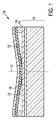
図1は、本発明によらない崩壊前の静電容量型トランスデューサーセル10の断面図を示し、図1aは図1のセルの上面図を示す。図1において、この崩壊前の静電容量型トランスデューサー10は、第1の(下部)電極16を有する基板12と、第2の(上部)電極18を有する膜14とを有する。基板12と膜14との間に空洞13が形成される。膜14は、セル10の膜14の中心C(又はセル10の中心C)にある崩壊領域において基板12に崩壊する。
FIG. 1 shows a cross-sectional view of a
図1及び図1aにおいて、空洞13における陰影又はドットは、電気機械結合を位置関数として示す。高いドットの密度は、高い結合を示す。図に示すように、膜14が基板12に崩壊して(又はピン止めされて)いるので、中心Cの周りの中心領域には結合がない。膜14が引き寄せられ、基板12と接触する地点において最も高い結合が得られる。その理由は、(固定した)下部電極16と(柔軟な)上部電極18との間にある空洞13(又は間隙)の高さが前記トランスデューサーセル10の静電容量、故にその結合を決めるからである。
1 and 1a, the shading or dots in the
図1において、膜の全領域にわたり延在している連続する上部電極18により、中心Cにおける崩壊領域は、寄生容量を追加するが、その領域は動かないので、結合は存在しない。図1に見られるように、空洞13(又は間隙)の高さは、崩壊領域の縁から外周に向かって単調増加する。中心Cから離れるほど、増分エリアは大きくなるが、空洞13(又は間隙)の高さも高くなる。高い結合領域は例えば、より多くのバイアス電圧を印加することにより増大することができる。これは、前記エリア及び崩壊領域の外周を増大させ、この外周は結合の増大をもたらす。残念なことに、これは、崩壊領域の望まない静電容量も増大させてしまう。
In FIG. 1, due to the continuous
図2は、本発明の第1の実施例による崩壊前の静電容量型トランスデューサーセル10の断面図を示し、図2aは図2のセルの上面図を示す。崩壊前の静電容量型トランスデューサーセル10は、第1の電極16を有する基板12と、第2の電極18を有する移動可能又は柔軟な膜14とを有する。第1の(下部)電極16と第2の(上部)電極18との間にコンデンサが形成される。第1の電極16は、基板の基材に付けられ、第2の電極18は膜の基材に付けられる。しかしながら、第1の電極16が前記基板の基材に組み込まれること、及び第2の電極18が前記膜の基材に組み込まれることもでき又は他の如何なる適切な方法で基材内に若しくは基材上に置かれることもできると理解されたい。
FIG. 2 shows a cross-sectional view of the
基板12と膜14との間に空洞13が形成される。例えば超音波を受信するとき、超音波が膜14を動かす又は振動させ、電極16、18の間における静電容量の変化が検出される。それにより、前記超音波は対応する電気信号に変換される。逆に、電極16、18に印加される電気信号が膜14を動かす又は振動させ、それにより超音波を送信する。
A
基板12の基材は、例えばシリコンのような導体材料又は半導体材料とすることができる。しかしながら、他の如何なる適切な材料も使用され得ると理解されたい。基板12の基材が導体又は半導体である場合、基板の基材と第1の(下部)電極16との間に絶縁層が適用される。絶縁層は第1の(下部)電極16の上に適用されることができる。このように、接触面は、共に又は全て同じ絶縁体である。膜14の基材は、例えば二酸化ケイ素、窒化ケイ素及び/又はオキシ窒化ケイ素のような絶縁材料とすることができる。しかしながら、他の如何なる適切な材料も使用され得ると理解されたい。
The base material of the
図2aに見られるように、この実施例のセル10は、中心Cを持つ円形状のセルである。このセルは、中心Cを軸に(円)対称である。このセル10は、膜14が基板12に取り付けられる外側領域22を持つ。図2の実施例において、前記セルは基板12と膜14との間に支持体15を有し、この支持体15は膜14を基板12に取り付けるのに使用される。空洞の高さ(又は間隙の厚さ)は、支持体15において(この空洞の最大の高さから)急に又は不連続的に零になる。支持体15は、円環形状の支持体とすることができる。しかしながら、膜は他の如何なる適切な方法で基板に取り付けられると理解されたい。
As can be seen in FIG. 2 a, the
セル10はさらに、外形領域22の内側にある又は外形領域22により囲まれる内側領域20を有する。この内側領域20は支持体15により制限される。セルの内側領域20に空洞が形成される。膜14は、この内側領域20内にある第1の崩壊領域24において基板12に崩壊する。この第1の崩壊領域24は、円環形状(又はリング状)である。この円環形状の第1の崩壊領域24は、セル10の中心C(又は膜14の中心C)を中心として置かれる。空洞13の高さ(又は間隙の厚さ)は、崩壊領域24において円滑に又は連続して零まで減少する。トランスデューサーセル10の最も高い結合エリアは崩壊領域24のすぐ近隣にある。従って、セルの結合は増大する。図2及び図2aにおいて、空洞13における陰影又はドットは、結合を位置関数として示す。ドットの密度の増大は、結合の増大を示している。図に示すように、セルの中心Cにおいて、結合はごく僅かであり、中心Cから崩壊領域24にかけて増大する。厳密に言えば感度は電気機械結合だけでなく、外的条件にも依存していても、電気機械結合はときどき、セルの"感度"とも呼ばれる。
The
内側領域20内に円環形状の崩壊領域24が存在しているので、第1の空洞13及び第2の空洞17が形成される。第1の空洞13は、円環形状の崩壊領域24の内側にある。言い換えると、円環形状の崩壊領域24の内側にある又はこの崩壊領域24により囲まれる領域において、膜14と基板12との間に第1の空洞13が形成される。第2の空洞17は、前記円環形状の崩壊領域24の外側にある。言い換えると、前記円環形状の崩壊領域24の外側にある又はこの崩壊領域24を囲んでいる領域において、膜14と基板12との間に第2の空洞17が形成される。この第2の空洞17は円環形状である。
Since the annular-shaped
第2の(上部)電極18は円環形状である。故に、この第2の電極18は前記円環形状の崩壊領域24に適切に適合される。このように、第2の電極18は、前記セルの静電容量の電気機械結合されない部分を最小にすることができる。電気機械結合は、変化しない静電容量の部分に膜が移動するとき、変化する静電容量の部分の比の最大化に依存する。これは、円環形状の第2の電極18を使用することにより達成され、故に崩壊領域24にわたる電極見え(electrode exposure)を最小限にする。代わりに、第2の電極18に電気接続されていない別個の電極が使用されることもできる。
The second (upper)
第2の電極18は、円環形状の第1の崩壊領域24に(少なくとも)極めて近接して(又はすぐ近隣に)置かれている。第2の電極18は、空洞13の高さが円滑に又は連続して零に減少する領域において、この第1の空洞13の上に置かれる。図2に見られるように、第2の電極18の外縁18aは、崩壊領域24が始まる地点で終了する。第2の電極18の内縁18bは、円環形状の電極18の穴を規定する。図2に示される実施例において、第2の電極18は、円環形状の第1の崩壊領域24の内側にある(又はその領域24により囲まれる)第1の変換領域26内に置かれる。言い換えると、第2の(上部)電極18は、第1の空洞13の上及び第1の(下部)電極16の上に置かれる。これがセルの活性変換区域を形成する。
The
図3は、本発明の第2の実施例による崩壊前の静電容量型トランスデューサーセルの断面図を示し、図3aは図3のセルの上面図を示す。第1の実施例に対する夫々の説明及び参照番号は、図3の実施例にも適用する。図1の第1の実施例と比較して、図3の実施例において、第2の電極18は、円環形状の第1の崩壊領域24の外側にある又はその領域24を囲んでいる第2の変換領域27内に置かれる。言い換えると、第2の電極18は、第2の空洞17の上に置かれる。第2の電極は、円環形状の第1の崩壊領域24に(少なくとも)極めて近接して(又はすぐ近隣に)置かれている。第2の電極18は、空洞17の高さが円滑に又は連続して零に減少する領域において、この空洞17の上に置かれる。図3及び図3aにおいて、空洞17における陰影又はドットは、結合を位置関数として示す。ドットの密度の増大は、結合の増大を示している。図に示すように、支持体15(又はセルの外側領域22)において結合は最少又はごく僅かであり、崩壊領域24にかけて増大している。
FIG. 3 shows a cross-sectional view of a capacitive transducer cell before collapse according to a second embodiment of the present invention, and FIG. 3a shows a top view of the cell of FIG. The respective descriptions and reference numerals for the first embodiment also apply to the embodiment of FIG. Compared to the first embodiment of FIG. 1, in the embodiment of FIG. 3, the
第1の実施例と第2の実施例とを組み合わせるのも可能であると理解されたい。このような場合、第2の電極18は、第1の変換領域26内に置かれる第1の電極部と、第2の変換領域27内に置かれる第2の電極部とを有する。
It should be understood that it is possible to combine the first embodiment with the second embodiment. In such a case, the
図4は、本発明の第3の実施例による崩壊前の静電容量型トランスデューサーセルの断面図を示し、図4aは図4のセルの上面図を示す。先行する実施例に対する夫々の説明及び参照番号は、図4の実施例にも適用する。図4の実施例のセルは、図2の実施例のセルに基づいている。しかしながら、図4の実施例において、膜14はさらに、内側領域20内に置かれる第2の崩壊領域28において基板12に崩壊している。このように、セルの電気機械結合エリアはさらに拡大する。第2の崩壊領域28は、セル10又は膜14の中心Cに置かれる。第1の空洞13はここで円環形状である。第2の崩壊領域28は、円(円環ではない)形状である。図4の実施例において、円環形状の第2の電極18は、図2を参照して説明されるように、第1の変換領域26内に置かれる。第2の電極18は、第2の崩壊領域28に(少なくとも)極めて隣接して(又はすぐ近隣に)置かれている。第2の電極は、第1の崩壊領域24にも極めて隣接して及び第2の崩壊領域28のすぐ近隣にの両方で置かれる。特に、第2の電極18の外縁18aは、第1の崩壊領域24に極めて近接して置かれ、第2の電極18の内縁18bは、第2の崩壊領域28に極めて近接して置かれる。図4及び図4aにおいて、空洞13における陰影又はドットは、結合を位置関数として示す。ドットの密度の増大は、結合の増大を示している。図に示すように、円環形状の空洞13の中央において結合は最少又はごく僅かであり、第1の崩壊領域24及び第2の崩壊領域28の両方にかけて増大している。
FIG. 4 shows a cross-sectional view of a capacitive transducer cell before collapse according to a third embodiment of the present invention, and FIG. 4a shows a top view of the cell of FIG. The respective descriptions and reference numerals for the preceding embodiments also apply to the embodiment of FIG. The cell of the embodiment of FIG. 4 is based on the cell of the embodiment of FIG. However, in the embodiment of FIG. 4, the
上述した実施例において、膜14は、恒久的に崩壊する(機械的に崩壊する)ことができる、又は膜14は、セルの動作中にのみ崩壊する(電気的に崩壊する)ことができる。ここで、図5から図8を参照して、追加の崩壊電極を使用して電気的な崩壊の事例が説明される。
In the embodiments described above, the
図5は、本発明の第4の実施例による崩壊前の静電容量型トランスデューサーセルの断面図を示す。先行する実施例に対する夫々の説明及び参照番号は、図5の実施例にも適用する。図5の実施例のセルは、図2のセルに基づいている。しかしながら、図5の実施例において、膜14はさらに、第1の崩壊領域24に置かれる第3の電極19を有する。この第3の電極19は、膜14を基板2に崩壊させるのに使用される。膜14は、第1の電極16と第3の電極19との間に(十分な)電圧を印加することにより、基板12に崩壊する。従って、膜14の第3の電極19は、膜又はセルを崩壊させるのに使用され(崩壊電極とも呼ばれる)、及び膜14の第2の電極18はセンス電極(sense electrode)である。これらの電極18、19は電気的に分離されているので、崩壊領域24は、寄生容量の一因ではない。
FIG. 5 shows a cross-sectional view of a capacitive transducer cell before collapse according to a fourth embodiment of the present invention. The respective descriptions and reference numerals for the preceding embodiment also apply to the embodiment of FIG. The cell of the embodiment of FIG. 5 is based on the cell of FIG. However, in the embodiment of FIG. 5, the
図6は、本発明の第5の実施例による崩壊前の静電容量型トランスデューサーセルの断面図を示す。先行する実施例に対する夫々の説明及び参照番号は、図6に実施例にも適用する。図6の実施例のセルは、図4の実施例のセルに基づいている。しかしながら、図6の実施例において、膜14はさらに、第1の崩壊領域24に置かれる第3の電極19(図5の説明を参照)及び第2の崩壊領域28に置かれる第4の電極21を有する。第3の電極19及び第4の電極21は、膜14を基板12に崩壊させるのに使用される。膜14は、第1の電極16と第3の電極19との間に(十分な)電圧を印加することにより、及び第1の電極16と第4の電極21との間に(十分な)電圧を印加することにより、基板12に崩壊する。従って、膜14の第3の電極19及び第4の電極21は、膜又はセルを崩壊させるのに使用され(崩壊電極とも呼ばれる)、膜14の第2の電極18はセンス電極である。
FIG. 6 shows a cross-sectional view of a capacitive transducer cell before collapse according to a fifth embodiment of the present invention. The respective descriptions and reference numerals for the preceding embodiment also apply to the embodiment in FIG. The cell of the embodiment of FIG. 6 is based on the cell of the embodiment of FIG. However, in the embodiment of FIG. 6, the
図7は、本発明の第6の実施例による崩壊前の静電容量型トランスデューサーセル10の断面図を示す。先行する実施例に対する夫々の説明及び参照番号は、図7の実施例にも適用する。図7の実施例のセルは、第1の実施例と第2の実施例とを組み合わせたセルに基づいている。従って、第2の電極は、(第1の変換領域26内に置かれる)第1の円環形状の電極部18'及び(第2の変換領域27内に置かれる)第2の円環形状の電極部18"を有する。しかしながら、図7の実施例において、膜14はさらに、第1の崩壊領域24に置かれる第3の電極19を有する(図5又は図6の説明を参照)。第3の電極は従って(円環形状の崩壊領域24の内側にある)第1の円環形状の(内側)電極部18'と、(円環形状の崩壊領域24の外側にある)第2の円環形状の(外側)電極部18"との間に置かれる。
FIG. 7 shows a cross-sectional view of a
図8a−8cは各々、図6の第5の実施例による崩壊前の静電容量型トランスデューサーセルの電極の上面図の異なる例を示す。図8a−8cの各々において、第2の(センス)電極18、第3の(崩壊)電極19及び第4の(崩壊)電極21が示される。第2の(センス)電極18は、第3の(崩壊)電極19及び/又は第4の(崩壊)電極21とは電気的に分離されている。第3及び第4の(崩壊)電極19、21は電気接続されている。しかしながら、第3及び第4の(崩壊)電極19、21に別々の電圧を印加する必要がある又は印加を望む場合、第3及び第4の(崩壊)電極19、21が電気的に分離されることもできる。
8a-8c each show different examples of top views of the electrodes of the capacitive transducer cell before collapse according to the fifth embodiment of FIG. In each of FIGS. 8a-8c, a second (sense)
図8b又は8cは、第2の円環形状の電極18とのコネクタ38、並びに第3の電極19及び第4の電極21とのコネクタ39も示す。従って、図8b又は8cは、中心への独立したアクセスを与えるための電極を通すために例示的な電極形状を示す。図8a−8cの各々において、中心への独立したアクセスは、電極21を電極18に接続することなく、この電極21への電圧を得るのに必要である。図8aにおいて、これは例えば電極18の上部にわたるバイアスにより達成される。しかしながら、これは幾つかの余分なステップ、追加のコスト及び装置の複雑さを要求する。図8bにおいて、第2の電極18は、この電極の円環形状において1つの開口を持ち、第3の電極19は、この電極の円環形状において1つの開口を持つ。第4の電極21へのコネクタ39は、第2の電極18の開口内に置かれ、第2の電極18へのコネクタ38は、第3の電極19の開口内に置かれる。図8cにおいて、第2の電極18は、この電極の円環形状において複数の開口を持ち、第3の電極19は、この電極の円環形状において複数の開口を持つ。このように、第2の電極18及び第3の電極19は各々セグメントに分けられている。図8cにおいて、電極18、19の各々は、4つのセグメントに分けられている。さらに近似した放射相称を与えるために、各電極をさらに多くのセグメントに分けることが望ましい。しかしながら、これら電極がより少ないセグメント、従って少なくとも2つのセグメントに分けられることもできる。これらセグメントは、前記内側領域(又は膜領域)の外側において外部から接続されることができる。図8cに見られるように、第2の電極18との各々のコネクタ38は、第3の電極19の2つのセグメントの間を延在している。各々のコネクタ39は、第2の電極18の2つのセグメントの間を延在している。言い換えると、第4の電極21への1つのコネクタ39は、第2の電極18の各々の開口内に置かれ、第2の電極18への1つのコネクタ38は、第3の電極19の各々の開口内に置かれる。
FIG. 8 b or 8 c also shows a
一般的に、崩壊前のセルにおいて、例えば電気的な崩壊又は機械的な崩壊を用いるような、異なる方法を用いて膜が崩壊することができる。ある例において、膜14は、内側領域に内部応力を持つことができる。特に、この内部応力が膜14を基板から離れて膨らませることができる。このように、膜14と基板12との間に空洞13、17が設けられる。内部応力が無いと、第1の変換領域26(円環形状の崩壊領域24の内側にある又はこの領域24により囲まれる領域)は、基板12と接したまま留まる。
In general, in a cell prior to collapse, the membrane can collapse using different methods, such as using electrical or mechanical collapse. In one example, the
ある例において、第1の変換領域25における膜14の残留応力は、空洞13(又は間隙)が存在するように圧縮されることができる。この圧縮される応力の領域は、膜の中立面と、空洞若しくは間隙から遠位にある(又は離れた側を向く)膜の表面との間になければならない。さらに、圧縮される応力の領域は、円環形状の崩壊領域の中心から略半径に延在することができる。プレート及びシェルの機械工学の理論において知られるように、膜が曲げられるとき、伸長又は圧縮を受けない中立面が膜に存在する。この中立面の一方の側にある如何なる圧縮応力も、応力を受けた側から離れて凹むように膜を曲げ、反対に中立面の一方の側の如何なる引張応力も応力を受けた側に向かい凹むように膜を曲げる。
In one example, the residual stress of the
代替例において、前記応力は、張力であり及び膜の中立面と、空洞若しくは間隙に隣接する(又はそれに向いている)膜の表面との間にある。他の例は、崩壊したリングの遠位及びその上にある張力、崩壊したリングの近位及びその上にある圧縮、又は上述した例の如何なる組み合わせを含むこともできる。さらに、例えば圧縮及び遠位又は張力及び近位のような崩壊したリングの外側に追加の層が存在することができる。 In an alternative, the stress is tension and is between the neutral surface of the membrane and the surface of the membrane adjacent to (or facing) the cavity or gap. Other examples may include the tension distal and over the collapsed ring, the compression proximal and over the collapsed ring, or any combination of the above examples. In addition, there can be additional layers on the outside of the collapsed ring, such as compression and distal or tension and proximal.
膜の内部応力は例えば、膜の化学量論により又は異なる材料による多層の膜と、これら膜にある応力とを使用することにより制御されることができる。例えば、材料析出条件も膜の応力に影響を及ぼす。特別な例として、膜の基材が二酸化ケイ素、窒化ケイ素及び/又はオキシ酸化ケイ素から作られる場合、二酸化ケイ素は圧縮であり、窒化ケイ素は張力である、及びオキシ酸化ケイ素における応力は、化学量論を用いて制御されることができる。電極材料の構成は、前記応力にも影響を及ぼすことがある。電極材料及び堆積パラメタの選択を介した、並びに適切な追加の材料からなるパターン層を介した、追加の応力の寄与は含まれる。 The internal stress of the membrane can be controlled, for example, by the stoichiometry of the membrane or by using multiple layers of different materials and the stresses in these membranes. For example, material deposition conditions also affect film stress. As a special example, if the membrane substrate is made from silicon dioxide, silicon nitride and / or silicon oxyoxide, the silicon dioxide is compressive, the silicon nitride is tension, and the stress in the silicon oxyoxide is the stoichiometry. Can be controlled using theory. The configuration of the electrode material may affect the stress. Additional stress contributions are included through the selection of electrode materials and deposition parameters, and through pattern layers of appropriate additional materials.
図9は、本発明の他の実施例による崩壊前の静電容量型トランスデューサーセルの断面図を示し、図9aは、図9のセルの上面図を示す。先行する実施例に対する夫々の説明及び参照番号は、図9の実施例にも適用する。図9の実施例において、膜14は、基板12(又は電極16)の平面上にある柱又は突起部15aにより、中央領域29において基板12に取り付けられている。突起部15aは、基板12と膜14との間に置かれる。第1の円環形状の空洞13は、突起部15aを取り囲む領域において膜14と基板12との間に形成される。好ましくは突起部15aは、支持体15を設けるのと同じ処理ステップで設けられる。突起部15aは円形状であり、セルの中心Cの周りの中央領域29に置かれる。空洞13の高さ(又は間隙の厚さ)は、突起部15aにおいて(空洞の最大の高さから)急に又は不連続に零になる。従って、突起部15aは、第2の崩壊領域ではなく、故に(第2の崩壊領域を持つ図4又は図6の実施例に比べ)多くの結合は提供しない。しかしながら、図9の実施例は、強固であり、製造が容易である。図9の実施例において、膜14は、第3の(崩壊)電極19に印加されるバイアス電圧により崩壊し、膜14に応力を加えることで崩壊はしない。従って、図9の実施例において、膜の内部応力は必要ない。
9 shows a cross-sectional view of a capacitive transducer cell before collapse according to another embodiment of the present invention, and FIG. 9a shows a top view of the cell of FIG. The respective descriptions and reference numerals for the preceding embodiments also apply to the embodiment of FIG. In the embodiment of FIG. 9, the
図9及び図9aにおいて、第1の空洞13及び第2の空洞17における陰影又はドットは、結合を位置関数として示す。ドットの密度の増大は、結合の増大を示している。図に示すように、円環形状の第2の空洞17において、支持体15(又はセルの外側領域22)における結合は最少又はごく僅かであり、崩壊領域24にかけて増大する。円環形状の第1の空洞13において、突起部15a(又は中心C)における結合は最少又はごく僅かであり、崩壊領域24にかけて増大する。
9 and 9a, the shading or dots in the
図9の断面図は、図9aの上面図に見られるように、1つの単独(円形状)セル10を示していると指摘される。セル10は、中心C又は中心の突起部15aの周りで(円)対称である。さらに、図9の実施例において、第2の電極は、(第1の変換領域26内にある)第1の円環形状の電極部18'及び(第2の変換領域27内にある)第2の円環形状の電極部18"を有する。しかしながら、第2の電極は、第1の変換領域26又は第2の変換領域27の何れか一方にだけ置かれることもできると理解されたい。
It is noted that the cross-sectional view of FIG. 9 shows one single (circular)
図2から図9を参照して上述した実施例において、第1の(下部)電極16は、基板の基材に付けられる、及び内側領域20(又は膜若しくはセル)全体にわたり延在している連続層であるように示されている。しかしながら、他の如何なる適切な第1の電極が用いられ得ると理解されたい。例えば第1の電極は、円環形状の電極とすることができる及び/又は内側領域(又は膜若しくはセル)全体にわたり延在しないこともできる。図2から図7を参照して上述した実施例において、第2の電極18は、円環形状の電極である、及び内側領域20(又は膜若しくはセル)全体にわたり延在していなくても、他の如何なる適切な第2の電極が用いられ得ると理解されたい。例えば、第2の電極は、円環形状の電極とすることができる及び/又は内側領域(又は膜若しくはセル)全体にわたり延在することができる。ここに開示される全ての事例又は実施例において、電極の形状は、トランスデューサーセルの動作に影響を及ぼすことなく、膜と基板との間で交換されてもよい。
In the embodiment described above with reference to FIGS. 2-9, the first (lower)
図2から図9を参照して上述した実施例において、セル10は円形状のセルである。円形状は、利用可能な空間のかなり良い充填及び/又はほんのわずか高い次元の振動モード、特に送信されるエネルギーに望ましいモードと競合する又は所望する受信信号を不明瞭にする不要な信号を作る振動モードを提供する。しかしながら、他の如何なるセルの形状、例えば楕円形、多角形、六角形、矩形又は正方形等も使用され得ると理解されたい。従って、概念を説明するのに使用される円対称が限定であると考えるべきではない。
In the embodiment described above with reference to FIGS. 2 to 9, the
本発明はさらに、以下の実施例の1つ以上に基づいて説明されることができる。第1の実施例において、中心における通常の崩壊領域に代わり又はそれに加えて、この中心から離れた円環領域において崩壊を引き起こす。このように、活性変換のエリアが大きく増大する。第2の実施例において、1又は2つの電極が崩壊領域に設けてもよく、1つ目は装置の中心に、2つ目は外周の周りに設けられる。第3の実施例において、変換のために別個の円環電極が与えられる。第4の実施例において、膜は、変換領域においてこの膜を基板から離れるように膨らませる内部応力分布を用いて構成される。 The invention can be further described based on one or more of the following examples. In the first embodiment, instead of or in addition to the normal collapse region at the center, it causes collapse in the toric region away from this center. Thus, the area of activity conversion is greatly increased. In the second embodiment, one or two electrodes may be provided in the collapse region, the first being provided at the center of the device and the second being provided around the periphery. In a third embodiment, a separate annular electrode is provided for conversion. In a fourth embodiment, the membrane is constructed using an internal stress distribution that causes the membrane to swell away from the substrate in the conversion region.
技術的観点から、本発明の崩壊前の静電容量型トランスデューサーセル(特にcMUT)は原則的に、例えば国際出願公開番号第2010/032156に詳細に開示される従来の"無崩壊の"静電容量型トランスデューサーセル(特にcMUT)と同じ又は同様の方法で製造されることができ、この公報は、参照により含まれるものとする。 From a technical point of view, the pre-collapse capacitive transducer cell (especially cMUT) of the present invention is in principle the conventional “non-collapse” static disclosed in detail, for example, in International Application Publication No. 2010/032156. It can be manufactured in the same or similar manner as a capacitive transducer cell (especially cMUT) and this publication is incorporated by reference.
本発明は、超音波を送信及び/又は受信する如何なる静電容量型トランスデューサーセル(cMUT)、特に(例えば少なくとも30MHzまで又はそれよりも高い)多重電極構造を支持するのに十分な大きさのcMUTセルに応用可能である。しかしながら、原則的に本発明は、例えば圧力を測定するための圧力センサー又はトランスデューサーのような他の如何なる崩壊前の静電容量型トランスデューサーにも応用可能である。トランスデューサーという言葉はセンサーの特別な事例も含んでいると理解されたい。 The present invention is sufficiently large to support any capacitive transducer cell (cMUT) that transmits and / or receives ultrasound, particularly a multi-electrode structure (eg, up to at least 30 MHz or higher). Applicable to cMUT cells. In principle, however, the invention is applicable to any other pre-collapse capacitive transducer, such as a pressure sensor or transducer for measuring pressure, for example. It should be understood that the term transducer includes special cases of sensors.
本発明が図面及び上記説明において詳細に説明及び記載されているのに対し、このような説明及び記載は、説明的又は例示的であり、限定的であるとは考えるべきではない。本発明は開示される実施例に限定はされない。開示した実施例以外の変形例は、図面、明細書及び特許請求の範囲を学ぶことにより、請求する本発明を実施する当業者により理解及びもたらされることができる。 While the invention has been illustrated and described in detail in the drawings and foregoing description, such description and description are to be considered illustrative or exemplary and not restrictive. The invention is not limited to the disclosed embodiments. Variations other than the disclosed embodiments can be understood and effected by those skilled in the art of practicing the claimed invention, upon studying the drawings, specification and claims.
請求項において、"有する"という言葉は、他の要素又はステップを排除するものではなく、複数あると述べないことが、それらが複数あることを排除するものではない。単独の要素又は他のユニットが請求項に挙げられる幾つかのアイテムの機能を果たしてもよい。ある方法が互いに異なる従属請求項に挙げられているという単なる事実は、これらの方法の組み合わせが有利に用いられないことを示してはいない。 In the claims, the word “comprising” does not exclude other elements or steps, and the absence of a plurality does not exclude the presence of a plurality. A single element or other unit may fulfill the functions of several items recited in the claims. The mere fact that certain methods are recited in mutually different dependent claims does not indicate that a combination of these methods cannot be used to advantage.
これら請求項における如何なる参照符号は、その範囲を限定するとは考えない。 Any reference signs in the claims should not be construed as limiting the scope.
Claims (15)
−第2の電極を有する膜、
−前記膜が前記基板に取り付けられている、支持体を含む外側領域、及び
−前記外側領域により囲まれる内側領域
を有する崩壊前の静電容量型トランスデューサーセルにおいて、
前記膜は、前記内側領域内に置かれる円環形状の第1の崩壊領域において前記基板に崩壊して、前記円環形状の第1の崩壊領域を囲む、前記膜と前記基板との間の円環形状の空洞を形成し、前記円環形状の空洞の高さは前記支持体から前記円環形状の第1の崩壊領域まで連続して減少し、
前記第2の電極は、前記円環形状の第1の崩壊領域を囲んでいる変換領域を設けるように前記円環形状の空洞の上に置かれる、
セル。 A substrate having a first electrode;
A membrane having a second electrode;
- the membrane is attached to the substrate, an outer region comprising a support, and - in capacitive transducer cells before disruption having an inner region surrounded by said outer region,
The membrane collapses into the substrate in an annular first collapse region located in the inner region and surrounds the annular first collapse region between the membrane and the substrate Forming an annular cavity, the height of the annular cavity continuously decreasing from the support to the first collapsed area of the annular shape;
The second electrode is placed on the cavity of the annular shape so as to provide a conversion region surrounding the first collapse region of the annular shape,
cell.
−第2の電極を有する膜、
−前記膜が前記基板に取り付けられている外側領域、及び
−前記外側領域の内側にある又は前記外側領域により囲まれる内側領域
を有する崩壊前の静電容量型トランスデューサーセルにおいて、
前記膜は、前記内側領域内に置かれる円環形状の第1の崩壊領域において前記基板に崩壊し、
前記セルは、前記円環形状の第1の崩壊領域の内側にある又は前記崩壊領域により囲まれる第1の変換領域と、前記円環形状の第1の崩壊領域の外側にある又は前記崩壊領域を囲んでいる第2の変換領域とを有し、
前記内側領域内に置かれる第2の崩壊領域及び前記第2の崩壊領域内に置かれる第4の電極を更に有する、セル。 A substrate having a first electrode;
A membrane having a second electrode;
An outer region where the membrane is attached to the substrate; and
-An inner region that is inside or surrounded by the outer region;
In the capacitive transducer cell before collapse having
The membrane collapses into the substrate in a toroidal first collapse region located in the inner region;
The cell is a first transformation region that is inside or surrounded by the ring-shaped first collapse region, and is outside the ring-shaped first collapse region or the collapse region A second transformation region surrounding
The cell further comprising a second collapse region placed in the inner region and a fourth electrode placed in the second collapse region.
−第2の電極を有する膜、
−前記膜が前記基板に取り付けられている外側領域、及び
−前記外側領域の内側にある又は前記外側領域により囲まれる内側領域
を有する崩壊前の静電容量型トランスデューサーセルにおいて、
前記膜は、前記内側領域内に置かれる円環形状の第1の崩壊領域において前記基板に崩壊し、
前記セルは、前記円環形状の第1の崩壊領域の内側にある又は前記崩壊領域により囲まれる第1の変換領域と、前記円環形状の第1の崩壊領域の外側にある又は前記崩壊領域を囲んでいる第2の変換領域とを有し、
前記膜はさらに、前記内側領域内に置かれる第2の崩壊領域において前記基板に崩壊する、セル。 A substrate having a first electrode;
A membrane having a second electrode;
An outer region where the membrane is attached to the substrate; and
-An inner region that is inside or surrounded by the outer region;
In the capacitive transducer cell before collapse having
The membrane collapses into the substrate in a toroidal first collapse region located in the inner region;
The cell is a first transformation region that is inside or surrounded by the ring-shaped first collapse region, and is outside the ring-shaped first collapse region or the collapse region A second transformation region surrounding
The film is further disintegrate the substrate in the second collapse region is placed in the inner region, the cell.
−第1の電極を有する基板を設けるステップと、
−第2の電極を有する膜を設けるステップであり、前記セルは、前記膜が前記基板に取り付けられている、支持体を含む外側領域と、前記外側領域により囲まれる内側領域とを持つ、前記膜を設けるステップと、
−前記内側領域内に置かれる円環形状の第1の崩壊領域において、前記膜を前記基板に崩壊させて、前記膜と前記基板との間に円環形状の空洞を形成するステップであって、前記円環形状の空洞は前記円環形状の第1の崩壊領域を囲み、前記円環形状の空洞の高さは前記支持体から前記円環形状の第1の崩壊領域まで連続して減少する、ステップと、
−前記円環形状の第1の崩壊領域を囲んでいる変換領域を設けるステップと
を有し、前記第2の電極を有する膜を設けるステップは、前記第2の電極を前記円環形状の空洞の上に置くステップを含む、方法。 In a method of manufacturing a capacitive transducer cell before collapse,
- a step of providing a substrate having a first electrode,
- a step of providing a film having a second electrode, the cell, the membrane is attached to said substrate, having an outer region comprising a support and an inner region surrounded by said outer region, the comprising the steps of: providing a membrane,
- in the first collapsed region of annular shape is placed in the inner region, the membrane disintegrate in the substrate, met steps that form a cavity of annular shape between the film and the substrate The annular cavity surrounds the first annular collapse region, and the height of the annular cavity continues from the support to the annular first collapse region. Decreasing, steps ,
- said first collapsed region have a enclosing the step of providing a transform domain are <br/> of annular shape, said step of providing a membrane having a second electrode, the circular said second electrode Placing the method over an annular cavity .
−第1の電極を有する基板を設けるステップ、
−第2の電極を有する膜を設けるステップであり、前記セルは、前記膜が前記基板に取り付けられている外側領域と、前記外側領域の内側にある又は前記外側領域により囲まれる内側領域とを持つ、前記膜を設けるステップ、並びに
−前記内側領域内に置かれる円環形状の第1の崩壊領域において、前記膜を前記基板に崩壊させるステップ、及び
−前記円環形状の第1の崩壊領域の内側にある又は前記崩壊領域により囲まれる第1の変換領域と、前記円環形状の第1の崩壊領域の外側にある又は前記崩壊領域を囲んでいる第2の変換領域とを設けるステップ
を有し、
前記膜はさらに、前記第1の崩壊領域に置かれる第3の電極を有し、
前記膜を前記基板に崩壊させるステップは、前記第1の電極と前記第3の電極との間に電圧を印加するステップを有する、方法。 In a method of manufacturing a capacitive transducer cell before collapse,
Providing a substrate having a first electrode;
Providing a membrane having a second electrode, the cell comprising an outer region where the membrane is attached to the substrate and an inner region that is inside or surrounded by the outer region; Having the step of providing the membrane; and
-Collapsing the membrane into the substrate in an annular shaped first collapse region located in the inner region; and
A first transformation region that is inside or surrounded by the collapsed first collapse region, and that is outside or surrounding the collapsed first collapse region Providing a second conversion region
Have
The membrane further have a third electrode to be placed in the first collapsed region,
The method of collapsing the film into the substrate comprises applying a voltage between the first electrode and the third electrode.
Applications Claiming Priority (3)
| Application Number | Priority Date | Filing Date | Title |
|---|---|---|---|
| US201161560836P | 2011-11-17 | 2011-11-17 | |
| US61/560,836 | 2011-11-17 | ||
| PCT/IB2012/056152 WO2013072803A1 (en) | 2011-11-17 | 2012-11-05 | Pre-collapsed capacitive micro-machined transducer cell with annular-shaped collapsed region |
Publications (3)
| Publication Number | Publication Date |
|---|---|
| JP2014533907A JP2014533907A (en) | 2014-12-15 |
| JP2014533907A5 JP2014533907A5 (en) | 2015-12-17 |
| JP6265906B2 true JP6265906B2 (en) | 2018-01-24 |
Family
ID=47324242
Family Applications (1)
| Application Number | Title | Priority Date | Filing Date |
|---|---|---|---|
| JP2014541778A Active JP6265906B2 (en) | 2011-11-17 | 2012-11-05 | Capacitance-type transducer cell before collapse with a ring-shaped collapse region |
Country Status (9)
| Country | Link |
|---|---|
| US (2) | US9762148B2 (en) |
| EP (1) | EP2747905B1 (en) |
| JP (1) | JP6265906B2 (en) |
| CN (1) | CN103958079B (en) |
| BR (1) | BR112014011644A2 (en) |
| IN (1) | IN2014CN03656A (en) |
| MX (1) | MX2014005795A (en) |
| RU (1) | RU2609917C2 (en) |
| WO (1) | WO2013072803A1 (en) |
Families Citing this family (44)
| Publication number | Priority date | Publication date | Assignee | Title |
|---|---|---|---|---|
| JP6210992B2 (en) * | 2011-10-28 | 2017-10-11 | コーニンクレッカ フィリップス エヌ ヴェKoninklijke Philips N.V. | Pre-crushing capacity micromachined transducer cell with stress layer |
| US20160199030A1 (en) * | 2013-08-27 | 2016-07-14 | Koninklijke Philips N.V. | Dual mode cmut transducer |
| JP6474139B2 (en) * | 2013-08-30 | 2019-02-27 | コーニンクレッカ フィリップス エヌ ヴェKoninklijke Philips N.V. | Capacitive micromachined ultrasonic transducer cell |
| EP3052250B1 (en) * | 2013-09-27 | 2022-03-30 | Koninklijke Philips N.V. | Ultrasound transducer assembly and method for transmitting and receiving ultrasound waves |
| US11241715B2 (en) | 2015-06-30 | 2022-02-08 | Koninklijke Philips N.V. | Ultrasound system and ultrasonic pulse transmission method |
| US10445547B2 (en) | 2016-05-04 | 2019-10-15 | Invensense, Inc. | Device mountable packaging of ultrasonic transducers |
| US10670716B2 (en) | 2016-05-04 | 2020-06-02 | Invensense, Inc. | Operating a two-dimensional array of ultrasonic transducers |
| US10315222B2 (en) | 2016-05-04 | 2019-06-11 | Invensense, Inc. | Two-dimensional array of CMOS control elements |
| US10656255B2 (en) * | 2016-05-04 | 2020-05-19 | Invensense, Inc. | Piezoelectric micromachined ultrasonic transducer (PMUT) |
| US10452887B2 (en) | 2016-05-10 | 2019-10-22 | Invensense, Inc. | Operating a fingerprint sensor comprised of ultrasonic transducers |
| US10706835B2 (en) | 2016-05-10 | 2020-07-07 | Invensense, Inc. | Transmit beamforming of a two-dimensional array of ultrasonic transducers |
| US10441975B2 (en) | 2016-05-10 | 2019-10-15 | Invensense, Inc. | Supplemental sensor modes and systems for ultrasonic transducers |
| US10600403B2 (en) | 2016-05-10 | 2020-03-24 | Invensense, Inc. | Transmit operation of an ultrasonic sensor |
| US10562070B2 (en) | 2016-05-10 | 2020-02-18 | Invensense, Inc. | Receive operation of an ultrasonic sensor |
| US11673165B2 (en) | 2016-05-10 | 2023-06-13 | Invensense, Inc. | Ultrasonic transducer operable in a surface acoustic wave (SAW) mode |
| US10539539B2 (en) | 2016-05-10 | 2020-01-21 | Invensense, Inc. | Operation of an ultrasonic sensor |
| US10408797B2 (en) | 2016-05-10 | 2019-09-10 | Invensense, Inc. | Sensing device with a temperature sensor |
| US10632500B2 (en) | 2016-05-10 | 2020-04-28 | Invensense, Inc. | Ultrasonic transducer with a non-uniform membrane |
| WO2018041658A2 (en) * | 2016-08-30 | 2018-03-08 | Koninklijke Philips N.V. | Imaging device with ultrasound transducer array |
| US10891461B2 (en) | 2017-05-22 | 2021-01-12 | Invensense, Inc. | Live fingerprint detection utilizing an integrated ultrasound and infrared sensor |
| US10474862B2 (en) | 2017-06-01 | 2019-11-12 | Invensense, Inc. | Image generation in an electronic device using ultrasonic transducers |
| US10643052B2 (en) | 2017-06-28 | 2020-05-05 | Invensense, Inc. | Image generation in an electronic device using ultrasonic transducers |
| US10984209B2 (en) | 2017-12-01 | 2021-04-20 | Invensense, Inc. | Darkfield modeling |
| WO2019109010A1 (en) | 2017-12-01 | 2019-06-06 | Invensense, Inc. | Darkfield tracking |
| US10997388B2 (en) | 2017-12-01 | 2021-05-04 | Invensense, Inc. | Darkfield contamination detection |
| US11151355B2 (en) | 2018-01-24 | 2021-10-19 | Invensense, Inc. | Generation of an estimated fingerprint |
| EP3533386A1 (en) | 2018-02-28 | 2019-09-04 | Koninklijke Philips N.V. | Pressure sensing with capacitive pressure sensor |
| US10755067B2 (en) | 2018-03-22 | 2020-08-25 | Invensense, Inc. | Operating a fingerprint sensor comprised of ultrasonic transducers |
| CN108793061B (en) * | 2018-05-25 | 2020-11-27 | 岭南师范学院 | Preparation method of full-electrode convex-pattern structure CMUT device |
| CN112533529A (en) * | 2018-08-09 | 2021-03-19 | 皇家飞利浦有限公司 | Endoluminal device with capacitive pressure sensor |
| CN109530194B (en) * | 2018-10-18 | 2020-07-14 | 天津大学 | Multi-electrode CMUT unit and multi-frequency type capacitive micro-mechanical ultrasonic transducer |
| US10936843B2 (en) | 2018-12-28 | 2021-03-02 | Invensense, Inc. | Segmented image acquisition |
| KR102196437B1 (en) * | 2019-01-29 | 2020-12-30 | 한국과학기술연구원 | Capacitive Micromachined Ultrasonic Transducer |
| CN109909140B (en) * | 2019-03-06 | 2021-06-04 | 中国工程物理研究院电子工程研究所 | Piezoelectric micromechanical ultrasonic transducer and preparation method thereof |
| US11188735B2 (en) | 2019-06-24 | 2021-11-30 | Invensense, Inc. | Fake finger detection using ridge features |
| WO2020264046A1 (en) | 2019-06-25 | 2020-12-30 | Invensense, Inc. | Fake finger detection based on transient features |
| US11216632B2 (en) | 2019-07-17 | 2022-01-04 | Invensense, Inc. | Ultrasonic fingerprint sensor with a contact layer of non-uniform thickness |
| US11176345B2 (en) | 2019-07-17 | 2021-11-16 | Invensense, Inc. | Ultrasonic fingerprint sensor with a contact layer of non-uniform thickness |
| US11232549B2 (en) | 2019-08-23 | 2022-01-25 | Invensense, Inc. | Adapting a quality threshold for a fingerprint image |
| US11392789B2 (en) | 2019-10-21 | 2022-07-19 | Invensense, Inc. | Fingerprint authentication using a synthetic enrollment image |
| CN115551650A (en) | 2020-03-09 | 2022-12-30 | 应美盛公司 | Ultrasonic fingerprint sensor with contact layer of non-uniform thickness |
| US11243300B2 (en) | 2020-03-10 | 2022-02-08 | Invensense, Inc. | Operating a fingerprint sensor comprised of ultrasonic transducers and a presence sensor |
| US11328165B2 (en) | 2020-04-24 | 2022-05-10 | Invensense, Inc. | Pressure-based activation of fingerprint spoof detection |
| TWI814403B (en) * | 2022-05-26 | 2023-09-01 | 佳世達科技股份有限公司 | Ultrasonic transducer |
Family Cites Families (16)
| Publication number | Priority date | Publication date | Assignee | Title |
|---|---|---|---|---|
| JP4378617B2 (en) | 2001-07-17 | 2009-12-09 | Smc株式会社 | Micro electromechanical sensor |
| US8008835B2 (en) * | 2004-02-27 | 2011-08-30 | Georgia Tech Research Corporation | Multiple element electrode cMUT devices and fabrication methods |
| US20060004289A1 (en) * | 2004-06-30 | 2006-01-05 | Wei-Cheng Tian | High sensitivity capacitive micromachined ultrasound transducer |
| JP4724505B2 (en) * | 2005-09-09 | 2011-07-13 | 株式会社日立製作所 | Ultrasonic probe and manufacturing method thereof |
| US7615834B2 (en) * | 2006-02-28 | 2009-11-10 | The Board Of Trustees Of The Leland Stanford Junior University | Capacitive micromachined ultrasonic transducer(CMUT) with varying thickness membrane |
| CN101772383B (en) * | 2007-07-31 | 2011-11-02 | 皇家飞利浦电子股份有限公司 | CMUTs with a high-K dielectric |
| US10092270B2 (en) * | 2007-09-17 | 2018-10-09 | Koninklijke Philips Electronics N.V. | Pre-collapsed CMUT with mechanical collapse retention |
| WO2009037655A2 (en) * | 2007-09-17 | 2009-03-26 | Koninklijke Philips Electronics, N.V. | Production of pre-collapsed capacitive micro-machined ultrasonic transducers and applications thereof |
| WO2009041675A1 (en) * | 2007-09-25 | 2009-04-02 | Canon Kabushiki Kaisha | Electrostatic transducer and manufacturing method therefor |
| JP5408935B2 (en) | 2007-09-25 | 2014-02-05 | キヤノン株式会社 | Electromechanical transducer and manufacturing method thereof |
| US8559274B2 (en) | 2007-12-03 | 2013-10-15 | Kolo Technologies, Inc. | Dual-mode operation micromachined ultrasonic transducer |
| CN101896288B (en) * | 2007-12-14 | 2013-03-27 | 皇家飞利浦电子股份有限公司 | Collapsed mode operable CMUT including contoured substrate |
| EP2145696A1 (en) * | 2008-07-15 | 2010-01-20 | UAB Minatech | Capacitive micromachined ultrasonic transducer and its fabrication method |
| CN102159334A (en) | 2008-09-16 | 2011-08-17 | 皇家飞利浦电子股份有限公司 | Capacitive micromachined ultrasound transducer |
| EP2269746B1 (en) | 2009-07-02 | 2014-05-14 | Nxp B.V. | Collapsed mode capacitive sensor |
| JP2012095112A (en) * | 2010-10-27 | 2012-05-17 | Olympus Corp | Ultrasonic generation unit |
-
2012
- 2012-11-05 IN IN3656CHN2014 patent/IN2014CN03656A/en unknown
- 2012-11-05 RU RU2014124363A patent/RU2609917C2/en not_active IP Right Cessation
- 2012-11-05 US US14/351,888 patent/US9762148B2/en active Active
- 2012-11-05 EP EP12798402.9A patent/EP2747905B1/en active Active
- 2012-11-05 CN CN201280056554.2A patent/CN103958079B/en active Active
- 2012-11-05 MX MX2014005795A patent/MX2014005795A/en unknown
- 2012-11-05 JP JP2014541778A patent/JP6265906B2/en active Active
- 2012-11-05 BR BR112014011644A patent/BR112014011644A2/en not_active Application Discontinuation
- 2012-11-05 WO PCT/IB2012/056152 patent/WO2013072803A1/en active Application Filing
-
2017
- 2017-08-22 US US15/683,097 patent/US10128777B2/en active Active
Also Published As
| Publication number | Publication date |
|---|---|
| CN103958079B (en) | 2016-08-24 |
| BR112014011644A2 (en) | 2017-05-02 |
| US20140265721A1 (en) | 2014-09-18 |
| US20170353129A1 (en) | 2017-12-07 |
| EP2747905A1 (en) | 2014-07-02 |
| IN2014CN03656A (en) | 2015-10-16 |
| JP2014533907A (en) | 2014-12-15 |
| RU2014124363A (en) | 2015-12-27 |
| EP2747905B1 (en) | 2021-10-20 |
| RU2609917C2 (en) | 2017-02-07 |
| US9762148B2 (en) | 2017-09-12 |
| US10128777B2 (en) | 2018-11-13 |
| CN103958079A (en) | 2014-07-30 |
| WO2013072803A1 (en) | 2013-05-23 |
| MX2014005795A (en) | 2014-05-30 |
Similar Documents
| Publication | Publication Date | Title |
|---|---|---|
| JP6265906B2 (en) | Capacitance-type transducer cell before collapse with a ring-shaped collapse region | |
| US10576500B2 (en) | Piezoelectric micro-machined ultrasonic transducer (PMUT) and method for manufacturing the PMUT | |
| JP5559818B2 (en) | Pre-crush CMUT with mechanical crush holding function | |
| US7612635B2 (en) | MEMS acoustic filter and fabrication of the same | |
| KR102042869B1 (en) | Ultra Wide Bandwidth Transducer With Dual Electrode | |
| JP6190450B2 (en) | Multi-frequency ultra wide bandwidth converter | |
| US8004373B2 (en) | MEMS ultrasonic device having a PZT and cMUT | |
| US8559274B2 (en) | Dual-mode operation micromachined ultrasonic transducer | |
| US8451693B2 (en) | Micromachined ultrasonic transducer having compliant post structure | |
| US20090152980A1 (en) | Electrostatic Comb Driver Actuator/Transducer and Fabrication of the Same | |
| JP2009182838A (en) | Elastic wave transducer, elastic wave transducer array, ultrasonic probe, and ultrasonic imaging apparatus | |
| JP6210992B2 (en) | Pre-crushing capacity micromachined transducer cell with stress layer | |
| JP5961697B2 (en) | Pre-collapsed capacitive micromachined transducer cell with plug | |
| KR101593994B1 (en) | High power ultrasonic transducer | |
| KR101761819B1 (en) | Ultrasonic transducer and method of manufacturing the sames | |
| JP2019114958A (en) | Electro-acoustic transducer | |
| JP6752727B2 (en) | Ultrasound Transducer and Ultrasound Imaging Device | |
| CN110434044B (en) | Electrode shape-regulated high-ultrasonic wave transceiving performance CMUTs | |
| AU2421000A (en) | Pressure tolerant transducer | |
| KR101893486B1 (en) | Rigid Backplate Structure Microphone and Method of Manufacturing the Same | |
| CN115025959A (en) | Center-supported piezoelectric type micro-mechanical ultrasonic transducer | |
| CN115193673A (en) | Micromechanical ultrasonic transducer with free side boundary |
Legal Events
| Date | Code | Title | Description |
|---|---|---|---|
| A521 | Request for written amendment filed |
Free format text: JAPANESE INTERMEDIATE CODE: A523 Effective date: 20151029 |
|
| A621 | Written request for application examination |
Free format text: JAPANESE INTERMEDIATE CODE: A621 Effective date: 20151029 |
|
| A977 | Report on retrieval |
Free format text: JAPANESE INTERMEDIATE CODE: A971007 Effective date: 20160519 |
|
| A131 | Notification of reasons for refusal |
Free format text: JAPANESE INTERMEDIATE CODE: A131 Effective date: 20160614 |
|
| A601 | Written request for extension of time |
Free format text: JAPANESE INTERMEDIATE CODE: A601 Effective date: 20160913 |
|
| RD04 | Notification of resignation of power of attorney |
Free format text: JAPANESE INTERMEDIATE CODE: A7424 Effective date: 20170214 |
|
| A131 | Notification of reasons for refusal |
Free format text: JAPANESE INTERMEDIATE CODE: A131 Effective date: 20170606 |
|
| A601 | Written request for extension of time |
Free format text: JAPANESE INTERMEDIATE CODE: A601 Effective date: 20170831 |
|
| A521 | Request for written amendment filed |
Free format text: JAPANESE INTERMEDIATE CODE: A523 Effective date: 20171012 |
|
| TRDD | Decision of grant or rejection written | ||
| A01 | Written decision to grant a patent or to grant a registration (utility model) |
Free format text: JAPANESE INTERMEDIATE CODE: A01 Effective date: 20171121 |
|
| R150 | Certificate of patent or registration of utility model |
Ref document number: 6265906 Country of ref document: JP Free format text: JAPANESE INTERMEDIATE CODE: R150 |
|
| R250 | Receipt of annual fees |
Free format text: JAPANESE INTERMEDIATE CODE: R250 |
|
| R250 | Receipt of annual fees |
Free format text: JAPANESE INTERMEDIATE CODE: R250 |
|
| R250 | Receipt of annual fees |
Free format text: JAPANESE INTERMEDIATE CODE: R250 |
|
| R250 | Receipt of annual fees |
Free format text: JAPANESE INTERMEDIATE CODE: R250 |