JP6231704B2 - Command trapping in input / output virtualization (IOV) host controller (HC) (IOV-HC) of flash memory based storage devices - Google Patents
Command trapping in input / output virtualization (IOV) host controller (HC) (IOV-HC) of flash memory based storage devices Download PDFInfo
- Publication number
- JP6231704B2 JP6231704B2 JP2016570297A JP2016570297A JP6231704B2 JP 6231704 B2 JP6231704 B2 JP 6231704B2 JP 2016570297 A JP2016570297 A JP 2016570297A JP 2016570297 A JP2016570297 A JP 2016570297A JP 6231704 B2 JP6231704 B2 JP 6231704B2
- Authority
- JP
- Japan
- Prior art keywords
- request
- iov
- response
- command
- trap
- Prior art date
- Legal status (The legal status is an assumption and is not a legal conclusion. Google has not performed a legal analysis and makes no representation as to the accuracy of the status listed.)
- Expired - Fee Related
Links
Images


Classifications
-
- G—PHYSICS
- G06—COMPUTING; CALCULATING OR COUNTING
- G06F—ELECTRIC DIGITAL DATA PROCESSING
- G06F13/00—Interconnection of, or transfer of information or other signals between, memories, input/output devices or central processing units
- G06F13/14—Handling requests for interconnection or transfer
- G06F13/16—Handling requests for interconnection or transfer for access to memory bus
- G06F13/1605—Handling requests for interconnection or transfer for access to memory bus based on arbitration
- G06F13/1642—Handling requests for interconnection or transfer for access to memory bus based on arbitration with request queuing
-
- G—PHYSICS
- G06—COMPUTING; CALCULATING OR COUNTING
- G06F—ELECTRIC DIGITAL DATA PROCESSING
- G06F3/00—Input arrangements for transferring data to be processed into a form capable of being handled by the computer; Output arrangements for transferring data from processing unit to output unit, e.g. interface arrangements
- G06F3/06—Digital input from, or digital output to, record carriers, e.g. RAID, emulated record carriers or networked record carriers
- G06F3/0601—Interfaces specially adapted for storage systems
- G06F3/0602—Interfaces specially adapted for storage systems specifically adapted to achieve a particular effect
- G06F3/061—Improving I/O performance
-
- G—PHYSICS
- G06—COMPUTING; CALCULATING OR COUNTING
- G06F—ELECTRIC DIGITAL DATA PROCESSING
- G06F3/00—Input arrangements for transferring data to be processed into a form capable of being handled by the computer; Output arrangements for transferring data from processing unit to output unit, e.g. interface arrangements
- G06F3/06—Digital input from, or digital output to, record carriers, e.g. RAID, emulated record carriers or networked record carriers
- G06F3/0601—Interfaces specially adapted for storage systems
- G06F3/0628—Interfaces specially adapted for storage systems making use of a particular technique
- G06F3/0662—Virtualisation aspects
- G06F3/0664—Virtualisation aspects at device level, e.g. emulation of a storage device or system
-
- G—PHYSICS
- G06—COMPUTING; CALCULATING OR COUNTING
- G06F—ELECTRIC DIGITAL DATA PROCESSING
- G06F3/00—Input arrangements for transferring data to be processed into a form capable of being handled by the computer; Output arrangements for transferring data from processing unit to output unit, e.g. interface arrangements
- G06F3/06—Digital input from, or digital output to, record carriers, e.g. RAID, emulated record carriers or networked record carriers
- G06F3/0601—Interfaces specially adapted for storage systems
- G06F3/0668—Interfaces specially adapted for storage systems adopting a particular infrastructure
- G06F3/0671—In-line storage system
- G06F3/0683—Plurality of storage devices
- G06F3/0688—Non-volatile semiconductor memory arrays
-
- G—PHYSICS
- G06—COMPUTING; CALCULATING OR COUNTING
- G06F—ELECTRIC DIGITAL DATA PROCESSING
- G06F13/00—Interconnection of, or transfer of information or other signals between, memories, input/output devices or central processing units
- G06F13/14—Handling requests for interconnection or transfer
- G06F13/16—Handling requests for interconnection or transfer for access to memory bus
-
- G—PHYSICS
- G06—COMPUTING; CALCULATING OR COUNTING
- G06F—ELECTRIC DIGITAL DATA PROCESSING
- G06F3/00—Input arrangements for transferring data to be processed into a form capable of being handled by the computer; Output arrangements for transferring data from processing unit to output unit, e.g. interface arrangements
- G06F3/06—Digital input from, or digital output to, record carriers, e.g. RAID, emulated record carriers or networked record carriers
Description
優先権主張
本出願は、2014年6月3日に出願された、「COMMAND TRAPPING IN A MULTI-CLIENT UNIVERSAL FLASH STORAGE (UFS) HOST CONTROLLER」と題する米国仮特許出願第62/007,123号の優先権を主張し、その内容は、参照によりその全体が本明細書に組み込まれる。
This application claims priority to US Provisional Patent Application No. 62 / 007,123, filed June 3, 2014, entitled COMMAND TRAPPING IN A MULTI-CLIENT UNIVERSAL FLASH STORAGE (UFS) HOST CONTROLLER. The contents of which are hereby incorporated by reference in their entirety.
本出願はまた、2015年6月2日に出願された、「COMMAND TRAPPING IN AN INPUT/OUTPUT VIRTUALIZATION (IOV) HOST CONTROLLER (HC)(IOV-HC) OF A FLASH-MEMORY-BASED STORAGE DEVICE」と題する米国特許出願第14/728,400号の優先権を主張し、その内容は、参照によりその全体が本明細書に組み込まれる。 This application is also entitled "COMMAND TRAPPING IN AN INPUT / OUTPUT VIRTUALIZATION (IOV) HOST CONTROLLER (HC) (IOV-HC) OF A FLASH-MEMORY-BASED STORAGE DEVICE" filed on June 2, 2015. Priority is claimed on US patent application Ser. No. 14 / 728,400, the contents of which are hereby incorporated by reference in their entirety.
本開示の技術は、一般に、モバイルコンピューティングデバイスにおけるフラッシュメモリベースのストレージに関する。 The techniques of this disclosure generally relate to flash memory-based storage in mobile computing devices.
フラッシュメモリは、データが電子的に書き込まれ、消去され得る不揮発性データ記憶媒体である。フラッシュメモリは、現在、メモリカード、ソリッドステートドライブ、およびユニバーサルシリアルバス(USB)フラッシュドライブを含む、様々なフラッシュメモリベースのストレージデバイスで使用されている。フラッシュメモリベースのストレージデバイスは、従来のハードディスクよりも高い耐久性と耐衝撃性を提供しながら、ダイナミックランダムアクセスメモリ(RAM)と比較して迅速な読出しおよび書込み時間を提供し得る。 Flash memory is a non-volatile data storage medium into which data can be electronically written and erased. Flash memory is currently used in various flash memory-based storage devices, including memory cards, solid state drives, and universal serial bus (USB) flash drives. Flash memory-based storage devices can provide faster read and write times compared to dynamic random access memory (RAM) while providing higher durability and impact resistance than conventional hard disks.
フラッシュメモリベースのストレージデバイスの普及を促進するために、多くの規格が開発されているか、現在開発中である。そのような1つの規格は、スマートフォンおよびタブレットコンピュータなどのモバイルコンピューティングデバイスにおけるフラッシュメモリベースのストレージのための、電子素子技術連合評議会(JEDEC)によって開発されたユニバーサルフラッシュストレージ(UFS)である。UFSは、小型コンピュータシステムインターフェース(SCSI)アーキテクチャモデルと、コマンドキューイング機能を備えた複数のコマンドをサポートするコマンドプロトコルとを採用しており、それによってマルチスレッドプログラミングパラダイムを可能にする。JEDECによって開発された別の規格は、単純化されたアプリケーションインターフェース設計、小さいパッケージサイズ、および低消費電力を提供する、組込みマルチメディアカード(eMMC)規格である。eMMCフラッシュメモリベースのストレージデバイスは、現在、モバイルデバイスにおけるストレージの主要な形態のうちの1つである。 Many standards have been developed or are currently under development to promote the proliferation of flash memory based storage devices. One such standard is Universal Flash Storage (UFS) developed by the Federation of Electronic Elements Technology (JEDEC) for flash memory-based storage in mobile computing devices such as smartphones and tablet computers. UFS employs a small computer system interface (SCSI) architectural model and a command protocol that supports multiple commands with command queuing capabilities, thereby enabling a multi-threaded programming paradigm. Another standard developed by JEDEC is the Embedded Multimedia Card (eMMC) standard that provides simplified application interface design, small package size, and low power consumption. eMMC flash memory based storage devices are currently one of the major forms of storage in mobile devices.
UFSおよびeMMCなどの従来のフラッシュメモリベースのストレージデバイス規格は、現在、単一の入力/出力(I/O)クライアントによる管理および使用のために設計されている。しかしながら、多くの現代のコンピューティングデバイスは、仮想化環境を使用して、複数のI/Oクライアント(たとえば、ホストまたは他のプロセッササブシステム)を同時にサポートすることが可能である。そのような仮想化環境では、複数のI/Oのクライアントは、各々がフラッシュメモリベースのストレージデバイスの唯一のホストであるかのように、単一のフラッシュメモリベースのストレージデバイスと相互作用する必要がある場合がある。同様に、フラッシュメモリベースのストレージデバイスは、実際は複数のI/Oのクライアントと通信しているときに、単一のI/Oクライアントだけと通信しているかのように動作する必要がある。 Traditional flash memory-based storage device standards such as UFS and eMMC are currently designed for management and use by a single input / output (I / O) client. However, many modern computing devices can simultaneously support multiple I / O clients (eg, a host or other processor subsystem) using a virtualized environment. In such a virtualized environment, multiple I / O clients need to interact with a single flash memory-based storage device as if each was the only host of the flash memory-based storage device There may be. Similarly, flash memory-based storage devices need to operate as if they are communicating with only a single I / O client when actually communicating with multiple I / O clients.
具体的には、フラッシュメモリベースのストレージ規格がマルチホスト環境に拡張される場合、複数のI/Oクライアントからの要求および/またはコマンドは、追加の処理および/またはフィルタリングを必要とする場合がある。たとえば、要求は、要求がフラッシュメモリベースのストレージデバイスに送信され得るかどうか、あるいは要求が変更または破棄されるべきかどうかを決定するために、処理される必要がある場合がある。 Specifically, when flash memory-based storage standards are extended to multi-host environments, requests and / or commands from multiple I / O clients may require additional processing and / or filtering. . For example, a request may need to be processed to determine whether the request can be sent to a flash memory based storage device or whether the request should be modified or discarded.
詳細な説明において開示される態様は、フラッシュメモリベースのストレージデバイスの入力/出力仮想化(IOV)ホストコントローラ(HC)(IOV-HC)におけるコマンドトラッピングを含む。一態様では、IOV-HCは、複数の入力/出力(I/O)クライアントのうちの1つに対応するクライアントレジスタインターフェース(CRI)から、要求(たとえば、非限定的な例として、転送要求(TR)またはタスク管理要求(TMR))を受信するように構成されている。IOV-HCは、要求がトランスポートプロトコルエンジンに渡される前に、要求の内容を検査する。要求の内容に基づいて、IOV-HCは、要求がさらに処理されるべきかどうか(たとえば、非限定的な例として、アクセス制御回路によって、またはマルチホスト電力コントローラ(MHPC)によって)、または要求がトラップされるべきかどうかを決定し得る。IOV-HCが、要求はトラップされるべきであると決定した場合、IOV-HCは、要求トラップを使用して要求をトラップして、いくつかの態様では、要求がトラップされたことを仮想マシンマネージャ(VMM)に通知するために、VMMへの割込みを生成し得る。IOV-HCのいくつかの態様はまた、VMMが、トラップされた要求が発信されたCRIへの応答を生成するようにIOV-HCに指示することを可能にする応答生成回路を提供し得る。このようにして、IOV-HCは、フラッシュメモリベースのストレージデバイスの機能を複数のI/Oクライアントに拡張し得る。 Aspects disclosed in the detailed description include command trapping in an input / output virtualization (IOV) host controller (HC) (IOV-HC) of a flash memory based storage device. In one aspect, the IOV-HC requests from a client register interface (CRI) corresponding to one of a plurality of input / output (I / O) clients (e.g., as a non-limiting example, a transfer request ( (TR) or task management request (TMR)). IOV-HC examines the content of the request before it is passed to the transport protocol engine. Based on the content of the request, the IOV-HC determines whether the request should be further processed (e.g., as a non-limiting example, by an access control circuit or by a multi-host power controller (MHPC)), or if the request is It can be determined whether to be trapped. If IOV-HC determines that the request should be trapped, IOV-HC uses the request trap to trap the request, and in some aspects, the virtual machine that the request has been trapped. An interrupt to the VMM may be generated to notify the manager (VMM). Some aspects of the IOV-HC may also provide a response generation circuit that allows the VMM to instruct the IOV-HC to generate a response to the CRI from which the trapped request originated. In this way, IOV-HC can extend the functionality of flash memory based storage devices to multiple I / O clients.
別の態様では、IOV-HCが提供される。IOV-HCは、対応する複数のCRIを介して複数のI/Oクライアントに、およびフラッシュメモリベースのストレージデバイスに、通信可能に結合される。IOV-HCは、要求トラップを備える。IOV-HCは、IOV-HCの要求フィルタ回路によって、複数のCRIのうちの1つのCRIからフラッシュメモリベースのストレージデバイスを対象とする要求を受信するように構成されている。IOV-HCは、要求フィルタ回路によって、要求の内容を検査するようにさらに構成されている。IOV-HCはまた、要求フィルタ回路によって、内容に基づいて、要求が処理のためにフラッシュメモリベースのストレージデバイスに転送されるべきか、またはトラップされるべきかどうかを決定するように構成されている。IOV-HCは、要求が処理のためにフラッシュメモリベースのストレージデバイスに転送されるべきであるという決定に応答して、要求をフラッシュメモリベースのストレージデバイスに転送するようにさらに構成されている。IOV-HCは、要求がトラップされるべきであるという決定に応答して、要求を要求トラップ内にトラップするようにさらに構成されている。 In another aspect, IOV-HC is provided. The IOV-HC is communicatively coupled to multiple I / O clients and to flash memory based storage devices via corresponding multiple CRIs. IOV-HC has a request trap. The IOV-HC is configured to receive a request for a flash memory-based storage device from one CRI among a plurality of CRIs by the IOV-HC request filter circuit. The IOV-HC is further configured to inspect the content of the request by a request filter circuit. The IOV-HC is also configured by the request filter circuit to determine, based on the content, whether the request should be forwarded or trapped to a flash memory based storage device for processing. Yes. The IOV-HC is further configured to forward the request to the flash memory based storage device in response to the determination that the request should be forwarded to the flash memory based storage device for processing. The IOV-HC is further configured to trap the request in a request trap in response to the determination that the request should be trapped.
別の態様では、複数のホストのためのフラッシュメモリベースのストレージデバイスにコマンドトラッピングを提供するための方法が提供される。本方法は、IOV-HCの要求フィルタ回路によって、複数のCRIのうちの1つのCRIから、フラッシュメモリベースのストレージデバイスを対象とする要求を受信するステップを備える。本方法は、要求フィルタ回路によって、要求の内容を検査するステップをさらに備える。本方法はまた、要求フィルタ回路によって、内容に基づいて、要求が処理のためにフラッシュメモリベースのストレージデバイスに転送されるべきか、または要求トラップ内にトラップされるべきかどうかを決定するステップを備える。本方法は、要求が処理のためにフラッシュメモリベースのストレージデバイスに転送されるべきであるという決定に応答して、要求をフラッシュメモリベースのストレージデバイスに転送するステップをさらに備える。本方法は、要求がトラップされるべきであるという決定に応答して、要求を要求トラップ内にトラップするステップをさらに備える。 In another aspect, a method is provided for providing command trapping to a flash memory based storage device for multiple hosts. The method comprises receiving a request for a flash memory-based storage device from one of the plurality of CRIs by a request filter circuit of the IOV-HC. The method further comprises the step of examining the content of the request by the request filter circuit. The method also includes the step of determining, by the request filter circuit, based on the content, whether the request should be forwarded to a flash memory-based storage device for processing or trapped in a request trap. Prepare. The method further comprises transferring the request to the flash memory based storage device in response to the determination that the request should be transferred to the flash memory based storage device for processing. The method further comprises trapping the request in a request trap in response to the determination that the request should be trapped.
別の態様では、IOV-HCが提供される。IOV-HCは、複数のCRIのうちの1つのCRIから、フラッシュメモリベースのストレージデバイスを対象とする要求を受信するための手段を備える。IOV-HCは、要求の内容を検査するための手段をさらに備える。IOV-HCはまた、内容に基づいて、要求が処理のためにフラッシュメモリベースのストレージデバイスに転送されるべきか、または、トラップされるべきかどうかを決定するための手段を備える。IOV-HCは、要求が処理のためにフラッシュメモリベースのストレージデバイスに転送されるべきであるという決定に応答して、要求をフラッシュメモリベースのストレージデバイスに転送するための手段をさらに備える。IOV-HCは、要求がトラップされるべきであるという決定に応答して、要求を要求トラップ内にトラップするための手段をさらに備える。 In another aspect, IOV-HC is provided. The IOV-HC includes means for receiving a request for a flash memory-based storage device from one CRI among a plurality of CRIs. The IOV-HC further comprises means for inspecting the content of the request. The IOV-HC also comprises means for determining whether based on the content, the request should be forwarded to a flash memory based storage device for processing or trapped. The IOV-HC further comprises means for transferring the request to the flash memory based storage device in response to the determination that the request should be transferred to the flash memory based storage device for processing. The IOV-HC further comprises means for trapping the request within the request trap in response to the determination that the request should be trapped.
次に図面を参照すると、本開示のいくつかの例示的な態様が説明されている。「例示的」という語は、本明細書では「一例、事例、または例示としての役割を果たすこと」を意味するために使用される。「例示的」として本明細書において説明されるいずれの態様も、必ずしも他の態様よりも好ましいか、または有利であると解釈されるとは限らない。 Referring now to the drawings, several illustrative aspects of the disclosure will be described. The word “exemplary” is used herein to mean “serving as an example, instance, or illustration”. Any aspect described herein as "exemplary" is not necessarily to be construed as preferred or advantageous over other aspects.
詳細な説明において開示される態様は、フラッシュメモリベースのストレージデバイスの入力/出力仮想化(IOV)ホストコントローラ(HC)(IOV-HC)におけるコマンドトラッピングを含む。一態様では、IOV-HCは、複数の入力/出力(I/O)クライアントのうちの1つに対応するクライアントレジスタインターフェース(CRI)から、要求(たとえば、非限定的な例として、転送要求(TR)またはタスク管理要求(TMR))を受信するように構成されている。IOV-HCは、要求がトランスポートプロトコルエンジンに渡される前に、要求の内容を検査する。要求の内容に基づいて、IOV-HCは、要求がさらに処理されるべきかどうか(たとえば、非限定的な例としてアクセス制御回路によって、またはマルチホスト電力コントローラ(MHPC)によって)、または、要求がトラップされるべきかどうかを決定し得る。IOV-HCが、要求がトラップされるべきであると決定した場合、IOV-HCは、要求トラップを使用して要求をトラップして、いくつかの態様では、要求がトラップされたことをVMMに通知するために、仮想マシンマネージャ(VMM)への割込みを生成し得る。IOV-HCのいくつかの態様はまた、VMMが、トラップされた要求が発信されたCRIへの応答を生成するようにIOV-HCに指示することを可能にする応答生成回路を提供し得る。このようにして、IOV-HCは、フラッシュメモリベースのストレージデバイスの機能を複数のI/Oクライアントに拡張することができる。 Aspects disclosed in the detailed description include command trapping in an input / output virtualization (IOV) host controller (HC) (IOV-HC) of a flash memory based storage device. In one aspect, the IOV-HC requests from a client register interface (CRI) corresponding to one of a plurality of input / output (I / O) clients (e.g., as a non-limiting example, a transfer request ( (TR) or task management request (TMR)). IOV-HC examines the content of the request before it is passed to the transport protocol engine. Based on the content of the request, the IOV-HC determines whether the request should be further processed (e.g., by a non-limiting example by an access control circuit or by a multi-host power controller (MHPC)), or if the request is It can be determined whether to be trapped. If the IOV-HC determines that the request should be trapped, the IOV-HC uses the request trap to trap the request and in some aspects to the VMM that the request has been trapped. An interrupt to the virtual machine manager (VMM) may be generated to notify. Some aspects of the IOV-HC may also provide a response generation circuit that allows the VMM to instruct the IOV-HC to generate a response to the CRI from which the trapped request originated. In this way, IOV-HC can extend the functionality of flash memory-based storage devices to multiple I / O clients.
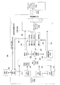
この点で、図1は、IOV-HC102を含む例示的なシステムオンチップ(SoC)100のブロック図である。図1の例では、IOV-HC102は、複数のI/Oクライアント104(0)〜104(N)が単一のフラッシュメモリベースのストレージデバイス106にアクセスすることを可能にするために提供される。いくつかの態様では、フラッシュメモリベースのストレージデバイス106は、非限定的な例として、ユニバーサルフラッシュストレージ(UFS)デバイス、または組込みマルチメディアカード(eMMC)デバイスを備え得る。特に、この態様では、フラッシュメモリベースのストレージデバイス106はモバイルデバイス内のSoC100に隣接して組み込まれているが、他の態様は、フラッシュメモリベースのストレージデバイス106をリムーバブルメモリデバイスとして採用した場合、同様の機能を達成し得る。
In this regard, FIG. 1 is a block diagram of an exemplary system on chip (SoC) 100 that includes an IOV-HC102. In the example of FIG. 1, IOV-
SoC100はまた、I/Oクライアント104(0)〜104(N)に仮想化機能と管理とを提供する仮想マシンマネージャ(VMM)108を含む。VMM108は、SoC100のプロセッサによって実行されるソフトウェアモジュールでもよく、必要または所望に応じてSoC100のシステムメモリ(図示せず)または他のメモリ位置に存在する。I/Oクライアント104(0)〜104(N)の各々は、SoC100のプロセッサ上、および/またはSoC100内のプロセッササブシステム(図示せず)上で実行される、ホストソフトウェアエンティティ(図1のI/Oクライアント104(0)およびI/Oクライアント104(1)など)を備え得る。IOV-HC102は、I/Oクライアント104(0)〜104(N)とフラッシュメモリベースのストレージデバイス106との間の仲介として作用し得る。このように、IOV-HC102は、フラッシュメモリベースのストレージデバイス106と通信しているのはI/Oクライアント104(0)〜104(N)だけであるかのように、I/Oクライアント104(0)〜104(N)が各々フラッシュメモリベースのストレージデバイス106と相互作用するように、I/Oクライアント104(0)〜104(N)とフラッシュメモリベースのストレージデバイス106との間の相互作用を制御し得る。同様に、IOV-HC102は、実際は複数のI/Oクライアント104(0)〜104(N)と通信しているときに、フラッシュメモリベースのストレージデバイス106が、単一のI/Oクライアント104(0)〜104(N)だけと通信しているかのように動作することを可能にするように構成され得る。
The
いくつかの態様による図1のIOV-HC102内の例示的な構成要素と通信フローとをより良く説明するために、図2が提供される。IOV-HC102は、使用されているフラッシュメモリベースのストレージデバイス106規格(たとえば、非限定的な例として、UFSまたはeMMC)のニーズに応じて、図2に示されるよりも多数または少数の要素を含み得ることを理解されたい。図2に見られるように、IOV-HC102は、それを通じて矢印202によって示されるように図1のVMM108がIOV-HC102と通信することができる、ベースレジスタインターフェース(BRI)200を含む。IOV-HC102はまた、クライアントレジスタインターフェース(CRI)204(0)〜204(N)を含む。CRI204(0)〜204(N)の各々は、CRI204(0)によってIOV-HC102に送信される要求206などの要求を送信するために、図1のI/Oクライアント104(0)〜104(N)のうちの1つに対応するためのインターフェースを表す。非限定的な例として、要求206は、転送要求(TR)および/またはタスク管理要求(TMR)を備え得る。本明細書に開示されるいくつかの態様によれば、要求206は、読出し要求、書込み要求、電力制御要求(たとえば、小型コンピュータシステムインターフェース(SCSI)START_STOP_UNIT(SSU)要求、またはeMMCスリープ要求)、および/または他の要求を備え得る。CRI204(0)〜204(N)はまた、クエリ要求またはノーオペレーション(NOP)命令など、他のタイプの要求またはコマンド206を送信するために使用され得る。
FIG. 2 is provided to better illustrate exemplary components and communication flows within the IOV-
図2に見られるように、CRI204(0)〜204(N)は、矢印210、212、および214によってそれぞれ示されるように、IOV-HC102の要求フェッチ回路(REQ FETCH CIRC)208に通信可能に結合されている。いくつかの態様では、要求フェッチ回路208は、UFSトランスポートプロトコル(UTP)転送要求記述子(UTRD)(図示せず)、またはeMMCタスク記述子(TD)などのトランスポートプロトコル記述子をシステムメモリ216からフェッチし、UTPコマンド記述子(UCD)(図示せず)などのコマンド記述子の位置を決定するためにトランスポートプロトコル記述子を復号する責任を負うことができる。次いで、要求フェッチ回路208は、矢印218によって示されるように、コマンド記述子のTRセクション(図示せず)をシステムメモリ216からフェッチし得る。
As seen in FIG. 2, CRIs 204 (0) -204 (N) can communicate to the request fetch circuit (REQ FETCH CIRC) 208 of the IOV-HC102, as indicated by
従来のUFSまたはeMMCホストコントローラでは、要求フェッチ回路208は、次にフェッチされた要求206からパラメータを抽出し、フェッチされた要求206全体を処理のためにトランスポートプロトコルエンジン220(たとえば、非限定的な例として、UTPエンジンまたはeMMCトランスポートプロトコルエンジン)に転送することになる。次いで、フェッチされた要求206は、相互接続222およびバス224を介して、フラッシュメモリベースのストレージデバイス106に送信され得る。しかしながら、マルチクライアント環境では、要求206の追加の検査および処理が必要とされる場合がある。たとえば、異なるタイプの要求206のためのカスタム処理を提供する、あるいはフェッチされた要求206をトラップおよび/または終了することが望ましい場合がある。
In a conventional UFS or eMMC host controller, the request fetch
したがって、IOV-HC102は、コマンドトラッピング機能を提供するように構成されている。したがって、IOV-HC102は、要求206を受信、検査、および処理するための要求フィルタ回路(REQ FILTER CIRCUIT)226と、コマンドトラッピングのための要求トラップ228と、I/Oクライアント104(0)〜104(N)への応答の送信を容易にするための応答生成回路230とを含み得る。要求フィルタ回路226、要求トラップ228、および応答生成回路230の動作は、以下でより詳細に説明される。
Accordingly, the IOV-HC102 is configured to provide a command trapping function. Accordingly, the IOV-
図2の参照を続けると、要求フェッチ回路208によってフェッチされたすべての要求206は、矢印232によって示されるように、IOV-HC102の要求フィルタ回路226によって受信される。要求フィルタ回路226は、要求206を検査および処理する責任を負う。具体的には、要求フィルタ回路226は、要求206の内容234に基づいて要求206が処理されるべき方法を決定する。非限定的な例として、UFS規格に基づくいくつかの態様では、要求フィルタ回路226は、要求206が処理されるべき方法を決定するために、要求206の内容234のトランザクションコード(TC)およびSCSIオペレーションコード(OPC)を検査し得る。同様に、eMMC規格に基づく態様では、要求フィルタ回路226は、要求206が処理されるべき方法を決定するために、要求206の内容234のコマンドインデックスとコマンド引数とを検査し得る。要求206の内容234に基づいて、要求フィルタ回路226は、要求206は処理のためにフラッシュメモリベースのストレージデバイス106に転送されるべきであると決定してもよく、要求206はトラップされるべきであると決定してもよい。その後、VMM108は、トラップされた要求206が修正されてフラッシュメモリベースのストレージ装置106に再発行されるべきかどうか、またはトラップされた要求206が終了されるべきかどうかを決定し得る。
Continuing with reference to FIG. 2, all
いくつかの態様では、要求フィルタ回路226は、要求206が、読出しコマンド、書込みコマンド、電力モード変更コマンド、または別のタイプのコマンドであるかどうかを決定するために、要求206の内容234を検査し得る。要求206の内容234が、要求206が読出しまたは書込みコマンドに対応することを示している場合、要求206は、矢印238によって示されるように、要求フィルタ回路226によってアクセス制御回路236に転送され得る。いくつかの態様によるアクセス制御回路236は、論理ユニット(図示せず)への読出し/書込みアクセスルールのハードウェア強制を提供する。その後、要求206がアクセス制御回路236によって検証される場合、矢印240によって示されるように、要求206はトランスポートプロトコルエンジン220に渡される。しかしながら、矢印242によって示されるように、アクセス制御回路236によって拒否された要求206は、ソフトウェア処理のためにトラップされる。要求206のトラッピングに関連付けられる動作は、以下でより詳細に説明される。
In some aspects, the
いくつかの態様によれば、要求206の内容234は、要求206が電力モード変更コマンドに対応することを示し得る。非限定的な例として、UFS規格に基づく態様では、内容234は、要求206がSCSI SSUコマンドであることを示し得、eMMC規格に基づく態様では、内容234は、要求206がeMMCスリープ(CMD5)コマンドであることを示し得る。その結果、フェッチされた要求206は、矢印246によって示されるように、要求フィルタ回路226によってMHPC244に送信され得る。いくつかの態様によるMHPC244は、フラッシュメモリベースのストレージデバイス106の電力モードを制御するために、図1のI/Oクライアント104(0)〜104(N)間の投票メカニズムを実装するハードウェアステートマシン(図示せず)を備える。フェッチされた要求206がMHPC244によって正常に処理されている場合、フェッチされた要求206は、矢印248によって示されるように、トランスポートプロトコルエンジン220に渡され得る。正常に処理されていない場合、MHPC244は静かにフェッチされた要求206を終了してもよく、矢印250によって示されるように、さらなる処理のためにフェッチされた要求206をトラップしてもよい。フェッチされた要求206が、読出しコマンド、書込みコマンド、または電力モード変更コマンド以外のコマンドに対応する場合、矢印252によって示されるように、要求フィルタ回路226はフェッチされた要求206を傍受して要求トラップ228内にトラップし得る。
According to some aspects, the
要求トラップ228は、要求206などのトラップされた要求を記憶するためにIOV-HC102によって提供される。いくつかの態様によれば、要求トラップ228内にはコマンドミラー(CM)254(0)〜254(N)があり、各々がCRI204(0)〜204(N)のうちの1つに関連付けられている。トラップされた要求206は、そこから要求206が受信される、対応するCRI204〜204(N)のCM254(0)〜254(N)に記憶され得る。いくつかの態様は、要求トラップ228が、要求206がトラップされることを示すために、BRI200を介してVMM108への割込み256を生成し得ることを提供し得る。次いで、VMM108は、情報を抽出するためにBRI200を介して適切なCM254(0)〜254(N)の内容を読み出すことによって、トラップされた要求206をさらに処理し得る。VMM108はまた、BRI200を介して、矢印260によって示されるように、応答生成回路230を使用して、発信しているCRI204(0)〜204(N)への応答258を生成するようにIOV-HC102に指示し得る。
Request trap 228 is provided by IOV-
いくつかの態様によれば、一旦要求206がトラップされると、要求フェッチ回路208はその処理を完了して、別のCRI204(0)〜204(N)のための次の要求206をフェッチするステップに進むことができる。トラップされた要求206がVMM108によって処理されるまで、トラップされた要求206に関連付けられるCRI204(0)〜204(N)のうちの特定のCRIが、要求フェッチアービトレーションから削除される。IOV-HC102に要求206を転送または廃棄するように指示することによってVMM108が要求206を処理するときのみ、CRI204(0)〜204(N)のうちの同じCRIからの後続の要求206は要求フェッチ回路208によってフェッチされ得る。
According to some aspects, once
トラップされた要求206を記憶するための、図2のIOV-HC102の要求トラップ228の例示的な構成要素を説明するために、図3が提供される。図3を説明する際に、明確化のために図1および図2の要素が参照される。図3に見られるように、要求トラップ228は、図2のCM254(0)〜254(N)を含み、それらの各々が図2のCRI204(0)〜204(N)のうちの1つに対応する。CM254(0)〜254(N)の各々は、対応するコマンドミラーステータスレジスタ(CMSR)300(0)〜300(N)と、コマンドミラーデータレジスタアレイ(CMDAT)302(0)〜302(N)とを提供する。要求トラップ228は、コマンドミラー制御レジスタ(CMCR)304をさらに含む。要求トラップ228の各例示的な要素の機能は、以下でより詳細に説明される。
FIG. 3 is provided to illustrate exemplary components of request trap 228 of IOV-
CMCR304は、要求トラップ228内にトラップされた要求206が処理されるべき方法についてIOV-HC102に指示するために、図2のVMM108によって使用され得るレジスタである。非限定的な例として、VMM108は、トラップされた要求206をトランスポートプロトコルエンジン220に渡すように、またはトラップされた要求206完全に終了するようにIOV-HC102に指示するために、CMCR304を介して処理命令306を送信し得る。いくつかの態様によれば、CMCR304はすべてのCM254(0)〜254(N)の間で共有される。
The CMCR 304 is a register that can be used by the
上述したように、要求206などのトラップされた要求は、そこから要求206が受信されるCRI204(0)〜204(N)に対応するCM254(0)〜254(N)に記憶され得る。トラップされた要求206の記憶を容易にするために、CM254(0)〜254(N)のCMSR300(0)〜300(N)の各々は、各トラップされた要求206に関する情報を表すそれぞれのステータス308(0)〜308(N)を記憶し得る。各ステータス308(0)〜308(N)は、いくつかの態様によれば、要求206に関連付けられるスロット番号(図示せず)および/または転送要求記述子(TRD)情報(図示せず)などのデータを備え得る。
As described above, a trapped request, such as
CM254(0)〜254(N)のCMDAT302(0)〜302(N)はレジスタアレイであり、それらの各々は、各トラップされた要求206の対応するプロトコル情報ユニット(PIU)310(0)〜310(N)を記憶するために使用され得る。いくつかの態様では、CMDAT302(0)〜302(N)の各々は、図2のCRI204(0)〜204(N)ごとに32バイトの空間を割り振ることができる。要求206が32バイトよりも大きい場合(たとえば、非限定的な例として、記述子書込みクエリ要求)、要求206の長さは対応するCMSR300(0)〜300(N)内に示され得る。次いで、VMM108は、システムメモリ216内のコマンド記述子アドレス(UFS規格に基づく態様における、UFSコマンド記述子(UCD)など)を計算し、システムメモリ216内の元の位置から直接要求206を読み出すことができる。
CMDAT 302 (0) -302 (N) of CM 254 (0) -254 (N) is a register array, each of which is associated with a corresponding protocol information unit (PIU) 310 (0)-for each trapped
図2に関して上述したように、IOV-HC102のいくつかの態様は、VMM108がIOV-HC102に、そこからトラップされた要求(要求206など)が発生するI/Oクライアント104(0)〜104(N)に送信されるべき応答258を生成するように指示することを可能にするために応答生成回路230を提供する。図2の応答生成回路230の一態様の例示的な要素を説明するために、図4が提供される。図4の説明において、明確化のために図1および図2の要素が参照される。
As described above with respect to FIG. 2, some aspects of the IOV-
図4に見られるように、応答生成回路230は、応答生成器制御レジスタ(RGCR)402と、応答生成器ステータスレジスタ(RGSR)404と、応答生成器PIUレジスタ(RGU)406とを備える。RGCR402は、いくつかの態様では、IOV-HC102に応答生成命令408を使用して応答258を送信するように指示するために、図2のVMM108によって使用され得る。非限定的な例として、応答生成命令408は、送信コマンド、応答送信方法、宛先CRI識別子、および/または全体的なコマンドステータス(OCS)を含み得る。応答生成回路230のRGSR404は、応答生成回路230のステータスに関するステータス410を記憶し得る。RGU406は、いくつかの態様では、I/Oクライアント104(0)〜104(N)のうちの1つに送信されるべき応答258の応答PIU412を記憶するための32バイトのレジスタ空間を備え得る。
As seen in FIG. 4, the response generation circuit 230 includes a response generator control register (RGCR) 402, a response generator status register (RGSR) 404, and a response generator PIU register (RGU) 406. RGCR 402 may be used by
応答生成回路230のいくつかの態様は、2つの応答送信方法のうちの1つまたは両方を提供し得る。いくつかの態様では、応答送信方法は、要求トラップ228によってRGU406に書き込まれている応答PIU412を備え得る。次いで、応答PIU412は、応答258が対象とされるI/Oクライアント104(0)〜104(N)のうちの1つのメモリ空間(図示せず)内のTRDで指定された位置にIOV-HC102によってコピーされ得る。あるいは、いくつかの態様は、VMM108は、I/Oクライアント104(0)〜104(N)のメモリ空間内の位置に直接応答PIU412を書き込むことができることを提供し得る。いずれかの送信技法の下で、VMM108は、I/Oクライアント104(0)〜104(N)のメモリ空間内のTRDにOCSフィールドを書き込むようにIOV-HC102に指示するために、およびI/Oクライアント104(0)〜104(N)によって要求されるように割込み256を生成するために、RGCR402を書き込むことができる。応答258が32バイト(たとえば、記述子読出しクエリ要求用)より大きいいくつかの態様では、VMM108は、I/Oクライアント104(0)〜104(N)のメモリ空間内の位置に直接応答PIU412を書き込むことができる。
Some aspects of the response generation circuit 230 may provide one or both of two response transmission methods. In some aspects, the response transmission method may comprise a response PIU 412 that is written to RGU 406 by request trap 228. The response PIU 412 then places the IOV-HC102 at the location specified by the TRD in one memory space (not shown) of the I / O clients 104 (0) -104 (N) for which the response 258 is intended. Can be copied by. Alternatively, some aspects may provide that the
UFS規格に基づく本明細書に開示されるいくつかの態様によれば、VMM108がRGCR402に書き込むとき、IOV-HC102は以下の例示的な動作を実行し得る。応答のコピーが必要な場合、IOV-HC102は、CRI識別子およびスロット番号から宛先アドレス(図示せず)を計算し得る。たとえば、UFS規格に基づく態様では、宛先アドレスは、UCDまたはUTPタスク管理要求記述子(UTMRD)の応答セクションに基づいて計算され得る。次いで、IOV-HC102は、RGU406から宛先アドレスに、応答PIU412の内容をコピーし得る。IOV-HC102は、UFS TRD (UTRD)またはUTMRD内の宛先アドレスにOCSを書き込む。IOV-HC102は、コマンド完了を示すために、適切なCRI204(0)〜204(N)にUTP転送要求リストドアベルレジスタ(UTRLDBR)、UTP転送要求リストクリアレジスタ(UTRLCLR)、および/またはUTPタスク管理要求リストドアベルレジスタ(UTMRLDBR)を設定する。次いで、IOV-HC102は、UTRDまたはUTMRDによって要求された場合、割込み256を生成し得る。eMMC規格に基づく本明細書に開示される態様では、応答PIU412は、VMM108によって適切なCRI204(0)〜204(N)の応答レジスタに書き込まれ、その後、VMM108はIOV-HC102に割込み256を生成するよう指示する。上述のUFSとeMMCとに基づく態様は、非限定的な例であることを理解されたい。
According to some aspects disclosed herein based on the UFS standard, when the
複数のI/Oクライアント104(0)〜104(N)にコマンドトラッピングを提供するために、図2のIOV-HC102の例示的な動作を説明するために、図5Aおよび図5Bが提供される。図5Aおよび図5Bを説明する際に、明確化のために図1、図2、および図4の要素が参照される。図5Aでは、動作は、IOV-HC102の要求フィルタ回路226が、複数のCRI204(0)〜204(N)のうちのCRI204(0)からフラッシュメモリベースのストレージデバイス106を対象とする要求206を受信することで開始する(ブロック500)。この点で、要求フィルタ回路226は、本明細書では「CRIからフラッシュメモリベースのストレージデバイスを対象とする要求を受信するための手段」と呼ばれ得る。要求フィルタ回路226は、要求206の内容234を検査する(ブロック502)。非限定的な例として、UFS規格に基づくいくつかの態様では、要求フィルタ回路226は、要求206の内容234のトランザクションコード(TC)とSCSIオペレーションコード(OPC)を検査し得、eMMC規格に基づく態様では、要求フィルタ回路226は、要求206の内容234のコマンドインデックスとコマンド引数とを検査し得る。したがって、要求フィルタ回路226は、本明細書では「要求の内容を検査するための手段」と呼ばれ得る。
To provide command trapping to multiple I / O clients 104 (0) -104 (N), FIGS. 5A and 5B are provided to illustrate exemplary operation of the IOV-
内容234に基づいて、要求フィルタ回路226は、要求206が処理のためにフラッシュメモリベースのストレージデバイス106に転送されるべきかどうか、または要求206が要求トラップ228内にトラップされるべきどうかを決定する(ブロック504)。したがって、要求フィルタ回路226は、本明細書では「要求が処理のためにフラッシュメモリベースのストレージデバイスに転送されるべきか、またはトラップされるべきかどうかを決定するための手段」と呼ばれ得る。決定ブロック504で、要求フィルタ回路226が要求206は転送されるべきであると決定した場合、要求フィルタ回路226は要求206をフラッシュメモリベースのストレージデバイス106に転送する(ブロック506)。この点で、要求フィルタ回路226は、本明細書では「要求をフラッシュメモリベースのストレージデバイスに転送するための手段」と呼ばれ得る。決定ブロック504で、要求フィルタ回路226が要求206はトラップされるべきであると決定した場合、要求フィルタ回路226は要求206を要求トラップ228内にトラップする(ブロック508)。したがって、要求フィルタ回路226は、本明細書では「要求を要求トラップ内にトラップするための手段」と呼ばれ得る。図6に関して以下でより詳細に記述されるように、いくつかの態様は、要求206を転送またはトラップする決定は、内容234で示されるように、要求206のタイプに基づき得ることを提供し得る。次いで、処理が図5Bのブロック510で再開する。
Based on
次に図5Bを参照すると、いくつかの態様では、IOV-HC102の応答生成回路230は、要求206のトラッピングに応答して、VMM108から応答258を受信し得る(ブロック510)。この点で、応答生成回路230は、本明細書では「要求をトラップすることへの応答を受信するための手段」と呼ばれ得る。応答生成回路230は、応答生成回路230のRGU406に応答258の応答PIU412を記憶し得る(ブロック512)。したがって、応答生成回路230は、本明細書では「RGPIUに応答を記憶するための手段」と呼ばれ得る。次いで、IOV-HC102は、応答生成回路230のRGCR402を介してVMM108から応答生成命令408を受信し得る(ブロック514)。したがって、IOV-HC102は、本明細書では「RGCRを介してVMMから応答生成命令を受信するための手段」と呼ばれ得る。いくつかの態様(たとえば、eMMC規格に基づく態様)では、RGCR402は採用されない場合があり、したがって、ブロック514の任意の動作が省略され得る。
Referring now to FIG. 5B, in some aspects, the response generation circuit 230 of the IOV-
図6は、受信された要求が処理および/またはトラップされ得る方法を決定するための、図2のIOV-HC102の例示的な動作を示すフローチャートである。図6を説明する際に、明確化のために図1および図2の要素が参照される。いくつかの態様では、図6に示されるいくつかの動作は、要求206が処理のためにフラッシュメモリベースのストレージデバイス106に転送されるべきかどうか、または要求206が要求トラップ228内にトラップされるべきかどうかを決定するために、図5Aのブロック504の動作に対応し得る。
FIG. 6 is a flowchart illustrating an exemplary operation of the IOV-
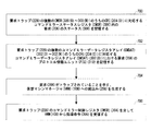
図6の動作は、要求フィルタ回路226が、内容234が、要求206は、読出しコマンド、書込みコマンド、または電力モード変更コマンドのうちの1つであることを示すかどうかを決定することで開始する(ブロック600)。ブロック600で、要求206が、読出しコマンドまたは書込みコマンドと決定された場合、要求206はIOV-HC102のアクセス制御回路236に渡され得、要求206が有効であるかどうかを決定する(ブロック602)。この点で、アクセス制御回路236は、本明細書では「要求が有効であるかどうかを決定するための手段」と呼ばれ得る。ブロック602で、要求206が有効であると決定された場合、要求206がフラッシュメモリベースのストレージデバイス106に転送される(ブロック604)。ブロック602で、アクセス制御回路236によって要求206は有効ではないと決定された場合、要求206は要求トラップ228内にトラップされる(ブロック606)。
The operation of FIG. 6 begins with the
決定ブロック600で、要求フィルタ回路226が、要求206は電力モード変更コマンドであると決定されたと決定した場合、処理のために、要求206がIOV-HC102のMHPC244に転送される(ブロック608)。したがって、要求フィルタ回路226は、本明細書では「処理のために要求をIOV-HCのMHPCに転送するための手段」と呼ばれ得る。次いで、MHPC244によって要求206が正常に処理されたかどうかに関して決定が行われる(ブロック610)。したがって、MHPC244は、本明細書では「MHPCによって要求が正常に処理されたかどうかを決定するための手段」と呼ばれ得る。MHPC244が要求206を正常に処理した場合、MHPC244は、要求206をフラッシュメモリベースのストレージデバイス106に渡すか、MHPC244の内部ロジックに基づいて要求206を終了する(ブロック612)。MHPC244によって要求206が正常に処理されていない場合、要求206は要求トラップ228内にトラップされる(ブロック614)。決定ブロック600に戻って、要求206が、読出しコマンド、書込みコマンド、または電力モード変更コマンドではないと決定された場合、要求206は要求トラップ228内にトラップされる(ブロック616)。したがって、要求フィルタ回路226は、「内容が、要求は読出しコマンド、書込みコマンド、または電力モード変更コマンドのうちの1つではないという決定に応答して、要求を要求トラップ内にトラップするための手段」と呼ばれ得る。
If, at
図2の要求トラップ228を使用するコマンドトラッピングのためのいくつかの態様におけるIOV-HC102の例示的な動作をさらに説明するために、図7が提供される。図7を説明する際に、明確化のために図1〜図3の要素が参照される。図7における動作は、要求トラップ228が、要求206のステータス308を要求トラップ228の複数のCMSR300(0)〜300(N)のうちのCRI204(0)に対応するCMSR300に記憶することで開始する(ブロック700)。この点で、要求トラップ228は、本明細書では「要求のステータスをCRIに対応するCMSRに記憶するための手段」と呼ばれ得る。要求トラップ228はまた、要求206のPIU310(0)を、要求トラップ228の複数のCMDAT302(0)〜302(N)のうちのCRI204(0)に対応するCMDAT302(0)に記憶する(ブロック702)。したがって、要求トラップ228は、本明細書では「要求のPIUをCRIに対応するCMDATに記憶するための手段」と呼ばれ得る。次に、要求トラップ228は、要求206がトラップされていることを示す、VMM108への割込み256を生成し得る(ブロック704)。したがって、要求トラップ228は、本明細書では「要求がトラップされることを示すVMMへの割込みを生成するための手段」と呼ばれ得る。次いで、IOV-HC102は、要求トラップ228のCMCR304を介してVMM108から処理命令306を受信し得る(ブロック706)。この点で、IOV-HC102は、本明細書では「要求トラップのCMCRを介してVMMから処理命令を受信するための手段」と呼ばれ得る。これは、図7に示される例示的な動作は、eMMC規格に基づく態様などの、本明細書に開示されるいくつかの態様に適用されない場合があることを理解されたい。
To further illustrate exemplary operation of the IOV-
本明細書に開示される態様による、フラッシュメモリベースのストレージデバイスのIOV-HCにおけるコマンドトラッピングは、任意のプロセッサベースのデバイスに提供または統合され得る。例としては、限定するものではないが、セットトップボックス、エンターテイメントユニット、ナビゲーションデバイス、通信デバイス、固定ロケーションデータユニット、モバイルロケーションデータユニット、モバイル電話、セルラー電話、コンピュータ、ポータブルコンピュータ、デスクトップコンピュータ、携帯情報端末(PDA)、モニタ、コンピュータモニタ、テレビ、チューナ、ラジオ、衛星ラジオ、音楽プレーヤ、デジタル音楽プレーヤ、ポータブル音楽プレーヤ、デジタルビデオプレーヤ、ビデオプレーヤ、デジタルビデオディスク(DVD)プレーヤ、およびポータブルデジタルビデオプレーヤを含む。 Command trapping in the IOV-HC of a flash memory based storage device according to aspects disclosed herein may be provided or integrated into any processor based device. Examples include, but are not limited to, set-top boxes, entertainment units, navigation devices, communication devices, fixed location data units, mobile location data units, mobile phones, cellular phones, computers, portable computers, desktop computers, portable information Terminal (PDA), monitor, computer monitor, television, tuner, radio, satellite radio, music player, digital music player, portable music player, digital video player, video player, digital video disc (DVD) player, and portable digital video player including.
この点で、図8は、図1のIOV-HC102とともにSoC100を採用し得るプロセッサベースのシステム800の一例を示す。この例では、プロセッサベースのシステム800は1つまたは複数の中央処理装置(CPU)802を含み、各々が1つまたは複数のプロセッサ804を含む。CPU802は、一時的に記憶されたデータへの迅速なアクセスのためにプロセッサ804に結合されたキャッシュメモリ806を有し得る。CPU802はシステムバス808に結合され、プロセッサベースのシステム800に含まれるデバイスを相互に連結し得る。よく知られているように、CPU802は、システムバス808を介してアドレス、制御、およびデータ情報を交換することによって、これらの他のデバイスと通信する。たとえば、CPU802は、スレーブデバイスの一例として、メモリコントローラ810にバストランザクション要求を通信し得る。図8に示されていないが、複数のシステムバス808を設けることができる。
In this regard, FIG. 8 shows an example of a processor-based
他のデバイスがシステムバス808に接続され得る。図8に示されるように、これらのデバイスは、例として、メモリシステム812、1つまたは複数の入力デバイス814、1つまたは複数の出力デバイス816、1つまたは複数のネットワークインターフェースデバイス818、および1つまたは複数のディスプレイコントローラ820を含み得る。入力デバイス814は、限定はしないが、入力キー、スイッチ、音声プロセッサ等を含む、任意のタイプの入力デバイスを含み得る。出力デバイス816は、限定はしないが、音声、ビデオ、他の視覚インジケータ等を含む、任意のタイプの出力デバイスを含み得る。ネットワークインターフェースデバイス818は、ネットワーク822への、またはそこからのデータの交換を可能にするように構成された任意のデバイスであり得る。ネットワーク822は、限定はしないが、ワイヤードまたはワイヤレスネットワーク、プライベートまたはパブリックネットワーク、ローカルエリアネットワーク(LAN)、ワイドローカルエリアネットワーク、ワイヤレスローカルエリアネットワーク、BLUETOOTH(登録商標)(BT)、およびインターネットを含む、任意のタイプのネットワークであり得る。ネットワークインターフェースデバイス818は、任意のタイプの所望の通信プロトコルをサポートするように構成され得る。メモリシステム812は、1つまたは複数のメモリユニット824(0)〜824(N)を含み得る。
Other devices may be connected to the system bus 808. As shown in FIG. 8, these devices include, by way of example, a
CPU802はまた、1つまたは複数のディスプレイ826に送信された情報を制御するために、システムバス808を介してディスプレイコントローラ820にアクセスするように構成され得る。ディスプレイコントローラ820は、1つまたは複数のビデオプロセッサ828を介して表示されるべき情報をディスプレイ826に送信して、ディスプレイ826に適した形式に表示されるべき情報を処理する。ディスプレイ826は、限定はしないが、陰極線管(CRT)、液晶ディスプレイ(LCD)、発光ダイオード(LED)ディスプレイ、プラズマディスプレイ等の任意のタイプのディスプレイを含み得る。
当業者は、本明細書に開示された態様に関連して説明される様々な例示的な論理ブロック、モジュール、回路、およびアルゴリズムは、電子ハードウェア、メモリまたは別のコンピュータ可読媒体に記憶された命令として実装され得、プロセッサまたは他の処理デバイス、あるいはその両方の組合せによって実行されることをさらに理解するだろう。本明細書に記載されたデバイスは、例として、任意の回路、ハードウェア構成要素、集積回路(IC)、またはICチップで採用され得る。本明細書において開示されるメモリは、任意のタイプおよびサイズのメモリとすることができ、所望の任意のタイプの情報を記憶するように構成され得る。この互換性を明示的に説明するために、様々な例示的な構成要素、ブロック、モジュール、回路、およびステップが、それらの機能の観点から一般的に上述されている。そのような機能がどのように実現されるかは、特定の用途、設計上の選択、および/または、システム全体に課された設計上の制約によって決まる。当業者は、説明された機能を特定の用途ごとに様々な方法で実装することができるが、そのような実装の決定は、本開示の範囲からの逸脱を引き起こすものと解釈されるべきではない。 Those skilled in the art will recognize that the various exemplary logic blocks, modules, circuits, and algorithms described in connection with the aspects disclosed herein are stored in electronic hardware, memory, or another computer-readable medium. It will be further appreciated that it may be implemented as instructions and executed by a processor or other processing device, or a combination of both. The devices described herein can be employed by way of example in any circuit, hardware component, integrated circuit (IC), or IC chip. The memory disclosed herein can be any type and size of memory and can be configured to store any type of information desired. To explicitly illustrate this compatibility, various exemplary components, blocks, modules, circuits, and steps are generally described above in terms of their functionality. How such functionality is achieved depends on the particular application, design choices, and / or design constraints imposed on the overall system. Those skilled in the art can implement the described functionality in a variety of ways for each particular application, but such implementation decisions should not be construed as causing deviations from the scope of this disclosure. .
本明細書に開示された態様に関連して説明される様々な例示的な論理ブロック、モジュール、および回路は、プロセッサ、デジタル信号プロセッサ(DSP)、特定用途向け集積回路(ASIC)、フィールドプログラマブルゲートアレイ(FPGA)または他のプログラマブル論理デバイス、ディスクリートゲートまたはトランジスタロジック、ディスクリートハードウェア構成要素、あるいは本明細書に記載の機能を実行するように設計されたそれらの任意の組合せで実装または実行され得る。プロセッサはマイクロプロセッサであり得るが、代替実施形態では、プロセッサは、任意の従来型プロセッサ、コントローラ、マイクロコントローラ、またはステートマシンであり得る。プロセッサはまた、コンピューティングデバイスの組合せ、たとえばDSPとマイクロプロセッサの組合せ、複数のマイクロプロセッサ、1つまたは複数のマイクロプロセッサとDSPコア、あるいは任意の他のそのような構成として実装され得る。 Various exemplary logic blocks, modules, and circuits described in connection with the aspects disclosed herein are processors, digital signal processors (DSPs), application specific integrated circuits (ASICs), field programmable gates. May be implemented or implemented in an array (FPGA) or other programmable logic device, discrete gate or transistor logic, discrete hardware components, or any combination thereof designed to perform the functions described herein. . The processor can be a microprocessor, but in alternative embodiments, the processor can be any conventional processor, controller, microcontroller, or state machine. The processor may also be implemented as a combination of computing devices, such as a combination of DSP and microprocessor, multiple microprocessors, one or more microprocessors and DSP cores, or any other such configuration.
本明細書に開示された態様は、ハードウェアにおいて、およびハードウェアに記憶された命令において具体化され得、たとえば、ランダムアクセスメモリ(RAM)、フラッシュメモリ、読出し専用メモリ(ROM)、電気的プログラマブルROM(EPROM)、電気的消去可能プログラマブルROM(EEPROM)、レジスタ、ハードディスク、リムーバブルディスク、CD-ROM、または当技術分野で知られているコンピュータ可読媒体の他の任意の形態に存在し得る。例示的な記憶媒体は、プロセッサが記憶媒体から情報を読み取り、記憶媒体に情報を書き込むことができるようにプロセッサに結合される。代替として、記憶媒体はプロセッサと一体構成であってもよい。プロセッサおよび記憶媒体はASIC内に存在し得る。ASICは、遠隔局に存在し得る。代替として、プロセッサおよび記憶媒体は、遠隔局、基地局、またはサーバにおけるディスクリート構成要素として存在し得る。 Aspects disclosed herein may be embodied in hardware and in instructions stored in hardware, such as random access memory (RAM), flash memory, read only memory (ROM), electrically programmable It can be in ROM (EPROM), electrically erasable programmable ROM (EEPROM), register, hard disk, removable disk, CD-ROM, or any other form of computer readable medium known in the art. An exemplary storage medium is coupled to the processor such that the processor can read information from, and write information to, the storage medium. In the alternative, the storage medium may be integral to the processor. The processor and the storage medium can reside in an ASIC. The ASIC can reside at a remote station. In the alternative, the processor and the storage medium may reside as discrete components in a remote station, base station, or server.
また、本明細書の例示的な態様のいずれかに記載の動作ステップは、実施例および説明を提供するために記載されていることに留意されたい。説明した動作は、図示した順序以外の多数の異なる順序で実行され得る。さらに、単一の動作ステップで説明した動作は、実際にはいくつかの異なるステップで実行され得る。さらに、例示的な態様で説明した1つまたは複数の動作ステップが組み合わされ得る。当業者には容易に明らかになるように、フローチャート図に示す動作ステップは、多数の異なる修正を受ける場合があることを理解されたい。当業者はまた、情報および信号が、様々な異なる技術および技法のいずれかを用いて表され得ることを理解するだろう。たとえば、上記の説明全体にわたって言及され得るデータ、命令、コマンド、情報、信号、ビット、シンボル、およびチップは、電圧、電流、電磁波、磁場もしくは磁性粒子、光場または光学粒子、またはそれらの任意の組合せによって表され得る。 It should also be noted that the operational steps described in any of the exemplary aspects herein are set forth to provide examples and explanations. The operations described can be performed in a number of different orders other than the order shown. Furthermore, the operations described in a single operation step may actually be performed in several different steps. Further, one or more operational steps described in the exemplary aspects may be combined. It should be understood that the operational steps shown in the flowchart diagrams may be subject to many different modifications, as will be readily apparent to those skilled in the art. Those skilled in the art will also understand that information and signals may be represented using any of a variety of different technologies and techniques. For example, data, instructions, commands, information, signals, bits, symbols, and chips that may be referred to throughout the above description are voltages, currents, electromagnetic waves, magnetic or magnetic particles, optical or optical particles, or any of them Can be represented by a combination.
本開示の前の説明は、当業者が本開示を作成または使用することを可能にするために提供される。本開示に対する様々な修正は当業者には容易に明らかになり、本明細書で定義された一般的な原理は、本開示の趣旨または範囲から逸脱することなしに他の変形形態に適用され得る。したがって、本開示は、本明細書で説明する例および設計に限定されるものではなく、本明細書で開示する原理および新規の特徴と一致する最も広い範囲を与えられるべきである。 The previous description of the disclosure is provided to enable any person skilled in the art to make or use the disclosure. Various modifications to the present disclosure will be readily apparent to those skilled in the art, and the generic principles defined herein may be applied to other variations without departing from the spirit or scope of the disclosure. . Accordingly, the present disclosure is not limited to the examples and designs described herein, but is to be accorded the widest scope consistent with the principles and novel features disclosed herein.
100 システムオンチップ(SoC)
102 IOV-HC
104(0)〜104(N) I/Oクライアント
106 フラッシュメモリベースのストレージデバイス
108 仮想マシンマネージャ(VMM)
200 ベースレジスタインターフェース(BRI)
204(0)〜204(N) クライアントレジスタインターフェース(CRI)、VLCI
206 コマンド
206 フェッチされた要求
206 トラップされた要求
208 要求フェッチ回路
210 矢印
212 矢印
214 矢印
216 システムメモリ
218 矢印
220 トランスポートプロトコルエンジン
222 相互接続
224 バス
226 要求フィルタ回路
228 要求トラップ
230 応答生成回路
232 矢印
234 内容
236 アクセス制御回路
240 矢印
242 矢印
244 MHPC
246 矢印
248 矢印
250 矢印
252 矢印
254(0)〜254(N) コマンドミラー
256 割込み
258 応答
260 矢印
300(0)〜300(N) コマンドミラーステータスレジスタ(CMSR)
302(0)〜302(N) コマンドミラーデータレジスタアレイ(CMDAT)
304 コマンドミラー制御レジスタ(CMCR)
306 処理命令
308(0)〜308(N) ステータス
402 応答生成器制御レジスタ(RGCR)
404 応答生成器ステータスレジスタ(RGSR)
406 応答生成器PIUレジスタ(RGU)
408 応答生成命令
410 ステータス
412 応答PIU
800 プロセッサベースのシステム
802 中央処理装置(CPU)
804 プロセッサ
806 キャッシュメモリ
808 システムバス
810 メモリコントローラ
812 メモリシステム
814 入力デバイス
816 出力デバイス
818 ネットワークインターフェースデバイス
820 ディスプレイコントローラ
822 ネットワーク
824(1)〜824(N) メモリユニット
826 ディスプレイ
828 ビデオプロセッサ
100 system on chip (SoC)
102 IOV-HC
104 (0) to 104 (N) I / O client
106 Flash memory based storage devices
108 Virtual Machine Manager (VMM)
200 Base register interface (BRI)
204 (0) to 204 (N) Client register interface (CRI), VLCI
206 commands
206 Request fetched
206 trapped request
208 Request fetch circuit
210 arrow
212 arrow
214 arrows
216 system memory
218 arrow
220 Transport Protocol Engine
222 interconnect
224 bus
226 Request filter circuit
228 Request trap
230 Response generation circuit
232 arrows
234 Contents
236 Access control circuit
240 arrows
242 arrow
244 MHPC
246 arrow
248 arrow
250 arrows
252 arrow
254 (0) to 254 (N) Command mirror
256 interrupts
258 responses
260 arrows
300 (0) to 300 (N) Command mirror status register (CMSR)
302 (0) to 302 (N) Command mirror data register array (CMDAT)
304 Command mirror control register (CMCR)
306 Processing instruction
308 (0) to 308 (N) status
402 Response generator control register (RGCR)
404 Response generator status register (RGSR)
406 Response generator PIU register (RGU)
408 Response generation command
410 status
412 Response PIU
800 processor-based system
802 Central processing unit (CPU)
804 processor
806 cache memory
808 system bus
810 Memory controller
812 memory system
814 input device
816 output device
818 network interface device
820 display controller
822 network
824 (1) to 824 (N) Memory unit
826 display
828 video processor
Claims (16)
対応する複数のクライアントレジスタインターフェース(CRI)を介して複数の入力/出力(I/O)クライアントに、およびフラッシュメモリベースのストレージデバイスに通信可能に結合された入力/出力仮想化(IOV)ホストコントローラ(HC)(IOV-HC)であって、
前記IOV-HCが要求トラップを備え、
前記IOV-HCが、
前記IOV-HCの要求フィルタ回路によって、前記複数のCRIのうちの1つのCRIから前記フラッシュメモリベースのストレージデバイスを対象とする要求を受信することと、
前記要求フィルタ回路によって、前記要求の内容を検査することと、
前記要求フィルタ回路によって、前記内容に基づいて、前記要求が処理のために前記フラッシュメモリベースのストレージデバイスに転送されるべきか、またはトラップされるべきかどうかを決定することであって、前記要求フィルタ回路が、前記要求が読出しコマンド、書込みコマンド、または電力モード変更コマンドのうちの1つであることを前記内容が示しているかどうかを決定するように構成される、決定することと、
処理のために、前記要求が前記フラッシュメモリベースのストレージデバイスに転送されるべきであるという決定に応答して、前記要求を前記フラッシュメモリベースのストレージデバイスに転送することと、
前記要求がトラップされるべきであるという決定に応答して、前記要求を前記要求トラップ内にトラップすることと
前記要求フィルタ回路による、前記要求が前記読出しコマンドまたは前記書込みコマンドのうちの1つであることを前記内容が示すという決定に応答して、前記IOV-HCのアクセス制御回路によって、前記要求が有効であるかどうかを決定することと、
前記要求が有効であるという決定に応答して、前記要求を前記フラッシュメモリベースのストレージデバイスに転送することと、
前記要求が有効ではないという決定に応答して、前記要求を前記要求トラップ内にトラップすることと
を行うように構成される、IOV-HC。 Input / output virtualization (IOV) host controller (HC) (IOV-HC),
Input / output virtualization (IOV) host controller communicatively coupled to multiple input / output (I / O) clients and to flash memory-based storage devices via corresponding multiple client register interfaces (CRI) (HC) (IOV-HC),
The IOV-HC is equipped with a request trap ,
Before Symbol IOV-HC is,
And that the request filter circuit before Symbol IOV-HC, receives the request shall be the subject of storage devices of the flash memory base from one of the CRI of the plurality of CRI,
Inspecting the content of the request by the request filter circuit;
Determining whether the request should be forwarded or trapped to the flash memory based storage device for processing by the request filter circuit based on the content, the request filter circuit; Determining, wherein a filter circuit is configured to determine whether the content indicates that the request is one of a read command, a write command, or a power mode change command ;
Transferring the request to the flash memory-based storage device in response to a determination that the request should be transferred to the flash memory-based storage device for processing;
In response to a determination that the request should be trapped, trapping the request in the request trap;
In response to the request filtering circuit determining that the content indicates that the request is one of the read command or the write command, the request is validated by the IOV-HC access control circuit. Determining whether or not
In response to a determination that the request is valid, transferring the request to the flash memory-based storage device;
An IOV-HC configured to trap the request in the request trap in response to a determination that the request is not valid .
コマンドミラー制御レジスタ(CMCR)と、Command mirror control register (CMCR)
複数のコマンドミラー(CM)とを備え、前記複数のコマンドミラー(CM)の各々が、A plurality of command mirrors (CM), each of the plurality of command mirrors (CM),
複数のコマンドミラーステータスレジスタ(CMSR)であって、各々が前記複数のCRIのうちの1つのCRIに対応するコマンドミラーステータスレジスタ(CMSR)と、A plurality of command mirror status registers (CMSR), each of which corresponds to one CRI of the plurality of CRIs, and a command mirror status register (CMSR),
複数のコマンドミラーデータレジスタアレイ(CMDAT)であって、各々が前記複数のCRIのうちの1つのCRIに対応するコマンドミラーデータレジスタアレイとA plurality of command mirror data register arrays (CMDAT) each having a command mirror data register array corresponding to one CRI of the plurality of CRIs;
を備え、With
前記IOV-HCが、The IOV-HC is
要求のステータスを前記複数のCMSRのうちの前記CRIに対応するCMSRに記憶することと、Storing the status of the request in a CMSR corresponding to the CRI of the plurality of CMSRs;
前記要求のプロトコル情報ユニット(PIU)を前記複数のCMDATのうちの前記CRIに対応するCMDATに記憶することと、Storing the requested protocol information unit (PIU) in a CMDAT corresponding to the CRI of the plurality of CMDATs;
前記要求がトラップされることを示す仮想マシンマネージャ(VMM)への割込みを生成することと、Generating an interrupt to a virtual machine manager (VMM) indicating that the request is trapped;
前記CMCRを介して前記VMMから処理命令を受信することとReceiving processing instructions from the VMM via the CMCR;
を行うように構成されることによって、前記要求を前記要求トラップ内にトラップするように構成される、請求項1に記載のIOV-HC。The IOV-HC of claim 1, wherein the IOV-HC is configured to trap the request in the request trap.
応答生成器プロトコル情報ユニット(RGPIU)とを備える応答生成回路をさらに備え、
前記IOV-HCが、前記要求を前記要求トラップ内にトラップすることに応答して、
前記応答生成回路によって、前記要求をトラップすることへの応答を受信することと、
前記応答のPIUを前記RGPIUに記憶することと、
前記RGCRを介してVMMから応答生成命令を受信することと
を行うようにさらに構成される、請求項1に記載のIOV-HC。 Response generator control register (RGCR),
A response generator circuit comprising a response generator protocol information unit (RGPIU),
In response to the IOV-HC trapping the request in the request trap,
Receiving a response to trapping the request by the response generation circuit;
Storing the PIU of the response in the RGPIU;
The IOV-HC of claim 1, further configured to receive a response generation command from a VMM via the RGCR.
前記要求を、処理のために前記IOV-HCのマルチホスト電力コントローラ(MHPC)に転送することと、
前記MHPCによって前記要求が正常に処理されたかどうかを決定することと
を行うようにさらに構成され、
前記IOV-HCが、前記MHPCによって前記要求が正常に処理されなかったという決定に応答して、前記要求を前記要求トラップ内にトラップするように構成される、請求項1に記載のIOV-HC。 In response to a determination by the request filter circuit that the content indicates that the request is the power mode change command,
Forwarding the request to the IOV-HC multi-host power controller (MHPC) for processing;
Further configured to determine whether the request has been successfully processed by the MHPC;
The IOV-HC of claim 1 , wherein the IOV-HC is configured to trap the request in the request trap in response to a determination that the request was not successfully processed by the MHPC. .
入力/出力仮想化(IOV)ホストコントローラ(HC)(IOV-HC)の要求フィルタ回路によって、複数のクライアントレジスタインターフェース(CRI)のうちの1つのCRIから前記フラッシュメモリベースのストレージデバイスを対象とする要求を受信するステップと、
前記要求フィルタ回路によって、前記要求の内容を検査するステップと、
前記要求フィルタ回路によって、前記要求が読出しコマンド、書込みコマンド、および電力モード変更コマンドのうちの1つであることを前記内容が示すかどうかを決定することによって、前記内容に基づいて、前記要求が処理のために前記フラッシュメモリベースのストレージデバイスに転送されるべきか、または要求トラップ内にトラップされるべきかどうかを決定するステップと、
処理のために、前記要求が前記フラッシュメモリベースのストレージデバイスに転送されるべきであるという決定に応答して、前記要求を前記フラッシュメモリベースのストレージデバイスに転送するステップと、
前記要求がトラップされるべきであるという決定に応答して、前記要求を前記要求トラップ内にトラップするステップと
前記要求が前記読出しコマンドまたは前記書込みコマンドのうちの1つであることを前記内容が示すという決定に応答して、前記IOV-HCのアクセス制御回路によって、前記要求が有効であるかどうかを決定するステップと
を備え、
前記要求を前記フラッシュメモリベースのストレージデバイスに転送するステップが、前記要求が有効であるという決定に応答し、
前記要求を前記要求トラップ内にトラップするステップが、前記要求が有効ではないという決定に応答する、方法。 A method for providing command trapping to a flash memory based storage device for multiple hosts, comprising:
Input / output virtualization (IOV) Host controller (HC) (IOV-HC) request filter circuit targets the flash memory-based storage device from one CRI of multiple client register interfaces (CRI) Receiving a request; and
Inspecting the content of the request by the request filter circuit;
Based on the content, the request is determined by determining whether the content indicates that the request is one of a read command, a write command, and a power mode change command by the request filter circuit. Determining whether to be transferred to the flash memory based storage device for processing or to be trapped in a request trap;
Transferring the request to the flash memory based storage device in response to a determination that the request should be transferred to the flash memory based storage device for processing;
In response to a determination that the request should be trapped, trapping the request in the request trap;
In response to a determination that the content indicates that the request is one of the read command or the write command, the IOV-HC access control circuit determines whether the request is valid. A step and <br/>
Transferring the request to the flash memory-based storage device in response to a determination that the request is valid;
The method of trapping the request in the request trap is responsive to a determination that the request is not valid .
前記要求のステータスを、前記要求トラップの複数のコマンドミラーステータスレジスタ(CMSR)のうちの前記CRIに対応するCMSRに記憶するステップと、Storing the status of the request in a CMSR corresponding to the CRI of a plurality of command mirror status registers (CMSR) of the request trap;
前記要求のプロトコル情報ユニット(PIU)を、前記要求トラップの複数のコマンドミラーデータレジスタアレイ(CMDAT)のうちの前記CRIに対応するCMDATに記憶するステップと、Storing the protocol information unit (PIU) of the request in a CMDAT corresponding to the CRI in a plurality of command mirror data register arrays (CMDAT) of the request trap;
前記要求がトラップされることを示す仮想マシンマネージャ(VMM)への割込みを生成するステップと、Generating an interrupt to a virtual machine manager (VMM) indicating that the request is trapped;
前記要求トラップのコマンドミラー制御レジスタ(CMCR)を介して前記VMMから処理命令を受信するステップとReceiving a processing instruction from the VMM via a command mirror control register (CMCR) of the request trap; and
を備える、請求項10に記載の方法。The method of claim 10, comprising:
応答生成回路によって、前記要求をトラップすることへの応答を受信するステップと、
前記応答を前記応答生成回路の応答生成器プロトコル情報ユニット(RGPIU)に記憶するステップと、
前記応答生成回路の応答生成器制御レジスタ(RGCR)を介してVMMから応答生成命令を受信するステップと
をさらに備える、請求項10に記載の方法。 In response to trapping the request in the request trap,
Receiving a response to trapping the request by a response generation circuit;
Storing the response in a response generator protocol information unit (RGPIU) of the response generation circuit;
Further comprising receiving a response generation command from V MM via the response generator control register of the response generating circuit (rGCR), The method of claim 10.
前記要求を、処理のために前記IOV-HCのマルチホスト電力コントローラ(MHPC)に転送するステップと、
前記MHPCによって前記要求が正常に処理されたかどうかを決定するステップと
をさらに備え、
前記要求を前記要求トラップ内にトラップするステップが、前記MHPCによって前記要求が正常に処理されなかったという決定に応答する、請求項10に記載の方法。 In response to a determination by the request filter circuit that the content indicates that the request is the power mode change command,
Forwarding the request to the IOV-HC multi-host power controller (MHPC) for processing;
Determining whether the request has been successfully processed by the MHPC;
The step of trapping the request in the request trap, the request is in response to a determination that has not been successfully processed by said MHPC, The method of claim 10.
Applications Claiming Priority (5)
| Application Number | Priority Date | Filing Date | Title |
|---|---|---|---|
| US201462007123P | 2014-06-03 | 2014-06-03 | |
| US62/007,123 | 2014-06-03 | ||
| US14/728,400 | 2015-06-02 | ||
| US14/728,400 US9690720B2 (en) | 2014-06-03 | 2015-06-02 | Providing command trapping using a request filter circuit in an input/output virtualization (IOV) host controller (HC) (IOV-HC) of a flash-memory-based storage device |
| PCT/US2015/033970 WO2015187824A1 (en) | 2014-06-03 | 2015-06-03 | Command trapping in an input/output virtualization (iov) host controller (hc) (iov-hc) of a flash-memory-based storage device |
Publications (3)
| Publication Number | Publication Date |
|---|---|
| JP2017518574A JP2017518574A (en) | 2017-07-06 |
| JP2017518574A5 JP2017518574A5 (en) | 2017-09-21 |
| JP6231704B2 true JP6231704B2 (en) | 2017-11-15 |
Family
ID=54701761
Family Applications (1)
| Application Number | Title | Priority Date | Filing Date |
|---|---|---|---|
| JP2016570297A Expired - Fee Related JP6231704B2 (en) | 2014-06-03 | 2015-06-03 | Command trapping in input / output virtualization (IOV) host controller (HC) (IOV-HC) of flash memory based storage devices |
Country Status (6)
| Country | Link |
|---|---|
| US (1) | US9690720B2 (en) |
| EP (1) | EP3152668A1 (en) |
| JP (1) | JP6231704B2 (en) |
| KR (1) | KR101861471B1 (en) |
| CN (1) | CN106462521B (en) |
| WO (1) | WO2015187824A1 (en) |
Families Citing this family (8)
| Publication number | Priority date | Publication date | Assignee | Title |
|---|---|---|---|---|
| US9690720B2 (en) * | 2014-06-03 | 2017-06-27 | Qualcomm Incorporated | Providing command trapping using a request filter circuit in an input/output virtualization (IOV) host controller (HC) (IOV-HC) of a flash-memory-based storage device |
| US9632953B2 (en) | 2014-06-03 | 2017-04-25 | Qualcomm Incorporated | Providing input/output virtualization (IOV) by mapping transfer requests to shared transfer requests lists by IOV host controllers |
| US9881680B2 (en) * | 2014-06-03 | 2018-01-30 | Qualcomm Incorporated | Multi-host power controller (MHPC) of a flash-memory-based storage device |
| US10091832B2 (en) * | 2015-11-17 | 2018-10-02 | Affirmed Networks, Inc. | Call failure reduction |
| US10877673B2 (en) * | 2017-12-15 | 2020-12-29 | Microchip Technology Incorporated | Transparently attached flash memory security |
| US11216391B1 (en) * | 2018-06-21 | 2022-01-04 | Amazon Technologies, Inc. | Using an I/O proxy device to filter I/O messages in a computer system |
| US10969973B2 (en) * | 2018-09-20 | 2021-04-06 | Microsoft Technology Licensing, Llc | Software filtered memory devices in computing systems |
| KR102643803B1 (en) * | 2018-11-15 | 2024-03-05 | 삼성전자주식회사 | Multi-host controller and semiconductor device including the same |
Family Cites Families (36)
| Publication number | Priority date | Publication date | Assignee | Title |
|---|---|---|---|---|
| JPS63310067A (en) * | 1987-06-11 | 1988-12-19 | Toshiba Corp | Allocation support |
| US7571295B2 (en) | 2005-08-04 | 2009-08-04 | Intel Corporation | Memory manager for heterogeneous memory control |
| DE102005037635B4 (en) | 2005-08-09 | 2007-07-12 | Infineon Technologies Ag | Hardware control for changing the operating mode of a memory |
| US7480784B2 (en) | 2005-08-12 | 2009-01-20 | Advanced Micro Devices, Inc. | Ensuring deadlock free operation for peer to peer traffic in an input/output memory management unit (IOMMU) |
| US7873770B2 (en) | 2006-11-13 | 2011-01-18 | Globalfoundries Inc. | Filtering and remapping interrupts |
| US8793364B1 (en) | 2008-12-01 | 2014-07-29 | American Megatrends, Inc. | Remote power controller |
| US9128699B2 (en) | 2008-12-22 | 2015-09-08 | Intel Corporation | Method and system for queuing transfers of multiple non-contiguous address ranges with a single command |
| WO2011128928A1 (en) | 2010-04-12 | 2011-10-20 | Hitachi, Ltd. | Storage device |
| US8812889B2 (en) | 2010-05-05 | 2014-08-19 | Broadcom Corporation | Memory power manager |
| US8301715B2 (en) | 2010-05-20 | 2012-10-30 | Sandisk Il Ltd. | Host device and method for accessing a virtual file in a storage device by bypassing a cache in the host device |
| CN101833989A (en) | 2010-05-27 | 2010-09-15 | 华为技术有限公司 | Multi-interface solid state disk (SSD) as well as processing method and system thereof |
| WO2012016089A2 (en) | 2010-07-28 | 2012-02-02 | Fusion-Io, Inc. | Apparatus, system, and method for conditional and atomic storage operations |
| WO2012023151A2 (en) | 2010-08-19 | 2012-02-23 | Ineda Systems Pvt. Ltd | I/o virtualization and switching system |
| WO2012143945A2 (en) | 2011-04-18 | 2012-10-26 | Ineda Systems Pvt. Ltd | Power management in multi host computing systems |
| US9432446B2 (en) | 2011-04-19 | 2016-08-30 | Ineda Systems Pvt. Ltd | Secure digital host controller virtualization |
| US9430432B2 (en) | 2011-04-21 | 2016-08-30 | Ineda Systems Pvt. Ltd. | Optimized multi-root input output virtualization aware switch |
| US8700834B2 (en) * | 2011-09-06 | 2014-04-15 | Western Digital Technologies, Inc. | Systems and methods for an enhanced controller architecture in data storage systems |
| US8631212B2 (en) | 2011-09-25 | 2014-01-14 | Advanced Micro Devices, Inc. | Input/output memory management unit with protection mode for preventing memory access by I/O devices |
| US8949517B2 (en) | 2011-10-05 | 2015-02-03 | Lsi Corporation | Self-journaling and hierarchical consistency for non-volatile storage |
| US20130159572A1 (en) | 2011-12-16 | 2013-06-20 | International Business Machines Corporation | Managing configuration and system operations of a non-shared virtualized input/output adapter as virtual peripheral component interconnect root to multi-function hierarchies |
| DE112013000601T5 (en) * | 2012-01-17 | 2014-12-18 | Intel Corporation | Command confirmation techniques for accessing a storage device by a remote client |
| US9075710B2 (en) | 2012-04-17 | 2015-07-07 | SanDisk Technologies, Inc. | Non-volatile key-value store |
| US20130290606A1 (en) | 2012-04-30 | 2013-10-31 | Apple Inc. | Power management for a system having non-volatile memory |
| WO2013171789A1 (en) * | 2012-05-16 | 2013-11-21 | Hitachi, Ltd. | Storage system and method of controlling data transfer in storage system |
| US9424199B2 (en) | 2012-08-29 | 2016-08-23 | Advanced Micro Devices, Inc. | Virtual input/output memory management unit within a guest virtual machine |
| US9003088B2 (en) | 2012-12-06 | 2015-04-07 | Dell Products L.P. | Mapping virtual devices to computing nodes |
| JP5716732B2 (en) | 2012-12-19 | 2015-05-13 | コニカミノルタ株式会社 | Control program, control device, image processing system, and control method |
| WO2014141140A1 (en) | 2013-03-14 | 2014-09-18 | Lsi Corporation | Device power control |
| JP6030987B2 (en) | 2013-04-02 | 2016-11-24 | ルネサスエレクトロニクス株式会社 | Memory control circuit |
| US9734096B2 (en) | 2013-05-06 | 2017-08-15 | Industrial Technology Research Institute | Method and system for single root input/output virtualization virtual functions sharing on multi-hosts |
| KR102094902B1 (en) | 2013-07-08 | 2020-03-30 | 삼성전자주식회사 | Storage system and ufs system changing interface mode in active state |
| US9348537B2 (en) * | 2013-09-10 | 2016-05-24 | Qualcomm Incorporated | Ascertaining command completion in flash memories |
| US9916906B2 (en) * | 2014-02-27 | 2018-03-13 | Seagate Technology Llc | Periodically updating a log likelihood ratio (LLR) table in a flash memory controller |
| US9690720B2 (en) * | 2014-06-03 | 2017-06-27 | Qualcomm Incorporated | Providing command trapping using a request filter circuit in an input/output virtualization (IOV) host controller (HC) (IOV-HC) of a flash-memory-based storage device |
| US9632953B2 (en) * | 2014-06-03 | 2017-04-25 | Qualcomm Incorporated | Providing input/output virtualization (IOV) by mapping transfer requests to shared transfer requests lists by IOV host controllers |
| US9881680B2 (en) | 2014-06-03 | 2018-01-30 | Qualcomm Incorporated | Multi-host power controller (MHPC) of a flash-memory-based storage device |
-
2015
- 2015-06-02 US US14/728,400 patent/US9690720B2/en not_active Expired - Fee Related
- 2015-06-03 WO PCT/US2015/033970 patent/WO2015187824A1/en active Application Filing
- 2015-06-03 EP EP15729699.7A patent/EP3152668A1/en not_active Withdrawn
- 2015-06-03 JP JP2016570297A patent/JP6231704B2/en not_active Expired - Fee Related
- 2015-06-03 CN CN201580029210.6A patent/CN106462521B/en not_active Expired - Fee Related
- 2015-06-03 KR KR1020167033809A patent/KR101861471B1/en active IP Right Grant
Also Published As
| Publication number | Publication date |
|---|---|
| JP2017518574A (en) | 2017-07-06 |
| KR101861471B1 (en) | 2018-05-28 |
| EP3152668A1 (en) | 2017-04-12 |
| KR20170013269A (en) | 2017-02-06 |
| CN106462521A (en) | 2017-02-22 |
| CN106462521B (en) | 2019-06-21 |
| US20150347017A1 (en) | 2015-12-03 |
| US9690720B2 (en) | 2017-06-27 |
| WO2015187824A1 (en) | 2015-12-10 |
Similar Documents
| Publication | Publication Date | Title |
|---|---|---|
| JP6231704B2 (en) | Command trapping in input / output virtualization (IOV) host controller (HC) (IOV-HC) of flash memory based storage devices | |
| US11500810B2 (en) | Techniques for command validation for access to a storage device by a remote client | |
| US11886355B2 (en) | Emulated endpoint configuration | |
| US9881680B2 (en) | Multi-host power controller (MHPC) of a flash-memory-based storage device | |
| US9632953B2 (en) | Providing input/output virtualization (IOV) by mapping transfer requests to shared transfer requests lists by IOV host controllers | |
| JP2015079542A (en) | Interrupt distribution scheme | |
| US20220113967A1 (en) | Accelerator fabric for discrete graphics | |
| US10261700B1 (en) | Method and apparatus for streaming buffering to accelerate reads |
Legal Events
| Date | Code | Title | Description |
|---|---|---|---|
| A521 | Written amendment |
Free format text: JAPANESE INTERMEDIATE CODE: A523 Effective date: 20170808 |
|
| A621 | Written request for application examination |
Free format text: JAPANESE INTERMEDIATE CODE: A621 Effective date: 20170808 |
|
| A871 | Explanation of circumstances concerning accelerated examination |
Free format text: JAPANESE INTERMEDIATE CODE: A871 Effective date: 20170808 |
|
| A975 | Report on accelerated examination |
Free format text: JAPANESE INTERMEDIATE CODE: A971005 Effective date: 20170915 |
|
| TRDD | Decision of grant or rejection written | ||
| A01 | Written decision to grant a patent or to grant a registration (utility model) |
Free format text: JAPANESE INTERMEDIATE CODE: A01 Effective date: 20170925 |
|
| A61 | First payment of annual fees (during grant procedure) |
Free format text: JAPANESE INTERMEDIATE CODE: A61 Effective date: 20171019 |
|
| R150 | Certificate of patent or registration of utility model |
Ref document number: 6231704 Country of ref document: JP Free format text: JAPANESE INTERMEDIATE CODE: R150 |
|
| LAPS | Cancellation because of no payment of annual fees |