JP6201775B2 - Information processing apparatus, power supply control circuit, and AC adapter - Google Patents
Information processing apparatus, power supply control circuit, and AC adapter Download PDFInfo
- Publication number
- JP6201775B2 JP6201775B2 JP2014006068A JP2014006068A JP6201775B2 JP 6201775 B2 JP6201775 B2 JP 6201775B2 JP 2014006068 A JP2014006068 A JP 2014006068A JP 2014006068 A JP2014006068 A JP 2014006068A JP 6201775 B2 JP6201775 B2 JP 6201775B2
- Authority
- JP
- Japan
- Prior art keywords
- circuit
- charging
- characteristic
- information processing
- battery
- Prior art date
- Legal status (The legal status is an assumption and is not a legal conclusion. Google has not performed a legal analysis and makes no representation as to the accuracy of the status listed.)
- Active
Links
Images

Description
本発明は、情報処理装置、電源制御回路及びACアダプタに関する。 The present invention relates to an information processing apparatus, a power supply control circuit, and an AC adapter.
従来、情報処理装置のバッテリを充電する際、充電初期にはACアダプタによって定電流制御された充電電流を用いて充電し、充電末期には充電回路によって定電圧制御された充電電流を用いて充電する技術が知られている(例えば、特許文献1を参照)。 Conventionally, when charging a battery of an information processing apparatus, charging is performed using a charging current controlled at a constant current by an AC adapter at the beginning of charging, and charging is performed using a charging current controlled at a constant voltage by a charging circuit at the end of charging. The technique to do is known (for example, refer patent document 1).
しかしながら、上述の従来技術では、定電流制御で充電する場合、ACアダプタから出力される定電流がそのままバッテリの充電電流として使用されるため、ACアダプタから出力される定電流の電流値は、バッテリの充電電流の電流値に固定される。このため、定電流制御で充電しているときに情報処理装置の消費電流が一時的に上昇すると、ACアダプタの出力電圧が低下する場合がある。 However, in the above-described conventional technology, when charging with constant current control, the constant current output from the AC adapter is used as it is as the charging current of the battery, so the current value of the constant current output from the AC adapter is The charging current is fixed to the current value. For this reason, when the current consumption of the information processing apparatus temporarily increases during charging with constant current control, the output voltage of the AC adapter may decrease.
そこで、ACアダプタの出力電圧がバッテリの充電中に低下することを抑制できる、情報処理装置、電源制御回路及びACアダプタの提供を目的とする。 Therefore, an object of the present invention is to provide an information processing apparatus, a power supply control circuit, and an AC adapter that can suppress a decrease in the output voltage of the AC adapter during battery charging.
一つの案では、
ACアダプタから出力されるDC出力によって充電されるバッテリを備える情報処理装置であって、
前記DC出力に基づいて前記バッテリを定電圧で充電する充電回路と、
前記情報処理装置の電源状態がオフからオンに変化すると、前記ACアダプタの過電流保護特性を逆L字特性からフの字特性に切り替える電源制御回路とを備え、
前記電源制御回路は、前記電源状態がオフからオンに変化すると、前記バッテリの充電経路を前記充電回路を経由する回路経路に切り替え、前記電源状態がオンからオフに変化すると、前記充電経路を前記充電回路を迂回する迂回経路に切り替え、前記充電経路が前記迂回経路である場合に前記バッテリのバッテリ電圧が設定値に達すると、前記充電経路を前記回路経路に切り替える、情報処理装置が提供される。
One idea is that
An information processing apparatus including a battery charged by a DC output output from an AC adapter,
A charging circuit for charging the battery at a constant voltage based on the DC output;
Wherein the power supply state of the information processing apparatus is changed from OFF to ON, and a power supply control circuit for switching the overcurrent protection characteristics inverted L-shape characteristics from the off-characteristic of the AC adapter,
The power control circuit switches the charging path of the battery to a circuit path via the charging circuit when the power state changes from off to on, and changes the charging path when the power state changes from on to off. An information processing apparatus is provided that switches to a bypass path that bypasses a charging circuit, and switches the charging path to the circuit path when the battery voltage of the battery reaches a set value when the charging path is the bypass path. .
一態様によれば、ACアダプタの出力電圧がバッテリの充電中に低下することを抑制できる。 According to one aspect, it is possible to suppress the output voltage of the AC adapter from decreasing during battery charging.
以下、本発明の実施形態を図面に従って説明する。なお、「AC」は、交流を表し、「Alternating Current」の略であり、「DC」は、直流を表し、「Direct Current」の略である。 Hereinafter, embodiments of the present invention will be described with reference to the drawings. “AC” represents alternating current, an abbreviation for “Alternating Current”, and “DC” represents direct current, an abbreviation for “Direct Current”.
図1は、情報処理装置200の一例を示す構成図である。情報処理装置200は、ACアダプタ100から出力されるDC出力によって充電されるバッテリ51を備えるコンピュータの一例である。情報処理装置200の一具体例として、可搬型のパーソナルコンピュータ(PC)が挙げられる。情報処理装置200は、バッテリ51と、負荷55と、電源制御回路52とを備えている。
FIG. 1 is a configuration diagram illustrating an example of the
バッテリ51は、ACアダプタ100から出力されるDC出力によって充電される二次電池の一例である。バッテリ51の一具体例として、リチウムイオン電池が挙げられる。バッテリ51は、例えば、情報処理装置200に交換可能に取り付けられるバッテリパックである。
The
負荷55は、バッテリ51又はACアダプタ100から出力される直流電圧を電源電圧として動作する一又は二以上のデバイスである。バッテリ51又はACアダプタ100から供給される直流電力が、負荷55の動作によって消費される。負荷55の具体例として、CPU(Central Processing Unit)、主記憶装置、入出力回路、補助記憶装置、表示装置、通信装置、キーボードなどが挙げられる。
The
電源制御回路52は、情報処理装置200の電源状態に応じて、ACアダプタ100の過電流保護特性を切り替える電源コントローラの一例である。電源制御回路52も、負荷55の一つとして含まれてよい。電源制御回路52は、電源制御用マイクロコンピュータであってもよいし、単純な論理回路によって構成されてもよい。
The power
図2は、ACアダプタ100の過電流保護特性の一つである逆L字特性の一例を示す図であり、図3は、ACアダプタ100の過電流保護特性の一つであるフの字特性の一例を示す図である。「フ」は、日本語の片仮名の一つである。ACアダプタ100の過電流保護特性とは、ACアダプタ100のDC出力の特性カーブを決める出力特性であり、DC出力における出力電流Iadと出力電圧Vadとの関係で表される遷移状態である。図2及び図3は、横軸を出力電流Iad(任意単位)とし縦軸を出力電圧Vad(任意単位)とする特性図である。
FIG. 2 is a diagram illustrating an example of an inverted L-characteristic that is one of the overcurrent protection characteristics of the
図2の逆L字特性は、出力電圧Vadが所定の定格電圧値V2のときに出力電流Iadが過電流保護点bの所定の定格電流値I1を超えて流れようとすると、出力電流Iadが一定の定格電流値I1のまま出力電圧Vadが低下するCC/CV特性を有している。CC/CV特性は、定電流(Constant Current)/定電圧(Constant Voltage)特性の略である。つまり、逆L字特性は、出力電圧Vadが一定の定格電圧値V2に保たれたまま出力電流Iadが変化する定電圧領域と、出力電流Iadが一定の定格電流値I1に保たれたまま出力電圧Vadが変化する定電流領域とを有している。 The reverse L-shaped characteristic of FIG. 2 is that when the output current Iad is about to exceed the predetermined rated current value I1 at the overcurrent protection point b when the output voltage Vad is the predetermined rated voltage value V2, the output current Iad is It has a CC / CV characteristic in which the output voltage Vad decreases with the constant rated current value I1. The CC / CV characteristic is an abbreviation for a constant current / constant voltage characteristic. In other words, the inverted L-shaped characteristic is such that the output voltage Iad is maintained at a constant rated voltage value V2 and the output voltage Iad changes, and the output current Iad is maintained at a constant rated current value I1. And a constant current region in which the voltage Vad changes.
図2の場合、出力電圧Vadが過電流保護点aの電圧値V1まで低下すると、出力電圧Vadは出力電流Iadとともに低下する。出力電圧Vadは0Vまで直線的に低下するとともに、出力電流Iadも0Aまで直線的に低下する。 In the case of FIG. 2, when the output voltage Vad decreases to the voltage value V1 of the overcurrent protection point a, the output voltage Vad decreases together with the output current Iad. The output voltage Vad decreases linearly to 0V, and the output current Iad also decreases linearly to 0A.
ACアダプタ100が逆L字特性に従ってDC出力をすることにより、出力電圧Vadの低下を所定の低下量に抑えながら出力電流Iadを所定の定格電流値I1まで流すことができる。そして、定格電流値I1を超える出力電流Iadが流れようとすると、定格電流値I1が保たれたまま出力電圧Vadが低下する過電流保護機能を働かせることができる。
When the
図3のフの字特性は、出力電圧Vadが所定の定格電圧値V3のときに出力電流Iadが過電流保護点cの所定のピーク電流値I3を超えて流れようとすると、出力電圧Vadが出力電流Iadとともに低下するフォールドバック特性を有している。図3の場合、出力電圧Vadは0Vまで直線的に低下するとともに、出力電流Iadも0Aまで直線的に低下する。 The F-shaped characteristic of FIG. 3 indicates that when the output current Iad tries to flow beyond the predetermined peak current value I3 at the overcurrent protection point c when the output voltage Vad is the predetermined rated voltage value V3, the output voltage Vad is It has a foldback characteristic that decreases with the output current Iad. In the case of FIG. 3, the output voltage Vad decreases linearly to 0V, and the output current Iad also decreases linearly to 0A.
ACアダプタ100がフの字特性に従ってDC出力をすることにより、出力電圧Vadの低下を所定の低下量に抑えながら、出力電流Iadを数ms程度の時間幅だけ所定の定格電流値I2よりも大きなピーク電流値I3まで流すことができる。そして、ピーク電流値I3を超える出力電流Iadが流れようとすると、出力電圧Vad及び出力電流Iadが強制的に零になるまで低下する過電流保護機能を働かせることができる。定格電流値I2は、逆L字特性の定格電流値I1と等しくてもよい。 When the AC adapter 100 outputs DC according to the U-characteristic, the output current Iad is larger than the predetermined rated current value I2 by a time width of about several ms while suppressing the decrease in the output voltage Vad to a predetermined decrease amount. It can flow up to the peak current value I3. When the output current Iad exceeding the peak current value I3 is about to flow, an overcurrent protection function that decreases until the output voltage Vad and the output current Iad are forced to zero can be activated. The rated current value I2 may be equal to the rated current value I1 having an inverted L-shaped characteristic.
図1において、情報処理装置200の電源状態がオン状態である場合、負荷55は動作でき、情報処理装置200の電源状態がオフ状態である場合、負荷55は動作できない。そのため、情報処理装置200の電源状態がオン状態である場合、負荷55の動作モードによっては、負荷55の消費電流が負荷55の動作により一時的に上昇することがある。負荷55の消費電流が一時的に上昇すると、情報処理装置200全体の消費電流も一時的に上昇するため、出力電圧Vadが一時的に低下することがある。
In FIG. 1, the
そこで、電源制御回路52は、情報処理装置200の電源状態がオフからオンに変化することが検出された場合、ACアダプタ100の過電流保護特性を逆L字特性(図2)からフの字特性(図3)に切り替える。一方、電源制御回路52は、情報処理装置200の電源状態がオンからオフに変化することが検出された場合、ACアダプタ100の過電流保護特性をフの字特性(図3)から逆L字特性(図2)に切り替える。
Therefore, when it is detected that the power state of the
したがって、情報処理装置200の電源状態がオン状態である場合、ACアダプタ100はバッテリ51をフの字特性に従って充電できる。そのため、負荷55の消費電流が一時的に上昇して情報処理装置200全体の消費電流も一時的に上昇しても、ACアダプタ100は出力電流Iadをピーク電流値I3(図3)まで上昇させることができるので、出力電圧Vadが一時的に低下することを抑制できる。
Therefore, when the power state of the
負荷55の消費電流が一時的に上昇する場合として、例えば、負荷55の一つであるCPUが、クロック等を短時間だけ急激に上昇させることで非常に高速な処理を行うターボモードで動作する場合が挙げられる。ACアダプタ100がフの字特性に従ってDC出力をすることにより、ターボモードで動作するCPUに対応できるピーク電力を供給できるので、情報処理装置200を効率良く動作させることができる。
As a case where the current consumption of the
一方、情報処理装置200の電源状態がオフ状態である場合、負荷55の消費電力が一時的に上昇することがない。そのため、ACアダプタ100は、逆L字特性で規定された一定の定格電流値I1に従って定電流制御を行うことによってバッテリ51を充電しても、出力電圧Vadが一時的に低下することを抑制できる。定電流制御のときの定格電流値I1(すなわち、バッテリ51の充電電流の一定の電流値)は、バッテリ51の充電特性で規定された最大充電電流値に設定されることが好ましい。
On the other hand, when the power state of the
フの字特性の出力電圧垂下点の電流値(ピーク電流値I3)は、逆L字特性の出力電圧垂下点の電流値(定格電流値I1)よりも大きく設定されることが好ましい。ピーク電流値I3が定格電流値I1よりも大きいことにより、ACアダプタ100は、定格電流値I1よりも電流値の大きなピーク電流値I3まで出力電流Iadを出力できるので、負荷55の消費電流の瞬間的な上昇によって出力電圧Vadが低下することを確実に抑制できる。また、フの字特性と逆L字特性の両方の過電流保護特性が競合することを防止できる。
The current value (peak current value I3) at the output voltage droop point of the U-shaped characteristic is preferably set larger than the current value (rated current value I1) at the output voltage droop point of the inverted L-characteristic. Since the peak current value I3 is larger than the rated current value I1, the
なお、図2において、一定の定格電圧値V2は所定の変動幅を有してよく、例えば、定格電圧値V2は、19V±10%で変動してよい。同様に、一定の定格電流値I1は所定の変動幅を有してよく、例えば、定格電流値I1は、5A±2%で変動してよい。また、図3において、ACアダプタ100のDC出力の定格が100W(=V3×I2=19V×5.27A)である場合、ACアダプタ100は、120W(=V3×I3=19V×6.32A)のピーク電力を瞬間的に出力できる。
In FIG. 2, the constant rated voltage value V2 may have a predetermined fluctuation range. For example, the rated voltage value V2 may fluctuate by 19V ± 10%. Similarly, the constant rated current value I1 may have a predetermined fluctuation range. For example, the rated current value I1 may fluctuate by 5A ± 2%. In FIG. 3, when the DC output rating of the
図1において、電源制御回路52は、検出部53と、送信部54とを備えている。
In FIG. 1, the power
検出部53は、情報処理装置200の電源状態のオンオフを検出する手段の一例である。検出部53は、情報処理装置200の電源状態がオフからオンに変化することを検出し、情報処理装置200の電源状態がオンからオフに変化することを検出する回路である。
The detection unit 53 is an example of a unit that detects on / off of the power state of the
例えば、検出部53は、情報処理装置200の電源状態をオフからオンに変化させるオン動作を検出することにより、情報処理装置200の電源状態がオフからオンに変化することを検出してよい。逆に、検出部53は、情報処理装置200の電源状態をオンからオフに変化させるオフ動作を検出することにより、情報処理装置200の電源状態がオンからオフに変化することを検出してよい。
For example, the detection unit 53 may detect that the power state of the
検出部53は、例えば、情報処理装置200の電源をオンオフするための、パワースイッチ操作、マウス操作又はキーボード操作を監視することによって、情報処理装置200の電源状態のオン動作又はオフ動作を検出してよい。また、検出部53は、例えば、CPUによって処理されるOS(Operating System)の稼働状態を監視することによって、情報処理装置200の電源状態のオン動作又はオフ動作を検出してよい。
The detection unit 53 detects, for example, a power switch operation, a mouse operation, or a keyboard operation for turning on / off the power of the
また、検出部53は、情報処理装置200の電源状態に関して、オン状態とシャットダウン状態との間での変化を検出してもよいし、オン状態と休止状態との間での変化を検出してもよいし、オン状態とサスペンド状態との間での変化を検出してもよい。
Further, the detection unit 53 may detect a change between the on state and the shutdown state with respect to the power state of the
シャットダウン状態は、OSの動作が終了し、負荷55への給電を止めた状態である。休止状態(ハイバネーション状態)は、主記憶装置の作業途中内容をハードディスク等の補助記憶装置に保存した状態で、負荷55への給電を止めた状態である。サスペンド状態(スリープ状態)は、主記憶装置への給電を継続した状態で、不使用の負荷55への給電を止めた状態である。
The shutdown state is a state in which the operation of the OS is finished and power supply to the
シャットダウン状態、休止状態、サスペンド状態は、いずれも、情報処理装置200の電源状態がオフ状態であることを表している。つまり、オフ状態は、一つの状態に限らず、複数の状態に分かれていてもよい。
The shutdown state, hibernation state, and suspend state all indicate that the power state of the
送信部54は、検出部53により検出された情報処理装置200の電源状態に応じて、ACアダプタ100の過電流保護特性を切り替える制御信号を、情報処理装置200に接続されるACアダプタ100に送信する手段の一例である。送信部54は、情報処理装置200の電源状態がオフからオンに変化することが検出部53により検出された場合、ACアダプタ100の過電流保護特性を逆L字特性からフの字特性に切り替える制御信号Sig0を送信する。一方、送信部54は、情報処理装置200の電源状態がオンからオフに変化することが検出部53により検出された場合、ACアダプタ100の過電流保護特性をフの字特性から逆L字特性に切り替える制御信号Sig0を送信する。
The
図4は、ACアダプタ100の一例を示す構成図である。ACアダプタ100は、AC入力をDC出力に変換して出力する電源装置の一例である。ACアダプタ100は、出力回路60と、切り替え回路70と、出力回路60の過電流保護特性を定める過電流保護回路とを備えている。
FIG. 4 is a configuration diagram illustrating an example of the
出力回路60は、情報処理装置200のバッテリ51を充電するDC出力を出力する回路の一例である。出力回路60は、PWM(Pulse Width Modulation)制御部10と、トランス20と、平滑回路21とを有している。
The
PWM制御部10は、トランス20の1次側コイルに流れる1次電流をPWM制御する回路である。PWM制御部10は、整流回路11と、発振回路12とを有している。整流回路11は、交流を直流に変換して変換後の直流電圧をトランス20の1次側コイルの両端に印加する回路である。発振回路12は、トランス20の1次側コイルから生成された電源電圧Vccで動作し、PWM制御の制御周波数を決定する回路である。平滑回路21は、トランス20の2次側コイルから出力される電力を平滑化した直流電力を出力する。平滑回路21の出力電力が、ACアダプタ100のDC出力である。
The PWM control unit 10 is a circuit that performs PWM control of the primary current flowing in the primary side coil of the
切り替え回路70は、情報処理装置200の電源状態に応じて、出力回路60の過電流保護特性を切り替える回路の一例である。切り替え回路70は、抵抗R6と、抵抗R7と、スイッチSW3とを有している。スイッチSW3は、Nチャネル型のMOS(Metal Oxide Semiconductor)トランジスタである。
The switching
抵抗R6と抵抗R7との直列回路が、DC出力線とACアダプタ100の内部グランドとの間に配置されている。抵抗R6と抵抗R7との中間接続点には、スイッチSW3のゲートが接続され、情報処理装置200から送信された制御信号Sig0が入力される。スイッチSW3のドレインは、ACアダプタ100と情報処理装置200とを結ぶグランド線0V(GND)に接続されている。グランド線0V(GND)は、DC出力の基準線である。スイッチSW3のソースは、逆L字特性回路40の入力部に設けられた抵抗R9の片側に接続されている。
A series circuit of a resistor R6 and a resistor R7 is disposed between the DC output line and the internal ground of the
切り替え回路70は、ACアダプタ100の過電流保護特性を逆L字特性からフの字特性に切り替える制御信号Sig0を受信した場合、出力回路60のDC出力を制限する過電流保護回路を逆L字特性回路40からフの字特性回路30に切り替える。これにより、ACアダプタ100の過電流保護特性を逆L字特性からフの字特性に切り替えできる。
When the switching
一方、切り替え回路70は、ACアダプタ100の過電流保護特性をフの字特性から逆L字特性に切り替える制御信号Sig0を受信した場合、出力回路60のDC出力を制限する過電流保護回路をフの字特性回路30から逆L字特性回路40に切り替える。これにより、ACアダプタ100の過電流保護特性をフの字特性から逆L字特性に切り替えできる。
On the other hand, when the switching
逆L字特性回路40は、出力回路60から出力されるDC出力を逆L字特性に従って遷移させる過電流保護回路である。フの字特性回路30は、出力回路60から出力されるDC出力をフの字特性に従って遷移させる過電流保護回路である。
The inverse L-characteristic circuit 40 is an overcurrent protection circuit that transitions the DC output output from the
情報処理装置200の電源状態がオフ状態である場合、切り替え回路70は、オフ状態を示すローレベルの制御信号Sig0を受信し、グランド線0V(GND)にドレインが接続されたスイッチSW3を導通状態(オン状態)にする。スイッチSW3がオン状態になることで、負荷電流の検出抵抗R8による電圧降下レベルが検出可能となる。負荷電流は、出力回路60からDC出力線に流れ、情報処理装置200を経由して、グランド線0V(GND)に流れる電流である。検出抵抗R8は、スイッチSW3のドレインとグランド線0V(GND)とが接続される接続点と出力回路60との間において、グランド線0V(GND)に直列に挿入された抵抗である。
When the power supply state of the
負荷電流の増加により、検出抵抗R8による電圧降下レベルが上昇し、オペアンプOP1の反転入力端子の電位が上昇する。オペアンプOP1の反転入力端子は、抵抗R9の一端とキャパシタC1の一端とが接続される接続点に接続される。抵抗R9の他端は、スイッチSW3のソースに接続され、キャパシタC1の他端は、ACアダプタ100の内部グランドに接続されている。
As the load current increases, the voltage drop level due to the detection resistor R8 increases, and the potential of the inverting input terminal of the operational amplifier OP1 increases. The inverting input terminal of the operational amplifier OP1 is connected to a connection point where one end of the resistor R9 and one end of the capacitor C1 are connected. The other end of the resistor R9 is connected to the source of the switch SW3, and the other end of the capacitor C1 is connected to the internal ground of the
オペアンプOP1の反転入力端子の電位が、オペアンプOP1の非反転入力端子のリファレンス電位を超えると、オペアンプOP1の非反転入力端子と反転入力端子とを同電位に維持しようとするフィードバック信号がオペアンプOP1から出力される。オペアンプOP1の非反転入力端子のリファレンス電位は、抵抗R10,R11,R12とツェナーダイオードZD2とによって決められている。 When the potential of the inverting input terminal of the operational amplifier OP1 exceeds the reference potential of the non-inverting input terminal of the operational amplifier OP1, a feedback signal for maintaining the non-inverting input terminal and the inverting input terminal of the operational amplifier OP1 at the same potential is output from the operational amplifier OP1. Is output. The reference potential of the non-inverting input terminal of the operational amplifier OP1 is determined by the resistors R10, R11, R12 and the Zener diode ZD2.
オペアンプOP1から出力されるフィードバック信号は、フォトカプラ22を介して1次側のPWM制御部10に与えられる。オペアンプOP1の入力端子を同電位に保つため負荷電流が増加しようとすると、信号レベルの更に高いフィードバック信号がPWM制御部10に伝わるため、出力電圧Vadが低下する。つまり、逆L字特性回路40で規定される逆L字特性に従った過電流保護が機能する。
The feedback signal output from the operational amplifier OP <b> 1 is given to the primary side PWM control unit 10 via the
一方、情報処理装置200の電源状態がオン状態である場合、切り替え回路70は、オン状態を示すハイレベルの制御信号Sig0を受信し、グランド線0V(GND)にドレインが接続されたスイッチSW3を開放状態(オフ状態)にする。スイッチSW3がオフ状態になることで、負荷電流の検出抵抗R8による電圧降下レベルが検出不能となる。その結果、電流検出部23によって検出されたトランス20の1次側電流に基づいて、フの字特性回路30で規定されるフの字特性に従った過電流保護機能が機能する。つまり、1次側のPWM制御部10の供給能力に応じたピーク電流まで増加するDC出力を出力できる。
On the other hand, when the power state of the
図1において、情報処理装置200は、充電回路50を備えている。充電回路50は、ACアダプタ100から供給されるDC出力に基づいてバッテリ51を定電圧で充電する回路の一例である。充電回路50は、ACアダプタ100のDC出力を降圧して降圧後の充電電力をバッテリ51に供給する。
In FIG. 1, the
電源制御回路52は、情報処理装置200の電源状態がオフからオンに変化することが検出された場合、バッテリ51を充電する充電経路を、充電回路50を経由する回路経路に切り替える。一方、電源制御回路52は、情報処理装置200の電源状態がオンからオフに変化することが検出された場合、バッテリ51を充電する充電経路を、充電回路50を迂回する迂回経路に切り替える。
The power
図5は、バッテリ51の充電経路の切り替え方法の一例を示す表である。図5の表に従って、図1のスイッチSW1,SW2の動作について説明する。スイッチSW1,SW2は、それぞれ、Pチャネル型のMOSトランジスタであり、スイッチSW1は、ゲート−ソース間に抵抗R1を有し、スイッチSW2は、ゲート−ソース間に抵抗R2を有している。
FIG. 5 is a table showing an example of a method for switching the charging path of the
情報処理装置200の電源状態がオン状態であるとき、電源制御回路52は、スイッチSW1のゲート信号Sig1をローレベルにしてスイッチSW1を導通状態にし、スイッチSW2のゲート信号Sig2をハイレベル又はオープンにしてスイッチSW2を開放状態にする。スイッチSW1を導通状態にしスイッチSW2を開放状態にすることで、バッテリ51の充電経路は、ACアダプタ100から、スイッチSW1、充電回路50及びダイオードD1を経由してバッテリ51に至る経路となる。バッテリ51の充電経路が充電回路50を経由する回路経路となることで、充電回路50は、ACアダプタ100のDC出力を降圧して一定の充電電圧を生成でき、その一定の充電電圧に定電圧制御された充電電流をバッテリ51を供給できる。
When the power supply state of the
また、情報処理装置200の電源状態がオン状態であるとき、電源制御回路52は制御信号Sig0をハイレベル又はオープンにするので、ACアダプタ100のDC出力はフの字特性(図3参照)に従って情報処理装置200の充電回路50に供給される。したがって、フの字特性の過電流保護点cのピーク電力が情報処理装置200に供給されても、充電回路50は、そのピーク電力を定電圧制御した充電電力に変換できる。すなわち、ピーク電力がそのままバッテリ51に供給されることを防止できる。
Further, when the power supply state of the
一方、情報処理装置200の電源状態がオフ状態であるとき、電源制御回路52は、スイッチSW1のゲート信号Sig1をハイレベル又はオープンにしてスイッチSW1を開放状態にし、スイッチSW2のゲート信号Sig2をローレベルにしてスイッチSW2を導通状態にする。スイッチSW1を開放状態にしスイッチSW2を導通状態にすることで、バッテリ51の充電経路は、ACアダプタ100から、スイッチSW2及びダイオードD1を経由してバッテリ51に至る経路となる。バッテリ51の充電経路が充電回路50を迂回する迂回経路となることで、充電回路50はバッテリ51を充電できず、ACアダプタ100は充電回路50を経由せずにバッテリ51をDC出力で急速充電できる。
On the other hand, when the power supply state of the
また、情報処理装置200の電源状態がオフ状態であるとき、電源制御回路52は制御信号Sig0をローレベルにするので、ACアダプタ100のDC出力は逆L字特性(図2参照)に従って情報処理装置200のバッテリ51に供給される。したがって、ACアダプタ100は、逆L字特性に従った出力電流Iadをバッテリ51の充電電流として供給でき、バッテリ51を急速充電できる。
Further, when the power supply state of the
フの字特性では、過電流保護点cのピーク電流値I3が連続定格電流の定格電流値I2の例えば1.5倍程度に設定され、外来ノイズによる過電流保護の誤動作防止のために例えば10ms程度の応答遅延時間が設定されている。つまり、10ms以内の瞬間的な負荷電流であれば、出力電圧Vadを所定の精度内に保ちながら、情報処理装置200の動作時のピーク電流に対応し得る。しかしながら、バッテリ51の充電時間は、当然、ピーク負荷の過渡時間よりも長い。そのため、過電流保護特性が逆L字特性に切り替わることで、ACアダプタ100の出力容量を最大限に生かして、連続定格電流の最大の定格電流値I1でバッテリ51を急速充電できる。さらに、過電流保護特性が逆L字特性に切り替わることで、充電回路50を経由せずにバッテリ51を充電できるため、充電回路50を経由することによる損失を低減できる。
In the U-shaped characteristic, the peak current value I3 of the overcurrent protection point c is set to, for example, about 1.5 times the rated current value I2 of the continuous rated current, and for example, 10 ms for preventing malfunction of overcurrent protection due to external noise. A response delay time of about is set. That is, an instantaneous load current within 10 ms can correspond to a peak current during operation of the
充電回路50の効率が例えば90%程度である場合、例えば、10%程度の熱損失が発生していることになる。そのため、急速充電をACアダプタ100から直接行うことで、損失の低減が可能となる。また、急速充電をACアダプタ100から行うことで、充電回路50の大型化や部品増加を防止できる。
When the efficiency of the charging
また、情報処理装置200の電源状態がオン状態のときには、CPUのターボモードに対応するピーク電力を供給でき、情報処理装置200の電源状態がオフ状態のときには、充電回路50を経由せずに直接ACアダプタ100からバッテリ51を急速充電できる。その結果、ACアダプタ100の大型化を防止できる。
Further, when the power state of the
図1において、コンパレータCP1は、情報処理装置200の電源状態がオフ状態である時に、バッテリ51のバッテリ電圧Vbattが上昇して設定値(例えば,12.6V)に達したことを検出する手段である。情報処理装置200の電源状態がオフ状態である時、バッテリ51の充電経路は充電回路50を迂回する迂回経路である。そのため、ACアダプタ100のDC出力は、ダイオードD2を経由してバッテリ51に直接供給され、バッテリ51は、逆L字特性に従って急速充電される。
In FIG. 1, the comparator CP1 is a means for detecting that the battery voltage Vbatt of the
コンパレータCP1の一方の入力端子には、抵抗R3とツェナーダイオードZD1とによって生成された基準電圧Vrefが入力され、もう一方の入力端子には、抵抗R4,R5によるバッテリ電圧Vbattの抵抗分圧値が入力される。バッテリ電圧Vbattが上昇して抵抗分圧値が基準電圧Vrefを超えると、コンパレータCP1の出力が反転し、その反転結果が電源制御回路52に伝達される。電源制御回路52は、コンパレータCP1の反転(すなわち、バッテリ電圧Vbattが設定値に達したこと)が検出されると、スイッチSW2を開放状態にしスイッチSW1を導通状態にする。スイッチSW2を開放状態にしスイッチSW1を導通状態にすることで、バッテリ51の充電経路は、充電回路50を経由する回路経路となる。したがって、充電回路50は、その設定値を定電圧値とする定電圧制御で、バッテリ51を充電する。
The reference voltage Vref generated by the resistor R3 and the Zener diode ZD1 is input to one input terminal of the comparator CP1, and the resistance divided value of the battery voltage Vbatt by the resistors R4 and R5 is input to the other input terminal. Entered. When the battery voltage Vbatt rises and the resistance voltage division value exceeds the reference voltage Vref, the output of the comparator CP1 is inverted, and the inversion result is transmitted to the power
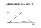
図6は、バッテリ51の時間経過における充電電圧と充電電流の特性の一例を示す図である。縦軸が電圧又は電流を表し、横軸が時間を表す。縦軸と横軸の単位は、任意である。情報処理装置200の電源状態がオフ状態である場合にACアダプタ100からバッテリ51に充電するとき、ACアダプタ100の過電流保護特性は逆L字特性であるから、ACアダプタ100の定格出力電流の定格電流値I7で定電流充電が始まる。つまり、定格電流値I7は、図2の定格電流値I1に等しい。
FIG. 6 is a diagram illustrating an example of the characteristics of the charging voltage and the charging current over time of the
図6において、放電終止電圧V5から充電上限電圧V6(設定値)まで充電量に応じて時間経過と共にバッテリ電圧Vbattが上昇する。バッテリ電圧Vbattが充電上限電圧V6に達したことがコンパレータCP1により検出されると、電源制御回路52は、充電回路50を迂回する経路から、充電回路50を経由する経路に切り替える。
In FIG. 6, the battery voltage Vbatt rises with time from the discharge end voltage V5 to the charge upper limit voltage V6 (set value) according to the amount of charge. When the comparator CP1 detects that the battery voltage Vbatt has reached the charging upper limit voltage V6, the power
充電回路50を経由する経路に切り替わることにより、充電回路50は、充電上限電圧V6を定電圧値とする定電圧制御で、バッテリ51を定電圧充電する。バッテリ51が定電圧充電されることにより、バッテリ51の充電電流の電流値は電流値I8まで絞られて低くなる。
By switching to a path that passes through the charging
以上、情報処理装置、電源制御回路及びACアダプタを実施形態により説明したが、本発明は上記実施形態に限定されるものではない。他の実施形態の一部又は全部との組み合わせや置換などの種々の変形及び改良が、本発明の範囲内で可能である。 As described above, the information processing apparatus, the power supply control circuit, and the AC adapter have been described according to the embodiments. However, the present invention is not limited to the above embodiments. Various modifications and improvements such as combinations and substitutions with some or all of the other embodiments are possible within the scope of the present invention.
例えば、情報処理装置は、可搬型でもよいし、定置型でもよい。また、情報処理装置は、パーソナルコンピュータ以外のバッテリ駆動可能な電子機器(例えば、携帯電話等の移動無線端末、スマートフォンなど)でもよい。 For example, the information processing apparatus may be portable or stationary. The information processing apparatus may be a battery-driven electronic device other than a personal computer (for example, a mobile wireless terminal such as a mobile phone, a smartphone, or the like).
また、例えば、使用されるトランジスタは、MOSトランジスタに限らず、バイポーラトランジスタなどの他のスイッチング素子が使用されてよい。 For example, the transistor used is not limited to a MOS transistor, and other switching elements such as a bipolar transistor may be used.
以上の実施形態に関し、更に以下の付記を開示する。
(付記1)
ACアダプタから出力されるDC出力によって充電されるバッテリを備える情報処理装置であって、
前記情報処理装置の電源状態に応じて前記ACアダプタの過電流保護特性を切り替える電源制御回路を備え、
前記電源制御回路は、前記電源状態がオフからオンに変化すると、前記過電流保護特性を逆L字特性からフの字特性に切り替える、ことを特徴とする、情報処理装置。
(付記2)
前記フの字特性のピーク電流値は、前記逆L字特性の定電流値よりも大きい、付記1に記載の情報処理装置。
(付記3)
前記DC出力に基づいて前記バッテリを定電圧で充電する充電回路を備え、
前記電源制御回路は、前記電源状態がオフからオンに変化すると、前記バッテリの充電経路を前記充電回路を経由する回路経路に切り替える、付記1又は2に記載の情報処理装置。
(付記4)
前記電源制御回路は、前記電源状態がオンからオフに変化すると、前記充電経路を前記充電回路を迂回する迂回経路に切り替える、付記3に記載の情報処理装置。
(付記5)
前記電源制御回路は、前記充電経路が前記迂回経路である場合に前記バッテリのバッテリ電圧が設定値に達すると、前記充電経路を前記回路経路に切り替える、付記4に記載の情報処理装置。
(付記6)
ACアダプタから出力されるDC出力によって充電されるバッテリを備える情報処理装置の電源状態を検出する検出部と、
前記検出部により検出された電源状態に応じて前記ACアダプタの過電流保護特性を切り替える制御信号を送信する送信部とを備え、
前記送信部は、前記電源状態がオフからオンに変化すると、前記過電流保護特性を逆L字特性からフの字特性に切り替える制御信号を送信する、ことを特徴とする、電源制御回路。
(付記7)
前記フの字特性のピーク電流値は、前記逆L字特性の定電流値よりも大きい、付記6に記載の電源制御回路。
(付記8)
前記電源状態がオフからオンに変化すると、前記バッテリの充電経路を、前記DC出力に基づいて前記バッテリを定電圧で充電する充電回路を経由する回路経路に切り替える、付記6又は7に記載の電源制御回路。
(付記9)
前記電源状態がオンからオフに変化すると、前記充電経路を前記充電回路を迂回する迂回経路に切り替える、付記8に記載の電源制御回路。
(付記10)
前記充電経路が前記迂回経路である場合に前記バッテリのバッテリ電圧が設定値に達すると、前記充電経路を前記回路経路に切り替える、付記9に記載の電源制御回路。
(付記11)
情報処理装置のバッテリを充電するDC出力を出力する出力回路と、
前記情報処理装置の電源状態を前記情報処理装置から受信して、前記出力回路の過電流保護特性を切り替える切り替え回路とを備え、
前記切り替え回路は、前記電源状態がオフからオンに変化すると、前記過電流保護特性を逆L字特性からフの字特性に切り替える、ことを特徴とする、ACアダプタ。
(付記12)
前記フの字特性のピーク電流値は、前記逆L字特性の定電流値よりも大きい、付記11に記載のACアダプタ。
Regarding the above embodiment, the following additional notes are disclosed.
(Appendix 1)
An information processing apparatus including a battery charged by a DC output output from an AC adapter,
A power supply control circuit that switches overcurrent protection characteristics of the AC adapter according to the power supply state of the information processing apparatus;
The information processing apparatus according to
(Appendix 2)
The information processing apparatus according to
(Appendix 3)
A charging circuit for charging the battery at a constant voltage based on the DC output;
The information processing apparatus according to
(Appendix 4)
The information processing apparatus according to appendix 3, wherein the power supply control circuit switches the charging path to a bypass path that bypasses the charging circuit when the power state changes from on to off.
(Appendix 5)
The information processing apparatus according to appendix 4, wherein the power supply control circuit switches the charging path to the circuit path when the battery voltage of the battery reaches a set value when the charging path is the bypass path.
(Appendix 6)
A detection unit for detecting a power state of an information processing apparatus including a battery charged by a DC output output from an AC adapter;
A transmission unit that transmits a control signal for switching overcurrent protection characteristics of the AC adapter according to the power supply state detected by the detection unit;
The power transmission control circuit, wherein the transmission unit transmits a control signal for switching the overcurrent protection characteristic from an inverted L-characteristic to a F-characteristic when the power supply state changes from off to on.
(Appendix 7)
The power supply control circuit according to appendix 6, wherein a peak current value of the U-shaped characteristic is larger than a constant current value of the inverted L-shaped characteristic.
(Appendix 8)
The power supply according to appendix 6 or 7, wherein when the power state changes from off to on, the charging path of the battery is switched to a circuit path via a charging circuit that charges the battery with a constant voltage based on the DC output. Control circuit.
(Appendix 9)
The power supply control circuit according to appendix 8, wherein when the power state changes from on to off, the charging path is switched to a bypass path that bypasses the charging circuit.
(Appendix 10)
The power supply control circuit according to appendix 9, wherein when the battery path of the battery reaches a set value when the charging path is the bypass path, the charging path is switched to the circuit path.
(Appendix 11)
An output circuit for outputting a DC output for charging the battery of the information processing apparatus;
A switching circuit that receives a power state of the information processing device from the information processing device and switches overcurrent protection characteristics of the output circuit;
The AC adapter, wherein the switching circuit switches the overcurrent protection characteristic from an inverted L-characteristic to a F-characteristic when the power supply state changes from off to on.
(Appendix 12)
The AC adapter according to
30 フの字特性回路
40 逆L字特性回路
50 充電回路
51 バッテリ
52 電源制御回路
53 検出部
54 送信部
60 出力回路
70 切り替え回路
100 ACアダプタ
200 情報処理装置
30 Characteristic Characteristic Circuit 40 Reverse L
Claims (7)
前記DC出力に基づいて前記バッテリを定電圧で充電する充電回路と、
前記情報処理装置の電源状態がオフからオンに変化すると、前記ACアダプタの過電流保護特性を逆L字特性からフの字特性に切り替える電源制御回路とを備え、
前記電源制御回路は、前記電源状態がオフからオンに変化すると、前記バッテリの充電経路を前記充電回路を経由する回路経路に切り替え、前記電源状態がオンからオフに変化すると、前記充電経路を前記充電回路を迂回する迂回経路に切り替え、前記充電経路が前記迂回経路である場合に前記バッテリのバッテリ電圧が設定値に達すると、前記充電経路を前記回路経路に切り替える、情報処理装置。 An information processing apparatus including a battery charged by a DC output output from an AC adapter,
A charging circuit for charging the battery at a constant voltage based on the DC output;
Wherein the power supply state of the information processing apparatus is changed from OFF to ON, and a power supply control circuit for switching the overcurrent protection characteristics inverted L-shape characteristics from the off-characteristic of the AC adapter,
The power control circuit switches the charging path of the battery to a circuit path via the charging circuit when the power state changes from off to on, and changes the charging path when the power state changes from on to off. An information processing apparatus that switches to a bypass path that bypasses a charging circuit, and switches the charging path to the circuit path when the battery voltage of the battery reaches a set value when the charging path is the bypass path .
前記検出部により検出された電源状態がオフからオンに変化すると、前記ACアダプタの過電流保護特性を逆L字特性からフの字特性に切り替える制御信号を送信する送信部とを備え、
前記送信部は、前記電源状態がオフからオンに変化すると、前記バッテリの充電経路を、前記DC出力に基づいて前記バッテリを定電圧で充電する充電回路を経由する回路経路に切り替える信号を送信し、前記電源状態がオンからオフに変化すると、前記充電経路を前記充電回路を迂回する迂回経路に切り替える信号を送信し、前記充電経路が前記迂回経路である場合に前記バッテリのバッテリ電圧が設定値に達すると、前記充電経路を前記回路経路に切り替える信号を送信する、電源制御回路。 A detection unit for detecting a power state of an information processing apparatus including a battery charged by a DC output output from an AC adapter;
A transmission unit for transmitting a control signal for switching the overcurrent protection characteristic of the AC adapter from the inverted L-shaped characteristic to the F-shaped characteristic when the power supply state detected by the detecting unit changes from off to on ;
When the power state changes from off to on, the transmission unit transmits a signal for switching the charging path of the battery to a circuit path via a charging circuit that charges the battery with a constant voltage based on the DC output. When the power state changes from on to off, a signal for switching the charging path to a bypass path that bypasses the charging circuit is transmitted, and when the charging path is the bypass path, the battery voltage of the battery is set to a set value A power supply control circuit that transmits a signal for switching the charging path to the circuit path when reaching .
前記情報処理装置の電源状態を前記情報処理装置から受信して、前記出力回路の過電流保護特性を切り替える切り替え回路とを備え、
前記情報処理装置は、前記DC出力に基づいて前記バッテリを定電圧で充電する充電回路と、前記電源状態がオフからオンに変化すると、前記バッテリの充電経路を前記充電回路を経由する回路経路に切り替え、前記電源状態がオンからオフに変化すると、前記充電経路を前記充電回路を迂回する迂回経路に切り替え、前記充電経路が前記迂回経路である場合に前記バッテリのバッテリ電圧が設定値に達すると、前記充電経路を前記回路経路に切り替える電源制御回路とを有し、
前記切り替え回路は、前記情報処理装置から受信した前記電源状態がオフからオンに変化すると、前記過電流保護特性を逆L字特性からフの字特性に切り替える、ことを特徴とする、ACアダプタ。 An output circuit for outputting a DC output for charging the battery of the information processing apparatus;
A switching circuit that receives a power state of the information processing device from the information processing device and switches overcurrent protection characteristics of the output circuit;
The information processing apparatus includes: a charging circuit that charges the battery with a constant voltage based on the DC output; and when the power supply state changes from off to on, the charging path of the battery is changed to a circuit path that passes through the charging circuit. When the power supply state changes from on to off, the charging path is switched to a bypass path that bypasses the charging circuit, and when the battery voltage of the battery reaches a set value when the charging path is the bypass path A power supply control circuit for switching the charging path to the circuit path,
The AC adapter, wherein the switching circuit switches the overcurrent protection characteristic from an inverted L-characteristic to a F-characteristic when the power supply state received from the information processing apparatus changes from off to on.
Priority Applications (1)
| Application Number | Priority Date | Filing Date | Title |
|---|---|---|---|
| JP2014006068A JP6201775B2 (en) | 2014-01-16 | 2014-01-16 | Information processing apparatus, power supply control circuit, and AC adapter |
Applications Claiming Priority (1)
| Application Number | Priority Date | Filing Date | Title |
|---|---|---|---|
| JP2014006068A JP6201775B2 (en) | 2014-01-16 | 2014-01-16 | Information processing apparatus, power supply control circuit, and AC adapter |
Publications (2)
| Publication Number | Publication Date |
|---|---|
| JP2015135564A JP2015135564A (en) | 2015-07-27 |
| JP6201775B2 true JP6201775B2 (en) | 2017-09-27 |
Family
ID=53767360
Family Applications (1)
| Application Number | Title | Priority Date | Filing Date |
|---|---|---|---|
| JP2014006068A Active JP6201775B2 (en) | 2014-01-16 | 2014-01-16 | Information processing apparatus, power supply control circuit, and AC adapter |
Country Status (1)
| Country | Link |
|---|---|
| JP (1) | JP6201775B2 (en) |
Families Citing this family (1)
| Publication number | Priority date | Publication date | Assignee | Title |
|---|---|---|---|---|
| JP6144809B1 (en) * | 2016-09-05 | 2017-06-07 | ホシデン株式会社 | Power supply |
Family Cites Families (6)
| Publication number | Priority date | Publication date | Assignee | Title |
|---|---|---|---|---|
| JPS6140623A (en) * | 1984-07-31 | 1986-02-26 | Toko Inc | Dc power supply device |
| JPH0795247B2 (en) * | 1986-09-22 | 1995-10-11 | 日立照明株式会社 | DC power supply |
| JPS63124731A (en) * | 1986-11-14 | 1988-05-28 | 株式会社東芝 | Charger of secondary battery in electronic equipment |
| JPH0340728A (en) * | 1989-07-05 | 1991-02-21 | Nec Corp | Portable radio telephone charger |
| JP2604275B2 (en) * | 1990-11-14 | 1997-04-30 | 三洋電機株式会社 | Electronic device charge control method |
| JP2914259B2 (en) * | 1995-12-14 | 1999-06-28 | 日本電気株式会社 | Portable electronic device and charge control method for portable electronic device |
-
2014
- 2014-01-16 JP JP2014006068A patent/JP6201775B2/en active Active
Also Published As
| Publication number | Publication date |
|---|---|
| JP2015135564A (en) | 2015-07-27 |
Similar Documents
| Publication | Publication Date | Title |
|---|---|---|
| US9859737B2 (en) | Method and apparatus for performing system power management in electronic device equipped with battery | |
| US9715244B2 (en) | System and method for determining adapter current limit | |
| US7522432B2 (en) | Switching regulator and control circuit and method used therein | |
| US9231419B2 (en) | Semiconductor device and battery pack | |
| US9430008B2 (en) | Apparatus and method for optimizing use of NVDC chargers | |
| US8947060B2 (en) | Regulator over-voltage protection circuit with reduced standby current | |
| KR101769130B1 (en) | Power supply, apparatus and method for controlling link voltage control switch | |
| JP2016504907A (en) | Electric circuit for supplying power to home appliances | |
| KR101877371B1 (en) | Apparatus and method for protecting supply modulator | |
| US9472967B2 (en) | Power management system and method for a portable device | |
| US20140184154A1 (en) | Electronic component, power receiving device, and power feeding system | |
| JP2008187813A (en) | Switching power supply | |
| US11387676B2 (en) | Dual-mode high-efficiency voltage regulator for wireless charging modules | |
| JP5811246B1 (en) | DC-DC converter | |
| JP2012196109A (en) | Control circuit of switching power supply device, and switching power supply device | |
| US10396674B2 (en) | Flyback power converter circuit and primary side controller circuit thereof | |
| CN212486401U (en) | Power supply and peripheral circuit for power supply | |
| US8830706B2 (en) | Soft-start circuit | |
| JP2017200386A (en) | Dc-dc converter | |
| JP2007189771A (en) | Power unit | |
| JP6201775B2 (en) | Information processing apparatus, power supply control circuit, and AC adapter | |
| KR102195589B1 (en) | Charging control apparatus, charging system, and charging control method | |
| CN109217677B (en) | Flyback power supply circuit and primary side control circuit thereof | |
| US9048661B2 (en) | Battery protection circuits | |
| US20210057987A1 (en) | High Voltage Start-up Circuit for Switching Power Supplies |
Legal Events
| Date | Code | Title | Description |
|---|---|---|---|
| A621 | Written request for application examination |
Free format text: JAPANESE INTERMEDIATE CODE: A621 Effective date: 20160905 |
|
| A977 | Report on retrieval |
Free format text: JAPANESE INTERMEDIATE CODE: A971007 Effective date: 20170419 |
|
| A131 | Notification of reasons for refusal |
Free format text: JAPANESE INTERMEDIATE CODE: A131 Effective date: 20170425 |
|
| A521 | Request for written amendment filed |
Free format text: JAPANESE INTERMEDIATE CODE: A523 Effective date: 20170612 |
|
| TRDD | Decision of grant or rejection written | ||
| A01 | Written decision to grant a patent or to grant a registration (utility model) |
Free format text: JAPANESE INTERMEDIATE CODE: A01 Effective date: 20170801 |
|
| A61 | First payment of annual fees (during grant procedure) |
Free format text: JAPANESE INTERMEDIATE CODE: A61 Effective date: 20170814 |
|
| R150 | Certificate of patent or registration of utility model |
Ref document number: 6201775 Country of ref document: JP Free format text: JAPANESE INTERMEDIATE CODE: R150 |
|
| S111 | Request for change of ownership or part of ownership |
Free format text: JAPANESE INTERMEDIATE CODE: R313113 |
|
| R350 | Written notification of registration of transfer |
Free format text: JAPANESE INTERMEDIATE CODE: R350 |
|
| R250 | Receipt of annual fees |
Free format text: JAPANESE INTERMEDIATE CODE: R250 |
|
| R250 | Receipt of annual fees |
Free format text: JAPANESE INTERMEDIATE CODE: R250 |