JP6199012B2 - Game machine - Google Patents
Game machine Download PDFInfo
- Publication number
- JP6199012B2 JP6199012B2 JP2012137837A JP2012137837A JP6199012B2 JP 6199012 B2 JP6199012 B2 JP 6199012B2 JP 2012137837 A JP2012137837 A JP 2012137837A JP 2012137837 A JP2012137837 A JP 2012137837A JP 6199012 B2 JP6199012 B2 JP 6199012B2
- Authority
- JP
- Japan
- Prior art keywords
- value
- rotation
- stop
- rotating
- signal
- Prior art date
- Legal status (The legal status is an assumption and is not a legal conclusion. Google has not performed a legal analysis and makes no representation as to the accuracy of the status listed.)
- Active
Links
Images


Description
本発明は、コンピュータ装置を内蔵する電子遊技機に関し、特に、回胴遊技機に好適に適用される。 The present invention relates to an electronic game machine with a built-in computer device, and is particularly preferably applied to a spinning game machine.
スロットマシンなどの回胴遊技機では、遊技者がメダル投入口にメダルを投入してスタートレバーを操作すると、これに応じて、回転リールの回転が開始される。そして、遊技者がストップボタンを押して回転リールを停止させたとき、有効な停止ライン(以下、有効ラインという)に図柄が揃うと、その図柄に応じた配当メダルが払い出されるようになっている。 In a spinning machine such as a slot machine, when a player inserts a medal into a medal slot and operates a start lever, the rotation of the rotating reel is started accordingly. When the player presses the stop button to stop the rotating reel, when the symbols are aligned on an effective stop line (hereinafter referred to as an effective line), a payout medal corresponding to the symbol is paid out.
但し、実際には、各ゲームの当否状態は、遊技者が停止操作を開始するまでに、主制御部における内部抽選処理(以下、図柄抽選処理ということがある)によって予め決定されており、この抽選処理によって内部当選した図柄を、遊技者が有効ライン上に揃えることで配当メダルが払出される(特許文献1〜特許文献3)。
However, in reality, the success / failure state of each game is determined in advance by an internal lottery process (hereinafter also referred to as a symbol lottery process) in the main control unit before the player starts the stop operation. A payout medal is paid out when the player arranges the symbols that are won internally by the lottery process on the active line (
このような動作を実現する制御動作のうち、特に問題になるのは、制御時間に余裕がなく、且つ、誤動作が許されない停止制御である。すなわち、ストップボタンのON操作から所定の回転角度の範囲内で、内部抽選処理の当選結果に対応する図柄を停止させる必要があるので、迅速な処理が要求される一方、ストップボタン操作を誤認して不自然な停止制御を実行したのでは遊技者に大きな不信感を与えてしまう。 Among the control operations that realize such an operation, the problem that is particularly problematic is stop control that does not allow a control time and does not allow malfunction. In other words, since it is necessary to stop the symbol corresponding to the winning result of the internal lottery process within the range of the predetermined rotation angle from the ON operation of the stop button, while prompt processing is required, the stop button operation is mistakenly recognized. If unnatural stop control is executed, the player will be greatly distrusted.
本発明は、上記の問題点に鑑みてなされたものであって、スイッチ信号の目的に応じた適切な制御動作を実現できる遊技機を提供することを目的とする。 The present invention has been made in view of the above problems, and an object of the present invention is to provide a gaming machine capable of realizing an appropriate control operation according to the purpose of a switch signal.
上記の目的を達成するため、本発明は、遊技者の遊技操作に対応して遊技動作を進行させるメイン処理と、所定時間毎に前記メイン処理を中断させて実行される割込み処理と、を有し、遊技操作として、複数の回転体を停止させる停止操作が許容される遊技機であって、プログラム処理によって書換え可能な管理情報を、前記メイン処理と前記割込み処理が適宜に設定又は参照することで、停止操作を受けた回転体が所定の抽選処理の抽選結果に基づく態様で停止可能に構成され、前記メイン処理は、遊技者による遊技開始の遊技操作を認識した後、正方向の起動回転から定常回転に至る回転体の正常回転を開始させるべく、管理情報を第1値に設定する第1手段と、管理情報が第2値であることを条件に、定常回転中の回転体に対する停止操作の有効性を判定し、有効な停止操作と認識すると、前記抽選結果に基づいて停止位置を決定し、適宜なタイミングで、管理情報を第3値に設定する第2手段と、を有して構成され、前記割込み処理は、管理情報が第1値に設定されたことに基づいて、回転体の回転速度を漸次加速させる起動回転の後、回転体を定常回転させると共に、回転体が基準位置を通過すると、管理情報を第2値に設定する第3手段と、第3手段による回転体の定常回転の後、前記メイン処理によって、管理情報が第3値に設定されたことに基づいて、所定位置で回転体を停止させ、その後の所定時間、同一の励磁状態を維持する第4手段と、を有して構成され、前記メイン処理の第2手段は、停止操作の有効性の判定において、停止状態又は停止制御を開始した回転体に対する停止操作を無視するよう構成されている。 In order to achieve the above object, the present invention includes a main process for proceeding with a game operation in response to a player's game operation, and an interrupt process executed by interrupting the main process at predetermined intervals. and, as a game operation, a game machine stop operation for stopping the plurality of rotating bodies is allowed, the management information can be rewritten by the program processing, that the interrupt processing and the main processing is set or reference to appropriate Thus, the rotating body that has received the stop operation is configured to be able to stop in a manner based on a lottery result of a predetermined lottery process, and the main process recognizes the game operation of the game start by the player and then starts the rotation in the forward direction. in order to start the normal rotation of the rotating body reaches the normal rotation from a first means for setting the management information to the first value, on condition that the management information is the second value, stop for the rotating body in the steady-state rotation To determine the effectiveness of work, effective stop operation and the recognition result to determine the stop position based on the lottery result, at an appropriate timing, and a second means for setting the management information to the third value, the The interrupt process is configured such that, based on the fact that the management information is set to the first value, after the start-up rotation for gradually accelerating the rotation speed of the rotating body, the rotating body is rotated in a steady state , and the rotating body is set as a reference. After passing the position, based on the third means for setting the management information to the second value, and after the steady rotation of the rotating body by the third means , the management information is set to the third value by the main processing. And a fourth means for stopping the rotating body at a predetermined position and maintaining the same excitation state for a predetermined time thereafter, and the second means of the main processing is for determining the effectiveness of the stop operation. In stop state or stop control started It is configured to ignore the stop operation for rotating body.
上記した本発明に係る遊技機によれば、メイン処理と割込み処理が適宜に協働することで、停止制御動作を適切に実現することができる。 According to the gaming machine according to the present invention described above , the stop control operation can be appropriately realized by appropriately cooperating the main process and the interrupt process .
以下、実施例に基づいて本発明を更に詳細に説明する。図1〜図4は、実施例に係るスロットマシンSLを図示したものである。本スロットマシンSLは、矩形箱状の本体ケース1と、各種の遊技部材を装着した前面パネル2とが、ヒンジ3を介して連結され、前面パネル2が本体ケース1に対して開閉可能に構成されている(図2)。そして、図1は前面パネル2の正面図、図2はスロットマシンSLの右側面図(a)と平面図(b)、図3は前面パネル2の背面図、図4は本体ケース1の内部正面図を示している。
Hereinafter, the present invention will be described in more detail based on examples. 1 to 4 illustrate a slot machine SL according to an embodiment. In this slot machine SL, a rectangular box-shaped
図4に示す通り、本体ケース1の略中央には、3つの回転リール4a〜4cを備える図柄回転ユニット4が配置され、その下側に、メダル払出装置5が配置されている。各回転リール4a〜4cには、BB図柄、RB図柄、各種のフルーツ図柄、及びリプレイ図柄などが描かれている。メダル払出装置5には、メダルを貯留するメダルホッパー5aと、払出モータMと、メダル払出制御基板55と、払出中継基板63と、払出センサ(不図示)などが設けられている。ここで、メダルは、払出モータMの回転に基づいて、払出口5bから図面手前に向けて導出される。なお、限界量を越えて貯留されたメダルは、オーバーフロー部5cを通して、補助タンク6に落下するよう構成されている。
As shown in FIG. 4, a
上記のメダル払出装置5に隣接して電源基板62が配置され、また、図柄回転ユニット4の上部に主制御基板50が配置され、主制御基板50に隣接して回胴設定基板54が配置されている。なお、図柄回転ユニット4の内部には、回胴LED中継基板58と回胴中継基板57とが設けられ、図柄回転ユニット4に隣接して外部集中端子板56が配置されている。
A
図1に示すように、前面パネル2の上部には液晶表示ユニット7が配置されている。この表示ユニット7には、各種のキャラクタを表示することで遊技動作を効果的に盛り上げている。液晶表示ユニット7の下部には、回転リール4a〜4cに対応する3つの表示窓8a〜8cが配置されている。表示窓8a〜8cを通して、各回転リール4a〜4cの回転方向に、各々3個程度の図柄が見えるようになっており、合計9個の図柄の水平方向の三本と、対角線方向の二本が仮想的な停止ラインとなる。
As shown in FIG. 1, a liquid
このような表示窓8aの左側には、遊技状態を示すLED群9が設けられ、その下方には、遊技成果として払出されるメダル数を表示する払出表示部10や、クレジット状態のメダル数を表示する貯留数表示部11が設けられている。
On the left side of the
払出表示部10は、7セグメントLEDを2個連設して構成されており、払出メダル数を特定すると共に、何らかの異常事態の発生時には、異常内容を表示するエラー表示器としても機能している。
The
前面パネル2の垂直方向中央には、メダルを投入するメダル投入口12が設けられ、これに隣接して、メダル投入口12に詰まったメダルを返却させるための返却ボタン13が設けられている。また、クレジット状態のメダルを払出すクレジット精算ボタン14と、メダル投入口12へのメダル投入に代えてクレジット状態のメダルを擬似的に一枚投入する投入ボタン15と、クレジット状態のメダルを擬似的に三枚投入するマックス投入ボタン16とが設けられている。
In the center of the
これらの遊技部材の下方には、回転リール4a〜4cの回転を開始させるスタートレバー17と、回転中の回転リール4a〜4cを停止させるためのストップボタン18a〜18cが設けられている。
Below these game members, a
遊技者がスタートレバー17を操作すると、通常は、3つの回転リール4a〜4cが、正方向に正常回転を開始するが、内部当選状態を予告するリール演出時には、回転リール4a〜4cの全部又は一部が、変則的に回転した上で正常回転を開始する。
When the player operates the
図1に示す通り、前面パネル2の下方には、メダルを蓄える横長の受け皿19と、払出装置5の払出口5bに連通するメダル導出口20とが設けられている。なお、メダル導出口20の左右にはスピーカSPが配置されている。
As shown in FIG. 1, a horizontally
図3に示すように、前面パネル2の裏側には、メダル投入口12に投入されたメダルの選別を行うメダル選別装置21と、メダル選別装置21により不適正と判別されたメダルをメダル導出口20に案内する返却通路22とが設けられている。また、前面パネル3の裏側上部には、演出制御基板51、演出インタフェイス基板52、及び液晶制御基板61などを収容する基板ケース23が配置されている。そして、メダル選別装置21の上部には、図1に示す各種の遊技部材と主制御基板50との間の信号を中継する遊技中継基板53が設けられている。
As shown in FIG. 3, on the back side of the
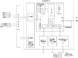
図5は、実施例に係るスロットマシンSLの回路構成を示すブロック図である。図示の通り、このスロットマシンSLは、回転リール4a〜4cを含む各種の遊技部材の動作を制御する主制御基板50と、主制御基板50から受けた制御コマンドに基づいて演出動作を実現する演出制御基板51と、交流電圧(24V)を直流電圧(5V,12V,24V)に変換して装置各部に供給する電源基板62とを中心に構成されている。
FIG. 5 is a block diagram illustrating a circuit configuration of the slot machine SL according to the embodiment. As shown in the figure, this slot machine SL realizes an effect operation based on a
主制御基板50は、演出制御基板51に対して、スピーカSPによる音声演出、LEDランプや冷陰極線管放電管によるランプ演出、及び、液晶表示ユニット7による図柄演出を実現するための制御コマンドを出力している。そして、演出制御部51では、主制御基板50から、内部抽選結果を特定する制御コマンド(遊技開始コマンド)受けると、内部抽選結果に対応してアシストタイム当選状態とするか否かのAT抽選を実行している。
The
また、演出制御部51は、主制御基板50から、リール演出を実行することを示す制御コマンド(フリーズコマンド)を受けた場合には、主制御基板50で実行するリール演出に対応する適宜な演出動作を開始する。
In addition, when receiving a control command (freeze command) indicating that the reel effect is to be executed from the
これらの動作のため、演出制御基板51は、演出インタフェイス基板52を通して、液晶制御基板61に接続されており、液晶制御基板61は、液晶表示(LCD)ユニット7における適宜な図柄演出を実現している。
For these operations, the
また、演出制御基板51は、演出インタフェイス基板52と共に、LED基板59やインバータ基板60や回胴LEDドライブ基板58を経由して、各種のLEDや冷陰極線管放電管におけるランプ演出を実現している。更にまた、演出制御基板51は、演出インタフェイス基板52を通してスピーカSPを駆動して音声演出を実現している。
The
なお、演出制御基板51においてAT抽選に当選した後の所定回数のゲーム(AT中)では、小役当選状態において、その図柄を停止ラインに整列できるよう、3つの回転リールの停止順序を遊技者に報知している。
In addition, in a predetermined number of games (during AT) after winning the AT lottery on the
主制御基板50は、遊技中継基板53を通して、スロットマシンの各種遊技部材に接続されている。具体的には、スタートレバー17の始動スイッチ、ストップボタン18a〜18cの停止スイッチ、投入ボタン15,16の投入スイッチ、清算ボタン14の清算スイッチ、前面パネル2の開閉を認識するドアセンサ、上流側センサを構成するレバー検知センサ、メダル通過センサを構成するフォトインタラプタPH1,PH2、不正メダルの通過を阻止するブロッカーをON/OFF制御するブロッカーソレノイド30、及び、各種LED素子9〜11などに接続されている。
The
このように、主制御基板50は、遊技中継基板53を経由して、各種のスイッチ信号を受けるが、スタートレバー17の操作を示すスタートレバー信号LVについては、I/Oポート回路64eと、乱数生成回路GNRに重複して供給されている(図7参照)。そして、乱数生成回路GNRでは、スタートレバー信号LVのONエッジに基づいてハード乱数値を生成している。また、I/Oポート回路64eを経由して受けるスタートレバー信号LVに基づいて、回転リールの回転開始に向けた動作を開始させている。なお、この実施例では、便宜上、スタートレバー信号LVのOFFエッジに基づいて回転リールの回転開始に向けた処理を開始するが、ONエッジに基づいて処理を開始させるのも好適である。
As described above, the
図5に示す通り、主制御基板50は、回胴中継基板57を経由して、回転リール4a〜4cを回転させる3つのステッピングモータ、及び、回転リール4a〜4cの基準位置を検出するためのインデックスセンサに接続されている。そして、ステッピングモータを駆動又は停止させることによって、回転リール4a〜4cの回転動作と、目的位置での停止動作を実現している。
As shown in FIG. 5, the
また、主制御基板50は、払出中継基板63を通してメダル払出装置5にも接続されている。メダル払出装置5には、メダル払出制御基板55と、メダル満杯センサと、メダル払出センサと、払出モータMとが設けられており、メダル払出制御基板55は、主制御基板50からの制御コマンドに基づいて払出モータMを回転させて、所定量のメダルを払出している。
The
メダル満杯センサは、補助収納庫にメダルが満杯状態になったオーバーフロー異常を検出し、メダル払出センサは、払出メダル枚数が不足する不足異常や、遊技機による払出動作を伴わない異常払出を検出している。そして、これらのセンサ信号は、ドア開放センサなどと共に、払出中継基板63を経由して主制御基板50に伝送される(図5、図7参照)。
The medal full sensor detects an overflow error when the auxiliary storage is full of medals, and the medal payout sensor detects a shortage error that the number of payout medals is insufficient or an abnormal payout that is not accompanied by a payout operation by a gaming machine. ing. These sensor signals are transmitted to the
その他、主制御基板50は、外部集中端子板56と、回胴設定基板54にも接続されている。外部集中端子板56は、例えばホールコンピュータHCに接続されており、主制御基板50は、外部集中端子板56を通して、メダルの投入枚数やメダルの払出枚数などを出力している。
In addition, the
また、回胴設定基板54は、遊技機の設定値を変更するために、係員が該当キー穴に設定キーを挿入したこと示す設定キー信号などを出力している。ここで、設定値とは、当該遊技機で実行される抽選処理の当選確率などを、設定1から設定6まで6段階で規定するもので、遊技ホールの営業戦略に基づいて適宜に設定される。例えば、最高ランクに設定された遊技機は、メダル払出枚数の期待値が最高レベルであるため、遊技者にとって最も有利である。
Further, the rotating
そして、設定キー信号は、リセットスイッチ信号、自動清算スイッチ信号、打ち止めスイッチ信号などと共に、回胴設定基板54から主制御基板50に伝送されている(図5、図7参照)。なお、リセットスイッチは、係員によって操作され、設定キー挿入時には、設定値の変更を主制御部50に指示するために使用され、異常時には、その異常事態が解消されたことを主制御部50に通知するために使用される。
The setting key signal is transmitted from the rotating
図6は、電源基板62の回路構成を示すブロック図である。この電源基板62は、交流24Vを受けて脈流電圧に変換する整流部80と、脈流電圧を直流5Vに変換する第1電圧変換部81と、脈流電圧を直流12Vに変換する第2電圧変換部82と、脈流電圧を直流24Vに変換する第3電圧変換部83と、第1電圧変換部81の出力電圧を蓄電する蓄電部84と、電源投入を検出して電源リセット信号RSTを出力すると共に、電源電圧の降下を検出して電源異常ABNを出力する電源監視部85とで構成されている。
FIG. 6 is a block diagram showing a circuit configuration of the
蓄電部84は、大容量(1ファラッド程度)のコンデンサCと、過電流用の制限抵抗r1、r2と、逆方向電流を阻止するダイオードDとで構成されている。なお、制限抵抗r1は75Ω程度、制限抵抗r2は10Ω程度である。コンデンサCの両端電圧は、バックアップ電源として、ワンチップマイコン64に供給されている。
The
このバックアップ電源は、ワンチップマイコン64に内蔵されたSRAM(static ram)に供給されており、電源電圧の遮断状態でも、通常7〜8日はRAM(Random Access Memory)の記憶内容を保持するようにしている。なお、RAMの記憶容量は、この実施例では、遊技機のワークエリアとして使用される512バイト程度である。
This backup power is supplied to an SRAM (static ram) built in the one-
電源監視部85は、交流入力電圧24Vの電圧レベルと、直流電源電圧5Vの電圧レベルとを監視している。そして、何れか一方のレベルが所定値を下回ると、電源異常信号ABNが異常レベルに変化するよう構成されている。瞬停や停電などの異常時には、先ず、交流入力電圧の電圧降下に対応して、電源異常信号ABNが素早く出力される。
The power
図7は、主制御基板50の回路構成を図示したものである。図示の通り、主制御基板50は、ワンチップマイコン64と、回胴モータ駆動回路65と、演出制御基板51やその他の基板53,54,56,63とのインタフェイス基板66〜68とを中心に構成されている。インタフェイス回路66は、演出制御基板51に制御コマンドを出力するための8ビットパラレルポートである。また、回胴モータ駆動回路69は、回転リール4a〜4cのステッピングモータの駆動信号を生成する回路であり、回胴中継基板57を経由して回転リールを回転駆動及び停止駆動を実現している。
FIG. 7 illustrates the circuit configuration of the
ワンチップマイコン64は、Z80相当品のCPUコア64a、ROM、RAMの他に、CTC(Counter/Timer Circuit) 64b、割込みコントローラ64c、I/Oポート回路64d,64e、及び、乱数生成回路GNRを内蔵している。なお、I/Oポート回路は、後述する入力ポートIN0〜入力ポートIN2を含んでいる。
The one-
図示の通り、ワンチップマイコン64のリセット端子RSTには、電源基板62から受ける電源リセット信号RSTが供給されている。そのため、電源投入時には、CPUコア64aがリセット状態となり、ROMの先頭アドレス以降の制御プログラム(図10)の実行が開始される。
As shown in the figure, a power reset signal RST received from the
また、ワンチップマイコン64の割込み端子NMI(Non Maskable Interrupt)には、電源基板62から受ける電源異常信号ABNが供給されている。そのため、電源異常時には、CPUコア64aが割込み許可状態であるか否かに拘らず、NMI割込み処理(図13(b))が起動される。図示の通り、電源異常信号ABNは、割込み端子NMIに供給される一方、I/Oポート回路64eにも供給されている。ここで、割込み端子NMIに供給される電源異常信号ABNは、2つのNOTゲートを経由することで所定の遅延時間が確保されている。一方、I/Oポート回路64e(入力ポートIN1)には、電源異常信号ABNが遅延なく供給されるので、NMI割込み処理(図13(b))のステップST60のタイミングで、異常レベルの電源異常信号ABNを読み落とすおそれがない。
A power supply abnormality signal ABN received from the
CTC64bは、8bitのカウンタやタイマを集積した回路であり、Z80システムに、周期的割り込みや一定周期のパルス出力作成機能(ビットレートジェネレータ)や時間計測の機能を付与するものである。そこで、本実施例では、CTC64bを利用して、Z80CPU64aに1.5mSの時間間隔τでタイマ割込み(図13(a))をかけている。 The CTC 64b is a circuit in which an 8-bit counter and a timer are integrated, and adds a periodic interrupt, a pulse output creation function (bit rate generator) and a time measurement function to the Z80 system. Therefore, in this embodiment, a timer interrupt (FIG. 13A) is applied to the Z80 CPU 64a at a time interval τ of 1.5 mS using the CTC 64b.
乱数生成回路GNRは、計数クロックΦを受けて更新されるカウンタCTと、スタートレバー17がON操作されたタイミングのカウンタCTのカウンタ値を保持する16ビット長の乱数値レジスタRRと、乱数値レジスタRRに新規のハード乱数値が取得されるとON状態となるラッチレジスタLRとを有して構成されている。図7に示す通り、スタートレバー(始動スイッチ)17のON操作を示すスタートレバー信号LVは、乱数生成回路GNRと共に、入力ポートIN0にも供給されるよう構成されている。
The random number generation circuit GNR includes a counter CT that is updated in response to the count clock Φ, a 16-bit random number value register RR that holds the counter value of the counter CT when the
図8は、この乱数生成回路GNRを具体的に示す回路図である。図示の通り、乱数生成回路GNRは、周波数fのクロックパルスをクロック端子CKに受ける第1フリップフロップ91と、第1フリップフロップのQバー出力をクロック端子CKに受ける第2フリップフロップ92と、第1フリップフロップのQ出力を受けて計数動作を実行する2つのカウンタ93L,93Hと、第1と第2のカウンタ93L,93Hの出力を各々受ける第1と第2のラッチ回路94L,94Hと、2つのラッチ回路94L,94HとCPUデータバスとの間に配置される第1と第2のバッファ95L,95Hと、スタートレバー信号LVのON状態を操作検出信号DETとして記憶する操作記憶回路HITと、を中心に構成されている。クロックパルスは、ワンチップマイコン64の外部から供給されるか、或いは、ワンチップマイコン64に内蔵されたカウンタタイマ回路CTCから供給される。
FIG. 8 is a circuit diagram specifically showing the random number generation circuit GNR. As illustrated, the random number generation circuit GNR includes a first flip-
操作記憶回路HITは、第3フリップフロップ96と、第1と第2のANDゲートG1,G2と、3個のNOTゲートG3〜G5と、第3バッファ97とを中心に構成されている。
The operation storage circuit HIT is mainly composed of a third flip-
本実施例では、操作記憶回路HITの第3フリップフロップ96と第3バッファ97とで、スタートレバー信号LVのON状態(操作検出信号DET)を記憶するラッチレジスタLRを実現している。また、第1と第2のラッチ回路94L,94H及び第1と第2のバッファ95L,95Lが、全体として乱数値レジスタRRを構成している。
In this embodiment, the third flip-
第1〜第3のフリップフロップ91,92,96は、全てD型フリップフロップで構成されており、クロック端子CKに供給される信号が立上ると、そのときのD入力端子のデータが記憶されてQ出力端子に出力される。また、クリア端子CLRに、Lレベルの信号が供給されると、Q出力が強制的にLレベルとなる一方、Qバー出力がHレベルとなる。
The first to third flip-
第1と第2のフリップフロップ91,92のクリア端子CLRには、電源基板62から出力される電源リセット信号RSTが直接供給されているので、電源投入時に、Q出力端子は自動的にLレベルとなる。
Since the power reset signal RST output from the
第1フリップフロップ91は、そのQバー出力が、自らのD入力端子に帰還されている。そのため、第1フリップフロップ91は、周波数fのクロックパルスに対する二分周回路として機能して、そのQ出力端子から、デューティ比50%で周波数f/2のクロックパルスが出力される。本実施例において、このクロックパルスは、第1カウンタ93Lに供給される計数クロックΦとなる。なお、第1フリップフロップ91のQバー出力端子からは、論理反転された計数クロックΦバーが出力される。
The first flip-
第2フリップフロップ92は、D入力端子にスタートレバー信号LVを受けている。また、クロック端子CKには、論理反転された計数クロックΦバーを受けている。そのため、計数クロックΦバーが立上ったタイミングで、スタートレバー信号LVが記憶されて、Q出力端子に出力される。この出力信号(ラッチ信号)LTは、操作記憶回路HITに供給される。
The second flip-
2つのカウンタ93L,93Hは、Q0〜Q7の8ビット出力端子を有するバイナリカウンタである。そして、第1カウンタ93Lは、第1フリップフロップ91が出力する計数クロックΦをクロック端子CKに受け、第2カウンタ93Hは、第1カウンタのQ7出力を、クロック端子CKに受けてカウント動作を実行している。したがって、2つのカウンタ93L,93Hからは、計数クロックΦの立上りエッジに同期して更新される0000H〜FFFFHの何れかの数値が出力される。ここで、Hは16進数を意味する。
The two
また、カウンタ93L,93Hのクリア端子CLRには、電源基板62から出力される電源リセット信号RSTが供給されているので、電源投入時には、カウンタ93L,93Hの出力が自動的に0000Hにリセットされる。
Further, since the power reset signal RST output from the
第1と第2のラッチ回路94L,94Hは、例えば、74825などと同等に構成され、8個のD型フリップフロップを内蔵して構成されている。そして、ラッチ回路94L,94Hのクロック端子CKに供給される信号が立上ると、その時にカウンタ93L,93Hから供給されている各8ビットデータを、ハード乱数値RNDとして記憶して出力する。図示の通り、クロック端子CKには、第1ANDゲートG1の出力が供給されている。
The first and
第1と第2のバッファ95L,95Hは、74244などと同等の汎用のバスバッファであり、CPUからLレベルのチップセレクト信号CS1,CS2をOE(output enable) 端子に受けると、ラッチ回路94L,94Hから受けている各8ビットデータ(ハード乱数値RND)を出力する。図示の通り、チップセレクト信号CS2は、バッファ95HのOE端子と共に、第2ANDゲートG2の入力端子にも供給されている。なお、バッファ95L,95Hは、3状態バッファであり、OE端子がHレベルであると出力端子はHiZ状態となる。
The first and
操作記憶回路HITを構成する第1のANDゲートG1の入力端子には、第2フリップフロップ92のQ出力と、2つのNOTゲートG4〜G5を経由する第3フリップフロップ96のQバー出力が供給されている。第2フリップフロップ92のQ出力は、ラッチ信号LTであり、第3フリップフロップ96のQバー出力は、制御信号CTLである。なお、ラッチ信号LTと制御信号CTLは、Hレベルにプルアップされている。
The Q output of the second flip-
制御信号CTLは、操作検出信号DETを論理反転したレベルであるが、2つのNOTゲートG4〜G5を経由することで、操作検出信号DETより遅れて、第1ANDゲートG1に供給される。第1ANDゲートG1の出力は、第1と第2のラッチ回路94L,94Hのクロック端子CKに供給されると共に、NOTゲートG3を経由して、第3フリップフロップ96のクロック端子CKに供給されている。
The control signal CTL is at a level obtained by logically inverting the operation detection signal DET, but is supplied to the first AND gate G1 via the two NOT gates G4 to G5 with a delay from the operation detection signal DET. The output of the first AND gate G1 is supplied to the clock terminal CK of the first and
ラッチ回路94L,94H及び第3フリップフロップ96は、自らのクロック端子CKに受ける信号が立上ると、各々の入力端子に供給されているデータを内部に記憶するラッチ動作をする。そのため、第1ANDゲートG1の出力信号(LT*CTL)の立上りタイミングで、ラッチ回路94L,94Hがラッチ動作を実行する一方、第1ANDゲートG1の出力信号の立下がりタイミングで、第3フリップフロップ96がラッチ動作を実行する。但し、第3フリップフロップ96のクロック端子CKにはNOTゲートG3を経由した反転ラッチ信号LT*CTLバーが供給されているので、ラッチ回路94L,94Hのラッチ動作にやや遅れて、第3フリップフロップ96がラッチ動作する。
When the signal received at its clock terminal CK rises, the
第3フリップフロップ96のD入力端子には、Hレベルの電圧Vccが固定的に供給されている。また、第3フリップフロップ96のQ出力は、バッファ97に供給されている。なお、第3フリップフロップ96のQ出力は、操作検出信号DETを意味する。
An H level voltage Vcc is fixedly supplied to the D input terminal of the third flip-
バッファ97は、74244などのバスバッファと同等の回路構成であり、CPUからLレベルのチップセレクト信号CS3を、OE端子に受けると、第3フリップフロップ96から受けている1ビットデータ(操作検出信号DET)を出力する。なお、バッファ97も3状態バッファである。
The
第2ANDゲートG2の入力端子には、チップセレクト信号CS2と電源リセット信号RSTとが供給されている。そして、第2ANDゲートG2の出力は、第3フリップフロップ96のクリア端子CLRに供給されている。そのため、チップセレクト信号CS2と電源リセット信号RSTの何れか、又は双方がLレベルとなると、第3フリップフロップ96のQ出力はLレベルとなり、Qバー出力はHレベルとなる。
A chip select signal CS2 and a power reset signal RST are supplied to the input terminal of the second AND gate G2. The output of the second AND gate G2 is supplied to the clear terminal CLR of the third flip-
もっとも、電源リセット信号RSTは、遊技機が正常に動作を開始した後は定常的にHレベルであり、チップセレクト信号CS2は、バッファ95HのデータがCPUに取得されるデータリードタイミング以外はHレベルである。したがって、第3フリップフロップ96のQバー出力(制御信号CTL)は、電源投入時に、第3フリップフロップ96がクリアされてHレベルとなった後もHレベルを維持する。
However, the power reset signal RST is constantly at the H level after the game machine has started to operate normally, and the chip select signal CS2 is at the H level except for the data read timing at which the data in the
このような初期状態で、スタートレバー信号LVがON状態となると、ラッチ信号LTが立下るタイミングで、第3フリップフロップ96のQバー出力がLレベルに変わり、乱数値レジスタRR(バッファ95H)のデータリードタイミングまで、制御信号CTLはLレベルを維持する。一方、バッファ95Hのデータリードによって、第3フリップフロップ96のQバー出力がHレベルに戻ると、所定の遅延時間の経過後は、制御信号CTLはHレベルを維持する。
In such an initial state, when the start lever signal LV is turned on, the Q bar output of the third flip-
図9は、上記した乱数生成回路GNRの各部の波形を示すタイムチャートである。図9(a)(b)に示す通り、計数クロックΦの立上りに同期して、カウンタ93L,93Hの計数値が連続的に更新される。なお、第1カウンタ93Lが、ハード乱数値RNDの下位8ビットを生成し、第2カウンタ93Hが、ハード乱数値RNDの上位8ビットを生成する。
FIG. 9 is a time chart showing waveforms of respective parts of the random number generation circuit GNR. As shown in FIGS. 9A and 9B, the count values of the
このようなカウンタ値の更新動作中、スタートレバー17がON操作されると、スタートレバー信号LVが、Hレベル(ON状態)に立上った後に、Lレベル(OFF状態)に立下がる。このスタートレバー信号LVは、第2フリップフロップ92のD入力端子に供給されているので、計数クロックΦバーが立上ったタイミングで、スタートレバー信号LVが第2フリップフロップ92に記憶されて、そのQ出力端子に出力される。そして、この出力信号は、ラッチ信号LTとして、操作記憶回路HITに供給される(図9(c)〜(e)参照)。
When the
本実施例では、スタートレバー信号LVをそのままラッチ信号として使用するのではなく、スタートレバー信号LVを、計数クロックΦバーで整形してラッチ信号LTとしている。そのため、スタートレバー信号LVの立上り時や、立下り時にリンギングが生じても、そのような振動成分は、計数クロックΦバーによって自動的に吸収される。 In this embodiment, the start lever signal LV is not used as it is as a latch signal, but the start lever signal LV is shaped by the count clock Φ bar to be the latch signal LT. Therefore, even if ringing occurs at the rise or fall of the start lever signal LV, such a vibration component is automatically absorbed by the count clock Φ bar.
第2フリップフロップ92から出力されたラッチ信号LTは、第1ANDゲートG1の入力端子を経由して、ラッチ信号LT*CTLとして、2つのラッチ回路94L,94Hのクロック端子CKに供給されている。したがって、第1ANDゲートG1に供給されている制御信号CTLがHレベルであれば、ラッチ信号の立上りタイミング(T1)で、カウンタ93L,93Hの出力データが、ハード乱数値RNDとしてラッチ回路94L,94Hに取得される。図9(h)に示すように、通常のタイミングでは、制御信号CTLがHレベルであるので、スタートレバー信号LVに対応して、ハード乱数値RNDがラッチ回路94L,94Hに取得されることになる。
The latch signal LT output from the second flip-
なお、本実施例では、スタートレバー信号LVが生じる任意のタイミングで、ラッチ回路94L,94Hを動作させるのではなく、計数クロックΦバーの立上りタイミングでラッチ回路94L.94Hを動作させている。計数クロックΦバーは、デューティ比が50%であり、その立上りタイミング(T1)は、計数クロックΦの立下りタイミングに一致する。そして、カウンタ93L,93Hは、計数クロックΦの立上りタイミングで更新されるので、結局、本実施例の構成によれば、カウンタ93L,93Hの更新タイミングから正確に1/2周期遅れて、カウンタ93L,93Hの安定した出力データがラッチされるという利点がある。
In this embodiment, the
これに対して、ランダムなタイミングでラッチ回路を動作させたり、或いは、カウンタの更新タイミングとラッチ動作のタイミングとが十分に離れていないと、更新途中の不合理なカウンタ値を取得してしまう可能性がある。 On the other hand, if the latch circuit is operated at random timing, or if the counter update timing and the latch operation timing are not sufficiently separated, an unreasonable counter value during the update may be acquired. There is sex.
ところで、ラッチ信号LT*CTLは、NOTゲートG3において論理反転されて、第3フリップフロップ96のクロック端子CKに供給されている(図9(f)参照)。そのため、ラッチ信号LTの立下りタイミング(T2)で、第3フリップフロップ96のQ出力がHレベルとなる。このHレベルは、スタートレバー信号LVがON状態となったことを示す操作検出信号DETに他ならず、CPUは、タイミングT2以降、バッファ97(ラッチレジスタLR)を経由して、ハード乱数値RNDがラッチ済みであることを把握可能となる。なお、スタートレバー信号LVは、I/Oポート回路64e(入力ポートIN0)にも供給されており(図7)、この実施例では、スタートレバー信号LVのOFFエッジに基づいて回転リールの回転開始に向けた処理が開始される。
By the way, the latch signal LT * CTL is logically inverted at the NOT gate G3 and supplied to the clock terminal CK of the third flip-flop 96 (see FIG. 9F). Therefore, the Q output of the third flip-
操作検出信号DETがHレベルになると、第3フリップフロップ96のQバー出力がLレベルとり、このQバー出力は、2つのNOTゲートG4〜G5を経由して、Lレベルの制御信号CTLとして第1ANDゲートG1に供給されている。そのため、万一、その後、スタートレバー17の多重操作などによって、ラッチ信号LTが改めてHレベルに立上っても(タイミングT3)、ラッチ回路94L,94Hがラッチ動作をすることはない。
When the operation detection signal DET becomes H level, the Q bar output of the third flip-
ところで、CPUは、タイマ割込み周期(1.5mS)毎に、バッファ97(ラッチレジスタLR)のデータを取得して、ハード乱数値RNDがラッチ済みか否かを判定している(図14のST73)。そして、ラッチレジスタLRがON状態であれば、CPUは、乱数値レジスタRRからハード乱数値RNDを取得している(図14のST74)。具体的には、タイミングT4において、バッファ95Lとバッファ95Hを、この順番でアクセスして、ラッチ回路94L,94Hにラッチされているハード乱数値RND(16ビット長)を8ビット毎に取得している。したがって、タイミングT2〜タイミングT4までの時間間隔は、1.5mS以下である。
By the way, the CPU acquires the data in the buffer 97 (latch register LR) every timer interrupt cycle (1.5 mS), and determines whether or not the hard random number value RND has been latched (ST73 in FIG. 14). ). If the latch register LR is in the ON state, the CPU obtains the hard random value RND from the random value register RR (ST74 in FIG. 14). Specifically, at timing T4, the
そして、チップセレクト信号CS1,CS2は、タイミングT4において、この順番にLレベルとなる。そして、チップセレクト信号CS2がLレベルとなると、第2ANDゲートG2の出力がLレベルに変化するので、第3フリップフロップ96のQバー出力が、LレベルからHレベルに変化する。また、この遷移動作にやや遅れて、制御信号CTLが初期状態のHレベルに戻る。
The chip select signals CS1 and CS2 are at the L level in this order at the timing T4. When the chip select signal CS2 becomes L level, the output of the second AND gate G2 changes to L level, so that the Q bar output of the third flip-
なお、極めて稀には、図9(d)に示すように、スタートレバー17の多重操作などによって、CPUのデータリードタイミング(T4)に先行して、ラッチ信号LTがHレベルとなる可能性も否定できない(タイミングT3参照)。そして、このような場合には、制御信号CTLが初期状態のHレベルに戻ったタイミング(T4+Δ)で、ラッチ回路94L,94Hが、新規のハード乱数値をラッチすると思われる。
Very rarely, as shown in FIG. 9D, there is a possibility that the latch signal LT becomes H level prior to the data read timing (T4) of the CPU due to the multiple operation of the
しかし、本実施例では、第3フリップフロップ96のQバー出力は、2つのNOTゲートG4〜G5を経由して制御信号CTLとなるので、制御信号CTLは、タイミングT4からやや遅れて(T4+Δ)、初期状態に戻ることになり、このタイミング(T4+Δ)では、ハード乱数値の取得処理(ST74)を終えているので何ら問題が生じない。
However, in this embodiment, the Q-bar output of the third flip-
なお、その後、多重操作されたスタートレバー17がOFF状態に戻ると(タイミングT5)、これに合せて、操作検出信号DETが立上り、ラッチレジスタLRがON状態となる。しかし、このタイミングでは、タイミングT4に取得したハード乱数値RNDに基づいて抽選用乱数値LOTの特定処理(ST5)を終えており、また、内部抽選処理(ST6)も終えているので、追加してハード乱数値を取得することがあっても(図14のST74参照)、特に問題にならない。なお、この実施例では、各回のゲーム開始時であって、スタートレバー17の操作が可能になるタイミングで、乱数値レジスタRRをリード(空読み)することで、制御信号CTLをHレベルに初期設定している(図10(c)のSP63参照)。
After that, when the multiplexed
続いて、主制御基板50のワンチップマイコン64(以下、主制御部50という)が実現する制御動作を説明する。図10〜図14は、主制御部50が実行する制御プログラムを説明するフローチャートである。主制御部50の制御プログラムは、電源投入時などCPUリセット後に開始されるメイン処理(図10)と、CTCからの定期割込みで一定時間τ毎に起動されるマスク可能な(Maskable Interrupt)タイマ割込み処理(図13(a))と、電断時に電源基板62からの電源異常信号ABNで起動されるマスク不能の(Non Maskable Interrupt)NMI割込み処理(図13(b))とで構成されている。
Next, the control operation realized by the one-chip microcomputer 64 (hereinafter referred to as the main control unit 50) of the
そこで、先ず、図10に示すメイン処理から説明する。CPUがリセットされると適宜な初期処理(ST1)の後、電断前に実行されていた処理を再開してホットスタートするか、或いは、RAMクリア処理後にステップST2の処理に移行してコールドスタートする。 First, the main process shown in FIG. 10 will be described. When the CPU is reset, after the appropriate initial process (ST1), the process executed before the power interruption is resumed to start hot, or after the RAM clear process, the process proceeds to step ST2 to perform a cold start. To do.
例えば、電源投入時に係員によるドア開放の操作が無く、且つ、電断時のバックアップ処理に異常が検出されない場合には、遊技動作をホットスタートするべく、電断復帰処理が実行される。なお、NMI割込み処理(図13(b)参照)で保存されるチェックサム値(ST63)、バックアップフラグの値(ST64)、及び、スタックポインタの値(ST62)が不合理な値でないことが、電断復帰処理(ホットスタート処理)の実行条件となる。 For example, when there is no door opening operation by an attendant when the power is turned on, and no abnormality is detected in the backup process at the time of power interruption, a power interruption recovery process is executed to hot start the gaming operation. Note that the checksum value (ST63), backup flag value (ST64), and stack pointer value (ST62) stored in the NMI interrupt process (see FIG. 13B) are not irrational values. This is an execution condition for the power interruption recovery process (hot start process).
一方、係員がドアを開放して設定キーを該当キー穴に挿入した場合には(SP50)、コールドスタート処理として、電断時に保存していたRAMの記憶内容をクリアした後(SP51)、当該遊技機の設定値を適宜に変更する(SP52〜SP55)。具体的には、スタートレバー17がOFF状態であることを条件に、リセットスイッチがON操作される毎に、設定値を循環的に増加される(SP55)。そして、スタートレバー17をON操作されると設定処理を終え、ステップST2の処理に移行させる(SP53)。これらの処理において、スタートレバー17やリセットスイッチのON操作は、各スイッチ信号のONエッジで判定される。
On the other hand, when the clerk opens the door and inserts the setting key into the corresponding key hole (SP50), as a cold start process, the stored contents of the RAM stored at the time of power interruption are cleared (SP51), The set value of the gaming machine is changed appropriately (SP52 to SP55). Specifically, on the condition that the
続いて、ステップST2以降の無限ループ処理について説明する。ステップST2の処理に移行すると、主制御部50では、一連のメインループ処理(ST2〜ST17)を定常的に繰返す。そして、最初に、RAMのワークエリアを適宜にクリアし、また、遊技制御を管理する各種のフラグを適宜に初期設定する(ST2)。次に、そのゲームにおける遊技状態フラグを生成する(ST3)。ここで、遊技状態フラグとは、現在のゲームが、「ボーナスゲーム中」か、「ボーナス内部当選中」か、「通常ゲーム中」か、などの遊技状態を特定するフラグである。
Next, the infinite loop process after step ST2 will be described. When the process proceeds to step ST2, the
続いて、メダル投入口12から実際に投入されたメダル、及び、投入ボタン15、16の押下によって擬似的に投入されたメダルについての投入メダル管理処理が実行される(ST4)。投入メダル管理処理(ST4)では、遊技者が投入又は擬似投入したメダルを検出して、その投入枚数を判定し、その後、スタートレバー17がON操作されるとサブルーチン処理を終了する。この場合、メダルが1枚投入される毎に、そのことを示す制御コマンド(投入コマンド)が送信バッファにセットされ、図13(a)に示すタイマ割込み処理のコマンド出力処理(ST54)において、演出制御部51に送信される。なお、このタイミングでは、遊技者による清算動作を示す清算コマンドなどが送信されることもある。
Subsequently, the inserted medal management process for the medal actually inserted from the
図10(c)は、投入メダル管理処理(ST4)の一部を図示したものである。図示の通り、規定枚数のメダルが投入されると(SP61)、遊技開始(スタートレバーの操作)を許可すること示すLEDを点灯させる(SP62)。 FIG. 10C shows a part of the inserted medal management process (ST4). As shown in the figure, when a prescribed number of medals are inserted (SP61), an LED indicating permission to start the game (operation of the start lever) is turned on (SP62).
次に、この実施例では、乱数生成回路GNRのラッチレジスタLRをOFF状態に初期設定している(SP63)。これは、制御信号CTLを初期レベル(H)に設定する処理であるが、図8の乱数生成回路GNRの場合には、例えば、バッファ95Hのデータを空読みすることでステップSP63の処理が実現される。なお、図8の乱数生成回路GNRの回路構成を変更することで、ステップSP63の処理を不要にすることもできる。
Next, in this embodiment, the latch register LR of the random number generation circuit GNR is initialized to the OFF state (SP63). This is a process of setting the control signal CTL to the initial level (H). In the case of the random number generation circuit GNR in FIG. 8, for example, the process of step SP63 is realized by reading the data in the
何れにしても、その後、スタートレバー17がON操作されると、遊技開始表示LEDを消灯させるなどの処理を実行してサブルーチン処理を終える(SP65)。なお、メダルの投入(SP60)は、該当センサ信号のONエッジで判定されるが、スタートレバー17のON操作(SP64)は、本実施例では、スタートレバー信号LVのOFFエッジで判定される。そして、この構成に対応して、ステップSP64の判定処理を終えて、ステップST5の処理を開始するまでに、タイマ割込み周期(1.5mS)程度の時間を消費するよう構成されている。
In any case, after that, when the
以上のように構成されたメダル投入管理処理(ST4)が終わると、乱数値レジスタRRから取得済みのハード乱数値RNDに基づいて、抽選用乱数値LOTを生成してRAMの該当番地に記憶する(ST5)。先に説明した通り、ハード乱数値RNDは、スタートレバー信号LVのONエッジに対応して乱数値レジスタRRに取得され(図9のタイミングT1)、スタートレバー信号LVのOFFエッジ後、タイマ割込み処理のステップST74(図14)の処理で、乱数値レジスタRRからCPUに取得されている(図9のタイミングT4)。 When the medal insertion management process (ST4) configured as described above is finished, a lottery random value LOT is generated based on the hard random value RND acquired from the random value register RR and stored in the corresponding address of the RAM. (ST5). As described above, the hard random value RND is acquired in the random value register RR corresponding to the ON edge of the start lever signal LV (timing T1 in FIG. 9), and after the OFF edge of the start lever signal LV, timer interrupt processing is performed. In step ST74 (FIG. 14), the CPU obtains the value from the random value register RR (timing T4 in FIG. 9).
そして、抽選用乱数値LOTの生成手法は、適宜に変更できるが、この実施例では、別途ソフトウェア処理で生成しているソフト乱数値と、ハード乱数値RNDとを加算することで、抽選用乱数値LOTとしている。 The method of generating the lottery random value LOT can be changed as appropriate. In this embodiment, the random number for lottery is added by adding the soft random number value generated by the software processing and the hard random number value RND. Numerical value LOT.
次に、ステップST5の処理で記憶した抽選用乱数値LOTに基づいて内部抽選処理(図柄抽選処理)を実行する(ST6)。この図柄抽選処理では、ボーナス図柄への当選か否か、小役図柄への当選か否か、再遊技を示すリプレイ図柄への当選か否かが決定され、決定された抽選結果を示す制御コマンド(遊技開始コマンド)が送信バッファにセットされ、タイマ割込み処理のコマンド出力処理(ST54)によって演出制御部51に送信される。なお、小役図柄としては、例えば、「チェリー図柄」、「ベル図柄」、「スイカ図柄」、「チャンス図柄」などを例示することができる。
Next, internal lottery processing (symbol lottery processing) is executed based on the random number for lottery LOT stored in step ST5 (ST6). In this symbol lottery process, it is determined whether or not the bonus symbol is won, whether or not the small role symbol is won, and whether or not the replay symbol indicating replay is won, and a control command indicating the determined lottery result (Game start command) is set in the transmission buffer and transmitted to the
このような当選確率の内部抽選処理(ST6)が終われば、次に、リール演出を実行するか否かを決定するリール演出抽選処理を実行する(ST7)。リール演出抽選処理において選出可能な演出は、内部抽選処理(ST6)の結果に対応して適宜に規定されている。そして、リール演出抽選に当選すると、リール演出特定フラグRFがRF=1となる。 When such an internal lottery process (ST6) with a winning probability is completed, a reel effect lottery process for determining whether or not to execute a reel effect is executed (ST7). The effects that can be selected in the reel effect lottery process are appropriately defined corresponding to the result of the internal lottery process (ST6). When the reel effect lottery is won, the reel effect specifying flag RF becomes RF = 1.
リール演出抽選(ST7)が終われば、回転リール4a〜4cの回転を開始させるべく、回胴開始設定処理を実行する(ST8)。回胴開始設定処理は、図11(a)に示す通りであり、最初に、ウェイトタイマ処理を実行して、ゲーム時間間隔が所定時間を超えるまで待機する(ST20)。ゲーム時間間隔は適宜に設定されるが、例えば、4.1秒に設定されることで、運が悪い場合でも、メダルを過大に消費することが防止される。
When the reel effect lottery (ST7) is finished, the spinning start setting process is executed to start the rotation of the
続いて、リール演出に当選しているか否か、リール演出特定フラグRFの値を判定する(ST21)。そして、リール演出特定フラグRFがRF=1の場合には適宜なリール演出を実行し(ST22)、逆に、リール演出特定フラグRF=0であって、リール演出に当選していない場合には、各1バイト長の回胴制御フラグFG1〜FG3を、全て01Hに設定する(ST23)。回胴制御フラグFG1〜FG3は、3つの回転リール4a〜4cに対応して各1バイト長が設けられており、具体的には、図11(b)に示す通りである。
Subsequently, it is determined whether or not the reel effect has been won, and the value of the reel effect specifying flag RF is determined (ST21). When the reel effect specifying flag RF is RF = 1, an appropriate reel effect is executed (ST22). Conversely, when the reel effect specifying flag RF = 0 and the reel effect is not won. Each of the 1-byte length spinning control flags FG1 to FG3 is set to 01H (ST23). The spinning cylinder control flags FG1 to FG3 are each provided with a 1-byte length corresponding to the three
図11(b)や図11(c)に示す通り、回胴停止中フラグF7は、制御対象の回転リールが停止励磁後であるか否かを規定しており、回胴起動中フラグF6は、当該回転リールが回転開始時の加速回転中であるか否かを規定し、回胴起動済みフラグF5は、当該回転リールが加速回転後の定常回転中であるか否かを規定している。 As shown in FIG. 11 (b) and FIG. 11 (c), the spinning stop flag F7 defines whether or not the rotating reel to be controlled is after stop excitation, and the spinning start flag F6 is set. , Whether or not the rotating reel is in an accelerated rotation at the start of rotation, and the rotation start flag F5 defines whether or not the rotating reel is in a steady rotation after the acceleration rotation. .
停止ボタン検出フラグF4は、制御対象の回転リールに対応するストップボタン18のON操作が行われたか否かを規定し、停止命令フラグF3は、当該回転リールについてスベリ制御が完了したか否かを規定している。また、回胴センサONフラグF2は、各回転リールが回転を開始した後、基準位置に達したことを示し、リール演出中フラグF1は、当該回転リールがリール演出中であることを規定し、制御中フラグF0は、当該回転リールが回転制御中であることを規定している。そして、ステップST23の処理で、回胴制御フラグFG1〜FG3が、全て01Hに設定されたことにより、今後は、リール演出後の通常の回転駆動制御、つまり、起動回転制御(図11(c)の加速回転)から定常回転制御に移行して、停止制御による完全停止に至る制御動作が実行されることになる。
The stop button detection flag F4 defines whether or not the
ステップST23の処理が終われば、次に、回胴回転状態フラグFLGを07Hに設定する(ST24)。ここで、回胴回転状態フラグFLGとは、回転リール4が回転中か否かを特定する1バイト長フラグであって、そのbit0〜bit2が、各々、3つの回転リール4a〜4cの回転状態を特定している。そして、この処理の直後、3つの回転リール4a〜4cが回転を開始するので、これに対応して、回胴回転状態フラグFLGの下位3bitが全て1に設定される(ST24)。なお、回転リール4a〜4cの回転は、実際には、タイマ割込み処理(図13(a))の回胴回転制御処理(ST52)が、タイマ割込み周期で進行することで実現される。
If the process of step ST23 is completed, next, the rotating rotation state flag FLG is set to 07H (ST24). Here, the spinning cylinder rotation state flag FLG is a 1-byte length flag for specifying whether or not the
次に、回転開始コマンドを演出制御部51に送信するべく、回転開始コマンド回胴開始コマンドを送信バッファにセットしてサブルーチン処理を終える(ST25)。
Next, in order to transmit the rotation start command to the
次に、図10に示すメイン処理の制御動作は、回胴開始設定処理(ST8)から回胴停止処理(ST9)に移行する。図12に示す詳細な処理内容は、後述するとして、先ず、回胴停止処理(ST9)の概略を説明する。 Next, the control operation of the main process shown in FIG. 10 shifts from the turning start setting process (ST8) to the turning stop process (ST9). The detailed processing contents shown in FIG. 12 will be described later. First, an outline of the rotating cylinder stop processing (ST9) will be described.
回転中の回転リール4a〜4cについてストップボタン18a〜18cが押されたら、停止受付コマンドを演出制御部51に送信するべく、停止受付コマンドを送信バッファにセットし、内部抽選処理(ST6)の当否結果に沿うように、対応する回転リール4a〜4cを停止制御する(ST9)。すなわち、内部抽選処理(ST6)の結果、何らかの内部当選状態であれば、遊技者の適切な停止操作を条件として、当選結果に合うよう回転リール4a〜4cの図柄を整列させる。但し、遊技者がストップボタンを押すタイミングや、停止操作の順番が不適切である場合には、ハズレ状態の図柄で停止される。この結果、折角の小役当選も無駄になるが、ボーナス当選については、次回のゲーム以降も持ち越される。但し、リール演出が実行された場合には、その示唆に沿って正しい停止操作を実行すれば、メダルの取りこぼしが回避可能となる。
When the
なお、この回胴停止処理(ST9)では、正常な停止操作を受けると、回胴回転状態フラグFLGの該当bitが1から0に変更される。また、各回転リール4a〜4cについての停止制御が完了する毎に、停止位置を示す制御コマンド(停止結果コマンド)を演出制御部51に送信するべく、停止結果コマンドが送信バッファにセットされる。また、完全停止状態となった回転リール4a〜4cに対応する回胴制御フラグFGiは0となる。
In this spinning cylinder stop process (ST9), when a normal stop operation is received, the corresponding bit of the spinning cylinder rotation state flag FLG is changed from 1 to 0. Each time the stop control for each of the
このようにして、3回の停止操作と停止制御動作が完了して全ての回転リール4a〜4cが停止したら、有効ライン上に、当選図柄(当選役)が揃ったか否かが判定され、その結果を示す制御コマンド(入賞情報コマンド)を演出制御部51に送信するべく、入賞情報コマンドが送信バッファにセットされる(ST10)。また、当選図柄が揃っている場合には、必要数のメダルが払出されると共に、メダル払出を示す制御コマンド(払出コマンド)を演出制御部51に送信するべく、払出コマンドが送信バッファにセットされる(ST11)。
In this way, when the three stop operations and the stop control operation are completed and all the
次に、リプレイ当選状態か否か判定され(ST12)、リプレイ当選状態であれば、再遊技動作の開始処理(ST15)を実行した後、ステップST2に移行する。 Next, it is determined whether or not the player is in the replay winning state (ST12). If the player is in the replay winning state, a re-game operation start process (ST15) is executed, and then the process proceeds to step ST2.
リプレイ当選状態でない場合には、現在がボーナスゲーム中か否か判定され(ST13)、ボーナスゲーム中であれば、対応する処理(ST16)を実行してステップST2に移行する。 If it is not in the replay winning state, it is determined whether or not the present is in the bonus game (ST13), and if it is in the bonus game, the corresponding process (ST16) is executed and the process proceeds to step ST2.
一方、ステップST13の判定がNOの場合には、ボーナス図柄が揃っているか否か判定され(ST14)、ボーナス図柄が揃っている場合には、ボーナスゲームの開始処理(ST17)を実行した後、ステップST2に移行する。 On the other hand, if the determination in step ST13 is NO, it is determined whether or not the bonus symbol is aligned (ST14). If the bonus symbol is aligned, the bonus game start process (ST17) is executed. The process proceeds to step ST2.
続いて、図13(a)に基づいて、所定時間毎(τ=1.5mS)に起動されるタイマ割込み処理について説明する。タイマ割込み処理では、CPUのレジスタが退避された後(ST50)、各種スイッチ信号やセンサ信号を受ける入力ポートIN0〜IN2の各1バイトデータを取得する(ST51)。 Next, timer interrupt processing that is started at predetermined time intervals (τ = 1.5 mS) will be described with reference to FIG. In the timer interrupt process, after the CPU register is saved (ST50), each 1-byte data of the input ports IN0 to IN2 that receives various switch signals and sensor signals is acquired (ST51).
図14(a)は、ポート入力処理(ST51)を示すフローチャートであり、実質的に同一内容の判定取得処理(図14(b))を3回繰り返すことで(ST70〜ST72)、3つの入力ポートIN0〜IN2のデータを取得し、各信号のレベルデータと、ONエッジ及びOFFエッジを、RAMの該当領域(入力バッファ領域)に記憶している。 FIG. 14A is a flowchart showing the port input process (ST51). By repeating the determination acquisition process (FIG. 14B) having substantially the same content three times (ST70 to ST72), three inputs are performed. The data of the ports IN0 to IN2 is acquired, and the level data of each signal and the ON edge and OFF edge are stored in the corresponding area (input buffer area) of the RAM.
なお、特に限定されるものではないが、入力ポートIN0(1バイト長)には、ストップボタン18a〜18cのON/OFF状態を示す停止スイッチ信号(IN0のbit0〜bit2)と、スタートレバー17(始動スイッチ)のON/OFF状態を示すスタートレバー信号LV(IN0のbit3)と、貯留メダル投入スイッチ信号と、メダル清算スイッチ信号とが含まれている。
Although not particularly limited, the input port IN0 (1 byte length) includes a stop switch signal (bit0 to bit2 of IN0) indicating the ON / OFF state of the
また、入力ポートIN1(1バイト長)には、電源異常信号ABNと、リセットスイッチ信号と、設定キースイッチ信号とが含まれており、入力ポートIN2(1バイト長)には、メダル通過センサ信号と、押圧レバースイッチ信号とが含まれている。 The input port IN1 (1 byte length) includes a power supply abnormality signal ABN, a reset switch signal, and a setting key switch signal. The input port IN2 (1 byte length) includes a medal passage sensor signal. And a push lever switch signal.
本実施例では、各入力ポートIN0〜IN2信号のレベルデータ(各1バイト)は、今回分と過去3回分とで合計4バイト分の記憶領域(INiBUF番地〜INiBUF+3番地)に記憶され、ONエッジデータとOFFエッジデータが、合計2バイトの記憶領域(INiBUF+4番地〜INiBUF+5番地)に記憶されるよう構成されている。なお、変数iは0〜2の何れかを意味するので、入力バッファ領域は、全体として6×3バイトの記憶領域となる(図14(c)参照)。 In this embodiment, the level data (1 byte each) of each input port IN0 to IN2 is stored in a storage area (INiBUF address to INiBUF + 3 address) for a total of 4 bytes for the current time and the past three times, and ON edge Data and OFF edge data are configured to be stored in a storage area (INiBUF + 4 to INiBUF + 5) of a total of 2 bytes. Since the variable i means any of 0 to 2, the input buffer area is a 6 × 3 byte storage area as a whole (see FIG. 14C).
次に、ステップST70〜ST72の処理を実現する判定取得処理(図14(b))について説明する。先ず、INiBUF番地〜INiBUF+2番地の3バイトデータを、各々、1回前データ、2回前データ、及び3回前データとして、Z80CPUのレジスタC,D,Eに保存すると共に、入力バッファのINiBUF+1番地〜INiBUF+4番地に転送する。そして、入力ポートINiの取得データを、今回データとして、Z80CPUのAcc(アキュムレータ)とBレジスタに保存する共に、入力バッファのINiBUF番地に格納する(ST75)。
Next, the determination acquisition process (FIG. 14B) for realizing the processes of steps ST70 to ST72 will be described. First, the 3-byte data from the addresses INiBUF to INiBUF + 2 is stored in the registers C, D, and E of the Z80 CPU as the previous data, the previous data, and the previous data, respectively, and the input buffer INiBUF + 1 Transfer to ~
次に、Accに保存されている今回データと、Cレジスタに保存されている1回前データをAND演算して、その演算結果をINiBUF+4番地に格納する。そのため、このタイミングのINiBUF+4番地の1バイトデータは、1回前から今回にかけてON→ONと連続した信号に対応するbitだけが1となる。
Next, an AND operation is performed on the current data stored in Acc and the previous data stored in the C register, and the calculation result is stored in
次に、Dレジスタに保存されている2回前データと、Eレジスタに保存されている3回前データのOR演算を実行して、そのNOTデータをAccに格納した後、AccとINiBUF+4番地のデータをAND演算し、その演算結果をINiBUF+4番地に格納する(ST76)。2回前データと3回前データのOR演算のNOT値は、これを言い換えると、2回前データのNOT値と、2回前データのNOT値とのAND演算結果を意味するので、ステップST76の処理によって、3回前から2回前にかけてOFF→OFFと連続した信号に対応するbitだけが1となる。 Next, the OR operation of the previous data stored in the D register and the previous data stored in the E register is performed, and the NOT data is stored in Acc. Then, the Acc and INiBUF + 4 addresses are stored. An AND operation is performed on the data, and the operation result is stored at INiBUF + 4 (ST76). In other words, the NOT value of the OR operation of the 2nd previous data and the 3rd previous data means the AND operation result of the NOT value of the 2nd previous data and the NOT value of the 2nd previous data. As a result of this processing, only the bit corresponding to the signal that is continuously OFF → OFF from 3 times to 2 times is set to 1.
そして、最後に、AccとINiBUF+4番地のデータをAND演算するので、結局、3回前から今回にかけて、OFF→OFF→ON→ONと連続した信号に対応するbitだけが、ステップST76処理後に1となる。したがって、INiBUF+4番地の1バイトデータによって、OFF→OFF→ON→ONと連続した信号が存在するか否かが特定されることになる。
Finally, since the data of address Acc and INiBUF + 4 are ANDed, only the bit corresponding to the signal that is continuously OFF → OFF → ON → ON from the third time to this time is 1 after the processing of step ST76. Become. Therefore, whether or not there is a continuous signal of OFF → OFF → ON → ON is specified by the 1-byte data at the
このように、本実施例では、タイマ割込み間隔(τ)で、OFF→OFF→ON→ONと連続した場合に限り、その信号のONエッジが検出されたと判定している。そのため、スイッチ信号にリンギングなどが重畳した場合でも、その影響を排除してその信号のONエッジを確実に検出できることになる。 As described above, in this embodiment, it is determined that the ON edge of the signal is detected only when the timer interruption interval (τ) continues from OFF → OFF → ON → ON. Therefore, even when ringing or the like is superimposed on the switch signal, the influence can be eliminated and the ON edge of the signal can be reliably detected.
先に説明した通り、例えば、リセットスイッチのON操作は、そのONエッジで判定されるが、OFF→OFF→ON→ONと連続することが条件とされるので誤検出のおそれが無い。なお、OFF→OFF→ON→ONの推移を問題にする分だけ、ONエッジの検出タイミングが遅れるが、通常の信号検出には、その遅れが問題にならない。 As described above, for example, the ON operation of the reset switch is determined by the ON edge, but there is no possibility of erroneous detection because it is a condition that OFF → OFF → ON → ON continues. Note that the ON edge detection timing is delayed by an amount corresponding to the transition of OFF → OFF → ON → ON, but this delay is not a problem for normal signal detection.
ステップST76の処理が終われば、次に、Dレジスタに保存されている2回前データと、Eレジスタに保存されている3回前データをAND演算して、その演算結果をINiBUF+5番地に格納する。そのため、このタイミングのINiBUF+5番地の1バイトデータは、3回前から2回前にかけてON→ONと連続した信号に対応するbitだけが1となる。 When the processing of step ST76 is completed, next, AND operation is performed on the two previous data stored in the D register and the three previous data stored in the E register, and the calculation result is stored in the address INiBUF + 5. . For this reason, the 1-byte data at the address INiBUF + 5 at this timing is set to 1 only for the bit corresponding to the signal that is continuously ON → ON from the previous three times to the second time.
次に、Bレジスタに保存されている今回データと、Cレジスタに保存されている1回前データのOR演算を実行して、そのNOTデータをAccに格納した後、AccとINiBUF+5番地のデータをAND演算し、その演算結果をINiBUF+5番地に格納する(ST77)。今回データと1回前データのOR演算のNOT値は、これを言い換えると、今回データのNOT値と、1回前データのNOT値とのAND演算結果を意味するので、1回前から今回にかけてOFF→OFFと連続した信号に対応するbitだけが1となる。 Next, the OR operation of the current data stored in the B register and the previous data stored in the C register is executed, the NOT data is stored in Acc, and then the data of Acc and INiBUF + 5 are stored. An AND operation is performed, and the operation result is stored in the address INiBUF + 5 (ST77). In other words, the NOT value of the OR operation of the current data and the previous data means the AND operation result of the NOT value of the current data and the NOT value of the previous data. Only the bit corresponding to the continuous signal from OFF to OFF becomes 1.
そして、最後に、AccとINiBUF+5番地のデータをAND演算するので、結局、3回前から今回にかけて、ON→ON→OFF→OFFと連続した信号に対応するbitだけが、ステップST77処理後に1となる。このように、本実施例では、タイマ割込み間隔で、ON→ON→OFF→OFFと連続した場合に限り、その信号のOFFエッジが検出されたと判定している。 Finally, since the data of address Acc and INiBUF + 5 are ANDed, only the bit corresponding to the signal that is continuously ON → ON → OFF → OFF from the third time to this time is 1 after the processing of step ST77. Become. As described above, in this embodiment, it is determined that the OFF edge of the signal is detected only when the timer interruption interval continues from ON → ON → OFF → OFF.
そのため、スイッチ信号にリンギングなどが重畳した場合でも、その影響を排除して、その信号のOFFエッジを確実に検出できる。本実施例では、設定値の変更時(図10のSP53)を除くと、スタートレバーのON操作は、そのOFFエッジで検出されるが、ON→ON→OFF→OFFと連続することが条件とされるので誤検出のおそれが無い。 Therefore, even when ringing or the like is superimposed on the switch signal, the influence can be eliminated and the OFF edge of the signal can be reliably detected. In this embodiment, except when the setting value is changed (SP53 in FIG. 10), the start lever ON operation is detected at the OFF edge, but the condition is that ON → ON → OFF → OFF continues. Therefore, there is no risk of false detection.
以上の通り、本実施例では、タイマ割込み周期(τ)毎に取得する四回分のデータに基づいて各信号のONエッジやOFFエッジを検出しており、その検出精度が非常に高い。しかも、ステップST75〜ST77の処理が1バイト単位で実行されるので、入力ポートIN0〜IN2から取得する全ての信号について、画一的な処理によってONエッジやOFFエッジを検出することができる。なお、必ずしも、全ての信号について、ONエッジやOFFエッジを問題にする必要がないのは勿論であるが、本実施例によれば、必要に応じて、ONエッジやOFFエッジを取捨選択して使用することができる。 As described above, in this embodiment, the ON edge and the OFF edge of each signal are detected based on the data for four times acquired at each timer interruption period (τ), and the detection accuracy is very high. In addition, since the processing of steps ST75 to ST77 is executed in units of 1 byte, it is possible to detect the ON edge and the OFF edge by uniform processing for all signals acquired from the input ports IN0 to IN2. Of course, it is not always necessary to make ON edge and OFF edge a problem for all signals. However, according to the present embodiment, ON edge and OFF edge are selected as necessary. Can be used.
例えば、本実施例では、電源異常信号ABNについては、その重要性と緊急性に鑑み、タイマ割込み(ST51)による取得値を使用することなく、入力ポートIN1から再度読み出している(図13のST60参照)。 For example, in this embodiment, the power supply abnormality signal ABN is read again from the input port IN1 without using the acquired value by the timer interrupt (ST51) in view of its importance and urgency (ST60 in FIG. 13). reference).
そのため、電源異常信号ABNの検出遅れがない。しかも、本実施例では、NMI割込み処理の起動に先行して、入力ポートIN1に電源異常信号ABNが供給されるよう、NMI端子の前段に遅延回路が設けられているので(図7参照)、この意味でも、電源異常信号ABNの検出が遅れるおそれはない。 Therefore, there is no detection delay of the power supply abnormality signal ABN. In addition, in this embodiment, a delay circuit is provided in front of the NMI terminal so that the power supply abnormality signal ABN is supplied to the input port IN1 prior to the start of the NMI interrupt processing (see FIG. 7). In this sense, there is no possibility that the detection of the power supply abnormality signal ABN is delayed.
判定取得処理は、上記の通り構成されており、ポート入力処理(ST51)で、このような判定取得処理が、入力ポートIN0と、入力ポートIN1と、入力ポートIN2について連続して実行される(ST70〜ST71)。そのため、6×3バイト長の入力バッファ領域(INiBUF番地〜INiBUF+5番地)の記憶内容は、タイマ割込み毎に最新値に更新されることになる。 The determination acquisition process is configured as described above. In the port input process (ST51), such a determination acquisition process is continuously executed for the input port IN0, the input port IN1, and the input port IN2 ( ST70 to ST71). Therefore, the contents stored in the 6 × 3 byte long input buffer area (INiBUF address to INiBUF + 5 address) are updated to the latest value every timer interrupt.
そこで、次に、乱数生成回路GNRからラッチレジスタLRを取得し、そのON/OFFレベルを判定する(ST73)。先に説明した通り、ラッチレジスタLRは、乱数値レジスタRRに、新規のハード乱数値RNDがラッチされたか否かを特定している。そこで、ラッチレジスタLRがON状態であれば、乱数値レジスタRRから16ビット長のハード乱数値RNDを取得してRAMの該当領域に記憶する(ST74)。なお、このハード乱数値RNDは、その後、図10のステップST5の処理で読み出されて、ソフト乱数値を加算することで抽選用乱数値LOTとなることは前述の通りである。 Therefore, next, the latch register LR is acquired from the random number generation circuit GNR, and its ON / OFF level is determined (ST73). As described above, the latch register LR specifies whether or not the new hard random value RND is latched in the random value register RR. Therefore, if the latch register LR is in the ON state, a 16-bit hard random value RND is acquired from the random value register RR and stored in the corresponding area of the RAM (ST74). As described above, the hard random number value RND is read out in the process of step ST5 of FIG. 10 and becomes a lottery random value LOT by adding the soft random number value.
以上のようにしてポート入力処理(ST51)が終わると、次に、回転リール4a〜4cの回転についての回転制御動作が実行され(ST52)、各種のタイマ変数が更新される(ST53)。タイマ変数には、1バイト長の割込みカウンタINTが含まれおり、タイマ割込み毎に、0〜255の範囲で循環的にインクリメントされる。したがって、割込みカウンタINTが同一値を維持する周回時間は、タイマ割込み周期(τ)と同じ1.5mSとなる。
When the port input process (ST51) is completed as described above, next, a rotation control operation for the rotation of the
この割込みカウンタINTは、待機時間を確保したり、動作開始タイミングを管理するために、後述する割込み同期処理(図12(b))で使用される。 The interrupt counter INT is used in an interrupt synchronization process (FIG. 12B) described later in order to secure a standby time and manage the operation start timing.
続いて、送信バッファ(コマンドバッファ)に格納させている制御コマンドについて、コマンド出力処理(ST54)を実行する。ここで、コマンド出力処理とは、送信バッファに設定されている制御コマンドを1バイト毎に演出制御部51に伝送する処理である。
Subsequently, command output processing (ST54) is executed for the control command stored in the transmission buffer (command buffer). Here, the command output process is a process of transmitting the control command set in the transmission buffer to the
コマンド出力処理(ST54)が終われば、払出したメダルなどの情報をホールコンピュータに伝送し(ST55)、各種ランプの表示動作を更新すると共に、回転リールを駆動するステッピングモータに励磁データを出力する(ST56)。ここで、表示更新されるランプには、遊技開始LEDや、メダル投入許可LEDや、投入枚数LEDが含まれている。 When the command output process (ST54) is completed, information such as the paid-out medals is transmitted to the hall computer (ST55), the display operation of various lamps is updated, and excitation data is output to the stepping motor that drives the rotating reel ( ST56). Here, the lamp whose display is updated includes a game start LED, a medal insertion permission LED, and an insertion number LED.
次に、ステップST50の処理で退避したレジスタをCPUに復帰させて(ST57)、CPUを割込み許可状態に戻して(ST58)タイマ割込み処理を終える。 Next, the register saved in the process of step ST50 is returned to the CPU (ST57), the CPU is returned to the interrupt enabled state (ST58), and the timer interrupt process is completed.
続いて、図13(b)に示すNMI割込み処理について説明する。先に説明した通り、NMI割込みの起動に必ず先行して、入力ポートIN1には、電源異常信号ABNが供給されているので、NMI割込み処理では、最初に、I/Oポート回路(入力ポートIN1)64dから電源異常信号ABNを取得し、これがアクティブレベルであることを確認する(ST60)。ここで、もし、アクティブレベルでない場合には、ノイズなどによる誤動作であると判断して、割込み処理を終える。 Next, the NMI interrupt process shown in FIG. 13B will be described. As described above, since the power supply abnormality signal ABN is supplied to the input port IN1 before the start of the NMI interrupt, in the NMI interrupt processing, first, the I / O port circuit (input port IN1 ) Obtain the power supply abnormality signal ABN from 64d and confirm that it is at the active level (ST60). Here, if it is not the active level, it is determined that the malfunction is caused by noise or the like, and the interrupt processing is finished.
一方、電源異常信号ABNがアクティブレベルである場合には、電源電圧が降下していると判断して、CPUのレジスタをスタック領域に退避し、また、スタック領域を特定するスタックポインタSPを所定領域に記憶する(ST61,ST62)。 On the other hand, when the power supply abnormality signal ABN is at the active level, it is determined that the power supply voltage has dropped, the CPU register is saved in the stack area, and the stack pointer SP for specifying the stack area is set in the predetermined area. (ST61, ST62).
次に、そのタイミングにおける各種の出力ポートの出力値を記憶すると共に、RAMの所定領域についてチェックサム演算を実行して、その演算結果(チェックサム値)を所定領域に記憶する(ST63)。また、バックアップフラグをONレベルにセットする(ST64)。なお、チェックサム値やバックアップフラグの値は、電源投入時に、その正当性が判定される。 Next, the output values of the various output ports at that timing are stored, and a checksum calculation is executed for a predetermined area of the RAM, and the calculation result (checksum value) is stored in the predetermined area (ST63). Further, the backup flag is set to the ON level (ST64). The validity of the checksum value and the backup flag value is determined when the power is turned on.
次に、その後のRAMアクセスを禁止するべく、ワンチップマイコンを設定し、出力ポートをOFF状態に設定する(ST65)。続いて、所定の時間消費を経た上で、その後の処理をROMの先頭番地(ゼロ番地)にジャンプさせる。そして、改めて、電源異常信号ABNを判定して、これがアクティブレベルである限り、同じ判定処理を繰り返して電源遮断を待つことになる。 Next, in order to prohibit subsequent RAM access, the one-chip microcomputer is set, and the output port is set to the OFF state (ST65). Subsequently, after a predetermined time consumption, the subsequent processing is jumped to the first address (zero address) of the ROM. Then, the power supply abnormality signal ABN is determined again, and as long as this is the active level, the same determination process is repeated to wait for the power supply cutoff.
以上で、メイン処理(図10)と、タイマ割込み処理(図13(a))と、NMI処理(図13(b))について概略説明を終えたので、メイン処理(図10)と、タイマ割込み処理(図13(a))とが協働して実現される回転リール4a〜4cの回転制御動作と停止制御動作について説明する。
The main processing (FIG. 10), timer interrupt processing (FIG. 13 (a)), and NMI processing (FIG. 13 (b)) have been outlined. A rotation control operation and a stop control operation of the
図13(a)に示す通り、回胴回転制御処理(ST52)は、タイマ割込み処理の一部として、所定時間(τ=1.5mS)毎に間欠的に実行され、その詳細は、図15に示す通りである。 As shown in FIG. 13 (a), the rotating rotation control process (ST52) is intermittently executed every predetermined time (τ = 1.5 mS) as a part of the timer interruption process. As shown in
図15に示す通り、回胴回転制御処理では、最初に、回転リールを管理するリール変数jを1に初期設定する(SP10)。なお、この実施例では、リール変数jを1→2→3と増加させつつ、左回転リール4a→中回転リール4b→右回転リール4cの順番に制御している。
As shown in FIG. 15, in the spinning rotation control process, first, a reel variable j for managing a rotating reel is initially set to 1 (SP10). In this embodiment, the reel variable j is increased from 1 → 2 → 3 and controlled in the order of the left
次に、回胴制御フラグFGjの制御中フラグF0の値に基づいて、リール変数jで特定される回転リールが制御動作中か否かを判定する(SP11)。 Next, based on the value of the in-control flag F0 of the spinning cylinder control flag FGj, it is determined whether or not the rotating reel specified by the reel variable j is in control operation (SP11).
そして、制御中フラグF0=1であって、回胴制御フラグFG1〜FG3がFGj=01Hの状態では(つまり、リール演出中でなくF1がF1=0、制御中フラグF0がF0=1)、ステップSP34以下の処理が実行され、リール変数jで規定される1バイト長の回胴制御フラグFGjについて、回胴停止中フラグF7と、回胴起動中フラグF6と、回胴起動済みフラグF5と、停止ボタン検出フラグF4と、停止命令フラグF3の値が、この順番に判定される(SP34〜SP38)。 When the in-control flag F0 = 1 and the spinning cylinder control flags FG1 to FG3 are FGj = 01H (that is, the reel effect is not being performed, F1 is F1 = 0, and the in-control flag F0 is F0 = 1) . The processing from step SP34 onward is executed, and with respect to the 1-byte-long rotation control flag FGj defined by the reel variable j, the rotation stop flag F7, the rotation start flag F6, and the rotation start flag F5 The values of the stop button detection flag F4 and the stop command flag F3 are determined in this order (SP34 to SP38).
ここでは、回胴制御フラグFG1〜FG3がFGj=01Hである場合を説明しているので、SP34→SP35→SP36の判定を経て、最初に、励磁ポインタPTjのLSB(Least Significant Bit) をゼロクリアする(SP53)。励磁ポインタPTjは、ステッピングモータを回転させるための8種類の励磁データΦ1〜Φ4を指示しており、本実施例では、回転リール4a〜4cを駆動する3個のステッピングモータを二相モータとし、この二相モータを1−2相励磁している。
Here, since the case where the spinning cylinder control flags FG1 to FG3 are FGj = 01H is described, the LSB (Least Significant Bit) of the excitation pointer PTj is first cleared to zero after the determination of SP34 → SP35 → SP36. (SP53). The excitation pointer PTj indicates eight types of excitation data Φ1 to Φ4 for rotating the stepping motor. In this embodiment, the three stepping motors that drive the rotating
そして、2組の励磁巻線について、1相励磁と2相励磁とを交互に繰り返しており、励磁ポインタPTjのLSBがLSB=0の場合には2相励磁モード、LSB=1の場合には1相励磁モードとなっている。したがって、ステップSP53の処理を経ることで、励磁ポインタPTjは、2相励磁モードになったことになる。 For the two sets of excitation windings, one-phase excitation and two-phase excitation are alternately repeated. When the LSB of the excitation pointer PTj is LSB = 0, the two-phase excitation mode is selected. When LSB = 1, 1-phase excitation mode. Therefore, the excitation pointer PTj is in the two-phase excitation mode through the processing of step SP53.
次に、回胴制御フラグFGjの回胴起動中フラグF6をF6=1とすると共に、回胴センサONフラグF2をF2=0とする(SP54)。 Next, the rotating cylinder activation flag F6 of the rotating cylinder control flag FGj is set to F6 = 1, and the rotating cylinder sensor ON flag F2 is set to F2 = 0 (SP54).
ステップSP54の処理が終われば、図柄ステップ数カウンタを24に初期設定する(SP55)。この実施例では、回転リールに描かれた図柄を一個移動する(基準回転角度だけ回転させる)ために、ステッピングモータを24ステップ駆動するので、この動作に対応して、図柄ステップ数カウンタをゼロまでデクリメントすることで(SP63,SP64)、各図柄の回転移動を把握している。 When the processing of step SP54 is completed, the symbol step number counter is initialized to 24 (SP55). In this embodiment, the stepping motor is driven 24 steps to move one symbol drawn on the rotating reel (rotate by the reference rotation angle), so the symbol step number counter is set to zero corresponding to this operation. By decrementing (SP63, SP64), the rotational movement of each symbol is grasped.
次に、各々1バイト長のエラータイマETjと、図柄カウンタDUjをゼロに初期設定し、行ポインタNjと、モータ出力タイマTMjを1に初期設定する(SP56)。ここで、エラータイマETjは、励磁ポインタPTjを所定回数(例えば21*24+α)更新したにも拘らず、インデックスセンサによって回転リール4の基準位置を検出できない回転異常(回転停止状態)を検出するために使用される。
Next, an error timer ETj and a symbol counter DUj each having a 1-byte length are initialized to zero, and a row pointer Nj and a motor output timer TMj are initialized to 1 (SP56). Here, the error timer ETj detects a rotation abnormality (rotation stopped state) in which the reference position of the
また、図柄カウンタDUjは、回転リールに描かれた各図柄の現在位置を把握するために使用される。すなわち、インデックスセンサがON動作する毎に、図柄カウンタDUjをゼロクリアし(SP62)、ステッピングモータを24ステップ駆動する毎に、つまり、図柄一個分(基準回転角度)の回転毎に、図柄カウンタDUjをインクリメントすることで(SP66)各図柄の現在位置を把握している。 The symbol counter DUj is used to grasp the current position of each symbol drawn on the rotating reel. That is, every time the index sensor is turned ON, the symbol counter DUj is cleared to zero (SP62), and every time the stepping motor is driven for 24 steps, that is, every time one symbol (reference rotation angle) is rotated, the symbol counter DUj is set. By incrementing (SP66), the current position of each symbol is grasped.
また、行ポインタNjは、回転開始時の加速回転を実現するタイムテーブルTBL(図16の上段参照)の使用欄を特定するために使用される。なお、説明の都合上、行ポインタNjの初期値を1にしているが、実際にはゼロに初期設定するのが好適である。モータ出力タイマTMjは、割込み回数をカウントして、ステッピングモータの歩進タイミングなどを規定する用途で使用される。 The row pointer Nj is used to specify a use column of the time table TBL (see the upper part of FIG. 16) that realizes acceleration rotation at the start of rotation. For convenience of explanation, the initial value of the row pointer Nj is set to 1, but in practice it is preferable to initially set it to zero. The motor output timer TMj is used for the purpose of counting the number of interruptions and defining the stepping motor stepping timing and the like.
以上の初期設定が終われば、ステップSP43に移行して、モータ出力タイマTMjをデクリメントし、デクリメント後のモータ出力タイマTMjの値がゼロか否かを判定する(SP44)。なお、回転起動時には、MYj=1に初期設定されているので(SP56)、続いて、タイムテーブルTBLについて、行ポインタNjが指定するタイマ値を取得して、モータ出力タイマTMjに設定し(SP45)、行ポインタNjをインクリメントして更新する(SP46)。初期設定されたモータ出力タイマTMj(SP45参照)は、その後の割り込み処理毎にデクリメントされ、TMj=0となるまで、ステップSP45の処理移行が待機される。 When the above initial setting is completed, the process proceeds to step SP43, the motor output timer TMj is decremented, and it is determined whether or not the value of the motor output timer TMj after decrement is zero (SP44). Since MYj = 1 is initially set at the time of rotation start (SP56), the timer value specified by the row pointer Nj is acquired for the time table TBL and set in the motor output timer TMj (SP45). ), The row pointer Nj is incremented and updated (SP46). The initialized motor output timer TMj (see SP45) is decremented for each subsequent interrupt process, and the process transition of step SP45 is waited until TMj = 0.
ところで、図16に示すタイムテーブルTBLは、回転起動時の回転リールの加速回転動作を規定しており、割込み周期τ毎に更新される行ポインタNjによって(SP46)、TMj=0のタイミングで、モータ出力タイマTMjを再設定することで(SP45)、ステッピングモータの加速回転を実現している。また、1相駆動と2相駆動とが交互に繰り返される1−2相駆動において、回転トルクに劣る1相駆動を一割込み周期τで終えて、回転トルクに勝る2相駆動に移行させることで、円滑な加速回転を実現している。 By the way, the time table TBL shown in FIG. 16 defines the accelerated rotation operation of the rotating reel at the time of starting rotation, and at the timing of TMj = 0 by the row pointer Nj updated every interrupt cycle τ (SP46), By resetting the motor output timer TMj (SP45), the acceleration rotation of the stepping motor is realized. Also, in 1-2 phase driving in which one-phase driving and two-phase driving are alternately repeated, one-phase driving inferior to rotational torque is finished in one interrupt cycle τ and shifted to two-phase driving superior to rotational torque. Smooth acceleration rotation is realized.
すなわち、図示のタイムテーブルTBLでは、タイマ値を、最小値→回転待機数→最小値→回転待機数→最小値→回転待機数・・・・と推移させることで、一瞬の1相励磁を挟んで2相励磁を繰り返すことで回転リールの加速回転を実現している。なお、実施例では、最小値が割込み周期τ(=1.5mS)に対応する1であり、回転待機数は1より大きな値である。 That is, in the time table TBL shown in the figure, the timer value is changed as follows: minimum value → number of rotation standby → minimum value → number of rotation standby → minimum value → number of rotation standby. The two-phase excitation is repeated to realize the accelerated rotation of the rotating reel. In the embodiment, the minimum value is 1 corresponding to the interrupt cycle τ (= 1.5 mS), and the rotation standby number is a value larger than 1.
また、実施例では、回転待機数を段階的に減少させることで、極めて遅い低速回転から漸次、回転速度を高めている。因みに、回転初期は、2ステップ角2*θsを、時間34*τを要して回転させており、回転角速度は、θs/17/τ(≒28[°/S])である。そして、その後の回転角速度を、θs/4.5/τ → θs/2.5/τ → θs/2/τ → θs/1.5/τと増加させることで、定常回転角速度θs/τ(≒476[度/S])に向けた円滑な加速動作が実現されている。なお、タイムテーブルTBLの最終欄には、全相励磁(Φ1〜Φ4=0FH)の停止動作を実現する極めて大きな数値(151)が格納されている。
In the embodiment, the rotational speed is gradually increased from an extremely slow low-speed rotation by decreasing the rotation standby number in stages. Incidentally, at the initial stage of rotation, the 2-
このような構成に対応して、ステップSP47では、インクリメント後の行ポインタNjの値に基づいて、起動時の加速回転制御を終えたか否かを判定している。そして、加速回転制御中であれば、ステップSP48の処理をスキップして励磁ポインタPTjをインクリメントし(SP49)、インクリメント後の励磁ポインタPTjに対応する励磁データΦ1〜Φ4を出力バッファに設定する(SP50)。そして、リール変数jを更新して、次の回転リールについて上記と同様の処理を行う(SP26)。 Corresponding to such a configuration, in step SP47, it is determined based on the value of the incremented row pointer Nj whether or not the acceleration rotation control at the time of activation has been completed. If the acceleration rotation control is in progress, the process of step SP48 is skipped and the excitation pointer PTj is incremented (SP49), and excitation data Φ1 to Φ4 corresponding to the incremented excitation pointer PTj are set in the output buffer (SP50). ). Then, the reel variable j is updated, and the same processing as described above is performed for the next rotating reel (SP26).
ところで、励磁ポインタPTjは、その回転リールの回転開始時に、LSBがゼロにされているので(SP53)、ステップSP49の処理でインクリメントされた後の励磁ポインタPTjは、そのLSBが必ず1となっている。したがって、各回転リールは、必ず、1相励磁状態で回転が開始されることになり、円滑な回転起動動作が担保される。 By the way, since the LSB of the excitation pointer PTj is set to zero at the start of rotation of the rotating reel (SP53), the LSB of the excitation pointer PTj after being incremented in the process of step SP49 is always 1. Yes. Accordingly, each rotating reel is always started to rotate in a one-phase excitation state, and a smooth rotation starting operation is ensured.
このようにして全ての回転リール4a〜4cについての初回動作が終わると、次のタイマ割込みでは、回転起動中フラグF6がF6=1であることから(SP54参照)、ステップSP34→SP35→SP43の処理が実行される。そして、初回の設定処理(SP45)でモータ出力タイマTMjに設定されるタイマ値が1であることから、ステップSP44→SP45→SP46→SP47→SP49の処理を経て、2相励磁用の励磁データΦ1〜Φ4が出力バッファに設定される(SP50)。
When the initial operation for all of the
そして、ステップSP45の処理でモータ出力タイマTMjに設定されたタイマ値に対応する割込み回数を経ると、やや回転速度の上がった次の駆動動作に移行する。なお、次の回転角速度は、θs/4.5/τである。各回転リールについて、その後の処理も同じであり、行ポインタNjの増加に対応して、回転角速度が、θs/4.5/τ → θs/2.5/τ → θs/2/τ → θs/1.5/τと漸次増加する。 Then, when the number of interrupts corresponding to the timer value set in the motor output timer TMj is passed in the process of step SP45, the process proceeds to the next driving operation with a slightly increased rotational speed. The next rotational angular velocity is θs / 4.5 / τ. The subsequent processing is the same for each rotating reel, and the rotational angular velocity is θs / 4.5 / τ → θs / 2.5 / τ → θs / 2 / τ → θs corresponding to the increase in the row pointer Nj. It gradually increases to /1.5/τ.
そして、ステップSP46の処理によって、行ポインタNjが最終行(=26)に達すると、回胴起動中フラグF6をクリアする一方、回胴起動済みフラグF5を1に設定し、行ポインタNjが指示するタイマ値(=151)を、モータ出力タイマTMjに設定する(SP48)。なお、回胴起動中フラグF6=0、回胴起動済みフラグF5=1と設定されてことにより(SP48)、その後、回転異常が生じない限り、モータ出力タイマTMjの値は、停止操作後に実行されるステップSP40の処理まで変化することはない。 Then, when the row pointer Nj reaches the last row (= 26) by the processing of step SP46, the rotating cylinder activation flag F6 is cleared, while the rotating cylinder activation flag F5 is set to 1, and the line pointer Nj indicates The timer value (= 151) to be set is set in the motor output timer TMj (SP48). Note that, since the spinning cylinder start flag F6 = 0 and the spinning cylinder startup flag F5 = 1 are set (SP48), the value of the motor output timer TMj is executed after the stop operation unless a rotation abnormality occurs thereafter. There is no change until the processing of step SP40.
回胴起動中フラグF6=0、回胴起動済みフラグF5=1と設定された後のタイマ割込み処理では、毎回、ステップSP34→SP35→SP36→SP37→SP57の経路で判定処理が進む。そして、励磁ポインタPTjのLSBの値に基づいて、1相励磁か2相励磁かが判定され(SP57)、もし1相励磁であれば、1バイト長のエラータイマETjをインクリメントし(SP58)、インクリメント後のエラータイマETjの値が所定値(1バイト長の最大値255)を超えたてオーバーフローしたか否かを判定する(SP59)。 In the timer interrupt process after the spinning cylinder activation flag F6 = 0 and the spinning cylinder activation flag F5 = 1 are set, the determination process proceeds through the path of step SP34 → SP35 → SP36 → SP37 → SP57 each time. Then, based on the value of the LSB of the excitation pointer PTj, it is determined whether it is 1-phase excitation or 2-phase excitation (SP57). If it is 1-phase excitation, the 1-byte length error timer ETj is incremented (SP58), It is determined whether the value of the error timer ETj after the increment exceeds the predetermined value (maximum value 255 of 1 byte length) and overflows (SP59).
先に説明した通り、本実施例の回転リール4は、順次更新される励磁データΦ1〜Φ4を、21*24回(=504)受けて一回転するよう設定されている。そのため、励磁ポインタPTjのLSBについて、LSB=1の状態が252回(=504/2)検出されたタイミングでは、回転リールは一回転しているはずである。また、本実施例では、インデックスセンサがON状態となる毎に、エラータイマETjをゼロクリアしているので(SP61)、本来、エラータイマが252を超えることはない。
As described above, the
そこで、エラータイマETjがオーバーフローして、再度ゼロになった場合には、回転リールが正常に回転していないと判断して、ステップSP53の処理に移行させる。その結果、その後は、タイムテーブルTBLに基づく起動回転が再実行されることになる。その起動回転は、駆動トルクが高い超低速回転(回転角速度28°/S)から開始されるので、モータ異常が自動回復することを期待することができる。 Therefore, when the error timer ETj overflows and becomes zero again, it is determined that the rotating reel is not rotating normally, and the process proceeds to step SP53. As a result, after that, the starting rotation based on the time table TBL is executed again. Since the starting rotation is started from an ultra-low speed rotation (rotational angular velocity 28 ° / S) with a high driving torque, it can be expected that the motor abnormality is automatically recovered.
一方、ステップSP59の判定で、エラータイマETj≠0と判定される場合には、インデックスセンサがON状態に変化したか否かを判定する(SP60)。インデックスセンサのセンサ出力は、タイマ割込み毎に取得されており(図10のST41)、OFF状態からON状態に変化したか否かが判定される。そして、回転リールが基準位置を通過して、インデックスセンサがON状態に変化している場合には、エラータイマETjをゼロクリアし、回胴センサONフラグF2を1にセットする(SP61)。また、図柄ステップ数カウンタを24に初期設定すると共に、図柄カウンタをゼロクリアしてステップSP49の処理に移行させる(SP62)。 On the other hand, if it is determined in step SP59 that the error timer ETj ≠ 0, it is determined whether or not the index sensor has changed to the ON state (SP60). The sensor output of the index sensor is acquired for each timer interruption (ST41 in FIG. 10), and it is determined whether or not the state has changed from the OFF state to the ON state. If the rotating reel has passed the reference position and the index sensor has changed to the ON state, the error timer ETj is cleared to zero, and the rotation sensor ON flag F2 is set to 1 (SP61). Further, the symbol step number counter is initialized to 24, and the symbol counter is cleared to zero, and the process proceeds to step SP49 (SP62).
一方、インデックスセンサがON状態に変化していない場合には、24に初期設定されている図柄ステップ数カウンタをデクリメントし(SP63)、これがゼロであるか否かを判定する(SP64)。先に説明した通り、図柄ステップ数カウンタは、回転リール4が一図柄分だけ回転したか否かを判定するものであり、基準回転角度(=24*θs)だけ回転したと判定される場合には、図柄ステップ数カウンタを24に再設定し(SP65)、図柄カウンタDUjをインクリメントする(SP66)。そして、インクリメント後の図柄カウンタDUjが21に達した後には、これをゼロクリアすることで、回転リールに描かれ図柄を常時把握できるようにしている(SP67〜SP68)。すなわち、回転リールが基準位置に達すると、インデックスセンサがON動作して、図柄カウンタDUjがゼロとなり、その後、一図柄分の基準回転角度の回転毎に図柄カウンタDUjがインクリメントされるので、結局、図柄カウンタDUjは、基準位置(インデックスセンサ位置)に存在する図柄の図柄番号0〜20を、リアルタイムに特定していることになる。
On the other hand, if the index sensor has not changed to the ON state, the symbol step number counter initially set to 24 is decremented (SP63), and it is determined whether or not this is zero (SP64). As described above, the symbol step number counter determines whether or not the
ステップSP68やSP62の処理を終えた後は、励磁ポインタPTjを更新して、更新後の励磁ポインタPTjが示す励磁データΦ1〜Φ4が出力バッファに設定された後に(SP49〜SP50)、別の回転リールについての回転制御処理に移行する(SP26)。以上の通り、回胴起動中フラグF6=0、回胴起動済みフラグF5=1と設定された後のタイマ割込み処理では、タイマ割込み毎に励磁ポインタPTjが更新されることで、励磁データΦ1〜Φ4が更新されるので、各回転リール4a〜4cは、角速度θs/τで定常回転することなる。なお、この定常回転では、1相駆動と2相駆動とが同一時間間隔(τ)で繰り返される。
After the processing of steps SP68 and SP62 is completed, the excitation pointer PTj is updated, and after the excitation data Φ1 to Φ4 indicated by the updated excitation pointer PTj are set in the output buffer (SP49 to SP50), another rotation is performed. The process proceeds to the rotation control process for the reel (SP26). As described above, in the timer interrupt processing after the spinning cylinder activation flag F6 = 0 and the rotation cylinder activated flag F5 = 1 are set, the excitation pointer Φ1 is updated by updating the excitation pointer PTj for each timer interruption. Since [Phi] 4 is updated, each of the
このような定常回転を繰り返していると、やがて、遊技者がストップボタン18をON操作することで、ON操作されたストップボタンに対応する回転リールの停止ボタン検出フラグF4が、メイン処理(ST9)においてセットされる(図12のST43参照)。なお、この状態では、回胴起動済みフラグF5はF5=1のままである。
If such steady rotation is repeated, the player will eventually turn on the
そのため、その後のタイマ割込み処理では、毎回、ステップSP34→SP35→SP36→SP37→SP38の経路で判定処理が進む。そして、停止命令フラグF3の値が判定される。ストップボタン18のON操作後は、内部抽選状態の当り図柄を有効ラインに停止させる制御、或いは、外れ図柄を停止させる制御が、メイン処理の回胴停止処理(ST9)における図柄停止制御処理(図12のST44)において実行される。そして、停止させるべき図柄が有効ラインに達した段階で、停止命令フラグF3がF3=1にセットされるよう構成されている。なお、高速回転である定常回転中の回転リールの慣性力を考慮して、回転停止までに余裕のあるタイミングで停止命令フラグF3=1となる。
Therefore, in each subsequent timer interrupt process, the determination process proceeds in the path of steps SP34 → SP35 → SP36 → SP37 → SP38. Then, the value of the stop instruction flag F3 is determined. After the
そのため、停止命令フラグF3=1となっている場合には、回転リールを実際に停止して良いか否かを図柄ステップ数カウンタや図柄カウンタDUjから判定して(SP69)、実際の停止タイミングまで待機する(SP63以下参照)。そして、停止タイミングに達した場合には、停止させるべき回転リールの回胴制御フラグFGjについて、その回胴停止中フラグF7を1にセットして、ステップSP39に移行する(SP70)。 Therefore, when the stop command flag F3 = 1, it is determined from the symbol step counter or the symbol counter DUj whether or not the rotating reel can actually be stopped (SP69), and until the actual stop timing. Wait (refer to SP63 and below). Then, when the stop timing is reached, the spinning stop flag F7 of the spinning reel to be stopped is set to 1, and the process proceeds to step SP39 (SP70).
ステップSP39では、最初にモータ出力タイマTMjの値がゼロか否かを判定する。先に説明した通り、モータ出力タイマTMjには、起動回転終了時に、タイムテーブルTBLの最終タイマ値(=151)が設定されて、その値が維持されている。そのため、次に、モータ出力タイマTMjをデクリメントして、ステッピングモータを全相ON駆動するため、励磁データを0FHに設定する。 In step SP39, it is first determined whether or not the value of the motor output timer TMj is zero. As described above, the final timer value (= 151) of the time table TBL is set and maintained in the motor output timer TMj at the end of the start rotation. Therefore, next, the motor output timer TMj is decremented, and the excitation data is set to 0FH in order to drive the stepping motor to all phases ON.
続いて、モータ出力タイマTMjの値がゼロか否かを判定し(SP41)、TMj≠0であれば、別の回転リールについて回転制御処理を実行すべく、ステップSP26の処理に移行する。 Subsequently, it is determined whether or not the value of the motor output timer TMj is zero (SP41). If TMj ≠ 0, the process proceeds to step SP26 to execute the rotation control process for another rotating reel.
タイムテーブルTBLの最終タイマ値は、151であったことから、励磁データΦ1〜Φ4を0FHに設定する全相ON駆動は、151回のタイマ割込みで継続されることになり、結局、151*τ(≒0.2秒)の間、ステッピンモータの駆動巻線の全相が励磁され続けることで、回転リールの停止状態を維持することになる。本実施例では、このような全相ON駆動を採るために、高速回転する定常回転時の慣性力に拘らず、回転リールを目的位置に停止させ静止させることができる。 Since the final timer value of the time table TBL is 151, the all-phase ON drive for setting the excitation data Φ1 to Φ4 to 0FH is continued by 151 timer interruptions, and eventually 151 * τ During the period of (≈0.2 seconds), all the phases of the drive winding of the steppin motor are continuously excited, so that the rotating reel is stopped. In the present embodiment, in order to adopt such all-phase ON drive, the rotating reel can be stopped at a target position and can be stopped regardless of the inertial force at the time of steady rotation that rotates at a high speed.
なお、このような全相ON駆動を開始した後、タイマ割込みでは、ステップSP10→SP11→SP12→SP34→SP39の経路を経て、モータ出力タイマTMjがデクリメントされる(SP40)。そのため、やがて約0.2秒後には、モータ出力タイマTMj=0となり、その時には、制御中のステッピングモータを全相OFF駆動するべく、励磁データΦ1〜Φ4を00Hに設定し、回胴制御フラグFGjの制御中フラグF0をゼロに設定する(SP42)。その結果、その回転リールについては、非駆動状態に移行して完全停止状態となる(図11(c)参照)。なお、回胴制御フラグFGjの制御中フラグF0がF0=0となったので、その後のタイマ割込み処理の回胴回転制御処理(ST42)では、当該回転リールについて制御処理が実行されることはない。 After starting all-phase ON driving, the motor output timer TMj is decremented through the path of step SP10 → SP11 → SP12 → SP34 → SP39 in the timer interruption (SP40). Therefore, after about 0.2 seconds, the motor output timer TMj = 0, and at that time, the excitation data Φ1 to Φ4 are set to 00H to drive the stepping motor being controlled to OFF for all phases, and the rotation control flag is set. The in-control flag F0 of FGj is set to zero (SP42). As a result, the rotating reel shifts to a non-driven state and becomes a complete stop state (see FIG. 11C). Since the in-control flag F0 of the spinning cylinder control flag FGj becomes F0 = 0, the control process is not executed for the rotating reel in the spinning cylinder rotation control process (ST42) of the subsequent timer interrupt process. .
以上、タイマ割込み処理によって管理される回胴回転制御処理(ST52)について説明したが、円滑な停止制御を実現するには、ストップボタン18のON操作を迅速確実に検出する必要がある。すなわち、ストップボタン18のON操作について誤検出を避ける必要がある一方、通常のスイッチ信号のように、OFF→OFF→ON→ONの推移を確認してONエッジを認識したのでは、その処理時間(τ×4)の分だけ、その後の処理時間を圧迫する。
As described above, the spinning cylinder rotation control process (ST52) managed by the timer interrupt process has been described. However, in order to realize smooth stop control, it is necessary to detect the ON operation of the
そこで、本実施例では、メイン処理の回胴停止処理(ST9)において、図12に示す独特の手法を採ることで、ストップボタン18のON操作を、誤検出なく迅速に検出している。以下、図12(a)に基づいて、回胴停止制御処理(図10のST9)について説明する。
Therefore, in this embodiment, the turning operation of the
回胴停止制御処理では、最初に、Z80CPUのBCレジスタに、割込み待機回数として0を書き込んだ上で(ST30)、図12(b)に示す割込み同期処理(ST31〜ST34)を実行する。 In the spinning stop control process, first, 0 is written as the interrupt wait count in the BC register of the Z80 CPU (ST30), and then the interrupt synchronization process (ST31 to ST34) shown in FIG. 12B is executed.
割込み同期処理(ST31〜ST34)は、定期更新処理(図13のST53)で更新される割込みカウンタINTを活用する処理であって、BCレジスタで特定される待機時間を確保したり、動作開始タイミングを一定化する用途で使用される。具体的な処理内容としては、先ず、割込みカウンタINTの値をAccに取り込み(ST31)、割込みカウンタINTの値がAccの値と不一致となるのを無限ループ状に待機する(ST32)。 The interrupt synchronization process (ST31 to ST34) is a process that utilizes the interrupt counter INT updated in the periodic update process (ST53 in FIG. 13), and ensures the waiting time specified by the BC register, or the operation start timing. It is used for the purpose of making As specific processing contents, first, the value of the interrupt counter INT is taken into Acc (ST31), and it waits in an infinite loop until the value of the interrupt counter INT does not coincide with the value of Acc (ST32).
割込みカウンタINTは、タイマ割込み処理で更新されているので(図13のST53)、最大、割込み周期τの時間が経過すると、Acc≠INTとなる。そこで、次に、BCレジスタの値を判定し(ST33)、もしBC≠0であれば、BCレジスタをデクリメントした上で(ST34)、ステップST31の処理に移行させる。 Since the interrupt counter INT is updated by timer interrupt processing (ST53 in FIG. 13), Acc ≠ INT when the maximum interrupt period τ has elapsed. Therefore, next, the value of the BC register is determined (ST33). If BC ≠ 0, the BC register is decremented (ST34), and the process proceeds to step ST31.
以上の処理から明らかな通り、BCレジスタの値がNの場合に、割込み同期処理(ST31〜ST34)では、τ’+N×τ程度の時間が消費され、この処理終了タイミング(ST33)は、図13のタイマ割込み処理の終了タイミング(ST58)にほぼ一致することになる。なお、τ’は、τ’≦τであって、割込み同期処理(ST31〜ST34)の処理開始から、最初のタイマ割込みが起動されるまでの経過時間である。 As is apparent from the above processing, when the value of the BC register is N, the interrupt synchronization processing (ST31 to ST34) consumes about τ ′ + N × τ, and this processing end timing (ST33) is shown in FIG. 13 almost coincides with the end timing (ST58) of the timer interrupt process. Note that τ ′ is τ ′ ≦ τ and is the elapsed time from the start of the interrupt synchronization process (ST31 to ST34) until the first timer interrupt is activated.
図12に示す回胴停止処理では、BCレジスタ=0で割込み同期処理(ST31〜ST34)が実行されるので、消費時間がτ’+τであり、ステップST35の処理開始タイミングは、図13のタイマ割込み処理の終了タイミング(ST58)にほぼ一致する。 In the spinning cylinder stop process shown in FIG. 12, since the interrupt synchronization process (ST31 to ST34) is executed with BC register = 0, the consumption time is τ ′ + τ, and the process start timing of step ST35 is the timer of FIG. It almost coincides with the end timing (ST58) of the interrupt processing.
そして、ステップST35では、回転中の全ての回転リールについて、その回胴センサONフラグF2がONか否かを判定する。なお、回胴センサONフラグF2は、インデックスセンサを認識したタイミングで、タイマ割込み処理の回胴回転制御処理(ST52)において、1にセットされる(図15のSP61参照)。また、回転リール4a〜4cが回転中か否かは、回胴回転状態フラグFLGのbit0〜bit2の値から判定される。
In step ST35, it is determined whether or not the spinning cylinder ON flag F2 is ON for all rotating reels that are rotating. Note that the rotation sensor ON flag F2 is set to 1 in the rotation rotation control process (ST52) of the timer interrupt process at the timing when the index sensor is recognized (see SP61 in FIG. 15). Further, whether or not the
そして、回胴センサONフラグF2がONとなっている回転中の回転リールが1つも存在しない場合には、ステップST30の処理に移行する。そのため、再度、所定の時間τ’+τを消費した上で、同じ判定処理(ST35〜ST36)を再実行することになる。 Then, when there is no rotating reel whose rotating sensor ON flag F2 is ON, the process proceeds to step ST30. Therefore, after the predetermined time τ ′ + τ is consumed again, the same determination process (ST35 to ST36) is performed again.
このような処理を繰り返していると、何れかの回転リールについて、回胴センサONフラグF2がONとなるので、この場合には、回胴回転状態フラグFLGのNOT値と、入力ポートIN0の最新の取得値(IN0BUF番地の値)との論理積を求める。図14に関して説明した通り、ストップボタン18a〜18cのON/OFF状態を示す停止スイッチ信号は、入力ポートIN0のbit0〜bit2に取得されており、これに対応して、回胴回転状態フラグFLGのbit0〜bit2は、回転リール4a〜4cの回転状態を特定している。なお、回胴回転状態フラグFLG=1は、回転中を意味しており、図11(a)に示す回胴開始設定処理において、1にセットされる(ST24)。
If such processing is repeated, the rotation sensor ON flag F2 is turned ON for any of the rotating reels. In this case, the NOT value of the rotation rotation state flag FLG and the latest value of the input port IN0 And the logical product of the acquired value (value of the address IN0BUF). As described with reference to FIG. 14, the stop switch signal indicating the ON / OFF state of the
ここで、IN0BUF番地の1バイト値(最新の取得値)と、回胴回転状態フラグFLGのNOT値(1バイト)との論理積が0となる場合とは、論理積の演算後の下位3ビットは全て0であることを意味する。そして、この論理積=0の結果は、回転中の回転リール(回胴回転状態フラグFLGの該当ビットのNOT値が0)に対して、これに対応する停止操作がされたか(IN0BUF番地の対応ビットが1)、或いは、停止操作がされていないこと(IN0BUF番地の対応ビットが0)を意味する(正常状態)。 Here, when the logical product of the 1-byte value of IN0BUF address (latest acquired value) and the NOT value (1 byte) of the rotating cylinder rotation state flag FLG is 0, the lower 3 after the logical product operation It means that all bits are 0. The result of the logical product = 0 indicates that a corresponding stop operation has been performed on the rotating reel being rotated (the NOT value of the corresponding bit of the spinning cylinder rotation state flag FLG is 0) (corresponding to the address of IN0BUF address). This means that the bit is 1) or that the stop operation has not been performed (the corresponding bit at the IN0BUF address is 0) (normal state).
逆に、IN0BUF番地の1バイト値と、回胴回転状態フラグFLGのNOT値(1バイト)との論理積が0でない場合とは、停止状態の回転リール(回胴回転状態フラグFLGの該当ビットのNOT値が1)に対して、停止操作がされたこと(IN0BUF番地の対応ビットが1)を意味する。したがって、ステップST37の判定結果が0でない場合には、異常操作状態であるとして、ステップST30の処理に移行させる(ST38)。そのため、その後、所定の時間τ+τ’を消費した上で、ステップST35以降の処理が再実行されることになる。 On the contrary, when the logical product of the 1-byte value of the address IN0BUF and the NOT value (1 byte) of the spinning cylinder rotation state flag FLG is not 0, the rotating reel in the stopped state (corresponding bit of the spinning cylinder rotation state flag FLG) Means that the stop operation has been performed (the corresponding bit of the IN0BUF address is 1). Therefore, if the determination result in step ST37 is not 0, it is determined that the operation state is abnormal, and the process proceeds to step ST30 (ST38). Therefore, after the predetermined time τ + τ ′ is consumed, the processes after step ST35 are re-executed.
一方、ステップST37の処理によって論理積が0となった場合は、正常状態であるので、ステップST39の処理に移行し、回胴回転状態フラグFLGの値と、1回前の入力ポートIN0の値(IN0BUF+1番地の値)との論理積を求める。 On the other hand, when the logical product becomes 0 by the process of step ST37, it is in a normal state. Therefore, the process proceeds to the process of step ST39, and the value of the rotating cylinder rotation state flag FLG and the value of the input port IN0 one time before. A logical product with (IN0BUF + 1 address value) is obtained.
ステップST39の処理は、回転中の回転リールに対して、これに対応する停止操作がされたか、或いは、停止操作がされていない場合に限り実行されるので(ST38参照)、ステップST39の処理結果(論理積)の値が0でない場合とは、既に停止制御が開始されているが、未だ停止していない回転リールに対して、繰返し停止操作がされたことを意味する。したがって、この場合も、無効な停止操作であるとして、ステップST30の処理に移行させる(ST40)。 The process of step ST39 is executed only when a corresponding stop operation has been performed on the rotating reel being rotated or when the stop operation has not been performed (see ST38), so the processing result of step ST39 The case where the value of (logical product) is not 0 means that stop control has already been started, but repeated stop operations have been performed on a rotating reel that has not yet stopped. Therefore, also in this case, it is determined that the operation is an invalid stop operation, and the process proceeds to step ST30 (ST40).
なお、図13(c)に示す通り、回胴停止処理(ST9)のステップST35以降の処理は、事実上、タイマ割込み周期と同じ時間間隔で繰返し実行されるので、停止スイッチ信号がOFF→ONと変化したONエッジを確実に把握することができ、素早く停止制御操作に移行することができる。 Note that, as shown in FIG. 13 (c), the process after step ST35 of the rotating cylinder stop process (ST9) is practically repeated at the same time interval as the timer interrupt cycle, so that the stop switch signal is turned from OFF to ON. It is possible to reliably grasp the changed ON edge, and to quickly shift to the stop control operation.
また、ステップST39の処理より前に、停止スイッチ信号がOFF→ONと変化している場合に(図13(c)左側の入力バッファ参照)、ステップST39のタイミングで、停止スイッチ信号がON→ONと推移することは有り得ないので、誤判定が生じるおそれはない。すなわち、ステップST35の処理開始タイミングは、ほぼタイマ割込み処理の終了タイミング(ST58)であり、次回のタイマ割込み処理までに、かなりの時間余裕(=τ−δ)があるので、ステップST35〜ST40の区間で、停止スイッチ信号がOFF→ON→ONと推移する可能性はない(図13(c)左右の入力バッファ参照)。 Further, when the stop switch signal has changed from OFF to ON before the process of step ST39 (see the input buffer on the left side of FIG. 13C), the stop switch signal is turned ON to ON at the timing of step ST39. Therefore, there is no possibility of erroneous determination. That is, the processing start timing of step ST35 is almost the end timing of timer interrupt processing (ST58), and there is a considerable time margin (= τ−δ) until the next timer interrupt processing, so steps ST35 to ST40 are performed. There is no possibility that the stop switch signal changes from OFF → ON → ON in the section (see the left and right input buffers in FIG. 13C).
そこで、ステップST40の論理積の結果が0である場合は、正常状態であるとして、次に、回胴回転状態フラグFLGと、入力ポートIN0の最新値(IN0BUF番地の値)との論理積を求める(ST41)。 Therefore, if the result of the logical product in step ST40 is 0, it is assumed that the state is normal, and then the logical product of the rotating cylinder rotation state flag FLG and the latest value of the input port IN0 (value of the address IN0BUF) is calculated. Obtain (ST41).
ステップST41の処理は、(1) 停止操作がされていないか、(2) 回転中の回転リールに対して、これに対応する停止操作がされた場合であって、これが停止制御の開始された回転リールに対する停止操作でない場合に限り実行される(ST40参照)。したがって、回胴回転状態フラグFLGと、入力ポートIN0の最新値(IN0BUF番地の値)の論理積が0である場合とは、停止操作がされていないことを意味する。そこで、ステップST41の判定結果が0の場合には、停止操作が無いとしてステップST30の処理に移行させる(ST42)。 The process of step ST41 is when (1) the stop operation is not performed or (2) the corresponding stop operation is performed on the rotating reel, and this is the start of the stop control. It is executed only when it is not a stop operation for the rotating reel (see ST40). Therefore, the case where the logical product of the rotation state flag FLG and the latest value of the input port IN0 (value of the address IN0BUF) is 0 means that the stop operation has not been performed. Therefore, if the determination result in step ST41 is 0, it is determined that there is no stop operation, and the process proceeds to step ST30 (ST42).
一方、ステップST41の判定結果が0でない場合には、有効な停止操作があるとして、IN0BUF番地のビット値で特定されたストップボタンに対応する停止ボタン検出フラグF4を1に設定すると共に、その後、その回転リールが実際に停止したタイミングで、回胴回転状態フラグFLGの該当ビットを0に設定する(ST43)。 On the other hand, if the determination result in step ST41 is not 0, the stop button detection flag F4 corresponding to the stop button specified by the bit value of the IN0BUF address is set to 1 on the assumption that there is a valid stop operation, and then At the timing when the rotating reel actually stops, the corresponding bit of the rotating rotation flag FLG is set to 0 (ST43).
次に、内部抽選結果に沿った目的位置で図柄を停止させるための滑りコマ数の算出などの図柄停止制御処理を実行した上で(ST44)、全ての回転リールの図柄停止制御処理が終わるまで、同じ処理(ST30〜ST44)を繰り返す。 Next, after performing symbol stop control processing such as calculation of the number of sliding symbols for stopping symbols at the target position according to the internal lottery result (ST44), until symbol stop control processing for all the rotating reels is completed. The same processing (ST30 to ST44) is repeated.
以上の通り、本実施例では、直近二回分の停止スイッチ信号(IN0BUF,IN0BUF+1)と、回胴回転状態フラグFLGとに基づいて回胴停止制御を開始しており、迅速円滑な停止制御が可能となる。 As described above, in this embodiment, the rotating cylinder stop control is started based on the stop switch signals (IN0BUF, IN0BUF + 1) for the most recent two times and the rotating cylinder rotation state flag FLG, and thus quick and smooth stop control is possible. It becomes.
すなわち、本実施例のタイマ割込み処理では、連続4回分のスイッチ信号データを更新しつつ入力バッファINiBUF〜INiBUF+3に記憶すると共に、四回分のスイッチ信号の推移に基づいてONエッジとOFFエッジを検出して記憶しており、通常の処理では、何れかのエッジに基づいて制御動作を進行しいているが、回胴停止処理(ST9)では、入力バッファINiBUF+4〜INiBUF+4のONエッジやOFFエッジを問題にしないので迅速な処理が可能となる。そして、回転制御開始時(図11のST24)に1にされ、停止制御開始時(図12のST43)に0となる回胴回転状態フラグFLGを活用するので、2回分のスイッチ信号だけの判定でも誤動作のおそれがない。
That is, in the timer interrupt processing of this embodiment, the switch signal data for four consecutive times is updated and stored in the input buffers INiBUF to
また、タイマ割込み処理が終わった直後にステップST35の処理を開始すると共に、ステップST35〜ST42の処理時間(T)を、タイマ割込み周期τより小さく設定して(T<<τ)、その間に入力バッファの値が変化することがないよう構成しているので、ステップST35〜ST42の処理で迅速に停止操作を判定しても誤判定が生じない。 Further, immediately after the end of the timer interrupt process, the process of step ST35 is started, and the processing time (T) of steps ST35 to ST42 is set to be smaller than the timer interrupt period τ (T << τ) and input during that time. Since the buffer value is configured not to change, no erroneous determination occurs even if the stop operation is quickly determined in the processes of steps ST35 to ST42.
以上、本発明の実施例について詳細に説明したが、具体的な記載内容は特に本発明を限定するものではない。特に、実施例の乱数生成回路は、単なる例示であって適宜に変更可能である。また、詳細は制御内容についても、特に限定されず適宜に変更可能である。 As mentioned above, although the Example of this invention was described in detail, the concrete description content does not specifically limit this invention. In particular, the random number generation circuit of the embodiment is merely an example and can be changed as appropriate. Further, details are not particularly limited with respect to the control contents, and can be changed as appropriate.
SL 遊技機
4 回転リール
ST1〜ST17 メイン処理
ST50〜ST58 割込み処理
FLG 回転管理データ
Claims (2)
プログラム処理によって書換え可能な管理情報を、前記メイン処理と前記割込み処理が適宜に設定又は参照することで、停止操作を受けた回転体が所定の抽選処理の抽選結果に基づく態様で停止可能に構成され、
前記メイン処理は、
遊技者による遊技開始の遊技操作を認識した後、正方向の起動回転から定常回転に至る回転体の正常回転を開始させるべく、管理情報を第1値に設定する第1手段と、
管理情報が第2値であることを条件に、定常回転中の回転体に対する停止操作の有効性を判定し、有効な停止操作と認識すると、前記抽選結果に基づいて停止位置を決定し、適宜なタイミングで、管理情報を第3値に設定する第2手段と、を有して構成され、
前記割込み処理は、
管理情報が第1値に設定されたことに基づいて、回転体の回転速度を漸次加速させる起動回転の後、回転体を定常回転させると共に、回転体が基準位置を通過すると、管理情報を第2値に設定する第3手段と、
第3手段による回転体の定常回転の後、前記メイン処理によって、管理情報が第3値に設定されたことに基づいて、所定位置で回転体を停止させ、その後の所定時間、同一の励磁状態を維持する第4手段と、を有して構成され、
前記メイン処理の第2手段は、停止操作の有効性の判定において、停止状態又は停止制御を開始した回転体に対する停止操作を無視するよう構成されていることを特徴とする遊技機。 It includes a main processing for advancing the game operation in response to game operation of the player, and the interrupt process executed by interrupting the main process at every predetermined time, and as a game operation, stopping the plurality of rotating bodies A gaming machine in which a stop operation is allowed,
The management information can be rewritten by the program processing, that the interrupt processing and the main processing is set or reference to appropriate stoppable configured in a manner rotating body receives a stop operation based on the drawing result of a predetermined lottery process And
The main process is:
A first means for setting the management information to a first value in order to start normal rotation of the rotating body from starting rotation in the positive direction to steady rotation after recognizing the game operation of the game start by the player;
On condition that the management information is the second value, to determine the effectiveness of stopping operation for rotating bodies during the steady rotation, effective stop operation and the recognition result to determine the stop position based on the lottery result, as appropriate A second means for setting the management information to the third value at a certain timing,
The interrupt processing is
Based on the fact that the management information is set to the first value, after the start-up rotation that gradually accelerates the rotation speed of the rotating body, the rotating body is steadily rotated , and when the rotating body passes the reference position, the management information is changed to the first value. A third means for setting a binary value ;
After the steady rotation of the rotating body by the third means, based on the fact that the management information is set to the third value by the main processing , the rotating body is stopped at a predetermined position and the same excitation state for a predetermined time thereafter And a fourth means for maintaining
The gaming machine characterized in that the second means of the main process is configured to ignore the stop operation for the rotating body that has started the stop state or stop control in determining the effectiveness of the stop operation .
Priority Applications (1)
| Application Number | Priority Date | Filing Date | Title |
|---|---|---|---|
| JP2012137837A JP6199012B2 (en) | 2012-06-19 | 2012-06-19 | Game machine |
Applications Claiming Priority (1)
| Application Number | Priority Date | Filing Date | Title |
|---|---|---|---|
| JP2012137837A JP6199012B2 (en) | 2012-06-19 | 2012-06-19 | Game machine |
Publications (3)
| Publication Number | Publication Date |
|---|---|
| JP2014000257A JP2014000257A (en) | 2014-01-09 |
| JP2014000257A5 JP2014000257A5 (en) | 2015-07-30 |
| JP6199012B2 true JP6199012B2 (en) | 2017-09-20 |
Family
ID=50034064
Family Applications (1)
| Application Number | Title | Priority Date | Filing Date |
|---|---|---|---|
| JP2012137837A Active JP6199012B2 (en) | 2012-06-19 | 2012-06-19 | Game machine |
Country Status (1)
| Country | Link |
|---|---|
| JP (1) | JP6199012B2 (en) |
Families Citing this family (11)
| Publication number | Priority date | Publication date | Assignee | Title |
|---|---|---|---|---|
| JP5717219B1 (en) * | 2014-02-28 | 2015-05-13 | サミー株式会社 | Slot machine |
| JP6268434B2 (en) * | 2014-02-28 | 2018-01-31 | サミー株式会社 | Slot machine |
| JP2015163115A (en) * | 2014-02-28 | 2015-09-10 | サミー株式会社 | slot machine |
| JP6268433B2 (en) * | 2014-02-28 | 2018-01-31 | サミー株式会社 | Slot machine |
| JP2015164528A (en) * | 2015-02-23 | 2015-09-17 | サミー株式会社 | slot machine |
| JP6268445B2 (en) * | 2015-10-09 | 2018-01-31 | サミー株式会社 | Slot machine |
| JP6321712B2 (en) * | 2016-04-11 | 2018-05-09 | 株式会社藤商事 | Game machine |
| JP6321713B2 (en) * | 2016-04-11 | 2018-05-09 | 株式会社藤商事 | Game machine |
| JP7361386B2 (en) * | 2020-02-10 | 2023-10-16 | 株式会社ユニバーサルエンターテインメント | gaming machine |
| JP6964933B2 (en) * | 2020-02-10 | 2021-11-10 | 株式会社ユニバーサルエンターテインメント | Pachinko machine |
| JP7361387B2 (en) * | 2020-02-10 | 2023-10-16 | 株式会社ユニバーサルエンターテインメント | gaming machine |
Family Cites Families (8)
| Publication number | Priority date | Publication date | Assignee | Title |
|---|---|---|---|---|
| JP2005304564A (en) * | 2004-04-16 | 2005-11-04 | Aruze Corp | Game machine |
| JP2006000502A (en) * | 2004-06-18 | 2006-01-05 | Samii Kk | Drum type game machine |
| JP2006061417A (en) * | 2004-08-26 | 2006-03-09 | Aruze Corp | Game machine |
| JP2006102175A (en) * | 2004-10-06 | 2006-04-20 | Samii Kk | Reel type game machine |
| JP5066732B2 (en) * | 2009-05-22 | 2012-11-07 | 株式会社大都技研 | Amusement stand |
| JP2011115492A (en) * | 2009-12-07 | 2011-06-16 | Fujishoji Co Ltd | Reel-type game machine |
| JP5350288B2 (en) * | 2010-01-29 | 2013-11-27 | 山佐株式会社 | Game machine |
| JP5520728B2 (en) * | 2010-07-22 | 2014-06-11 | 株式会社ユニバーサルエンターテインメント | Game machine |
-
2012
- 2012-06-19 JP JP2012137837A patent/JP6199012B2/en active Active
Also Published As
| Publication number | Publication date |
|---|---|
| JP2014000257A (en) | 2014-01-09 |
Similar Documents
| Publication | Publication Date | Title |
|---|---|---|
| JP6199012B2 (en) | Game machine | |
| JP5502941B2 (en) | Game machine | |
| JP6067985B2 (en) | Game machine | |
| JP5456831B2 (en) | Game machine | |
| JP5048039B2 (en) | Game machine | |
| JP6279532B2 (en) | Game machine | |
| JP5837637B2 (en) | Game machine | |
| JP2013158535A (en) | Game machine | |
| JP5901673B2 (en) | Game machine | |
| JP2013252263A (en) | Game machine | |
| JP5968962B2 (en) | Game machine | |
| JP2013212266A (en) | Game machine | |
| JP5587924B2 (en) | Game machine | |
| JP5932423B2 (en) | Game machine | |
| JP5996520B2 (en) | Game machine | |
| JP6478967B2 (en) | Game machine | |
| JP5502942B2 (en) | Game machine | |
| JP5647167B2 (en) | Game machine | |
| JP5932422B2 (en) | Game machine | |
| JP5587925B2 (en) | Game machine | |
| JP5670375B2 (en) | Game machine | |
| JP5647168B2 (en) | Game machine | |
| JP6231166B2 (en) | Game machine | |
| JP6095828B2 (en) | Game machine | |
| JP6173544B2 (en) | Game machine |
Legal Events
| Date | Code | Title | Description |
|---|---|---|---|
| A521 | Request for written amendment filed |
Free format text: JAPANESE INTERMEDIATE CODE: A523 Effective date: 20150605 |
|
| A621 | Written request for application examination |
Free format text: JAPANESE INTERMEDIATE CODE: A621 Effective date: 20150605 |
|
| A131 | Notification of reasons for refusal |
Free format text: JAPANESE INTERMEDIATE CODE: A131 Effective date: 20160405 |
|
| A521 | Request for written amendment filed |
Free format text: JAPANESE INTERMEDIATE CODE: A523 Effective date: 20160602 |
|
| A131 | Notification of reasons for refusal |
Free format text: JAPANESE INTERMEDIATE CODE: A131 Effective date: 20161227 |
|
| A521 | Request for written amendment filed |
Free format text: JAPANESE INTERMEDIATE CODE: A523 Effective date: 20170223 |
|
| TRDD | Decision of grant or rejection written | ||
| A01 | Written decision to grant a patent or to grant a registration (utility model) |
Free format text: JAPANESE INTERMEDIATE CODE: A01 Effective date: 20170725 |
|
| A61 | First payment of annual fees (during grant procedure) |
Free format text: JAPANESE INTERMEDIATE CODE: A61 Effective date: 20170823 |
|
| R150 | Certificate of patent or registration of utility model |
Ref document number: 6199012 Country of ref document: JP Free format text: JAPANESE INTERMEDIATE CODE: R150 |
|
| R250 | Receipt of annual fees |
Free format text: JAPANESE INTERMEDIATE CODE: R250 |
|
| R250 | Receipt of annual fees |
Free format text: JAPANESE INTERMEDIATE CODE: R250 |
|
| R250 | Receipt of annual fees |
Free format text: JAPANESE INTERMEDIATE CODE: R250 |
|
| R250 | Receipt of annual fees |
Free format text: JAPANESE INTERMEDIATE CODE: R250 |