JP6192393B2 - Game machine - Google Patents
Game machine Download PDFInfo
- Publication number
- JP6192393B2 JP6192393B2 JP2013141849A JP2013141849A JP6192393B2 JP 6192393 B2 JP6192393 B2 JP 6192393B2 JP 2013141849 A JP2013141849 A JP 2013141849A JP 2013141849 A JP2013141849 A JP 2013141849A JP 6192393 B2 JP6192393 B2 JP 6192393B2
- Authority
- JP
- Japan
- Prior art keywords
- value
- register
- random number
- latch
- switch signal
- Prior art date
- Legal status (The legal status is an assumption and is not a legal conclusion. Google has not performed a legal analysis and makes no representation as to the accuracy of the status listed.)
- Active
Links
- 238000000034 method Methods 0.000 claims description 96
- 230000008569 process Effects 0.000 claims description 94
- 230000004044 response Effects 0.000 claims description 7
- 230000000694 effects Effects 0.000 description 31
- 238000001514 detection method Methods 0.000 description 19
- 230000005856 abnormality Effects 0.000 description 17
- 238000007792 addition Methods 0.000 description 15
- 239000004973 liquid crystal related substance Substances 0.000 description 14
- 230000007704 transition Effects 0.000 description 14
- 239000000872 buffer Substances 0.000 description 13
- 230000008859 change Effects 0.000 description 11
- 230000017105 transposition Effects 0.000 description 10
- 230000002159 abnormal effect Effects 0.000 description 9
- 230000006870 function Effects 0.000 description 9
- 238000003860 storage Methods 0.000 description 8
- 238000010586 diagram Methods 0.000 description 5
- 238000012544 monitoring process Methods 0.000 description 5
- 238000004519 manufacturing process Methods 0.000 description 4
- 230000000630 rising effect Effects 0.000 description 4
- 241000722921 Tulipa gesneriana Species 0.000 description 3
- 230000002411 adverse Effects 0.000 description 3
- 239000011521 glass Substances 0.000 description 3
- 230000001360 synchronised effect Effects 0.000 description 3
- 230000008901 benefit Effects 0.000 description 2
- 210000000078 claw Anatomy 0.000 description 2
- 230000003111 delayed effect Effects 0.000 description 2
- 230000009191 jumping Effects 0.000 description 2
- BDEDPKFUFGCVCJ-UHFFFAOYSA-N 3,6-dihydroxy-8,8-dimethyl-1-oxo-3,4,7,9-tetrahydrocyclopenta[h]isochromene-5-carbaldehyde Chemical compound O=C1OC(O)CC(C(C=O)=C2O)=C1C1=C2CC(C)(C)C1 BDEDPKFUFGCVCJ-UHFFFAOYSA-N 0.000 description 1
- 102100034323 Disintegrin and metalloproteinase domain-containing protein 2 Human genes 0.000 description 1
- 101000780288 Homo sapiens Disintegrin and metalloproteinase domain-containing protein 2 Proteins 0.000 description 1
- 101000661816 Homo sapiens Suppression of tumorigenicity 18 protein Proteins 0.000 description 1
- 101000915578 Homo sapiens Zinc finger HIT domain-containing protein 3 Proteins 0.000 description 1
- 102100028598 Zinc finger HIT domain-containing protein 3 Human genes 0.000 description 1
- 230000001133 acceleration Effects 0.000 description 1
- 230000002547 anomalous effect Effects 0.000 description 1
- 238000010304 firing Methods 0.000 description 1
- 230000005484 gravity Effects 0.000 description 1
- 230000014759 maintenance of location Effects 0.000 description 1
- 239000002184 metal Substances 0.000 description 1
- 230000010355 oscillation Effects 0.000 description 1
- 230000002093 peripheral effect Effects 0.000 description 1
- 238000009987 spinning Methods 0.000 description 1
- 230000006641 stabilisation Effects 0.000 description 1
- 238000011105 stabilization Methods 0.000 description 1
- 239000000758 substrate Substances 0.000 description 1
Images


Landscapes
- Pinball Game Machines (AREA)
Description
本発明は、遊技動作に起因する抽選処理によって大当り状態を発生させる遊技機に関し、特に、CPUの遊技制御負担を軽減化して、所望のセキュリティ動作を実現できる遊技機に関する。 The present invention relates to a gaming machine that generates a big hit state by a lottery process caused by a gaming operation, and more particularly to a gaming machine that can reduce a gaming control burden of a CPU and realize a desired security operation.
パチンコ機などの弾球遊技機は、遊技盤に設けた図柄始動口と、複数の表示図柄による一連の図柄変動態様を表示する図柄表示部と、開閉板が開閉される大入賞口などを備えて構成されている。そして、図柄始動口に設けられた検出スイッチが遊技球の通過を検出すると入賞状態となり、遊技球が賞球として払出された後、図柄表示部では表示時間変動される。その後、7−7−7などの所定の態様で図柄が停止すると大当り状態となり、大入賞口が繰返し開放されて、遊技者に有利な遊技状態を発生させている。 A ball game machine such as a pachinko machine has a symbol start opening provided on the game board, a symbol display section for displaying a series of symbol variation patterns by a plurality of display symbols, and a big winning opening for opening and closing the opening and closing plate. Configured. When the detection switch provided at the symbol start port detects the passing of the game ball, the winning state is entered, and after the game ball is paid out as a prize ball, the display time is changed in the symbol display section. Thereafter, when the symbol is stopped in a predetermined manner such as 7-7-7, a big hit state is established, and the big winning opening is repeatedly opened to generate a gaming state advantageous to the player.
このような遊技状態を発生させるか否かは、図柄始動口に遊技球が入賞したことを条件に実行される大当り抽選で決定されており、上記の図柄変動動作は、この抽選結果を踏まえたものとなっている。 Whether or not to generate such a game state is determined by a jackpot lottery executed on the condition that a game ball has won at the symbol start opening, and the above symbol variation operation is based on this lottery result. It has become a thing.
この大当り抽選処理では、遊技球の入賞を示すスイッチ信号の変化に対応して取得される乱数値RNDを、所定の抽選値Hitと対比して当否判定をしている。なお、乱数値RNDを、単一の数値Hitと対比して当否を決定する場合に限らず、複数の抽選値Hit1・・・Hitnを有する場合や、上限判定値HitHと下限判定値HitLとで当選範囲を規定する場合もある。例えば、乱数値RNDが、下限判定値HitL以上であって、上限判定値HitH未満である場合には(HitL≦RND<HitH)、当選状態であると判定している。 In this jackpot lottery process, the random number value RND acquired in response to the change of the switch signal indicating the winning of the game ball is compared with a predetermined lottery value Hit to determine whether or not the game is successful. Note that the random number value RND is not limited to determining whether or not the random number value RND is compared with a single numerical value Hit, but has a plurality of lottery values Hit1... Hitn, or an upper limit determination value HitH and a lower limit determination value HitL. In some cases, the winning range may be specified. For example, when the random value RND is equal to or higher than the lower limit determination value HitL and lower than the upper limit determination value HitH (HitL ≦ RND <HitH), it is determined that the winning state is established.
ところが、この種の遊技機では、当否判定に使用する抽選値が、制御プログラムと共にROMに記憶されているので、遊技機を取得すれば容易に把握できるとい問題がある。そこで、従来から各種の違法対策が提案されているが(例えば、特許文献1、特許文献2)、セキュリティレベルを上げると、違法対策としては有効でも、セキュリティ処理のために本来の遊技動作に支障を与えることになる。
However, in this type of gaming machine, since the lottery value used for the determination of success / failure is stored in the ROM together with the control program, there is a problem that it can be easily grasped if the gaming machine is acquired. Thus, various illegal countermeasures have been proposed in the past (for example,
すなわち、大当り抽選処理などの主要な制御動作は、8ビットCPUで実行すべきことが義務付けられ、しかも、この制御動作のためのメモリ空間も限られているので、無闇にセキュリティ処理を強化すると、本来の遊技動作に支障が生じるので、複雑高度な遊技制御を実現できないことになる。また、多数の乱数値を使用した各種の抽選処理を、CPUの遊技制御負担を増加させることなく実行できる構成が望まれる。 In other words, major control operations such as jackpot lottery processing are obliged to be executed by an 8-bit CPU, and the memory space for this control operation is also limited. Since the original game operation is hindered, complex and advanced game control cannot be realized. In addition, a configuration that can execute various lottery processes using a large number of random values without increasing the game control burden of the CPU is desired.
本発明は、上記の問題点に鑑みてなされたものであって、CPUの遊技制御負担を増加させることなく、所望のセキュリティ動作を実現でき、また、各種の抽選処理を、CPUの遊技制御負担を増加させることなく実行できる遊技機を提供することを目的とする。 The present invention has been made in view of the above-described problems, and can achieve a desired security operation without increasing the game control burden of the CPU. Various lottery processes can be performed with the game control burden of the CPU. An object of the present invention is to provide a gaming machine that can be executed without increasing the number.
上記の目的を達成するため、本発明は、所定のスイッチ信号に起因して抽選処理を実行し、抽選結果に対応した遊技制御動作を実行する遊技機であって、前記抽選処理を含んだ遊技制御動作を実行する主制御手段は、制御プログラムや固定データを不揮発的に記憶するROMと、作業データを揮発的に記憶するRAMと、抽選処理用の乱数値を生成する乱数生成手段と、システムクロックを受けて動作するCPUと、が内蔵されたワンチップマイコンを有して構成され、前記乱数生成手段は、システムクロック又はその他の外部クロックに基づいて更新動作を繰り返して数値を更新する数値更新手段と、前記スイッチ信号がON状態の場合に、数値更新手段の数値を取得可能な乱数取得手段と、を有し、前記スイッチ信号を受ける信号取得手段のスイッチ信号がON状態の場合に、前記乱数取得手段又は数値更新手段から数値を取得するよう構成され、前記数値更新手段は、システムクロック又はその他の外部クロックに基づいて生成された更新クロックを受けて、0〜2 n −1の数値範囲で数値を更新する第1回路と、システムクロックに基づいて生成された更新クロックを受けて、0〜2 n −1の数値範囲内であって、予め設定された最大値MAXを超えない0〜MAXの数値範囲で数値を更新する第2回路と、を有して構成され、前記信号取得手段が受けるスイッチ信号を所定時間毎に繰り返し判定する判定手段と、前記判定手段がスイッチ信号のON状態を判定することに基づいて、前記抽選処理を実行する抽選手段とを、設け、前記抽選処理は、第1回路の生成値に基づいて実行される第1処理と、第2回路の生成値に基づいて実行される第2処理とを含んで構成され、第1処理の結果と、第2処理の結果とに基づいて特別遊技状態の制御動作が実行されるよう構成され、第2回路は、最大値MAXが設定されることを条件に更新動作を開始するように構成されている。 In order to achieve the above object, the present invention is a gaming machine that executes a lottery process based on a predetermined switch signal and executes a game control operation corresponding to a lottery result, the game including the lottery process The main control means for executing the control operation includes a ROM for storing control programs and fixed data in a nonvolatile manner, a RAM for storing work data in a volatile manner, a random number generation means for generating random values for lottery processing, and a system A CPU that operates in response to a clock and a built-in one-chip microcomputer, and the random number generation means repeats an updating operation based on a system clock or other external clock to update a numerical value And a random number acquisition means capable of acquiring the numerical value of the numerical value update means when the switch signal is in the ON state, and the signal acquisition means for receiving the switch signal Of when the switch signal is in the ON state, it is configured to obtain the number from the random number acquisition means or numerical updating means, the numerical updating means receives the update clock generated based on the system clock or other external clock Te receives a first circuit for updating the number in the numerical range of 0 to 2 n -1, the update clock generated based on the system clock, be in the value range of 0 to 2 n -1, in advance A second circuit that updates a numerical value within a numerical value range of 0 to MAX that does not exceed a set maximum value MAX, and a determination unit that repeatedly determines a switch signal received by the signal acquisition unit every predetermined time And a lottery means for executing the lottery process based on the determination means determining the ON state of the switch signal. The lottery process is based on a generated value of the first circuit. And a special game state based on a result of the first process and a result of the second process. The second circuit is configured to start the update operation on condition that the maximum value MAX is set .
本発明のワンチップマイコンは、コンピュータ機能を発揮する単一の電子素子を意味し、それ以上の限定的な意味を持つものではない。また、特別遊技状態には、少なくとも、実施例の特別図柄処理や普通図柄処理における抽選処理に当選した場合の遊技状態が含まれる。 The one-chip microcomputer of the present invention means a single electronic element that exhibits a computer function, and does not have any more limited meaning. The special game state includes at least the game state when the lottery process in the special symbol process or the normal symbol process of the embodiment is won.
本発明の抽選処理は、第1回路の生成値に基づいて実行される第1処理と、第2回路の生成値に基づいて実行される第2処理とを含んで構成され、第1処理の結果と、第2処理の結果とに基づいて特別遊技状態の制御動作が実行されるので、複雑高度な遊技制御が実現できる。また、第2回路は、最大値MAXが設定されることを条件に更新動作を開始するので、セキュリティレベルを上げることができる。 The lottery process of the present invention includes a first process executed based on a generated value of the first circuit and a second process executed based on a generated value of the second circuit. Since the control operation in the special game state is executed based on the result and the result of the second process, complex and sophisticated game control can be realized. Further, since the second circuit starts the update operation on condition that the maximum value MAX is set, the security level can be increased.
上記した通り、本発明によれば、CPUの遊技制御負担を増加させることなく、所望のセキュリティ動作を実現でき、また、各種の抽選処理を、CPUの遊技制御負担を増加させることなく実行できる。 As described above, according to the present invention, a desired security operation can be realized without increasing the game control burden of the CPU, and various lottery processes can be executed without increasing the game control burden of the CPU.
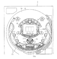
以下、本発明の実施例について詳細に説明する。図1は、本実施例のパチンコ機GMを示す斜視図である。このパチンコ機GMは、島構造体に着脱可能に装着される矩形枠状の木製外枠1と、外枠1に固着されたヒンジ2を介して開閉可能に枢着される前枠3とで構成されている。この前枠3には、遊技盤5が、裏側からではなく表側から着脱自在に装着され、その前側には、ガラス扉6と前面板7とが夫々開閉自在に枢着されている。
Examples of the present invention will be described in detail below. FIG. 1 is a perspective view showing a pachinko machine GM of the present embodiment. This pachinko machine GM includes a rectangular frame-shaped wooden
ガラス扉6の外周には、LEDランプなどによる電飾ランプが、略C字状に配置されている。前面板7には発射用の遊技球を貯留する上皿8が装着され、前枠3の下部には、上皿8から溢れ出し又は抜き取った遊技球を貯留する下皿9と、発射ハンドル10とが設けられている。発射ハンドル10は発射モータと連動しており、発射ハンドル10の回動角度に応じて動作する打撃槌によって遊技球が発射される。
On the outer periphery of the
上皿8の外周面には、チャンスボタン11が設けられている。このチャンスボタン11は、遊技者の左手で操作できる位置に設けられており、遊技者は、発射ハンドル10から右手を離すことなくチャンスボタン11を操作できる。このチャンスボタン11は、通常時には機能していないが、ゲーム状態がボタンチャンス状態となると内蔵ランプが点灯されて操作可能となる。なお、ボタンチャンス状態は、必要に応じて設けられるゲーム状態である。
A
上皿8の右部には、カード式球貸し機に対する球貸し操作用の操作パネル12が設けられ、カード残額を3桁の数字で表示する度数表示部と、所定金額分の遊技球の球貸しを指示する球貸しスイッチと、ゲーム終了時にカードの返却を指令する返却スイッチとが設けられている。
On the right side of the
図2に示すように、遊技盤5には、金属製の外レールと内レールとからなるガイドレール13が環状に設けられ、その内側の遊技領域5aの略中央には、液晶カラーディスプレイDISPが配置されている。また、遊技領域5aの適所には、図柄始動口15、大入賞口16、複数個の普通入賞口17(大入賞口16の左右に4つ)、通過口であるゲート18が配設されている。これらの入賞口15〜18は、それぞれ内部に検出スイッチを有しており、遊技球の通過を検出できるようになっている。
As shown in FIG. 2, the
液晶ディスプレイDISPは、大当り状態に係わる特定図柄を変動表示すると共に背景画像や各種のキャラクタなどをアニメーション的に表示する装置である。この液晶ディスプレイDISPは、中央部に特別図柄表示部Da〜Dcと右上部に普通図柄表示部19を有している。そして、特別図柄表示部Da〜Dcでは、大当り状態の招来を期待させるリーチ演出が実行されたり、特別図柄表示部Da〜Dc及びその周りでは、当否結果を不確定に報知する予告演出などが実行される。 The liquid crystal display DISP is a device that variably displays a specific symbol related to a big hit state and displays a background image and various characters in an animated manner. This liquid crystal display DISP has special symbol display portions Da to Dc in the center portion and a normal symbol display portion 19 in the upper right portion. And, in the special symbol display parts Da to Dc, a reach effect is executed that expects a big hit state to be invited, or in the special symbol display parts Da to Dc and the surroundings, a notice effect that informs the result of the success / failure is executed. Is done.
普通図柄表示部19は普通図柄を表示するものであり、ゲート18を通過した遊技球が検出されると、普通図柄が所定時間だけ変動し、遊技球のゲート18の通過時点において抽出された抽選用乱数値により決定される停止図柄を表示して停止するようになっている。
The normal symbol display unit 19 displays a normal symbol. When a game ball that has passed through the
図柄始動口15は、左右1対の開閉爪15aを備えた電動式チューリップで開閉されるよう例えば構成され、普通図柄表示部19の変動後の停止図柄が当り図柄を表示した場合には、開閉爪15aが所定時間だけ、若しくは、所定個数の遊技球を検出するまで開放されるようになっている。
For example, the symbol start opening 15 is configured to be opened and closed by an electric tulip having a pair of left and right opening and closing
図柄始動口15に遊技球が入賞すると、特別図柄表示部Da〜Dcの表示図柄が所定時間だけ変動し、図柄始動口15への遊技球の入賞タイミングに応じた抽選結果に基づいて決定される停止図柄で停止する。なお、特別図柄表示部Da〜Dc及びその周りでは、一連の図柄演出の間に、予告演出が実行される場合がある。
When a game ball wins the symbol start
大入賞口16は、例えば前方に開放可能な開閉板16aで開閉制御されるが、特別図柄表示部Da〜Dcの図柄変動後の停止図柄が「777」などの大当り図柄のとき、「大当りゲーム」と称する特別遊技が開始され、開閉板16aが開放されるようになっている。なお、特別遊技のラウンド数として、8ラウンド、16ラウンドなど各種の遊技態様が設けられている。ここで、規定ラウンド数が多いほど遊技者に有利である。
The big winning
大入賞口16の開閉板16aが開放された後、所定時間が経過し、又は所定数(例えば10個)の遊技球が入賞すると開閉板16aが閉じる。このような動作は、最大で上記した規定ラウンド数の特別遊技が継続され、遊技者に有利な状態に制御される。なお、特別図柄表示部Da〜Dcの変動後の停止図柄が特別図柄のうちの特定図柄であった場合には、特別遊技の終了後のゲームが高確率状態(以下、確変状態という)となるという特典が付与される。
After the opening /
図3は、上記した各動作を実現するパチンコ機GMの全体回路構成を示すブロック図である。図中の一点破線は、主に、直流電圧ラインを示している。 FIG. 3 is a block diagram showing an overall circuit configuration of the pachinko machine GM that realizes the above-described operations. A dashed line in the figure mainly indicates a DC voltage line.
図示の通り、このパチンコ機GMは、AC24Vを受けて各種の直流電圧やシステムリセット信号(電源リセット信号)SYSなどを出力する電源基板20と、遊技制御動作を中心統括的に担う主制御基板21と、主制御基板21から受けた制御コマンドCMDに基づいてランプ演出及び音声演出を実行する演出制御基板22と、演出制御基板22から受けた制御コマンドCMD’に基づいて液晶ディスプレイDISPを駆動する液晶制御基板23と、主制御基板21から受けた制御コマンドCMD”に基づいて払出モータMを制御して遊技球を払い出す払出制御基板24と、遊技者の操作に応答して遊技球を発射させる発射制御基板25と、を中心に構成されている。
As shown in the figure, this pachinko machine GM is provided with a
但し、この実施例では、主制御基板21が出力する制御コマンドCMDは、コマンド中継基板26と演出インタフェイス基板27を経由して、演出制御基板22に伝送される。また、演出制御基板22が出力する制御コマンドCMD’は、演出インタフェイス基板27を経由して、液晶制御基板23に伝送され、主制御基板21が出力する制御コマンドCMD”は、主基板中継基板28を経由して、払出制御基板24に伝送される。
However, in this embodiment, the control command CMD output from the
これら主制御基板21、演出制御基板22、液晶制御基板23、及び払出制御基板24には、ワンチップマイコンを備えるコンピュータ回路がそれぞれ搭載されている。そこで、これらの制御基板21〜24に搭載された回路、及びその回路によって実現される動作を機能的に総称して、本明細書では、主制御部21、演出制御部22、液晶制御部23、及び払出制御部24と言うことがある。なお、演出制御部22、液晶制御部23、及び払出制御部24の全部又は一部がサブ制御部である。
The
ところで、このパチンコ機GMは、図3の破線で囲む枠側部材GM1と、遊技盤5の背面に固定された盤側部材GM2とに大別されている。枠側部材GM1には、ガラス扉6や前面板7が枢着された前枠3と、その外側の木製外枠1とが含まれており、機種の変更に拘わらず、長期間にわたって遊技ホールに固定的に設置される。一方、盤側部材GM2は、機種変更に対応して交換され、新た盤側部材GM2が、元の盤側部材の代わりに枠側部材GM1に取り付けられる。なお、枠側部材1を除く全てが、盤側部材GM2である。
By the way, the pachinko machine GM is roughly divided into a frame side member GM1 surrounded by a broken line in FIG. 3 and a board side member GM2 fixed to the back of the
図3の破線枠に示す通り、枠側部材GM1には、電源基板20と、払出制御基板24と、発射制御基板25と、枠中継基板32とが含まれており、これらの回路基板が、前枠3の適所に各々固定されている。一方、遊技盤5の背面には、主制御基板21、演出制御基板22、液晶制御基板23が、液晶ディスプレイDISPやその他の回路基板と共に固定されている。そして、枠側部材GM1と盤側部材GM2とは、一箇所に集中配置された接続コネクタC1〜C4によって電気的に接続されている。
As shown in the broken line frame in FIG. 3, the frame-side member GM1 includes a
電源基板20は、接続コネクタC2を通して、主基板中継基板28に接続され、接続コネクタC3を通して、電源中継基板30に接続されている。そして、主基板中継基板28は、電源基板20から受けたシステムリセット信号SYS、RAMクリア信号DEL、電圧降下信号、バックアップ電源BAK、DC12V、DC32Vを、そのまま主制御部21に出力している。同様に、電源中継基板30も、電源基板20から受けたシステムリセット信号SYSや、交流及び直流の電源電圧を、そのまま演出インタフェイス基板27に出力している。なお、演出インタフェイス基板27は、受けたシステムリセット信号SYSを、そのまま演出制御部22と液晶制御部23に出力している。
The
一方、払出制御基板24は、中継基板を介することなく、電源基板20に直結されており、主制御部21が受けると同様の、システムリセット信号SYS、RAMクリア信号DEL、電圧降下信号、バックアップ電源BAKを、その他の電源電圧と共に直接的に受けている。
On the other hand, the
ここで、電源基板20が出力するシステムリセット信号SYSは、電源基板20に交流電源24Vが投入されたことを示す電源リセット信号であり、この電源リセット信号によって各制御部21〜24のワンチップマイコンその他のIC素子が電源リセットされるようになっている。
Here, the system reset signal SYS output from the
主制御部21及び払出制御部24が、電源基板20から受けるRAMクリア信号DELは、各制御部21,24のワンチップマイコンの内蔵RAMの全領域を初期設定するか否かを決定する信号であって、係員が操作する初期化スイッチSWTのON/OFF状態に対応した値を有している。
The RAM clear signal DEL received from the
主制御部21及び払出制御部24が、電源基板20から受ける電圧降下信号は、交流電源24Vが降下し始めたことを示す信号であり、この電圧降下信号を受けることによって、各制御部21、24では、停電や営業終了に先立って、必要な終了処理を開始するようになっている。また、バックアップ電源BAKは、営業終了や停電により交流電源24Vが遮断された後も、主制御部21と払出制御部24のワンチップマイコンの内蔵RAMのデータを保持するDC5Vの直流電源である。したがって、主制御部21と払出制御部25は、電源遮断前の遊技動作を電源投入後に再開できることになる(電源バックアップ機能)。このパチンコ機では少なくとも数日は、各ワンチップマイコンのRAMの記憶内容が保持されるよう設計されている。
The voltage drop signal received from the
一方、演出制御部22と液晶制御部23には、上記した電源バックアップ機能が設けられていない。しかし、先に説明した通り、演出制御部22と液晶制御部23には、電源中継基板30と演出インタフェイス基板27を経由して、システムリセット信号SYSが共通して供給されており、他の制御部21,24と、ほぼ同期したタイミングで電源リセット動作が実現される。
On the other hand, the
図示の通り、主制御部21は、主基板中継基板28を経由して、払出制御部25に制御コマンドCMD”を送信する一方、払出制御部25からは、遊技球の払出動作を示す賞球計数信号や、払出動作の異常に係わるステイタス信号CONを受信している。ステイタス信号CONには、例えば、補給切れ信号、払出不足エラー信号、下皿満杯信号が含まれる。
As illustrated, the
また、主制御部21は、直接的に、或いは、遊技盤中継基板29を経由して、遊技盤5の各遊技部品に接続されている。そして、遊技盤上の各入賞口16〜18に内蔵された検出スイッチのスイッチ信号を受ける一方、電動式チューリップなどのソレノイド類を駆動している。図示の通り、入賞スイッチ信号SGは、直接、主制御部21に伝送され、その他のスイッチ信号は、遊技盤中継基板29を経由して、主制御部21に伝送されている。
Further, the
図4は、主制御部21のワンチップマイコン21Aの内部構成の一部を図示したものである。ここでは、図柄始動口15の検出スイッチSWから入賞スイッチ信号SGを受ける部分も含めて図示している。図示の通り、ワンチップマイコン21Aは、Z80CPU(Zilog社)相当のCPUコア(以下CPUという)と、Z80CTC(counter timer circuit )相当のカウンタ・タイマ回路CTCと、ROM及びRAMのメモリ回路と、ウォッチドッグタイマWDTと、乱数生成回路GNRと、入力ポートINPとを内蔵して構成されている。
FIG. 4 illustrates a part of the internal configuration of the one-
図4に示す通り、検出スイッチSWからの入賞スイッチ信号SGは、バッファ回路BUFを経由して、ワンチップマイコン21Aの乱数生成回路GNRに供給されている。また、入力ポートINPには、大入賞口16や普通入賞口17やゲート18などの検出スイッチからのスイッチ信号が供給されている。
As shown in FIG. 4, the winning switch signal SG from the detection switch SW is supplied to the random number generation circuit GNR of the one-
ところで、バッファ回路BUFは、オープンコレクタ型の出力部を有し、入力側が12Vにプルアップされ、出力側が5Vにプルアップされている。そして、遊技球が図柄始動口15を通過して検出スイッチSWが入賞状態(ON状態)となると、バッファ回路BUFは、正論理のON信号として、入賞スイッチ信号SGを出力する。
By the way, the buffer circuit BUF has an open collector type output section, and the input side is pulled up to 12V and the output side is pulled up to 5V. When the game ball passes through the symbol start
ここで、入賞スイッチ信号SGのパルス幅(遊技球の通過時間T)は、遊技球の通過速度と、遊技球を検知する検出スイッチSWの検出範囲とで規定される。例えば、検出スイッチSWによる遊技球の検出範囲がhである場合に、初速度0の遊技球がt=0から自然落下すると仮定すると、t=Tのタイミングの落下速度Vが、V=gTとなり(g:重力加速度)、1/2mV2=mghの関係から、パルス幅T=SQR(2h/g)となり、仮にh=3mmであればパルス幅はT≒24.7mS、h=5mmであればT≒31.9mSとなる。 Here, the pulse width of the winning switch signal SG (game ball passing time T) is defined by the passing speed of the game ball and the detection range of the detection switch SW for detecting the game ball. For example, assuming that the detection range of a game ball by the detection switch SW is h, and assuming that a game ball with an initial velocity of 0 naturally falls from t = 0, the fall velocity V at the timing of t = T becomes V = gT. (G: Gravity acceleration) and 1/2 mV 2 = mgh, the pulse width T = SQR (2h / g). If h = 3 mm, the pulse width should be T≈24.7 mS, h = 5 mm. T≈31.9 mS.
図4及び図5(a)に示す通り、乱数生成回路GNRは、入賞スイッチ信号SGなどのスイッチ信号を受けてラッチパルスLTを出力するラッチ制御回路30と、システムクロックCLK及び外部クロックXCLKを2分周する分周回路31と、2分周された2種類のクロック信号の何れか一方を更新クロックΦとして選択する選択回路32と、更新クロックΦに基づいて動作するN個の数列生成部33からなる数列生成群33Gと、ラッチ制御回路30から受けるラッチパルスLTに基づいて数列生成部33の生成値を取得する複数のラッチ回路34からなるラッチ群34Gと、各部の動作を規定する制御パラメータや各部の動作状態を示す動作ステイタスを保持する制御レジスタ群35Gと、数列生成部33の動作異常を検出する異常検出回路36と、を含んで構成されている。
As shown in FIGS. 4 and 5A, the random number generation circuit GNR receives a switch signal such as a winning switch signal SG and outputs a latch pulse LT, a system clock CLK, and an external clock XCLK. A
なお、図4には図5には記載していないが、乱数生成回路GNRの各部の動作は、ワンチップマイコン21AのCPUコアとは別の専用プロセッサによって制御されている。但し、本明細書でCPUと称する場合には、ワンチップマイコン21AのCPUコアを意味し、専用プロセッサを意味しない。
Although not shown in FIG. 5 in FIG. 4, the operation of each part of the random number generation circuit GNR is controlled by a dedicated processor different from the CPU core of the one-
ラッチ制御回路30は、複数M個のスイッチ信号が供給可能に構成され、M種類のラッチパルスLTが独立的に出力可能に構成されている。そして、このラッチ制御回路30の構成に対応して、ラッチ群34Gを構成するラッチ回路34の個数は、数列生成部33の個数のM倍であるN×M個である。また、このN×M個のラッチ回路34に対応して、ラッチ回路34からラッチデータを受けるラッチレジスタ35(図5(a)の35b,35d参照)も合計N×M個存在する。
The
したがって、本実施例の乱数生成回路GNRによれば、図柄始動口15や普通入賞口17のスイッチ信号を含んだ合計M種類のスイッチ信号に基づいて、M×N個の乱数値を生成することもでき、抽選処理の豊富化によって遊技内容を豊富化することができる。但し、この実施例では、便宜上、ラッチ制御回路30に供給されるスイッチ信号は、入賞スイッチ信号SGだけであると簡素化している。
Therefore, according to the random number generation circuit GNR of this embodiment, M × N random number values are generated based on a total of M types of switch signals including the switch signals of the symbol start
上記した通り、ラッチ群34Gを構成するN×M個のラッチ回路34は、数列生成群33Gを構成するN個の数列生成部33と、M種類のスイッチ信号とに対応している。そして、制御レジスタ群35Gには、N×M個のラッチ回路34に対応して、N×M個のラッチレジスタ(35b,35dなど)が設けられ、N個の数列生成部33に対応してN個の乱数レジスタ(35a,35cなど)が設けられている。
As described above, the N ×
例えば、図5(a)に示す乱数レジスタ35aや乱数レジスタ35cは、合計N個の乱数レジスタの一部であり、また、図5(a)に示すラッチレジスタ35bやラッチレジスタ35dは、合計N×M個のラッチレジスタの一部である。
For example, the random number register 35a and the random number register 35c illustrated in FIG. 5A are a part of a total of N random number registers, and the
そして、CPUは、ラッチレジスタ35bやラッチレジスタ35dなど、所望のラッチレジスタをアクセスすることで、ラッチ回路34にラッチされた数列生成部33の生成値を取得できるように構成されている。なお、この実施例では、ラッチレジスタ(35bや35dなど)の記憶値がCPUに読み出されると、ラッチレジスタ(35bや35dなど)の記憶値は、自動的にゼロクリアされるよう構成されている。
The CPU is configured to obtain the generated value of the
また、本実施例の制御レジスタ群35Gには、N個の乱数レジスタ(35aや35cなど)を含むので、CPUが、乱数レジスタ35aや乱数レジスタ35cなどの乱数レジスタをアクセスすることで、N個の数列生成部33が生成する数値列の瞬時値を、何時でも把握できることになる。したがって、本実施例によれば、ラッチレジスタ(35b、35dなど)をアクセスして抽選用乱数値を特定できるだけでなく、乱数レジスタ(35a、35cなど)をアクセスして抽選用乱数値を特定することもできる。
In addition, since the
また、CPUは、制御レジスタ群35Gに適宜な制御パラメータを書込むことで、乱数生成回路GNRの動作内容を制御することができる。また、異常検出回路36やラッチ制御回路30の動作状態など、乱数生成回路GNRの内部動作状態は、制御レジスタ群35Gの一部であるステイタスレジスタ35eのステイタス値をCPUが読み出すことで把握可能に構成されている。
Further, the CPU can control the operation content of the random number generation circuit GNR by writing an appropriate control parameter to the
ここで、ステイタスレジスタ35eのステイタス値には、N個の数列生成部33についてのNビットのエラー情報が含まれている。そのため、CPUは、ステイタスレジスタ35eのステイタス値(エラー情報)を読み出すことで、全ての数列生成部33について、その異常の有無を確認することができる。
Here, the status value of the status register 35 e includes N-bit error information for the N
また、このNビットのステイタス値(エラー情報)は、CPUの読み出し動作に対応してゼロクリアされ、正常状態を示す値(=0)に変更されるよう構成されている。そのため、CPUは、ステイタスレジスタ35eのステイタス値(エラー情報)を、例えば、定期的に繰り返し読み出すことで、異常事態が自然復帰したか、或いは、自然復帰しない致命的な異常事態であるかを判断することができる。なお、異常検出回路36が検出する数列生成部33の異常には、動作停止などの深刻なエラーだけでなく、更新クロックΦの周波数のずれなどの軽微なエラーも含まれている。
The N-bit status value (error information) is cleared to zero and changed to a value (= 0) indicating a normal state in response to a CPU read operation. Therefore, the CPU, for example, periodically reads out the status value (error information) of the status register 35e to determine whether the abnormal situation has returned to the natural state or is a fatal abnormal state that does not return spontaneously. can do. Note that the abnormality of the
また、ステイタスレジスタ35eのステイタス値には、N×M個のラッチレジスタ(35bや35dなど)が、ラッチデータを保持しているか否かのラッチ情報も含まれている。このラッチ情報は、N×M個のラッチレジスタ毎に、ラッチデータの有無が1ビット(0/1)で規定され、合計でN×Mビットとなる。 The status value of the status register 35e includes latch information indicating whether or not N × M latch registers (35b, 35d, etc.) hold latch data. In this latch information, the presence or absence of latch data is defined by 1 bit (0/1) for each of N × M latch registers, and the total is N × M bits.
そして、このステイタス値(ラッチ情報)は、読み書き可能に構成されており、CPUは、ステイタスレジスタ35eから所定のラッチレジスタ(35bや35dなど)に対するラッチ情報を読み出すことで、そのラッチレジスタが有意なデータを保持しているか否かを判定することができる。 The status value (latch information) is configured to be readable and writable. The CPU reads the latch information for a predetermined latch register (35b, 35d, etc.) from the status register 35e, so that the latch register is significant. It can be determined whether or not data is held.
そして、有意なデータを保持しているラッチレジスタ(35bや35dなど)から、CPUがラッチデータを読み出すことで、CPUは、抽選処理用の乱数値を取得できることになる。なお、ラッチレジスタ(35bや35dなど)から、ラッチデータを読み出すと、当該ラッチレジスタのデータが自動的にゼロクリアされることは前記した通りである。 When the CPU reads the latch data from a latch register (such as 35b or 35d) that holds significant data, the CPU can acquire a random value for the lottery process. As described above, when latch data is read from a latch register (35b, 35d, etc.), the data in the latch register is automatically cleared to zero.
ところで、ラッチ情報についてのステイタス値は、書込み可能にも構成されており、所定のラッチレジスタについてのステイタス値(ラッチ情報)として、ゼロを書込むことで、当該ラッチレジスタのラッチデータを意図的にゼロクリアすることもできるよう構成されている。 By the way, the status value for latch information is configured to be writable, and by writing zero as the status value (latch information) for a predetermined latch register, the latch data of the latch register is intentionally written. It is configured so that it can be cleared to zero.
この構成は、ラッチレジスタ(35bや35dなど)から、抽選用の乱数値を取得する場合であって、且つ、ラッチレジスタを上書き禁止モード(図6(f))で機能させる場合に特に意義を有する。なお、上書き禁止モードでは、後述するように、ラッチレジスタ(35bや35dなど)がゼロクリアされていない限り、その後のラッチパルスLTに拘わらず、ラッチデータを取得できない。一方、抽選用の乱数値を読み出すと、ラッチレジスタが自動的にゼロクリアされるので、その後は、次のラッチパルスLTに同期してラッチデータが一度だけ取得される。 This configuration is particularly significant when a random number value for lottery is acquired from a latch register (35b, 35d, etc.), and when the latch register functions in the overwrite prohibition mode (FIG. 6 (f)). Have. In the overwrite prohibition mode, as will be described later, unless the latch register (35b, 35d, etc.) is cleared to zero, latch data cannot be acquired regardless of the subsequent latch pulse LT. On the other hand, when the random number for lottery is read, the latch register is automatically cleared to zero, and thereafter, the latch data is acquired only once in synchronization with the next latch pulse LT.
そのため、抽選用の乱数値が読み出された後も、入賞スイッチ信号SGがONレベルを維持する場合には、ラッチレジスタには、同じ入賞スイッチ信号SGに対する次のラッチデータが書き込まれ、その後の上書きが禁止されることになる。なお、入賞スイッチ信号SGのパルス幅が20〜30mSであると仮定すると、このような事態は当然に発生し、今回の入賞スイッチ信号SGがOFFレベルに戻った後も、ラッチレジスタが上書き禁止状態を継続することになる。なお、この上書き禁止状態では、当該ラッチレジスタに対するステイタスレジスタ35eのステイタス値(ラッチ情報)はON状態(=1)である。 For this reason, when the winning switch signal SG is maintained at the ON level even after the random number value for the lottery is read, the next latch data for the same winning switch signal SG is written in the latch register. Overwriting is prohibited. Assuming that the pulse width of the winning switch signal SG is 20 to 30 mS, such a situation naturally occurs. Even after the current winning switch signal SG returns to the OFF level, the latch register is in an overwrite-inhibited state. Will continue. In this overwriting prohibition state, the status value (latch information) of the status register 35e for the latch register is in the ON state (= 1).
そこで、例えば、今回の入賞スイッチ信号SGがOFF状態に遷移したタイミングで、CPUが、当該ラッチレジスタに対するステイタスレジスタ35eのステイタス値(ラッチ情報)として、ゼロを書込むことで、当該ラッチレジスタのデータをゼロクリアすれば、その後のラッチ動作が可能となり、上記の弊害を解消することができる。 Therefore, for example, when the winning switch signal SG of this time transitions to the OFF state, the CPU writes zero as the status value (latch information) of the status register 35e for the latch register, so that the data of the latch register If zero is cleared to zero, the subsequent latch operation can be performed, and the above-described adverse effects can be solved.
図5に戻って説明を続けると、図5(a)に示す通り、入賞スイッチ信号SGは、ラッチ制御回路30だけでなく、制御レジスタ群35Gを構成する信号入力レジスタ35fにも供給されており、CPUは、信号入力レジスタ35fをアクセスすることで、いつでも、入賞スイッチ信号SGのレベルを把握できるようになっている。なお、信号入力レジスタ35fは、この実施例では、入賞スイッチ信号SGのON/OFF状態を記憶するRSフリップフロップで構成されている(図6(B)、図6(C)参照)。
Returning to FIG. 5 and continuing the description, as shown in FIG. 5A, the winning switch signal SG is supplied not only to the
次に、数列生成群33Gを構成するN個の数列生成部33は、詳細には、X個の8ビット長の数列生成部CT8と、Y個の16ビット長の数列生成部CT16とに区分され(N=X+Y)、各々、更新クロックΦの立上りエッジに同期して数値列を更新している。また、全N個の数列生成部33は、任意に設定された数値範囲で数値列を生成する可変長の数列生成部VCTと、規定の数値範囲(0〜2n−1)で数値列を生成する固定長の数列生成部FCTとに各々細分されている。
Next, the N number
ここで、8ビット固定長の数列生成部FCT8は、0〜255の数値範囲の数値列を生成し、16ビット固定長の数列生成部FCT16は、0〜65535の数値範囲の数値列を生成するが、ランダムな初期値から出発して、所定の出現パターンに基づき、飛び飛びの数値を採りながら、28個又は216個の数値を出現されて固定の数値範囲を一巡する。そして、その後は、別の初期値から出発して、別の出現パターンに基づいて同じ動作を繰り返す。 Here, the 8-bit fixed length sequence generator FCT 8 generates a numeric sequence in the numerical range of 0-255, and the 16-bit fixed length sequence generator FCT 16 generates a numerical sequence in the numerical range of 0-65535. while generating, starting from a random initial value, based on a predetermined occurrence pattern, while adopting a number of discrete, it is the appearance of two 8 or 2 16 numbers to cycle the numerical range of fixed. Then, after that, starting from another initial value, the same operation is repeated based on another appearance pattern.
このような固定長の数列生成部FCTは、ワンチップマイコン21Aが電源リセットされると、直ちに、ランダムな初期値から更新動作を開始する。そして、CPUがWDTなどに基づいて異常リセットされても更新動作が停止されることなく、上記のランダムな更新動作を繰り返すので、数値列を推定することが事実上不可能となっている。すなわち、何らかの方法で、数値列の出現パターンや初期値を知ることができ、且つ、大当り抽選の抽選値Hitを知ることができた場合に、意図的にCPUを異常リセットさせても無駄であり、仮に、ワンチップマイコン21Aを電源リセットさせても、電源リセットからCPUが数列生成部33の数値を取得するまでの時間は、正確には一定化しないので、意図的に大当り状態を出現させることは不可能である。
Such a fixed-length sequence generator FCT starts an update operation from a random initial value as soon as the power supply of the one-
以上、固定長の数列生成部FCTについて説明したが、可変長の数列生成部VCTは、規定の制御レジスタ35に任意に設定した最大値を上限値として、0〜最大値の任意の数値範囲で数値列を生成する。数値列の生成動作は、固定長の数列生成部FCTと同じであり、可変長の数列生成部VCTについても、ランダムな初期値から出発して、所定の出現パターンに基づき飛び飛びの数値を採りながら、設定された数値範囲を一巡する。そして、その後は、別の初期値から出発して、別の出現パターンに基づいて同じ動作を繰り返す。 Although the fixed-length sequence generator FCT has been described above, the variable-length sequence generator VCT has a maximum value arbitrarily set in the prescribed control register 35 as an upper limit value, in an arbitrary numerical range of 0 to the maximum value. Generate numeric columns. The generation operation of the numeric sequence is the same as that of the fixed-length sequence generation unit FCT, and the variable-length sequence generation unit VCT starts from a random initial value and takes a jumping numerical value based on a predetermined appearance pattern. Cycle through the set numerical range. Then, after that, starting from another initial value, the same operation is repeated based on another appearance pattern.
可変長の数列生成部VCTは、ワンチップマイコン21Aが電源リセットされない限り、CPUが異常リセットされても更新動作が停止されることなく、上記のランダムな更新動作を繰り返す。この点では、固定長の数列生成部FCTの動作と同じである。しかし、ワンチップマイコン21Aが電源リセットされた場合には、可変長の数列生成部VCTは、規定の制御レジスタ35に最大値を設定した後に更新動作を開始する点で、固定長の数列生成部FCTより、ややセキュリティレベルが下がる。
The variable-length sequence generator VCT repeats the above random update operation without stopping the update operation even when the CPU is abnormally reset, unless the one-
但し、その反面、可変長の数列生成部VCTによれば、生成する数値列の数値範囲を適宜に設定して、抽選処理における当選確率を正確に規定できる利点がある。可変長の数列生成部VCTによれば、生成する数値列の数値範囲の最大値を、例えば199に設定するだけで、当選確率を正確に1/200にすることができる。また、固定長の数列生成部FCTは更新クロックΦを受ける毎に、その立上りエッジに同期して数値列を更新するが、可変長の数列生成部VCTは、規定個数(適宜な素数で規定)の更新クロックを受けるまでは、それまでの数値を維持し、最後の更新クロックΦの立上りエッジに同期して数値列を更新するので、この意味でのランダム性が高まる。 However, the variable-length sequence generator VCT has an advantage that the winning probability in the lottery process can be accurately defined by appropriately setting the numerical range of the numerical sequence to be generated. According to the variable-length sequence generator VCT, the winning probability can be accurately reduced to 1/200 simply by setting the maximum value in the numerical range of the generated numerical sequence to, for example, 199. Each time the fixed-length sequence generator FCT receives the update clock Φ, the numeric sequence is updated in synchronization with the rising edge. However, the variable-length sequence generator VCT has a specified number (specified by an appropriate prime number). Until the update clock is received, the numerical value up to that time is maintained, and the numerical value sequence is updated in synchronization with the rising edge of the last update clock Φ. Therefore, the randomness in this sense increases.
そこで、本実施例では、可変長の数列生成部VCTと固定長の数列生成部FCTのこれらの特徴を考慮して、大当り抽選用の乱数値RNDとしては、16ビット固定長の数列生成部FCT16を使用し、大当り状態において非確変当りか確変当りかを規定する図柄抽選や、特別遊技のラウンド数などの細部についての抽選決定には、8ビット可変長の数列生成部VCT8を使用している。なお、何ら限定されないが、本実施例では8ビット可変長の数列生成部VCT8は、最大値を199に設定することで、0〜199の数値範囲としている。 Therefore, in the present embodiment, in consideration of these characteristics of the variable-length sequence generator VCT and the fixed-length sequence generator FCT, the random number RND for the big hit lottery has a 16-bit fixed-length sequence generator FCT. 16 is used for the lottery determination of details such as the number of rounds of special games and the symbol lottery that specifies whether the odd hit or the odd hit in the big hit state, and the 8-bit variable length sequence generator VCT 8 ing. Although not limited in any way, in this embodiment, the 8-bit variable-length sequence generator VCT 8 sets the maximum value to 199, thereby setting the numerical value range from 0 to 199.
先に説明した通り、可変長の数列生成部VCTは、固定長の数列生成部FCTよりややセキュリティレベルが下がるが、8ビット可変長の数列生成部VCT8は、大当り抽選に当選した後の細部決定に使用されるに過ぎないので、本実施例によれば、8ビット可変長の数列生成部VCT8を使用しても、16ビット固定長の数列生成部FCT16による極めて高いセキュリティレベルが確実に維持される。 As described above, the variable-length sequence generator VCT has a slightly lower security level than the fixed-length sequence generator FCT, but the 8-bit variable-length sequence generator VCT 8 is a detail after winning the big hit lottery. According to the present embodiment, even if the 8-bit variable length sequence generator VCT 8 is used, an extremely high security level is ensured by the 16-bit fixed length sequence generator FCT 16. Maintained.
図5(c)に示す通り、固定長の数列生成部FCT16/FCT8は、更新レジスタR1と、各々適宜な加算値を保持する複数の加算値レジスタR2・・・R2と、複数の加算値レジスタR2・・・R2の何れか一個を選択するアドレス情報を生成するカウンタCTと、選択された加算値レジスタR2と更新レジスタR1の各保有値を加算する加算器ADとを有して構成されている。ここで、加算値レジスタR2・・・R2の個数は2X個であり、カウンタCTのY個の出力ビットのうち、任意に選択されたXビット(Y>X)が、加算値レジスタR2・・・R2を選択するアドレス情報として使用される。 As shown in FIG. 5C, the fixed-length sequence generator FCT 16 / FCT 8 includes an update register R1, a plurality of addition value registers R2... R2, each holding an appropriate addition value, and a plurality of additions. A counter CT for generating address information for selecting any one of the value registers R2... R2, and an adder AD for adding the respective added values of the selected addition value register R2 and the update register R1. Has been. Here, the number of additional value register R2 · · · R2 is 2 X number, among the Y output bits of the counter CT, arbitrarily chosen X bits (Y> X) is, the additional value register R2 · .. Used as address information for selecting R2.
なお、図5(c)では、説明の便宜上、ハードウェアとして加算器ADや2X個の加算値レジスタR2・・・R2が存在するよう記載しているが、好適には、加算器ADの機能は、専用プロセッサによって実現される。また、実際の加算値レジスタR2は、乱数生成回路GNRのメモリ(不図示)に記憶された加算値で代用される。 In FIG. 5C, for convenience of description, it is described that there are an adder AD and 2 X addition value registers R2... R2 as hardware. The function is realized by a dedicated processor. Further, the actual addition value register R2 is substituted with an addition value stored in a memory (not shown) of the random number generation circuit GNR.
そして、加算器ADの加算結果が、更新レジスタR1に保存されるよう構成されており、選択される加算値レジスタR2は、更新クロックΦに同期して変更される。また、加算器ADは、16ビット長又は8ビット長の加算器であり、更新クロックΦに同期して機能している。したがって、更新レジスタR1の値がDA1で、その時に選択された加算値レジスタR2の値がDA2である場合には、R1←DA1+DA2の演算が、16ビット長又は8ビット長の加算演算として実行される。 The addition result of the adder AD is stored in the update register R1, and the selected addition value register R2 is changed in synchronization with the update clock Φ. The adder AD is a 16-bit or 8-bit adder and functions in synchronization with the update clock Φ. Therefore, when the value of the update register R1 is DA1 and the value of the addition value register R2 selected at that time is DA2, the operation of R1 ← DA1 + DA2 is executed as an addition operation of 16-bit length or 8-bit length. The
本実施例では、各加算値レジスタR2・・・R2の保有値を適宜に設定することで、28個又は216個の更新クロックΦを受けると、それまでに生成された数値列が数値範囲(0〜216−1又は28−1)を一巡するよう構成されている。そして、更新レジスタR1は、電源投入時や、28個又は216個の更新クロックΦを受けた後に、適宜な初期値に変更されることで、『ランダムな初期値から出発して、所定の出現パターンに基づき飛び飛びの数値を採りながら、設定された数値範囲を一巡する動作』を実現している。また、28個又は216個の更新クロックΦを受けた後に、カウンタCTのY個の出力ビットのうち(Y>X)、選択されるXビットが適宜に変更されることで、加算値レジスタR2・・・R2の選択順序が変わり、出現パターンが変更される。 In this embodiment, by setting the retention value of the addition value register R2 · · · R2 suitably, 2 8 or 2 when 16 receives the update clock [Phi, numerical numerical sequence generated so far The range (0 to 2 16 −1 or 2 8 −1) is configured to make a round. Then, the update registers R1 is and when the power is turned on, after receiving the 2 8 or 2 16 update clocks [Phi, by being changed to an appropriate initial value, starting from "a random initial value, a predetermined Based on the appearance pattern of, the operation to go around the set numerical range while taking the jumping numerical value is realized. Further, after receiving 2 8 or 2 16 update clocks [Phi, of Y output bits of the counter CT (Y> X), by X bits selected is changed as appropriate, the additional value The selection order of the registers R2... R2 changes, and the appearance pattern is changed.
可変長の数列生成部VCT16/VCT8についても基本構成は同じであるが、更新タイミングを規定するカウンタCT’が付加されている(破線部参照)。カウンタCTは、更新クロックΦを規定回数(適宜な素数に設定)受けることを条件に、そのキャリ信号CYによって加算器ADを動作させており、この結果、規定個数の更新クロックΦを受けるまでは、それまでの数値を維持する変則動作が実現される。 The basic structure of the variable-length sequence generators VCT 16 / VCT 8 is the same, but a counter CT ′ that defines the update timing is added (see the broken line part). The counter CT operates the adder AD with the carry signal CY on condition that the update clock Φ is received a specified number of times (set to an appropriate prime number), and as a result, until the specified number of update clocks Φ is received. An anomalous operation that maintains the previous values is realized.
また、可変長の数列生成部VCT16/VCT8には、加算結果が設定された数値範囲(0〜MAX)に含まれるよう補正部AMが設けられ(破線部参照)、加算器ADの出力ビットのうち、上限値MAXを超えない必要ビット部分だけが使用される。そして、加算結果SUMが上限値MAXを超える場合には、SUM←SUM−MAXの補正演算が実行される。 Further, the variable length sequence generator VCT 16 / VCT 8 is provided with a correction unit AM (see the broken line portion) so that the addition result is included in the set numerical range (0 to MAX), and the output of the adder AD Of the bits, only the necessary bit portion that does not exceed the upper limit value MAX is used. When the addition result SUM exceeds the upper limit value MAX, a correction calculation of SUM ← SUM-MAX is executed.
以上、数列生成部33について、内部構成の一例を極めて簡略化して説明したが、実際には、セキュリティレベルを上げるべく更に複雑な構成になっている。
As described above, the example of the internal configuration of the
図5(a)に示す通り、16ビット固定長の数列生成部41aには、専用プロセッサに制御されて16ビット長の数値のビット並びを適宜に入れ替える転置回路42が接続されている。そして、固定長の数列生成部FCT41aや転置回路42は、16ビットの転置パターンやランダムな初期値を付与する計数制御部40aに制御されて動作している。なお、計数制御部40aは、制御レジスタ群35Gの所定の制御レジスタに設定された制御パラメータに基づいて動作し、数列生成部41aの異常状態は、ステイタスレジスタ35eのステイタス値(エラー情報)として記憶される。
As shown in FIG. 5A, the 16-bit fixed length sequence generator 41a is connected to a
図5(a)に示す通り、転置回路42の出力は、16ビットラッチ回路34と共に、制御レジスタ群35Gの乱数レジスタ35aにも供給されており、CPUは何時でも乱数レジスタ35aの16ビット値を取得できるようになっている。
As shown in FIG. 5A, the output of the
8ビット可変長の数列生成部41b(VCT8)についても同様であり、8ビット可変長の数列生成部41b(VCT8)は、計数制御部40bに制御されて、所定の数値範囲(0〜199)で数値列を生成し、一巡毎にランダムな初期値に基づいて更新動作を繰り返している。この計数制御部40bも、制御レジスタ群35Gの所定の制御レジスタに設定された制御パラメータ(最大値など)に基づいて数列生成部41bの更新動作を制御し、数列生成部41bの異常状態は、ステイタスレジスタ35eのステイタス値(エラー情報)として記憶される。
The same applies to the 8-bit variable-length sequence generation unit 41b (VCT 8), 8-bit variable-length sequence generation unit 41b (VCT 8) is controlled by the counting control unit 40b, a predetermined numerical range (0 199), a numerical sequence is generated, and the updating operation is repeated for each round based on a random initial value. The count control unit 40b also controls the update operation of the sequence generator 41b based on a control parameter (such as a maximum value) set in a predetermined control register of the
また、8ビット長の数列生成部41bの出力は、8ビットラッチ回路34と共に、制御レジスタ群35Gの乱数レジスタ35cにも供給されており、CPUは何時でも乱数レジスタ35cの数値を取得できるようになっている。
The output of the 8-bit length sequence generator 41b is also supplied to the random number register 35c of the
図4に示す通り、分周回路31には、CPUの動作を規定するシステムクロックCLKだけでなく、システムクロックCLKとは無関係に動作する外部クロックXCLKが供給可能に構成されている。2つのクロック信号CLK,XCLKは、何れも分周回路31で2分周されて選択回路32に供給され、制御レジスタ35への設定値に基づいて、何れか一方のクロック信号が、16ビット固定長の数列生成部41a(FCT16)用の更新クロックΦとして選択される。なお、16ビット可変長の数列生成部VCT16や、8ビット長の数列生成部FCT8/VCT8については、システムクロックCLKが更新クロックΦとして使用される。
As shown in FIG. 4, the
ところで、本実施例では、16ビット固定長の数列生成部41a(FCT16)が、外部クロックXCLKを使用している状態で、異常検出回路36が数列生成部FCT16の異常動作を検知すると、外部クロックXCLKに代えて、自動的にシステムクロックCLKを使用するよう構成されている。そのため、外部クロックXCLKに異常が生じても、数列生成部FCT16が更新動作を継続できるだけでなく、外部クロックXCLKを悪用した不正行為を未然防止することができる。先に説明した通り、数列生成部FCT16の異常動作は、更新クロックΦの停止だけでなく、例えば、外部クロックXCLKの周波数の異常な低下なども含まれる。 By the way, in the present embodiment, when the 16-bit fixed length sequence generator 41a (FCT 16 ) is using the external clock XCLK and the abnormality detection circuit 36 detects an abnormal operation of the sequence generator FCT 16 , Instead of the external clock XCLK, the system clock CLK is automatically used. Therefore, even if an abnormality occurs in the external clock XCLK, the sequence generator FCT 16 can not only continue the update operation, but also prevent illegal acts that abuse the external clock XCLK. As described above, the abnormal operation of the sequence generator FCT 16 includes not only the stop of the update clock Φ but also an abnormal decrease in the frequency of the external clock XCLK, for example.
何れにしても、外部クロックXCLKは、システムクロックCLKと非同期とすべきであるが、その周波数は、内部動作の安定化の観点から、システムクロックCLKと同程度の周波数とすべきであり、好ましくは、システムクロックCLKの周波数の0.8〜1.6倍の程度の周波数に設定される。なお、特に限定されないが、実施例の場合には、システムクロックCLKの周波数は20MHz程度である。 In any case, the external clock XCLK should be asynchronous with the system clock CLK, but its frequency should be the same as that of the system clock CLK from the viewpoint of stabilization of the internal operation. Is set to a frequency of about 0.8 to 1.6 times the frequency of the system clock CLK. Although not particularly limited, in the case of the embodiment, the frequency of the system clock CLK is about 20 MHz.
本実施例では、上記の通り、外部クロックXCLKが使用可能であるが、セキュリティ上の観点から数列生成部FCT16の更新動作をシステムクロックCLKに同期させないため、外部クロックXCLKを更新クロックΦとして使用するのが好適である。一方、外部クロックXCLKの発振回路を省略する簡易構成を採りたいとの観点からは、システムクロックCLKを更新クロックΦに使用するのが好適である。 In this embodiment, as described above, the external clock XCLK can be used. However, from the viewpoint of security, the update operation of the sequence generator FCT 16 is not synchronized with the system clock CLK, so the external clock XCLK is used as the update clock Φ. It is preferable to do this. On the other hand, it is preferable to use the system clock CLK as the update clock Φ from the viewpoint of adopting a simple configuration that omits the oscillation circuit of the external clock XCLK.
そこで、本実施例では、遊技機の機種毎に何れの動作態様を採るかを、任意に選択できるようジャンパー線J1,J2を設け(図4参照)、以下の3つの動作態様(a)〜(c)を任意に選択可能にしている。 Therefore, in the present embodiment, jumper wires J1 and J2 are provided so as to be able to arbitrarily select which operation mode to use for each model of gaming machine (see FIG. 4), and the following three operation modes (a) to (a) to (C) can be arbitrarily selected.
例えば、ジャンパー線J2を切断する機種(a)では、外部クロックXCLKが数列生成部FCT16用の更新クロックΦに選択され、ジャンパー線J1を切断する機種(b)では、システムクロックCLKが更新クロックΦに選択されるよう制御レジスタ35に制御パラメータが設定される。また、ジャンパー線J1,J2を維持した状態で、外部クロックXCLKを供給することなく、その入力端子INをプルダウンする機種(c)では(破線部参照)、外部クロックXCLKが数列生成部FCT16用の更新クロックΦに選択されるよう、制御レジスタ35に制御パラメータが設定される。なお、この第3の機種(c)では、外部クロックXCLKが供給されていない以上、実際には、バイパス経路Bypassを通過したシステムクロックCLKが使用されるのは勿論である。
For example, in the model (a) that cuts the jumper line J2, the external clock XCLK is selected as the update clock Φ for the sequence generator FCT 16 , and in the model (b) that cuts the jumper line J1, the system clock CLK is the update clock. A control parameter is set in the
第3の機種(c)では、万一、バイパス経路Bypass上の配線パターンなどに異常が生じた場合でも、数列生成部FCT16の異常動作を検出した異常検出回路36によって、自動的にノーマル経路NormalのシステムクロックCLKが使用されるので、引き続き数列生成部FCT16を正常に動作させることができる。この場合、動作移行時に周波数の変化がないので極めて自然な移行動作を実現することができる。そこで、本実施例は、第3の機種(c)として構成されている。したがって、全ての数列生成部33の更新クロックΦは、システムクロックCLKを2分周したものとなる。
In the third model (c), even if an abnormality occurs in the wiring pattern on the bypass path Bypass, the normal path is automatically automatically detected by the abnormality detection circuit 36 that detects the abnormal operation of the sequence generator FCT 16. Since the normal system clock CLK is used, the sequence generator FCT 16 can continue to operate normally. In this case, since there is no frequency change at the time of operation transition, a very natural transition operation can be realized. Therefore, this embodiment is configured as a third model (c). Therefore, the update clock Φ of all the
次に、図5と図6に基づいてラッチ制御回路30と、ラッチレジスタ(35bや35dなど)の動作について説明する。なお、このラッチ制御回路30には、複数のスイッチ信号が供給可能であるが、先に説明した通り、入賞スイッチ信号SGだけが供給されているとする(M=1)。但し、他のスイッチ信号が供給されている場合(M≠1)でも以下と同様の動作が実現される。
Next, the operation of the
図6Aに示す通り、この実施例では、入賞スイッチ信号SGのON/OFFレベルは、更新クロックΦの立下りエッジで判定され(図6A(b)参照)、更新クロックΦの立上りエッジで、全N個の数列生成部33の生成値が、各々の出現パターンに基づいて更新される(図6A(c)参照)。なお、数列生成部33の種類毎に、数値列の数値範囲や更新タイミングが異なるだけでなく、出現する数値列の出現パターンや、出現パターンの初期値が各々相違するので、N個の数列生成部33の数値列は、原則として各々相違する。
As shown in FIG. 6A, in this embodiment, the ON / OFF level of the winning switch signal SG is determined at the falling edge of the update clock Φ (see FIG. 6A (b)). The generation values of the N number
このような数列生成部33の更新動作に並行して、ラッチ制御回路30は、入賞スイッチ信号SGが連続して所定時間ONレベルを維持するか否かを判定しており、例えば、更新クロックΦで計測して128回連続してONレベルを維持することを条件にラッチパルスLTを出力するよう構成されている(図6A(d)参照)。本実施例は、このような判定動作を設けているので、スパイク状のノイズを入賞スイッチ信号SGであると誤認するおそれがない。
In parallel with the updating operation of the
本実施例の場合、図4に示すバイパス経路Bypassを通過する20MHz程度のシステムクロックCLKが2分周されて更新クロックΦとなるので、更新クロックΦは10MHz程度である。したがって、ラッチパルスLTが出力される場合には、少なくとも、入賞スイッチ信号SGが連続して128/106=128μS程度、継続してONレベルを維持したことが担保され、ノイズによる影響を排除することができ、また、ノイズを悪用した不正遊技を排除することができる。 In the case of the present embodiment, the system clock CLK of about 20 MHz passing through the bypass path Bypass shown in FIG. 4 is divided by two to become the update clock Φ, so the update clock Φ is about 10 MHz. Therefore, when the latch pulse LT is output, it is ensured that at least the winning switch signal SG continuously maintains the ON level for about 128/10 6 = 128 μS, and the influence of noise is eliminated. It is also possible to eliminate fraudulent games that abuse noise.
このようにしてラッチ制御回路30で生成されたラッチパルスLTは、ラッチ群34Gを構成するN×M個のラッチ回路34に供給され、各ラッチ回路34は、自らに対応する数列生成部33の生成値を、ラッチパルスLTに同期して取得保持し、これをそのままN×M個のラッチレジスタ(図5の35bや35dなど)に出力する(図6A(e)(f)参照)。
The latch pulse LT generated in this way by the
但し、本実施例の場合、更新クロックΦは、10MHz程度であり、入賞スイッチ信号SGのパルス幅Tは、30mS程度であるため、数列生成部33の生成値がラッチ回路34にラッチされた後も、引き続き入賞スイッチ信号SGはON状態を維持することになる。したがって、その後も、128μS程度の時間間隔で、繰り返しラッチパルスLTがラッチ回路に出力される。
However, in this embodiment, the update clock Φ is about 10 MHz, and the pulse width T of the winning switch signal SG is about 30 mS, so that the generated value of the
このような動作を考慮して、本実施例では、ラッチレジスタ(35bや35d)を上書き禁止モード(図6A(e))で使用するか、上書き許可モード(図6A(f))で使用するかを、任意に選択可能に構成している。上書き禁止モードとは、ラッチレジスタ(35bや35dなど)のラッチデータが、CPUに読み取られてクリアされるまでは、ラッチ回路34の出力データを受け付けない動作モードを意味する。このような動作モードを採る場合には、CPUによるラッチレジスタの数値取得タイミングが遅れた場合でも、入賞スイッチ信号SGのONエッジに近接したタイミングにおける数列生成部33の生成値を取得できる意義がある。なお、図6A(e)には、最初に取得された数値Xが抽選用乱数値に使用されることを示している。そして、数値Xが取得されたことで、ラッチレジスタ(35bや35d)がゼロクリアされ、ステイタスレジスタ35eのステイタス値もゼロとなる(図6A(g))。
In consideration of such an operation, in this embodiment, the latch registers (35b and 35d) are used in the overwrite prohibition mode (FIG. 6A (e)) or in the overwrite permission mode (FIG. 6A (f)). These can be arbitrarily selected. The overwrite prohibition mode means an operation mode in which the output data of the
これに対して上書き許可モードとは、ラッチ回路34の出力データが常に受け付けられる動作モードであり、ラッチ回路34がラッチパルスLTを受ける毎に、ラッチレジスタ(35bや35dなど)が、新規の数値を取得し直す動作モードを意味する。このような動作モードを採る場合には、CPUの取得タイミングが遅れた場合、入賞スイッチ信号SGのONエッジから大きく(例えば数10mS程度)離れたタイミングの数値を取得することになる。
On the other hand, the overwrite permission mode is an operation mode in which the output data of the
この場合には、例え、違法遊技者が、最適タイミング狙って入賞スイッチ信号SGをON動作させたとしても、実際に取得される数値を、違法遊技者の意図する値に近づけることはできない点が利点である。なお、図6A(f)には、最初に取得された数値Xが、次に、数値Yに置き換わり、その後も次々と変化して、最終的にラッチされた数値が抽選用乱数値に使用されることを示している。なお、図示例では、数値Yが取得されたことで、ラッチレジスタ(35bや35d)がゼロクリアされ、ステイタスレジスタ35eのステイタス値もゼロとなることを示している(図6A(g))。 In this case, for example, even if the illegal player turns on the winning switch signal SG for the optimal timing, the actually acquired numerical value cannot be brought close to the value intended by the illegal player. Is an advantage. In FIG. 6A (f), the numerical value X acquired first is then replaced with the numerical value Y, and then changes one after another, and the finally latched numerical value is used as the random number for lottery. Which indicates that. In the illustrated example, when the numerical value Y is acquired, the latch registers (35b and 35d) are cleared to zero, and the status value of the status register 35e is also zero (FIG. 6A (g)).
上書き禁止モードも、上書き許可モードも、各々、十分に意義を有しているが、本実施例では、ラッチレジスタ(図5の35bや35dなど)を使用することなく、16ビット乱数レジスタ35aと8ビット乱数レジスタ35cに基づいて、抽選用乱数値を特定している。それは、ラッチレジスタ(図5の35bや35dなど)がゼロクリアされた後も、ラッチパルスLTに基づいて、ラッチレジスタにラッチデータが保存されることに対応して、ステイタスレジスタ35eのステイタス値がセットされ、このステイタス値を、新規の入賞スイッチ信号SGであると誤認するおそれがあるためである。 Both the overwrite prohibition mode and the overwrite permission mode are sufficiently significant, but in this embodiment, the 16-bit random number register 35a is used without using a latch register (35b and 35d in FIG. 5). Based on the 8-bit random number register 35c, the random number for lottery is specified. This is because the status value of the status register 35e is set in response to the latch data being stored in the latch register based on the latch pulse LT even after the latch register (35b, 35d in FIG. 5) is cleared to zero. This is because the status value may be mistaken for the new winning switch signal SG.
但し、この問題は、入賞スイッチ信号SGのONエッジを監視するだけで十分に解消できるので、上書きモードや上書き禁止モードで機能するラッチレジスタの意義が否定される訳ではなく、各々、優れた効果を発揮することに変わりはない。 However, since this problem can be sufficiently solved by simply monitoring the ON edge of the winning switch signal SG, the significance of the latch register functioning in the overwrite mode or the overwrite prohibit mode is not denied, There is no change in demonstrating.
以上を確認した上で、乱数レジスタ35a,35cに基づいて、抽選用乱数値を特定する実施例について説明する。なお、実施例では、乱数レジスタ35a,35cに基づいて抽選用乱数値を特定するが、16ビットラッチ回路34の出力を受けるラッチレジスタ35b(一個又は複数個)、及び/又は、8ビットラッチ回路34の出力を受けるラッチレジスタ35d(一個又は複数個)を、CPUがアクセスして抽選用乱数値を特定してもよく、むしろ、その方が典型的である。
After confirming the above, an embodiment for specifying the random number for lottery based on the random number registers 35a and 35c will be described. In the embodiment, the random number for lottery is specified based on the random number registers 35a and 35c, but the
何れにしても、16ビット長の乱数レジスタ35aは,図5(b)に示す通り、16ビット長のDラッチ50と、各8ビット長のバスバッファ51L,51Hと、負論理ORゲート52と、を有して構成されている。乱数レジスタ35aは、このように、1バイト単位で数値を保持するが、この構成に関連して、乱数レジスタ35aには、連続する2つのアドレス値NN,NN+1が付番されている。 In any case, the 16-bit random number register 35a includes a 16-bit D latch 50, 8-bit bus buffers 51L and 51H, a negative logic OR gate 52, as shown in FIG. , And is configured. As described above, the random number register 35a holds a numerical value in units of 1 byte. In relation to this configuration, the random number register 35a is assigned two consecutive address values NN and NN + 1.
なお、これらの点は、16ビット長のラッチレジスタ35bについても同様であり、16ビット長のDラッチと、各8ビット長のバスバッファ2個と、負論理ORゲートとを有して構成され、連続する2つのアドレス値NN’,NN’+1が付番されている。なお、乱数レジスタ35aやラッチレジスタ35bが、2バイトデータを1バイト毎に扱うのは、Z80相当のCPUのデータバスD0−D7が1バイト幅であるためであり、また、CPUに内蔵された汎用レジスタ群W,A,B,C,D,E,H,Lが各々1バイトデータを扱う構成になっているためである(図5(a)参照)。
These points also apply to the 16-bit
なお、汎用レジスタ群のうち、IX,IYのデータ幅は16ビット長であり、プログラムカウンタPCからアドレスバスA0−A15に出力されるアドレスデータも16ビット長である。そして、上記したアドレス値NN,NN’は、アドレスバスA0−A15を経由してアドレスデコーダ37に供給されることで、適宜なデコード信号DECが生成され、何れかの制御レジスタ35がデコード信号DECによって選択されることになる。なお、この実施例では、アドレスバスA0−A15の下位8ビットA0−A7が、データバスD0−D7と共用されている。 In the general-purpose register group, the data width of IX and IY is 16 bits long, and the address data output from the program counter PC to the address bus A0-A15 is also 16 bits long. The address values NN and NN ′ described above are supplied to the address decoder 37 via the address buses A0 to A15, whereby an appropriate decode signal DEC is generated, and any one of the control registers 35 receives the decode signal DEC. Will be selected. In this embodiment, the lower 8 bits A0-A7 of the address bus A0-A15 are shared with the data bus D0-D7.
さて、図5(b)に示す乱数レジスタ35aに説明を戻すと、NN番地と、NN+1番地に付番されたバスバッファ51L,51Hは、アドレスデコーダ37が出力する選択信号によって選択される。なお、一方の選択信号は、アドレスバスA0−A15の値が、NNの場合にアクティブレベル(Lレベル)となり、他方の選択信号は、アドレスバスA0−A15の値が、NN+1の場合にアクティブレベル(Lレベル)となる。そして、2つの選択信号は、負論理ORゲート52に供給されるので、負論理ORゲート52が出力するデコード信号DECは、2つの選択信号の何れか、或いは、双方がLレベルの時にLレベルとなる。 Returning to the random number register 35a shown in FIG. 5B, the bus buffers 51L and 51H assigned to the address NN and the address NN + 1 are selected by the selection signal output from the address decoder 37. One selection signal has an active level (L level) when the value of the address bus A0-A15 is NN, and the other selection signal has an active level when the value of the address bus A0-A15 is NN + 1. (L level). Since the two selection signals are supplied to the negative logic OR gate 52, the decode signal DEC output from the negative logic OR gate 52 is at the L level when either or both of the two selection signals are at the L level. It becomes.
Dラッチ50は、図5(c)に示す回路構成を16個設けて構成されている。そして、Dラッチ50は、転置回路42が出力する転置処理後の数値CT0−CT15とデコード信号DECとを受けて動作している。具体的には、デコード信号DECを共通的に受ける16個のMOSトランジスタQ1と、NOTゲート(16個)を経由してデコード信号DECを受ける16個のMOSトランジスタQ2と、MOSトランジスタQ2のソース端子とドレイン端子を接続するNOTゲート(2×16個)とを有して構成されている。
The D latch 50 is configured by providing 16 circuit configurations shown in FIG. The D latch 50 operates by receiving the transposed numerical values CT0 to CT15 output from the transposing
Dラッチ50は、上記の通りに構成されているので、デコード信号DECがHレベルの場合には、トランジスタQ1がON状態で、トランジスタQ2がOFF状態となり、逆に、デコード信号DECがLレベルの場合には、トランジスタQ1がOFF状態で、トランジスタQ2がON状態となる。 Since the D latch 50 is configured as described above, when the decode signal DEC is at the H level, the transistor Q1 is in the ON state, the transistor Q2 is in the OFF state, and conversely, the decode signal DEC is at the L level. In this case, the transistor Q1 is turned off and the transistor Q2 is turned on.
そのため、デコード信号DECがHレベルの場合には、転置回路42の出力である16ビット長の数値CTi(IN)が、トランジスタQ1と2つのNOTゲートを通過して、そのレベルのままで出力信号CTi(OUT)となる。一方、デコード信号DECがLベルになると、トランジスタQ1がOFF状態となるので、転置回路42の出力は伝送されず、MOSトランジスタQ1の浮遊容量に蓄積されている直前の入力データが、トランジスタQ2を通過して出力される。
Therefore, when the decode signal DEC is at the H level, the 16-bit length numerical value CTi (IN) that is the output of the
したがって、この回路構成によれば、デコード信号DECをLレベルに遷移させることで、バスバッファ51L,51Hに伝送する数値CTiを固定化することができる。言い換えると、デコード信号DEC=Lの状態で、CPUがバスバッファ51L,51Hをアクセスすれば、同一の数値の上位バイトと下位バイトを安定して取得できることになる。 Therefore, according to this circuit configuration, the numerical value CTi transmitted to the bus buffers 51L and 51H can be fixed by shifting the decode signal DEC to the L level. In other words, if the CPU accesses the bus buffers 51L and 51H in the state of the decode signal DEC = L, the upper byte and lower byte of the same numerical value can be stably acquired.
以上、16ビット長の乱数レジスタ35aについて説明したが、8ビット長の乱数レジスタ35cの回路構成も、基本的に乱数レジスタ35aと同じである。すなわち、乱数レジスタ35cは、8ビット長のDラッチと、8ビット長のバスバッファと、負論理ORゲートと、を有して構成されている。但し、乱数レジスタ35cは、転置回路を経由することなく8ビット長の数列生成部41bの値を受けており、これを保持するバスバッファが単一個であることに対応して、乱数レジスタ35cには、単一のアドレス値が付番されている。 The 16-bit random number register 35a has been described above, but the circuit configuration of the 8-bit random number register 35c is basically the same as that of the random number register 35a. That is, the random number register 35c includes an 8-bit D latch, an 8-bit bus buffer, and a negative logic OR gate. However, the random number register 35c receives the value of the 8-bit length sequence generation unit 41b without going through the transposition circuit, and the random number register 35c has a single bus buffer to hold it. Are numbered with a single address value.
続いて、ラッチパルスLT(図6A(d))を出力するラッチ制御回路30の要部について説明する。ラッチ制御回路30は、図6Cに示すノイズ除去回路を含んで構成されており、ノイズ除去回路は、2つの128進カウンタCT1,CT2と、入賞スイッチ信号SGを正論理と負論理で受ける2つのANDゲートG1,G2と、NOTゲートG3とで構成されている。ここで、2つのANDゲートG1,G2には、各々、更新クロックΦが供給されている。
Next, the main part of the
そして、カウンタCT1のキャリ出力CYは、ラッチパルスLTとして各ラッチ回路34に供給され、各カウンタCT1,CT2のキャリ出力CY,CYは、信号入力レジスタ35fのセット端子Sとリセット端子Rとに供給されている。図6Cに示す通り、本実施例では、信号入力レジスタ35fの1ビット分は、RSフリップフロップで構成されている。
The carry output CY of the counter CT1 is supplied as a latch pulse LT to each
そして、入賞スイッチ信号SGは、ANDゲートG1と共に、カウンタCT1のクリア端子CLRに供給されているので、入賞スイッチ信号SGがLレベルであると、カウンタCT1のカウント値はゼロ状態を維持することになる。一方、入賞スイッチ信号SGは、NOTゲートG3を経由して、ANDゲートG2と共に、カウンタCT2のクリア端子に供給されている。 Since the winning switch signal SG is supplied to the clear terminal CLR of the counter CT1 together with the AND gate G1, if the winning switch signal SG is at the L level, the count value of the counter CT1 is maintained at the zero state. Become. On the other hand, the winning switch signal SG is supplied to the clear terminal of the counter CT2 together with the AND gate G2 via the NOT gate G3.
本実施例のノイズ除去回路(図6C)は、上記の通りに構成されているので、入賞スイッチ信号SG=Hであれば、カウンタCT1が更新クロックΦに基づいてカウントアップされ、128個目の更新クロックΦを受けると、ラッチパルスLTたるキャリ信号CYが出力される。そして、その後も、128個目の更新クロックΦを受ける毎に、ラッチパルスLTが繰り返し出力される(図6A(d)参照)。 Since the noise removal circuit (FIG. 6C) of the present embodiment is configured as described above, if the winning switch signal SG = H, the counter CT1 is counted up based on the update clock Φ, and the 128th When the update clock Φ is received, a carry signal CY as a latch pulse LT is output. Thereafter, every time the 128th update clock Φ is received, the latch pulse LT is repeatedly output (see FIG. 6A (d)).
また、カウンタCT1のキャリ信号CYは、信号入力レジスタ35f(RSフリップフロップ)のセット端子Sにも供給されているので、連続して128個の更新クロックΦを受けることを条件に、信号入力レジスタ35fの記憶値がHレベルとなる。なお、図6Bは、入賞スイッチ信号SGと、更新クロックΦと、信号入力レジスタ35fの記憶値との関係を図示したものである。 Since the carry signal CY of the counter CT1 is also supplied to the set terminal S of the signal input register 35f (RS flip-flop), the signal input register is provided on the condition that 128 update clocks Φ are continuously received. The stored value of 35f becomes H level. FIG. 6B illustrates the relationship among the winning switch signal SG, the update clock Φ, and the stored value of the signal input register 35f.
ところで、このようなカウンタCT1のカウント動作中に、入賞スイッチ信号SG=Lとなると、カウンタ動作が初期状態に戻るので、結局、更新クロック128個分の間、入賞スイッチ信号SGが継続してHレベルであることを条件に、信号入力レジスタ35fがHレベルになり、ラッチパルスLTが出力されることになる。したがって、入賞スイッチ信号SGに誤認される可能性のあるスパイクノイズの影響が排除される。図6Bには、入賞スイッチ信号SG=Lの状態で、Hレベルのノイズが重畳される状態を図示しているが、このようなHレベルのノイズによってラッチパルスLTが出力されたり、信号入力レジスタ35fの記憶値が変化するおそれはない。 By the way, when the winning switch signal SG = L during the counting operation of the counter CT1, the counter operation returns to the initial state, so that the winning switch signal SG continues to be H for 128 update clocks. On condition that the signal is at the level, the signal input register 35f becomes H level, and the latch pulse LT is output. Therefore, the influence of spike noise that may be mistaken for the winning switch signal SG is eliminated. FIG. 6B shows a state in which the H level noise is superimposed in the state where the winning switch signal SG = L, but the latch pulse LT is output by such H level noise or the signal input register. There is no possibility that the stored value of 35f changes.
次に、信号入力レジスタ35fに記憶された入賞スイッチ信号SGも、やがて、数10mS後にはLレベルに戻る。そして、入賞スイッチ信号SGがOFFレベルに遷移した後は、カウンタCT2が計数動作を開始して、128個目の更新クロックΦを受けると、カウンタCT2からキャリ信号CYが出力される。このキャリ信号CYは、信号入力レジスタ35f(RSフリップフロップ)のリセット端子Rに供給されているので、カウンタCT2からのキャリ信号CYの出力に同期して、信号入力レジスタ35fの記憶値がLレベルに戻ることになる。 Next, the winning switch signal SG stored in the signal input register 35f also returns to the L level after several tens of milliseconds. Then, after the winning switch signal SG transitions to the OFF level, the counter CT2 starts the counting operation, and when the 128th update clock Φ is received, the carry signal CY is output from the counter CT2. Since the carry signal CY is supplied to the reset terminal R of the signal input register 35f (RS flip-flop), the stored value of the signal input register 35f is L level in synchronization with the output of the carry signal CY from the counter CT2. Will return.
このように、本実施例では、入賞スイッチ信号SGがHレベルである場合だけでなくLレベルである場合にも、それが所定時間(更新クロック128個分)継続することを条件に、信号入力レジスタ35fに取得するので、ノイズによる悪影響を確実に排除することができる。 As described above, in this embodiment, the signal input is performed on the condition that the winning switch signal SG is not only at the H level but also at the L level on the condition that it continues for a predetermined time (128 update clocks). Since the data is acquired by the register 35f, it is possible to reliably eliminate the adverse effects due to noise.
すなわち、入賞スイッチ信号SGがONレベルになった後に、スパイクノイズが重畳しても、入賞スイッチ信号SGがOFFレベルになったと誤認されるおそれがなく、したがって、入賞スイッチ信号SGのON遷移から、相当遅れて信号入力レジスタ35fがアクセスされても、その遅れが大きく(例えば30mS以上で)ない限り、入賞スイッチ信号SGを読み落とすことがない。なお、図6Bには、入賞スイッチ信号SG=Hの状態で、Lレベルのノイズが重畳される状態を図示しているが、このようなLレベルのノイズによって、信号入力レジスタ35fの記憶値が変化するおそれはない。 That is, even if spike noise is superimposed after the winning switch signal SG becomes ON level, there is no possibility that the winning switch signal SG is mistakenly assumed to be OFF level. Therefore, from the ON transition of the winning switch signal SG, Even if the signal input register 35f is accessed with considerable delay, the winning switch signal SG is not missed unless the delay is large (for example, 30 mS or more). FIG. 6B shows a state where L level noise is superimposed in the state where the winning switch signal SG = H, but the stored value of the signal input register 35f is caused by such L level noise. There is no risk of change.
以上、ノイズの影響を排除して入賞スイッチ信号SGのレベルを把握できる構成を説明したが、本実施例では、CPUのソフウェア処理を全く使用することなく、ノイズ除去効果を達成することに大きな価値がある。 As described above, the configuration in which the level of the winning switch signal SG can be grasped while eliminating the influence of noise has been described. However, in this embodiment, it is of great value to achieve the noise removal effect without using any CPU software processing. There is.
すなわち、プログラム処理によって上記と同様の動作を実現することは可能ではあるが、そのような手法を採るとCPUの処理負担が増して肝心の遊技制御に悪影響が及ぶ。また、この種の遊技機では、主制御部のROMの使用容量に厳しい制限があるので、ROMの記憶容量を無駄使いすることも問題があるが、本実施例によれば、ROMの記憶容量を全く消費することなく、上記した優れた耐ノイズ性能を発揮する。 That is, it is possible to realize the same operation as described above by the program processing, but if such a method is adopted, the processing load on the CPU increases and the important game control is adversely affected. In addition, in this type of gaming machine, there is a problem in that the ROM storage capacity is wasted because there is a strict limit on the ROM usage capacity of the main control unit, but according to this embodiment, the ROM storage capacity The above-described excellent noise resistance performance is exhibited without consuming any of the above.
続いて、図7に基づいて、CPUが、16ビット長の乱数レジスタ35aの数値を読み出すread動作について説明する。図7(b)は、システムクロックCLKが2分周されて生成された更新クロックΦを示しており、更新クロックΦの立上りエッジで、16ビット長の固定長の数列生成部FCT16である数列生成部41a(図5(a)参照)が更新されることを示している。図7(a)は、数列生成部41aの数値を示しており、説明の便宜上、出現パターンが単純なインクリメント更新(+1)であって、M→M+1と更新されることにしている。 Next, a read operation in which the CPU reads the numerical value of the 16-bit random number register 35a will be described with reference to FIG. FIG. 7B shows an update clock Φ generated by dividing the system clock CLK by 2, and a sequence that is a 16-bit fixed-length sequence generator FCT 16 at the rising edge of the update clock Φ. It shows that the generation unit 41a (see FIG. 5A) is updated. FIG. 7A shows the numerical values of the sequence generator 41a. For convenience of explanation, the appearance pattern is a simple increment update (+1) and is updated from M → M + 1.
また、以下の説明では、一例として、16ビットデータのロード命令LD WA,(HL)について説明する。なお、このロード命令の実行に先行して、HLレジスタには、乱数レジスタ35aの先頭アドレス値である16ビットデータNNが記憶されている。 In the following description, a 16-bit data load instruction LDWA, (HL) will be described as an example. Prior to the execution of this load instruction, the HL register stores 16-bit data NN which is the head address value of the random number register 35a.
ロード命令LD WA,(HL)は、HLレジスタが指示するアドレス値NNに付番されたレジスタの記憶値(乱数レジスタ35aの下位1バイト記憶値)をAレジスタに取得すると共に、NN+1に付番されたレジスタの記憶値(乱数レジスタ35aの上位1バイト記憶値)をWレジスタに取得する命令である。このロード命令は、1バイト長のオペコードと、1バイト長のオペランドに区分される2バイト命令であり、システムクロックCLKを4サイクル使用して実行を終えるよう構成されている。 The load instruction LD WA, (HL) acquires the storage value of the register numbered by the address value NN indicated by the HL register (lower one byte storage value of the random number register 35a) in the A register and is numbered NN + 1. This is an instruction for acquiring the stored value of the registered register (the upper one byte stored value of the random number register 35a) in the W register. This load instruction is a 2-byte instruction divided into a 1-byte length opcode and a 1-byte length operand, and is configured to finish execution using four cycles of the system clock CLK.
すなわち、図7(c)〜図7(e)に示す通り、第1サイクル(M1サイクル)で、この命令(LD WA,(HL))の1バイト目が記憶されているメモリのアドレス値(プログラムカウンタPCH・PCLの値)がアドレスバスA0−A15に出力され、CPUにオペコードが取得された後、第2サイクルで、この命令の2バイト目が記憶されているメモリのアドレス値(プログラムカウンタPCH・PCLの値)がアドレスバスA0−A15に出力されてCPUにオペランドが取得される。 That is, as shown in FIG. 7C to FIG. 7E, in the first cycle (M1 cycle), the address value of the memory (1st byte of this instruction (LD WA, (HL)) is stored ( The value of the program counter PC H / PC L ) is output to the address bus A0-A15 and the opcode is acquired by the CPU. Then, in the second cycle, the address value of the memory in which the second byte of this instruction is stored ( the value of the program counter PC H · PC L) is the operand to be output to the address bus A0-A15 CPU is obtained.
そして、その後の第3サイクルでは、アドレスバスA0−A15に16ビットアドレス値NNが出力されて、乱数レジスタ35aの下位1バイト記憶値がAレジスタに取得され、第4サイクルでは、アドレスバスA0−A15に16ビットアドレス値NN+1が出力されて、乱数レジスタ35aの上位1バイト記憶値がWレジスタに取得される。なお、図7(f)〜図7(h)は、CPUからコントロールバスに出力される制御信号であり、各々、M1サイクルであることを示すM1信号(f)、メモリリクエスト信号MREQ(g)、メモリリード信号RD(h)を示している。 In the subsequent third cycle, the 16-bit address value NN is output to the address bus A0-A15, and the lower 1 byte storage value of the random number register 35a is acquired in the A register. In the fourth cycle, the address bus A0- The 16-bit address value NN + 1 is output to A15, and the upper 1-byte stored value of the random number register 35a is acquired in the W register. 7F to 7H are control signals output from the CPU to the control bus. The M1 signal (f) indicating the M1 cycle and the memory request signal MREQ (g), respectively. The memory read signal RD (h) is shown.
また、図7(i)は、乱数レジスタ35aの負論理ORゲート52から出力されるデコード信号DECを示している。先に説明した通り、デコード信号DECは、アドレスバスA0−A15に出力されるアドレス値NNのアドレスデコード値と、アドレス値NN+1のアドレスデコード値の負論理OR値であるから、上記した4サイクルの命令実行中の第3サイクルと第4サイクルだけがLレベルとなり、それ以外のタイミングでは、Hレベルとなる。 FIG. 7 (i) shows the decode signal DEC output from the negative logic OR gate 52 of the random number register 35a. As described above, the decode signal DEC is an address decode value of the address value NN output to the address buses A0 to A15 and a negative logical OR value of the address decode value of the address value NN + 1. Only the third and fourth cycles during execution of the instruction are at the L level, and at other timings, the H level is set.
そのため、乱数レジスタ35aのDラッチ50は、上記した4サイクル動作中の第2サイクルまではON状態であって、転置回路42からの数値CTiをバスバッファ51L,51Hに伝えるが、その後の第3サイクルと第4サイクルは、OFF状態となって、転置回路42からの数値CTiを遮断することになる。したがって、第2サイクルの終了時における転置回路42の出力値が、第3サイクルと第4サイクルの間は、変化することなく維持されることになる。
Therefore, the D latch 50 of the random number register 35a is in the ON state until the second cycle during the above four-cycle operation, and transmits the numerical value CTi from the
このように、本実施例では、乱数レジスタ35aにDラッチ50を設け、そのON/OFF状態をデコード信号DECで制御するので、16ビット長の乱数レジスタ35aなどの制御レジスタに付番されたアドレス情報を、連続してアドレスバスA0−A15に出力する限り、その時の数値を正確に取得することができる。したがって、例えば、+1の出現パターンを採っている16ビット長の数値列が、数値01FFHの状態から0200Hに更新されるタイミングで、乱数レジスタ35aがアクセスされたとしても、CPUに取得される値は、01FFHか0200Hである正常な数値を転置させた値であり、02FFHのような中途半端な数値が転置されて取得されるおそれはない。 Thus, in this embodiment, the D latch 50 is provided in the random number register 35a, and its ON / OFF state is controlled by the decode signal DEC. Therefore, the address assigned to the control register such as the 16-bit long random number register 35a. As long as information is continuously output to the address buses A0 to A15, the numerical value at that time can be obtained accurately. Therefore, for example, even if the random number register 35a is accessed at a timing when a 16-bit numeric value sequence adopting the +1 appearance pattern is updated from the state of the numerical value 01FFH to 0200H, the value acquired by the CPU is , 01FFH or 0200H is a value obtained by transposing a normal numerical value, and there is no possibility that a halfway numerical value such as 02FFH is transposed and acquired.
なお、この動作は、更新クロックΦをシステムクロックCLKから生成するのではなく、外部クロックXCLKから生成した場合も同様に保障される。すなわち、図7(j)に示すように、より高速で、システムクロックと同期しない更新クロックΦを使用した場合でも、デコード信号DECによるDラッチの開閉制御によって、正常な数値であるA+1を転置させた値を取得することができる。 This operation is similarly ensured when the update clock Φ is generated not from the system clock CLK but from the external clock XCLK. That is, as shown in FIG. 7 (j), even when an update clock Φ that is faster and not synchronized with the system clock is used, the normal value A + 1 is transposed by the open / close control of the D latch by the decode signal DEC. Value can be obtained.
これに対して、制御レジスタに付番されたアドレス情報を、アドレスバスA0−A15に連続して出力しないロード命令を使用すると上記のような安定動作が保証されない。図8は、ロード命令LD A,(DE) とロード命令LD W,(HL) を連続される場合を例示している。なお、これらの命令に先行して、DEレジスタにはアドレス値NNが格納され、HLレジスタにはアドレス値NN+1が格納されている。また、説明の都合上、16ビット長の数値列は、+1の出現パターンを採っていることにする。 On the other hand, if a load instruction that does not continuously output the address information assigned to the control register to the address buses A0 to A15 is used, the above stable operation cannot be guaranteed. FIG. 8 illustrates a case where the load instruction LD A, (DE) and the load instruction LD W, (HL) are consecutive. Prior to these instructions, an address value NN is stored in the DE register, and an address value NN + 1 is stored in the HL register. Further, for convenience of explanation, it is assumed that a 16-bit numeric string has an appearance pattern of +1.
このような状態で、ロード命令LD A,(DE) と、ロード命令LD W,(HL) とを連続させても、ロード命令LD A,(DE) の実行後に、不可避的にロード命令LD W,(HL) の命令フェッチサイクル(M1)が入るので、デコード信号DECをLレベルに維持させることができず、その結果として、MやM+1のような正常なアドレス値を転置させた値ではなく、数値Mの下位バイトと、数値M+1の上位バイトを組み合わせた中途半端な数値が転置されてCPUに取得されることになる。 In this state, even if the load instruction LD A, (DE) and the load instruction LD W, (HL) are continued, the load instruction LD W is unavoidable after the execution of the load instruction LD A, (DE). , (HL) instruction fetch cycle (M1) enters, the decode signal DEC cannot be maintained at the L level, and as a result, it is not a value obtained by transposing a normal address value such as M or M + 1. The halfway numerical value combining the lower byte of the numerical value M and the upper byte of the numerical value M + 1 is transposed and acquired by the CPU.
このような場合には、特に、発生する数値列の数値範囲(0〜MAX)が、固定範囲(0〜216)でない場合(MAX<216−1)には、不合理な乱数値RNDを取得してしまうおそれもある。例えば、数値列の上限値MAXがMAX=1150Hの場合に、仮に、10FFHから1134Hへの更新時に乱数値が取得されると、取得された乱数値は、11FFHとなって上限値MAXを超えてしまう。 In such a case, an unreasonable random number value RND particularly when the numerical range (0 to MAX) of the generated numerical sequence is not the fixed range (0 to 2 16 ) (MAX <2 16 −1). There is also a risk of acquiring. For example, when the upper limit value MAX of the numerical sequence is MAX = 1150H, if a random number value is acquired when updating from 10FFH to 1134H, the acquired random number value becomes 11FFH and exceeds the upper limit value MAX. End up.
以上、乱数生成回路GNRについて詳細に説明したので、続いて、図4に示すCPUによって実行される主制御部21の遊技動作を説明する。図9及び図10は、主制御部21の制御プログラムを示すフローチャートであり、電源電圧の復旧や投入に基づいて起動されるシステムリセット処理(図9)と、所定時間毎(4mS)に起動されるマスク可能なタイマ割込み処理(図10)とで構成されている。
The random number generation circuit GNR has been described in detail above. Next, the game operation of the
以下、図9を参照しつつ、システムリセット処理プログラム(メイン処理)について説明する。メイン処理が開始されるのは、停電状態からの復旧時のように初期化スイッチSWTがOFF状態で電源がON状態になる場合と、遊技ホールの開店時のように、初期化スイッチSWTがON操作されて電源がON状態になる場合とがある。なお、ウォッチドッグタイマWDTが起動してCPUが強制的にリセットされる場合もある。 Hereinafter, the system reset processing program (main processing) will be described with reference to FIG. The main process is started when the initialization switch SWT is OFF and the power is turned ON, such as when recovering from a power failure, and when the game hall is opened, the initialization switch SWT is ON. There is a case where the power source is turned on by being operated. In some cases, the watchdog timer WDT is activated and the CPU is forcibly reset.
何れの場合でも、Z80CPUは、最初に、CPU内部のスタックポインタSPの値を、スタック領域の最終アドレスに対応して初期設定する(ST1)。次に、ワンチップマイコンの乱数生成回路GNRの制御レジスタ群35Gを含んだ各種レジスタの値を初期設定する(ST2)。
In any case, the Z80 CPU first initializes the value of the stack pointer SP in the CPU corresponding to the final address of the stack area (ST1). Next, the values of various registers including the
ステップST2の初期設定処理が終われば、入力ポートINPからRAMクリア信号DELを取得する(ST3)。RAMクリア信号DELとは、ワンチップマイコン21Aの内蔵RAMの全領域を初期設定するか否かを決定する信号であって、係員が操作する初期化スイッチSWTのON/OFF状態に対応した値を有している。
When the initial setting process in step ST2 is completed, the RAM clear signal DEL is acquired from the input port INP (ST3). The RAM clear signal DEL is a signal for determining whether or not to initialize all the areas of the built-in RAM of the one-
次にRAMクリア信号DELのレベルが判定されるが(ST4)、RAMクリア信号DELがON状態であったと仮定すると、内蔵RAMの全領域がゼロクリアされる(ST8)。次に、RAM領域がゼロクリアされたことを報知するための制御コマンドを出力する(ST9)。 Next, the level of the RAM clear signal DEL is determined (ST4). Assuming that the RAM clear signal DEL is in the ON state, the entire area of the built-in RAM is cleared to zero (ST8). Next, a control command for notifying that the RAM area has been cleared to zero is output (ST9).
次に、タイマ割込み動作(図10)を起動する割込み信号INTを出力するCTCを初期設定する(ST10)。そして、CPUを割込み禁止状態にセットした状態で(ST11)、必要なカウンタがあれば、これについて更新処理を実行し(ST12)、その後、CPUを割込み許可状態に戻して(ST13)、ステップST11に戻る。 Next, the CTC that outputs the interrupt signal INT for starting the timer interrupt operation (FIG. 10) is initialized (ST10). Then, with the CPU set to the interrupt disabled state (ST11), if there is a necessary counter, update processing is executed for this (ST12), then the CPU is returned to the interrupt enabled state (ST13), and step ST11. Return to.
但し、本実施例では、乱数生成回路GNRから多数の乱数値を取得できるので、ステップST11〜ST13の処理を全て排除することができる。そのため、ST11〜ST13の分だけ、ROMの記憶容量を節約することができ、他の制御処理を豊富化することができる。 However, in this embodiment, since a large number of random values can be acquired from the random number generation circuit GNR, all the processes in steps ST11 to ST13 can be eliminated. Therefore, the storage capacity of the ROM can be saved by the amount of ST11 to ST13, and other control processes can be enriched.
次に、ステップST4の判定処理に戻って説明すると、CPUがウォッチドッグタイマWDTなどによって強制的にリセットされた場合や、停電状態からの復旧時には、RAMクリア信号DELはOFF状態である。そして、このような場合には、ステップST4の判定に続いて、バックアップフラグBFLの内容が判定される(ST5)。バックアップフラグBFLとは、電源監視処理(ST20)においてバックアップ処理が実行されたことを示すデータであり、この実施例では、電源遮断時にバックアップフラグBFLが5AHとされ、電源復帰後のステップST20の処理でゼロクリアされる。 Next, returning to the determination process in step ST4, the RAM clear signal DEL is in the OFF state when the CPU is forcibly reset by the watchdog timer WDT or the like, or when recovering from the power failure state. In such a case, the content of the backup flag BFL is determined following the determination in step ST4 (ST5). The backup flag BFL is data indicating that the backup process has been executed in the power supply monitoring process (ST20). In this embodiment, the backup flag BFL is set to 5AH when the power is shut off, and the process of step ST20 after the power is restored. Is cleared to zero.
そのため、電源投入時や、停電状態からの復旧時である場合には、バックアップフラグBFLの内容が5AHの筈である。但し、何らかの理由でプログラムが暴走状態となり、ウォッチドッグタイマによるCPUリセット動作が生じたような場合には、バックアップフラグBFL=00Hである。したがって、BFL≠5AH(通常はBFL=00H)となる場合には、ステップST5からステップST8の処理に移行させて遊技機の動作を初期状態に戻す。 Therefore, when the power is turned on or when recovering from the power failure state, the content of the backup flag BFL is 5AH. However, if the program goes into a runaway state for some reason and a CPU reset operation is caused by the watchdog timer, the backup flag BFL = 00H. Therefore, when BFL ≠ 5AH (normally BFL = 00H), the process proceeds from step ST5 to step ST8 to return the operation of the gaming machine to the initial state.
一方、バックアップフラグBFL=5AHであれば、チェックサム値を算出するためのチェックサム演算を実行する(ST6)。ここで、チェックサム演算とは、内蔵RAMのワーク領域を対象とする8ビット加算演算である。そして、チェックサム値が算出されたら、この演算結果を、RAMのSUM番地の記憶値と比較をする(ST7)。 On the other hand, if the backup flag BFL = 5AH, a checksum calculation for calculating a checksum value is executed (ST6). Here, the checksum operation is an 8-bit addition operation for the work area of the built-in RAM. When the checksum value is calculated, the calculation result is compared with the stored value at the SUM address in the RAM (ST7).
SUM番地には、電圧降下時に実行される電源監視処理(ST20)において、同じチェックサム演算によるチェックサム値が記憶されている。なお、記憶された演算結果は、内蔵RAMの他のデータと共に、バックアップ電源によって維持されている。したがって、本来は、ステップST7の判定によって両者が一致する筈である。 In the SUM address, a checksum value obtained by the same checksum calculation is stored in the power supply monitoring process (ST20) executed when the voltage drops. The stored calculation result is maintained by a backup power source together with other data of the built-in RAM. Therefore, the two should be matched by the determination in step ST7.
しかし、電源降下時にチェックサム演算の実行できなかった場合や、実行できても、その後、メイン処理のチェックサム演算(ST6)の実行時までの間に、ワーク領域のデータが破損している場合もあり、このような場合にはステップST7の判定結果は不一致となる。 However, if the checksum operation cannot be executed when the power is turned off, or if it can be executed, but the work area data is damaged before the checksum operation (ST6) of the main process is executed. In such a case, the determination result in step ST7 is inconsistent.
そこで、判定結果の不一致によりデータ破損が検出された場合には、ステップST8の処理に移行させてRAMクリア処理を実行し、遊技機の動作を初期状態に戻す。一方、ステップST7の判定において、チェックサム演算(ST8)によるチェックサム値と、SUM番地の記憶値とが一致する場合には、上記したステップST10の処理に移行することになる。 Therefore, if data corruption is detected due to a discrepancy in the determination results, the process proceeds to step ST8, RAM clear processing is executed, and the operation of the gaming machine is returned to the initial state. On the other hand, if it is determined in step ST7 that the checksum value obtained by the checksum calculation (ST8) matches the stored value at the SUM address, the process proceeds to step ST10 described above.
続いて、上記したメイン処理を中断させて、4mS毎に開始されるタイマ割込み処理プログラム(図10)を説明する。タイマ割込みが生じると、CPUのレジスタを保存することなく、直ちに電源監視処理を実行する(ST20)。これは、タイマ割込み処理が起動されるタイミングが、ステップST13の直後に固定されているためである。 Next, a timer interrupt processing program (FIG. 10) started every 4 ms with the main process described above being interrupted will be described. When the timer interrupt occurs, the power supply monitoring process is immediately executed without saving the CPU register (ST20). This is because the timing at which the timer interrupt process is started is fixed immediately after step ST13.
電源監視処理(ST20)では、電源基板20から供給されている電圧降下信号のレベルを判定し、異常レベルであれば、バックアップフラグBAKFLGを5AHに設定し、チェックサム値を算出して、SUM番地に記憶した上で、電源が遮断されるのを待つ。
In the power supply monitoring process (ST20), the level of the voltage drop signal supplied from the
次に、普通図柄処理ST28における抽選処理で使用される当り用カウンタRGを更新する乱数作成処理を実行する(ST21)。当り用カウンタRGは、所定数値範囲内でインクリメント(+1)され、更新後のカウンタの値は、当り判定用乱数値として当否抽選処理で活用される。具体的には、当り用カウンタRGの値は、遊技球がゲート18を通過した場合に、普通図柄処理(ST18)における当り抽選処理で当り用カウンタRGが使用される。
Next, a random number generating process for updating the winning counter RG used in the lottery process in the normal symbol process ST28 is executed (ST21). The winning counter RG is incremented (+1) within a predetermined numerical value range, and the updated counter value is utilized in the winning / not determining lottery process as a winning determination random value. Specifically, as the value of the winning counter RG, when the game ball passes through the
ところで、特別図柄処理(ST32)における大当り抽選処理に使用される抽選用乱数値RNDについては、乱数生成回路GNRから取得するので、ソフトウェア処理で更新されることはない。したがって、この意味でも、本実施例では、ROMの記憶容量を節約することができ、他の制御処理を豊富化することができる。 By the way, since the random number RND for lottery used for the jackpot lottery process in the special symbol process (ST32) is obtained from the random number generation circuit GNR, it is not updated by software processing. Therefore, also in this sense, in this embodiment, the storage capacity of the ROM can be saved, and other control processes can be enriched.
なお、本明細書では、乱数生成回路GNRに関する説明の便宜上、当り用カウンタRGについて、ステップST21の処理で更新しているが、本実施例の乱数生成回路GNRからは、更新クロックΦを共通化するものの、数値が全く関連しない多数の乱数値を取得できるので、実際には、ステップST21の処理を排除するのが好ましく、そうすれば、ROMの記憶容量を更に節約することができる。 In this specification, for convenience of explanation regarding the random number generation circuit GNR, the winning counter RG is updated by the process of step ST21. However, the update clock Φ is shared by the random number generation circuit GNR of the present embodiment. However, since it is possible to obtain a large number of random values whose numerical values are not related at all, it is actually preferable to eliminate the processing of step ST21, and in this case, the storage capacity of the ROM can be further saved.
何れにしても、次に、遊技動作の時間を管理しているタイマについてタイマ減算処理を行う(ST22)。減算されるタイマは、大入賞口16の開放時間や、その他の遊技演出時間を管理するものである。
In any case, next, a timer subtraction process is performed for the timer that manages the game operation time (ST22). The timer to be subtracted manages the opening time of the special winning
このようなタイマ減算処理が終わると、図柄始動口15やゲート18の検出スイッチを含む各種スイッチ類のスイッチ信号を取得して記憶する(ST23)。なお、図柄始動口15に関する入賞スイッチ信号SGは、乱数生成回路GNRの信号入力レジスタ35fをアクセスして取得する。一方、その他の検出スイッチによるスイッチ信号は、ワンチップマイコンの入力ポートINPから取得する。但し、入賞スイッチ信号SG以外のスイッチ信号についても、乱数生成回路GNRの信号入力レジスタ35fを経由させることができ、その方が好ましいことは前述した通りである。
When such a timer subtraction process is completed, switch signals of various switches including the symbol start
そして、何れのスイッチ信号も、今回の取得値と前回の取得値とを対比して、ON状態に遷移したか、或いは、OFF状態に遷移したかが判定され記憶される。従来の遊技機では、ノイズ対策として、スイッチ信号のON遷移やOFF遷移の判定に、複数回の割込み処理に跨った重複判定を要したが、本実施例では、乱数生成回路GNRにノイズ除去回路(図6C)を設けているので、入賞スイッチ信号SGについての重複判定は全く不要である。 Then, for any switch signal, the current acquired value and the previous acquired value are compared, and it is determined and stored whether the transition has been made to the ON state or the OFF state. In the conventional gaming machine, as a countermeasure against noise, the determination of the ON transition and the OFF transition of the switch signal requires duplication determination over a plurality of interrupt processes, but in this embodiment, the random number generation circuit GNR includes a noise removal circuit. Since (FIG. 6C) is provided, it is not necessary to make a duplicate determination for the winning switch signal SG.
すなわち、従来は、割込み処理毎に繰り返し判定して、例えばOFF→ON→ONと推移したことを条件に、入賞スイッチ信号SGがON遷移したと判定していたが、本実施例では、単純にOFF→ONの変化をステップST23の処理で確認できれば、それだけで、入賞スイッチ信号SGがON遷移したと判定することができる。なお、信号入力レジスタ35fを経由させれば、他のスイッチ信号についても同様の判定で足りることになる。 That is, in the past, it was determined repeatedly for each interrupt process, and for example, it was determined that the winning switch signal SG has made an ON transition on the condition that it has transitioned from OFF to ON to ON. If the change from OFF to ON can be confirmed by the processing in step ST23, it can be determined that the winning switch signal SG has been turned ON. If the signal input register 35f is used, the same determination is sufficient for other switch signals.
このように、本実施例では、スイッチ信号がON遷移した2×τ後には、そのスイッチ信号がON遷移したと判定できるので、例えば、制御内容を複雑高度化するべく、割込み周期を大幅に長く設定しても(τ>>4mS)、入賞スイッチ信号SGやその他のスイッチ信号を読み落とすおそれがない。また、重複判定をしなくて良い分だけ、制御プログラムを簡素化でき、その分だけROMの消費量を抑制できる。
In this way, in this embodiment, it can be determined that the switch signal has made an
さて、このようなスイッチ入力処理(ST23)が終わると、エラー管理処理を実行する(ST24)。エラー管理処理とは、遊技球の補給が停止したり、遊技球が詰まっていないかなど、機器内部に異常が生じていないかの判定を意味する。 When such switch input processing (ST23) is completed, error management processing is executed (ST24). The error management process means a determination as to whether an abnormality has occurred inside the device, such as whether or not the supply of game balls has stopped or the game balls are clogged.
また、乱数生成回路GNRに異常が発生していないかの判定を意味する。先に説明した通り、N個全ての数列生成部33・・・33について、その異常の有無は、ステイタスレジスタ35eに記憶されている。したがって、CPUは、ステイタスレジスタ35eを読み出すだけで、数列生成部33が正常に動作しているかを判定することができる。そして、ステイタスレジスタ35eを読み出す毎に、ステイタス値は正常レベルに戻るので、複数回の割込み処理で、数列生成部33に異常が認められる場合には、その異常を報知して制御動作を停止するようにしている(ST40)。
Further, it means a determination as to whether an abnormality has occurred in the random number generation circuit GNR. As described above, the presence / absence of abnormality of all N
エラー管理処理(ST24)が終われば、次に、払出制御部33向けの制御コマンドを作成した後(ST25)、この段階で生成されている制御コマンドを該当するサブ制御部に伝送する(ST26)。 When the error management process (ST24) is finished, next, after creating a control command for the payout control unit 33 (ST25), the control command generated at this stage is transmitted to the corresponding sub-control unit (ST26). .
続いて、現在が当り中の動作モードでないことを条件に、普通図柄処理を実行する(ST28)。普通図柄処理とは、普通電動役物を作動させるか否かの判定を意味し、ステップST23のスイッチ入力結果によって遊技球がゲートを通過していると判定された場合に、乱数生成処理(ST21)で更新された当り用カウンタRGを、当り当選値と対比する。そして、対比結果が当選状態であれば当り中の動作モードに変更する。また、当り中となれば、普通電動役物の作動に向けた処理を行う(ST30)。 Subsequently, the normal symbol process is executed on the condition that the current operation mode is not the hit mode (ST28). The normal symbol process means a determination as to whether or not to operate an ordinary electric accessory, and when it is determined that the game ball has passed through the gate according to the switch input result in step ST23, a random number generation process (ST21). The winning counter RG updated in step) is compared with the winning winning value. If the comparison result is a winning state, the operation mode is changed to the winning operation mode. Further, if it is hit, processing for the operation of the ordinary electric accessory is performed (ST30).
次に、必要な制御コマンドを該当するサブ制御部に伝送し(ST31)、特別図柄処理を行う(ST32)。特別図柄処理とは、大入賞口16など特別電動役物を作動させるか否かの判定であり、大当り抽選処理を含んだ処理である。
Next, a necessary control command is transmitted to the corresponding sub-control unit (ST31), and special symbol processing is performed (ST32). The special symbol process is a determination of whether or not to operate a special electric accessory such as the
具体的な処理としては、ステップST23のスイッチ入力結果によって入賞スイッチ信号SGがON遷移したと判定された場合には、乱数生成回路GNRの乱数レジスタ35aの数値を取得して、大当り抽選用の乱数値RNDとして記憶する。この場合の取得処理としては、単一の命令(フェッチサイクルが単一)で、2バイトデータを取得できるロード命令が使用される。例えば、図7に説明したロード命令LD AW,(HL)が使用され、これに先行して、乱数レジスタ35aを特定するレジスタ番号NN,NN+1についてのロード命令LD HL,NNが使用される。 Specifically, when it is determined that the winning switch signal SG has been turned ON based on the switch input result in step ST23, the numerical value of the random number register 35a of the random number generation circuit GNR is acquired, and the random winning lottery randomness is obtained. Store as numeric RND. As an acquisition process in this case, a load instruction that can acquire 2-byte data with a single instruction (single fetch cycle) is used. For example, the load instruction LD AW, (HL) described in FIG. 7 is used, and prior to this, the load instruction LD HL, NN for the register numbers NN and NN + 1 that specify the random number register 35a is used.
また、乱数レジスタ35cの数値を取得して、図柄抽選用の乱数値RND’として記憶する。先に説明した通り、この実施例では、大当り抽選用の乱数値RNDは、数値範囲(0〜65535)の16ビットデータであり、図柄抽選用の乱数値RND’は、数値範囲(0〜199)の8ビットデータである。したがって、乱数レジスタ35cのアクセスは、1バイト用のロード命令であるLD A,(DE) が使用される。 Further, the numerical value of the random number register 35c is acquired and stored as a random number value RND 'for symbol lottery. As described above, in this embodiment, the random number RND for jackpot lottery is 16-bit data in the numerical range (0 to 65535), and the random value RND ′ for symbol lottery is in the numerical range (0 to 199). ) 8-bit data. Therefore, the random number register 35c is accessed using LDA, (DE), which is a 1-byte load instruction.
そして、このタイミングで、図柄演出処理(図柄表示部Da〜Dcの図柄変動処理)が終了しており、且つ、抽選保留状態の先行する入賞スイッチ信号SGが存在しない場合には、乱数値RNDに基づいて大当り抽選処理を実行し、乱数値RND’に基づいて図柄抽選を実行する(ST32)。大当り抽選処理の当選状態では、図柄抽選処理によって確変当りか否か、及び、特別遊技のラウンド数が決定され、大当り抽選処理の外れ状態では、図柄抽選処理によって外れ図柄が決定される。 At this timing, when the symbol effect processing (the symbol variation processing of the symbol display portions Da to Dc) is completed and there is no preceding winning switch signal SG in the lottery pending state, the random value RND is set. The big hit lottery process is executed based on the random number value RND ′, and the symbol lottery is executed (ST32). In the winning state of the big hit lottery process, whether or not the game is a probable change and the number of special games rounds are determined by the symbol lottery process, and in the out of the big hit lottery process, the off symbol is determined by the symbol lottery process.
また、ステップST32の処理では、変動動作後の停止図柄の特定を含んで、変動パターンコマンドが抽選決定される。変動パターンコマンドとは、演出制御部22に伝送される演出動作用の制御コマンドであり、画像制御部23における図柄変動動作を規定したものである。この変動パターンコマンドは、大当り抽選の当否結果だけでなく、リーチ演出などの演出動作の総時間を特定してコマンドバッファに格納される。なお、コマンドバッファに格納された変動パターンコマンドは、その後のステップST35のタイミングで演出制御部22に伝送される。
Further, in the process of step ST32, the variation pattern command is determined by lottery including the specification of the stop symbol after the variation operation. The variation pattern command is a control command for effect operation transmitted to the
一方、このタイミングが、図柄演出処理中であれば、大当り抽選処理が待機状態(抽選保留状態)となり、実行中の図柄演出が終了し、これに続く大当り抽選に伴う図柄演出が終了すれば、そのタイミングにおけるステップST32の処理として、保存状態の大当り抽選用の乱数値RNDや、乱数値RND’を使用した抽選処理が実行される。 On the other hand, if this timing is during the symbol production process, the big hit lottery process will be in a standby state (lottery pending state), the running symbol production will end, and if the subsequent symbol presentation accompanying the big jackpot lottery ends, As the process of step ST32 at that timing, a lottery process using a random number value RND for jackpot lottery in a stored state or a random value RND ′ is executed.
何れにしても、特別図柄処理(ST32)の大当り抽選処理によって当選状態となれば、大当り中の動作モードに変わり、大入賞口など特別電動役物の作動に向けた処理を行う(ST34)。 In any case, if the winning state is achieved by the big win lottery process of the special symbol process (ST32), the operation mode is changed to the big hit operation mode, and the process for the operation of the special electric accessory such as the big prize opening is performed (ST34).
次に、ステップST32の処理で生成された変動パターンコマンドが演出制御部22に伝送され(ST35)、タイマ割込みが終わる。その結果、メインルーチン(不図示)の処理に戻ることになるが、所定時間(4mS)経過すると、再度ステップST11の処理が開始されるので、ステップST20〜35の処理は、4mS毎に繰り返されることになる。 Next, the variation pattern command generated in step ST32 is transmitted to the effect control unit 22 (ST35), and the timer interrupt ends. As a result, the process returns to the process of the main routine (not shown), but when the predetermined time (4 mS) has elapsed, the process of step ST11 is started again, so that the processes of steps ST20 to ST35 are repeated every 4 mS. It will be.
以上説明した実施例では、入賞スイッチ信号SGのON遷移を信号入力レジスタ35fの値に基づいて判定し(ST23)、入賞スイッチ信号SGがON遷移した場合には、各々、単一の命令で、乱数レジスタ35a,35cから2種類の乱数値RND,RND’を取得しており(ST32)、ラッチレジスタ35b,35dやステイタスレジスタ35eをアクセスしない点で、プログラム負担が最小化されている。しかも、入賞スイッチ信号SGのON遷移した直近のタイミングにおける数列生成部33の生成値を取得できる点でも優れている。
In the embodiment described above, the ON transition of the winning switch signal SG is determined based on the value of the signal input register 35f (ST23), and when the winning switch signal SG makes an ON transition, Two types of random values RND and RND ′ are obtained from the random number registers 35a and 35c (ST32), and the program load is minimized in that the latch registers 35b and 35d and the status register 35e are not accessed. Moreover, it is also excellent in that the value generated by the
しかし、このような構成に限定されるものではなく、適宜に変更可能である。例えば、上書き禁止モードや上書き許可モードに設定されたラッチレジスタ(35b,35dなど)から、複数種類の乱数値RND,RND’・・・を取得するのも好適である。なお、この場合にも16ビット長のラッチレジスタ(35b)については、LD WA,(HL)などの命令で、2バイト長の乱数値を一気に取得される。 However, it is not limited to such a configuration, and can be changed as appropriate. For example, it is also preferable to obtain a plurality of types of random values RND, RND ′,... From a latch register (35b, 35d, etc.) set in the overwrite prohibition mode or the overwrite permission mode. In this case as well, for the 16-bit latch register (35b), a 2-byte random number value is acquired at once by an instruction such as LDWA, (HL).
また、入賞スイッチ信号SGのON遷移については、必ずしも、信号入力レジスタ35fの値に基づいて判定する必要はなく、例えば、ステイタスレジスタ35eのステイタス値(ラッチ情報)に基づいて判定しても良い。すなわち、本実施例では、信号入力レジスタ35fに対すると同様の確実なノイズ対策を施した上で、ラッチパルスLTが出力されるので(図6A(d)参照)、ステイタスレジスタ35eに加えて、信号入力レジスタ35fをアクセスする必要は特にない。 Further, the ON transition of the winning switch signal SG is not necessarily determined based on the value of the signal input register 35f, and may be determined based on, for example, the status value (latch information) of the status register 35e. That is, in the present embodiment, the same reliable noise countermeasure as that applied to the signal input register 35f is taken, and then the latch pulse LT is output (see FIG. 6A (d)). Therefore, in addition to the status register 35e, There is no particular need to access the input register 35f.
但し、入賞スイッチ信号SGのON状態が継続されている状態で、ラッチレジスタ(35b,35dなど)を重複してアクセスしてしまう動作を防止するには、入賞スイッチ信号SGのONエッジに対応してラッチレジスタ(35b,35dなど)をアクセスするのが好ましい。すなわち、入賞スイッチ信号SGのONエッジを検出するために、ステイタスレジスタ35eに加えて、信号入力レジスタ35fをアクセスするのが好ましい。 However, in order to prevent an operation in which the latch registers (35b, 35d, etc.) are accessed repeatedly while the ON state of the winning switch signal SG is continued, it corresponds to the ON edge of the winning switch signal SG. It is preferable to access the latch registers (35b, 35d, etc.). That is, in order to detect the ON edge of the winning switch signal SG, it is preferable to access the signal input register 35f in addition to the status register 35e.
なお、信号入力レジスタ35fをアクセスする構成を採る場合には、入賞スイッチ信号SGのOFFエッジを検出時に、ステイタスレジスタ35eのステイタス値(ラッチ情報)をクリアすることもでき、ラッチレジスタ(35b,35dなど)を上書き禁止モードで使用しても、何の問題も生じない。 In the case of adopting a configuration for accessing the signal input register 35f, the status value (latch information) of the status register 35e can be cleared when the OFF edge of the winning switch signal SG is detected, and the latch registers (35b, 35d). Etc.) will not cause any problems when used in overwrite protection mode.
以上、本発明の実施例について詳細に説明したが、具体的な回路構成やプログラム処理は、適宜に変更可能であり、特に本発明を限定するものではない。例えば、図5(b)の回路構成では、Dラッチ50は、ORゲート52の出力によって制御されているが、ORゲート52を省略して、制御信号MREQや制御信号RDによってDラッチ50を制御しても良い。 The embodiment of the present invention has been described in detail above, but the specific circuit configuration and program processing can be changed as appropriate, and the present invention is not particularly limited. For example, in the circuit configuration of FIG. 5B, the D latch 50 is controlled by the output of the OR gate 52, but the OR gate 52 is omitted and the D latch 50 is controlled by the control signal MREQ and the control signal RD. You may do it.
また、16ビット固定長/可変長の数列生成部FCT16や、8ビット固定長/可変長の数列生成部VCT8の用途は、上記したものに限定されず、各種の活用が可能である。例えば、特別図柄抽選処理(ST32)において、先の実施例で使用した数列生成部VCT8と同一又は別の数列生成部VCT8を使用して、その数列生成部VCT8が生成する数値に基づいて、変動パターンコマンドを抽選決定することができる。 The uses of the 16-bit fixed length / variable length sequence generator FCT 16 and the 8-bit fixed length / variable length sequence generator VCT 8 are not limited to those described above, and various applications are possible. For example, based on the special symbol lottery process (ST32), using a sequence generator VCT 8 identical or different stream generators VCT 8 used in the preceding examples, the numerical value thereof stream generators VCT 8 generates Thus, the variation pattern command can be determined by lottery.
この場合、変動パターンコマンドの個数と、数列生成部VCT8が生成する数値列の数値範囲を同一に設定すれば、各変動パターンの当選率を同一にすることができる。逆に、変動パターンコマンドの個数より数列生成部VCT8の数値範囲を広げれば、各変動パターンの当選率を非同一にすることで、変動パターン毎に、当選率を適宜に振分け設定することもできる。 In this case, if the number of variation pattern commands and the numerical range of the numerical sequence generated by the sequence generator VCT 8 are set to be the same, the winning rates of the respective variation patterns can be made the same. Conversely, if the numerical value range of the sequence generator VCT 8 is expanded from the number of variation pattern commands, the winning rate can be set appropriately for each variation pattern by making the winning rate of each variation pattern non-identical. it can.
また、このような振分け抽選を想定すると、16ビット可変長の数列生成部FCT16が生成する数値に基づいて、変動パターンコマンドの決定や、非確変当りか確変当りかを規定する図柄抽選を実行するのも好適である。数列生成部FCT16を使用すると、生成される数値範囲が広いので、例えば、1000程度の数値範囲の乱数値に基づいて、細かな振分け抽選が可能になる。 Also, assuming such sort lottery, based on the numerical value generated by the 16-bit variable-length sequence generator FCT 16 , the decision of the variation pattern command and the symbol lottery that prescribes whether or not the probability variation is a probability variation is executed. It is also suitable to do. When the sequence generator FCT 16 is used, the generated numerical range is wide, so that, for example, a fine sorting lottery can be performed based on random numbers in the numerical range of about 1000.
また、図10の実施例では、説明の便宜上、ソフトウェアカウンタ(当り用カウンタRG)に基づいて、普通図柄処理(ST28)を実施したが、乱数生成回路GNRからの取得値を使用するのが好適であることは先に説明した通りである。 In the embodiment of FIG. 10, the normal symbol processing (ST28) is performed based on the software counter (the winning counter RG) for convenience of explanation. However, it is preferable to use the acquired value from the random number generation circuit GNR. As described above.
この場合、普通図柄処理ST28での抽選処理で使用される乱数値として、数列生成部CT8や数列生成部CT16が生成する固定長/可変長の数値が活用される。そして、8ビット可変長や16ビット可変長の数値は、例えば、普通図柄表示部19に表示する普通図柄を決定する用途や、その他の用途で使用される。 In this case, as the random number used in the lottery process in the normal symbol processing ST28, numerical fixed length / variable length generated by the sequence generating unit CT 8 and stream generators CT 16 is utilized. The numerical values of the 8-bit variable length and the 16-bit variable length are used, for example, for the purpose of determining the normal symbol displayed on the normal symbol display unit 19 and other purposes.
その他の用途としては、例えば、電動式チューリップ(電チュー)の開放パターンの抽選決定が考えられる。この場合、電チューの開放パターンとして、開放回数(3回/4回)や、開放時間(3秒/5秒)などを適宜に組み合わせた多数の種類が用意され、普通図柄処理ST28での当選時に、その何れかが抽選決定される。 As another application, for example, a lottery determination of an open pattern of an electric tulip (electric chew) can be considered. In this case, there are many types of electric chew release patterns that are appropriately combined with the number of times of opening (3/4 times) and the opening time (3 seconds / 5 seconds). Sometimes one of them is decided by lottery.
また、実施例では、信号入力レジスタ35fの記憶値に基づいて、入賞スイッチ信号SGのON/OFF状態を判定したが、入賞スイッチ信号SGを、通常の入力ポートINPに供給する構成を採れば、入力ポートINPからの取得値に基づいて、入賞スイッチ信号SGのON/OFF状態を判定することができる。 In the embodiment, the ON / OFF state of the winning switch signal SG is determined on the basis of the stored value of the signal input register 35f. However, if the winning switch signal SG is supplied to the normal input port INP, Based on the acquired value from the input port INP, the ON / OFF state of the winning switch signal SG can be determined.
このような場合には、必ずしも、乱数生成回路GNRに入賞スイッチ信号SGを供給する必要はなく、入賞スイッチ信号SGがON状態であると判定される場合に、乱数レジスタ35a,35cの数値を取得して抽選用乱数値とすれば良い。なお、入力ポートINPから取得した入賞スイッチ信号SGが、ON状態又はOFF状態であると判定するに当って、ノイズ対策として、複数回の割込み処理において、入賞スイッチ信号SGが同一レベルであることを条件としても良い。 In such a case, it is not always necessary to supply the winning switch signal SG to the random number generation circuit GNR, and when it is determined that the winning switch signal SG is in the ON state, the numerical values of the random number registers 35a and 35c are acquired. Thus, a random number for lottery may be used. When determining that the winning switch signal SG acquired from the input port INP is in an ON state or an OFF state, it is determined that the winning switch signal SG is at the same level in a plurality of interrupt processes as a noise countermeasure. It is good as a condition.
何れにしても、乱数生成回路GNRに入賞スイッチ信号SGを供給しない構成を採ると、ラッチ回路34Gやラッチレジスタ35b、35dは機能しないが、本実施例では、数列生成部41a,41bの出力を受ける乱数レジスタ35a,35cが設けられているので問題が生じない。
In any case, if the winning switch signal SG is not supplied to the random number generation circuit GNR, the
ところで、図10に示す実施例では、特別図柄処理(ST32)において、乱数生成回路GNRの乱数レジスタ35a,35cの数値を取得して抽選処理を実行したが、乱数レジスタ35a,35cに代えて、ラッチレジスタ35b,35dの数値を活用しても良いのは勿論である。そして、この場合には、図10に示す実施例と同様、図柄始動口15に関する入賞スイッチ信号SGは、乱数生成回路GNRの信号入力レジスタ35fをアクセスして取得するのが好ましい(ST23参照)。
In the embodiment shown in FIG. 10, in the special symbol process (ST32), the values of the random number registers 35a and 35c of the random number generation circuit GNR are acquired and the lottery process is executed. However, instead of the random number registers 35a and 35c, Of course, the numerical values of the latch registers 35b and 35d may be used. In this case, as in the embodiment shown in FIG. 10, the winning switch signal SG related to the
図11は、ラッチレジスタ35b,35dの数値を取得して抽選処理を実行する実施例を説明する図面であり、図6(A)と図6(B)のタイムチャートを、上書き禁止モード及び上書き許可モードについて纏めたものである。なお、図示例では、入賞スイッチ信号SGがOFF状態となってから、ラッチレジスタ35b,35dの値が、CPUに取得されるが(図11の右端下部read参照)、特に限定されない。 FIG. 11 is a diagram for explaining an embodiment in which the values of the latch registers 35b and 35d are acquired and the lottery process is executed. The time charts of FIGS. This is a summary of permission modes. In the illustrated example, the value of the latch registers 35b and 35d is acquired by the CPU after the winning switch signal SG is turned off (see the lower right end read in FIG. 11), but is not particularly limited.
以上を踏まえて説明すると、入賞スイッチ信号SG(図11(a))がON状態であると、ラッチパルスLTは、例えば、更新クロックΦの128個(=128τ)毎に出力される(図11(d))。また、入賞スイッチ信号SGのON/OFFレベルは、例えば、更新クロックΦの128個分程度(≒128τ)の遅延時間を経て、信号入力レジスタ35fに記憶される。なお、更新クロックΦの周波数が10MHzであれば、遅延時間は、ほぼ12.8μSである。 To explain the above, when the winning switch signal SG (FIG. 11A) is in the ON state, the latch pulse LT is output, for example, every 128 (= 128τ) of the update clock Φ (FIG. 11). (D)). Further, the ON / OFF level of the winning switch signal SG is stored in the signal input register 35f after a delay time of about 128 update clocks Φ (≈128τ), for example. If the frequency of the update clock Φ is 10 MHz, the delay time is approximately 12.8 μS.
そのため、信号入力レジスタ35fを定時的に繰り返しアクセスして、その記憶値のONエッジを確認し、直ちに、ラッチレジスタ35b,35dのラッチデータを読み出す構成を採る場合(図10のST23,ST32参照)には、入賞スイッチ信号SWのONエッジに極めて近いタイミング(+12.8μS)の乱数値を取得することができる。この点は、動作モードが、上書き禁止モードであるか、上書き許可モードであるかに拘わらず、図11(f)や図11(g)に示す数列生成部41の更新値(数値Xや数値Y)が、抽選用の乱数値としてCPUに取得される。 Therefore, when the signal input register 35f is repeatedly accessed periodically, the ON edge of the stored value is confirmed, and the latch data of the latch registers 35b and 35d is read immediately (see ST23 and ST32 in FIG. 10). Can obtain a random value at a timing (+12.8 μS) very close to the ON edge of the winning switch signal SW. This is because the update value (numerical value X or numerical value) of the sequence generator 41 shown in FIG. 11 (f) or FIG. 11 (g) regardless of whether the operation mode is the overwrite prohibiting mode or the overwrite permitting mode. Y) is acquired by the CPU as a random number value for lottery.
なお、図11(d)、図11(e)、図11(f)の関係から確認される通り、上書き禁止モードでは、CPUの乱数値を取得タイミングが如何に遅れても、最初のラッチパルスLTのタイミングの更新値Xが取得される。 In addition, as confirmed from the relationship of FIG. 11D, FIG. 11E, and FIG. 11F, in the overwrite prohibition mode, the first latch pulse can be obtained no matter how late the acquisition timing of the CPU random number value is. The update value X of the timing of LT is acquired.
なお、ここでは、信号入力レジスタ35fを定時的に繰り返しアクセスして、その記憶値のONエッジを確認して特別図柄処理(ST32)を実行する構成を説明したが、何ら限定されず、信号入力レジスタ35fの記憶値のOFFエッジを確認することを条件に、特別図柄処理(ST32)を実行しても良い。 Here, the configuration has been described in which the signal input register 35f is repeatedly accessed periodically, the ON edge of the stored value is confirmed, and the special symbol processing (ST32) is executed. The special symbol process (ST32) may be executed on condition that the OFF edge of the stored value of the register 35f is confirmed.
上書き禁止モードを採る場合には、このような構成でも、入賞スイッチ信号SWのONエッジに極めて近いタイミング(+12.8μS)の乱数値(数値X)を取得することができる。一方、上書き許可モードを採る場合には、入賞スイッチ信号SWのOFFエッジに極めて近いタイミングの乱数値(数値Z)を取得することができる。 In the case of adopting the overwrite prohibition mode, even with such a configuration, it is possible to acquire a random value (numerical value X) at a timing (+12.8 μS) very close to the ON edge of the winning switch signal SW. On the other hand, when the overwrite permission mode is adopted, a random value (numerical value Z) at a timing very close to the OFF edge of the winning switch signal SW can be acquired.
そして、信号入力レジスタ35fの記憶値のOFFエッジを確認する構成を採る場合には、上書き禁止モードであるか、上書き許可モードであるかに拘わらず、入賞スイッチ信号SG(図11(a))が確実に立下った後に、ステイタスレジスタのステイタス値(ラッチ情報)がOFFレベルとなるので(図11(h)のreadタイミング参照)、入賞スイッチ信号SGのON時間が如何に長くても、ラッチレジスタ(35b,35dなど)を重複してアクセスしてしまうおそれがない。すなわち、CPUによる乱数取得タイミング(図11のread)の後は、ラッチパルスLTが出力されることがないので、ステイタスレジスタ35eのステイタス値(ラッチ情報)が改めてON状態となることはなく、したがって、乱数取得処理の重複実行のおそれがない。 When the configuration for confirming the OFF edge of the stored value of the signal input register 35f is adopted, the winning switch signal SG (FIG. 11 (a)) regardless of whether the mode is the overwrite prohibition mode or the overwrite permission mode. Since the status value (latch information) of the status register becomes OFF level after the signal has fallen reliably (see the read timing in FIG. 11 (h)), the latch can be latched no matter how long the winning switch signal SG is ON. There is no possibility of accessing the registers (35b, 35d, etc.) redundantly. That is, since the latch pulse LT is not output after the random number acquisition timing by the CPU (read in FIG. 11), the status value (latch information) of the status register 35e is not turned on again, and therefore There is no risk of duplicate execution of random number acquisition processing.
また、本発明の適用は、弾球遊技機に限定されるものではなく、回胴遊技機を含む各種の遊技機に適用可能である。 The application of the present invention is not limited to a ball game machine, and can be applied to various game machines including a spinning machine.
GM 遊技機
21 主制御手段
21A ワンチップマイコン
SG スイッチ信号
CLK システムクロック
XCLK 外部クロック
GNR 乱数生成手段
33G 数値更新手段
34G 乱数取得手段
36 異常検出手段
41b 普通回路
41a 特別回路
Claims (1)
前記抽選処理を含んだ遊技制御動作を実行する主制御手段は、制御プログラムや固定データを不揮発的に記憶するROMと、作業データを揮発的に記憶するRAMと、抽選処理用の乱数値を生成する乱数生成手段と、システムクロックを受けて動作するCPUと、が内蔵されたワンチップマイコンを有して構成され、
前記乱数生成手段は、システムクロック又はその他の外部クロックに基づいて更新動作を繰り返して数値を更新する数値更新手段と、前記スイッチ信号がON状態の場合に、数値更新手段の数値を取得可能な乱数取得手段と、を有し、
前記スイッチ信号を受ける信号取得手段のスイッチ信号がON状態の場合に、前記乱数取得手段又は数値更新手段から数値を取得するよう構成され、
前記数値更新手段は、システムクロック又はその他の外部クロックに基づいて生成された更新クロックを受けて、0〜2 n −1の数値範囲で数値を更新する第1回路と、システムクロックに基づいて生成された更新クロックを受けて、0〜2 n −1の数値範囲内であって、予め設定された最大値MAXを超えない0〜MAXの数値範囲で数値を更新する第2回路と、を有して構成され、
前記信号取得手段が受けるスイッチ信号を所定時間毎に繰り返し判定する判定手段と、前記判定手段がスイッチ信号のON状態を判定することに基づいて、前記抽選処理を実行する抽選手段とを、設け、
前記抽選処理は、第1回路の生成値に基づいて実行される第1処理と、第2回路の生成値に基づいて実行される第2処理とを含んで構成され、第1処理の結果と、第2処理の結果とに基づいて特別遊技状態の制御動作が実行されるよう構成され、
第2回路は、最大値MAXが設定されることを条件に更新動作を開始するように構成されている遊技機。 A gaming machine that executes a lottery process due to a predetermined switch signal and executes a game control operation corresponding to a lottery result,
The main control means for executing the game control operation including the lottery process generates a ROM for storing the control program and fixed data in a nonvolatile manner, a RAM for storing work data in a volatile manner, and a random value for the lottery process. Comprising a one-chip microcomputer with a built-in random number generating means and a CPU that operates in response to a system clock,
The random number generating means includes a numerical value updating means for repeatedly updating the numerical value based on a system clock or other external clock, and a random number capable of obtaining the numerical value of the numerical value updating means when the switch signal is in an ON state. Obtaining means,
When the switch signal of the signal acquisition means for receiving the switch signal is in an ON state, the numerical value is acquired from the random number acquisition means or the numerical value update means,
The numerical value updating means receives the update clock generated based on the system clock or other external clock, and generates based on the system clock and a first circuit for updating the numerical value in a numerical range of 0 to 2 n −1. And a second circuit that updates the numerical value within a numerical range of 0 to MAX that is within a numerical range of 0 to 2 n -1 and that does not exceed a preset maximum value MAX. Configured,
A determination unit that repeatedly determines the switch signal received by the signal acquisition unit every predetermined time; and a lottery unit that executes the lottery process based on the determination unit determining the ON state of the switch signal,
The lottery process includes a first process executed based on a generated value of the first circuit and a second process executed based on a generated value of the second circuit, and the result of the first process The special gaming state control operation is executed based on the result of the second process,
A gaming machine in which the second circuit is configured to start an updating operation on condition that a maximum value MAX is set .
Priority Applications (1)
| Application Number | Priority Date | Filing Date | Title |
|---|---|---|---|
| JP2013141849A JP6192393B2 (en) | 2013-07-05 | 2013-07-05 | Game machine |
Applications Claiming Priority (1)
| Application Number | Priority Date | Filing Date | Title |
|---|---|---|---|
| JP2013141849A JP6192393B2 (en) | 2013-07-05 | 2013-07-05 | Game machine |
Publications (3)
| Publication Number | Publication Date |
|---|---|
| JP2015013020A JP2015013020A (en) | 2015-01-22 |
| JP2015013020A5 JP2015013020A5 (en) | 2016-08-12 |
| JP6192393B2 true JP6192393B2 (en) | 2017-09-06 |
Family
ID=52435311
Family Applications (1)
| Application Number | Title | Priority Date | Filing Date |
|---|---|---|---|
| JP2013141849A Active JP6192393B2 (en) | 2013-07-05 | 2013-07-05 | Game machine |
Country Status (1)
| Country | Link |
|---|---|
| JP (1) | JP6192393B2 (en) |
Families Citing this family (2)
| Publication number | Priority date | Publication date | Assignee | Title |
|---|---|---|---|---|
| JP6542645B2 (en) * | 2015-11-19 | 2019-07-10 | 株式会社ニューギン | Gaming machine |
| JP6542646B2 (en) * | 2015-11-19 | 2019-07-10 | 株式会社ニューギン | Gaming machine |
Family Cites Families (4)
| Publication number | Priority date | Publication date | Assignee | Title |
|---|---|---|---|---|
| JP4907608B2 (en) * | 2008-07-10 | 2012-04-04 | 株式会社藤商事 | Game machine |
| JP5555959B2 (en) * | 2011-12-07 | 2014-07-23 | 株式会社ソフイア | Game machine |
| JP6170419B2 (en) * | 2013-05-16 | 2017-07-26 | 株式会社ソフイア | Game machine |
| JP5801853B2 (en) * | 2013-07-05 | 2015-10-28 | 株式会社藤商事 | Game machine |
-
2013
- 2013-07-05 JP JP2013141849A patent/JP6192393B2/en active Active
Also Published As
| Publication number | Publication date |
|---|---|
| JP2015013020A (en) | 2015-01-22 |
Similar Documents
| Publication | Publication Date | Title |
|---|---|---|
| JP5787936B2 (en) | Game machine | |
| JP4907608B2 (en) | Game machine | |
| JP5009247B2 (en) | Game machine | |
| JP6368283B2 (en) | Game machine | |
| JP5801853B2 (en) | Game machine | |
| JP5231603B2 (en) | Game machine | |
| JP5851125B2 (en) | Game machine | |
| JP6192393B2 (en) | Game machine | |
| JP6192394B2 (en) | Game machine | |
| JP6192392B2 (en) | Game machine | |
| JP5792228B2 (en) | Game machine | |
| JP6192690B2 (en) | Game machine | |
| JP6120918B2 (en) | Game machine | |
| JP6430909B2 (en) | Game machine | |
| JP6302879B2 (en) | Game machine | |
| JP6120919B2 (en) | Game machine | |
| JP6173388B2 (en) | Game machine | |
| JP5787939B2 (en) | Game machine | |
| JP5787937B2 (en) | Game machine | |
| JP5787938B2 (en) | Game machine | |
| JP5009425B2 (en) | Game machine | |
| JP2014087406A (en) | Game machine | |
| JP6058776B2 (en) | Game machine | |
| JP6754175B2 (en) | Game machine | |
| JP2014087405A (en) | Game machine |
Legal Events
| Date | Code | Title | Description |
|---|---|---|---|
| A521 | Request for written amendment filed |
Free format text: JAPANESE INTERMEDIATE CODE: A523 Effective date: 20160627 |
|
| A621 | Written request for application examination |
Free format text: JAPANESE INTERMEDIATE CODE: A621 Effective date: 20160627 |
|
| A977 | Report on retrieval |
Free format text: JAPANESE INTERMEDIATE CODE: A971007 Effective date: 20170414 |
|
| A131 | Notification of reasons for refusal |
Free format text: JAPANESE INTERMEDIATE CODE: A131 Effective date: 20170425 |
|
| A521 | Request for written amendment filed |
Free format text: JAPANESE INTERMEDIATE CODE: A523 Effective date: 20170623 |
|
| TRDD | Decision of grant or rejection written | ||
| A01 | Written decision to grant a patent or to grant a registration (utility model) |
Free format text: JAPANESE INTERMEDIATE CODE: A01 Effective date: 20170711 |
|
| A61 | First payment of annual fees (during grant procedure) |
Free format text: JAPANESE INTERMEDIATE CODE: A61 Effective date: 20170808 |
|
| R150 | Certificate of patent or registration of utility model |
Ref document number: 6192393 Country of ref document: JP Free format text: JAPANESE INTERMEDIATE CODE: R150 |
|
| R250 | Receipt of annual fees |
Free format text: JAPANESE INTERMEDIATE CODE: R250 |
|
| R250 | Receipt of annual fees |
Free format text: JAPANESE INTERMEDIATE CODE: R250 |
|
| R250 | Receipt of annual fees |
Free format text: JAPANESE INTERMEDIATE CODE: R250 |
|
| R250 | Receipt of annual fees |
Free format text: JAPANESE INTERMEDIATE CODE: R250 |
|
| R250 | Receipt of annual fees |
Free format text: JAPANESE INTERMEDIATE CODE: R250 |