JP6185305B2 - Plasma etching method and plasma etching apparatus - Google Patents
Plasma etching method and plasma etching apparatus Download PDFInfo
- Publication number
- JP6185305B2 JP6185305B2 JP2013137118A JP2013137118A JP6185305B2 JP 6185305 B2 JP6185305 B2 JP 6185305B2 JP 2013137118 A JP2013137118 A JP 2013137118A JP 2013137118 A JP2013137118 A JP 2013137118A JP 6185305 B2 JP6185305 B2 JP 6185305B2
- Authority
- JP
- Japan
- Prior art keywords
- gas
- flow rate
- cos
- film
- ratio
- Prior art date
- Legal status (The legal status is an assumption and is not a legal conclusion. Google has not performed a legal analysis and makes no representation as to the accuracy of the status listed.)
- Active
Links
Images


Classifications
-
- H—ELECTRICITY
- H01—ELECTRIC ELEMENTS
- H01L—SEMICONDUCTOR DEVICES NOT COVERED BY CLASS H10
- H01L21/00—Processes or apparatus adapted for the manufacture or treatment of semiconductor or solid state devices or of parts thereof
- H01L21/02—Manufacture or treatment of semiconductor devices or of parts thereof
- H01L21/04—Manufacture or treatment of semiconductor devices or of parts thereof the devices having at least one potential-jump barrier or surface barrier, e.g. PN junction, depletion layer or carrier concentration layer
- H01L21/18—Manufacture or treatment of semiconductor devices or of parts thereof the devices having at least one potential-jump barrier or surface barrier, e.g. PN junction, depletion layer or carrier concentration layer the devices having semiconductor bodies comprising elements of Group IV of the Periodic System or AIIIBV compounds with or without impurities, e.g. doping materials
- H01L21/30—Treatment of semiconductor bodies using processes or apparatus not provided for in groups H01L21/20 - H01L21/26
- H01L21/302—Treatment of semiconductor bodies using processes or apparatus not provided for in groups H01L21/20 - H01L21/26 to change their surface-physical characteristics or shape, e.g. etching, polishing, cutting
- H01L21/306—Chemical or electrical treatment, e.g. electrolytic etching
- H01L21/3065—Plasma etching; Reactive-ion etching
-
- H—ELECTRICITY
- H01—ELECTRIC ELEMENTS
- H01L—SEMICONDUCTOR DEVICES NOT COVERED BY CLASS H10
- H01L21/00—Processes or apparatus adapted for the manufacture or treatment of semiconductor or solid state devices or of parts thereof
- H01L21/02—Manufacture or treatment of semiconductor devices or of parts thereof
- H01L21/04—Manufacture or treatment of semiconductor devices or of parts thereof the devices having at least one potential-jump barrier or surface barrier, e.g. PN junction, depletion layer or carrier concentration layer
- H01L21/18—Manufacture or treatment of semiconductor devices or of parts thereof the devices having at least one potential-jump barrier or surface barrier, e.g. PN junction, depletion layer or carrier concentration layer the devices having semiconductor bodies comprising elements of Group IV of the Periodic System or AIIIBV compounds with or without impurities, e.g. doping materials
- H01L21/30—Treatment of semiconductor bodies using processes or apparatus not provided for in groups H01L21/20 - H01L21/26
- H01L21/31—Treatment of semiconductor bodies using processes or apparatus not provided for in groups H01L21/20 - H01L21/26 to form insulating layers thereon, e.g. for masking or by using photolithographic techniques; After treatment of these layers; Selection of materials for these layers
- H01L21/3105—After-treatment
- H01L21/311—Etching the insulating layers by chemical or physical means
- H01L21/31105—Etching inorganic layers
- H01L21/31111—Etching inorganic layers by chemical means
- H01L21/31116—Etching inorganic layers by chemical means by dry-etching
- H01L21/31122—Etching inorganic layers by chemical means by dry-etching of layers not containing Si, e.g. PZT, Al2O3
-
- H—ELECTRICITY
- H01—ELECTRIC ELEMENTS
- H01L—SEMICONDUCTOR DEVICES NOT COVERED BY CLASS H10
- H01L21/00—Processes or apparatus adapted for the manufacture or treatment of semiconductor or solid state devices or of parts thereof
- H01L21/02—Manufacture or treatment of semiconductor devices or of parts thereof
- H01L21/04—Manufacture or treatment of semiconductor devices or of parts thereof the devices having at least one potential-jump barrier or surface barrier, e.g. PN junction, depletion layer or carrier concentration layer
- H01L21/18—Manufacture or treatment of semiconductor devices or of parts thereof the devices having at least one potential-jump barrier or surface barrier, e.g. PN junction, depletion layer or carrier concentration layer the devices having semiconductor bodies comprising elements of Group IV of the Periodic System or AIIIBV compounds with or without impurities, e.g. doping materials
- H01L21/30—Treatment of semiconductor bodies using processes or apparatus not provided for in groups H01L21/20 - H01L21/26
- H01L21/31—Treatment of semiconductor bodies using processes or apparatus not provided for in groups H01L21/20 - H01L21/26 to form insulating layers thereon, e.g. for masking or by using photolithographic techniques; After treatment of these layers; Selection of materials for these layers
- H01L21/3105—After-treatment
- H01L21/311—Etching the insulating layers by chemical or physical means
- H01L21/31127—Etching organic layers
- H01L21/31133—Etching organic layers by chemical means
- H01L21/31138—Etching organic layers by chemical means by dry-etching
-
- H—ELECTRICITY
- H01—ELECTRIC ELEMENTS
- H01L—SEMICONDUCTOR DEVICES NOT COVERED BY CLASS H10
- H01L21/00—Processes or apparatus adapted for the manufacture or treatment of semiconductor or solid state devices or of parts thereof
- H01L21/02—Manufacture or treatment of semiconductor devices or of parts thereof
- H01L21/04—Manufacture or treatment of semiconductor devices or of parts thereof the devices having at least one potential-jump barrier or surface barrier, e.g. PN junction, depletion layer or carrier concentration layer
- H01L21/18—Manufacture or treatment of semiconductor devices or of parts thereof the devices having at least one potential-jump barrier or surface barrier, e.g. PN junction, depletion layer or carrier concentration layer the devices having semiconductor bodies comprising elements of Group IV of the Periodic System or AIIIBV compounds with or without impurities, e.g. doping materials
- H01L21/30—Treatment of semiconductor bodies using processes or apparatus not provided for in groups H01L21/20 - H01L21/26
- H01L21/31—Treatment of semiconductor bodies using processes or apparatus not provided for in groups H01L21/20 - H01L21/26 to form insulating layers thereon, e.g. for masking or by using photolithographic techniques; After treatment of these layers; Selection of materials for these layers
- H01L21/3105—After-treatment
- H01L21/311—Etching the insulating layers by chemical or physical means
- H01L21/31144—Etching the insulating layers by chemical or physical means using masks
-
- H—ELECTRICITY
- H01—ELECTRIC ELEMENTS
- H01L—SEMICONDUCTOR DEVICES NOT COVERED BY CLASS H10
- H01L21/00—Processes or apparatus adapted for the manufacture or treatment of semiconductor or solid state devices or of parts thereof
- H01L21/02—Manufacture or treatment of semiconductor devices or of parts thereof
- H01L21/04—Manufacture or treatment of semiconductor devices or of parts thereof the devices having at least one potential-jump barrier or surface barrier, e.g. PN junction, depletion layer or carrier concentration layer
- H01L21/18—Manufacture or treatment of semiconductor devices or of parts thereof the devices having at least one potential-jump barrier or surface barrier, e.g. PN junction, depletion layer or carrier concentration layer the devices having semiconductor bodies comprising elements of Group IV of the Periodic System or AIIIBV compounds with or without impurities, e.g. doping materials
- H01L21/30—Treatment of semiconductor bodies using processes or apparatus not provided for in groups H01L21/20 - H01L21/26
- H01L21/31—Treatment of semiconductor bodies using processes or apparatus not provided for in groups H01L21/20 - H01L21/26 to form insulating layers thereon, e.g. for masking or by using photolithographic techniques; After treatment of these layers; Selection of materials for these layers
- H01L21/3205—Deposition of non-insulating-, e.g. conductive- or resistive-, layers on insulating layers; After-treatment of these layers
- H01L21/321—After treatment
- H01L21/3213—Physical or chemical etching of the layers, e.g. to produce a patterned layer from a pre-deposited extensive layer
- H01L21/32139—Physical or chemical etching of the layers, e.g. to produce a patterned layer from a pre-deposited extensive layer using masks
Description
本発明は、プラズマエッチング方法およびプラズマエッチング装置に関する。 The present invention relates to a plasma etching method and a plasma etching apparatus.
プラズマによるエッチング工程において被処理膜に溝を形成する場合、溝の側壁が必要以上に削れることにより溝の中間の空間が膨れてしまうボーイングが発生することが知られている。微細化の進展により、このボーイングの問題が顕在化し、溝の幅を設計通りに制御することが難しくなっている。その対策として、下記の特許文献1には、エッチングガスにCOS(硫酸カルボニル)を添加する技術が開示されている。 When a groove is formed in a film to be processed in an etching process using plasma, it is known that bowing occurs in which a space in the middle of the groove swells when the side wall of the groove is cut more than necessary. As the miniaturization progresses, the problem of bowing becomes apparent, and it becomes difficult to control the groove width as designed. As a countermeasure, Patent Document 1 below discloses a technique of adding COS (carbonyl sulfate) to an etching gas.
ところで、エッチング工程において被処理膜に溝を形成する場合、溝の側壁が垂直であると溝の底(コーナー部)に反応生成物(デポ)が堆積し、その後に形成されたデバイスの性能に影響が出る。溝の側壁に所定の角度をなす傾斜(テーパ)をつけることで反応生成物(デポ)の除去が容易になる。また、その後に溝の側壁に膜を堆積させる工程で膜が付きやすくなる等の利点が生まれる。しかし、従来は、ボーイングの発生を抑制しつつ、所定のテーパを形成することが困難であった。 By the way, when a groove is formed in a film to be processed in an etching process, if the side wall of the groove is vertical, a reaction product (depot) is deposited on the bottom (corner portion) of the groove, and the performance of the device formed thereafter is improved. There will be an impact. The reaction product (depot) can be easily removed by providing an inclination (taper) at a predetermined angle to the side wall of the groove. In addition, there is an advantage that the film is easily attached in the subsequent step of depositing the film on the side wall of the groove. However, conventionally, it has been difficult to form a predetermined taper while suppressing the occurrence of bowing.
また、上記特許文献1の技術では、ボーイングの発生をある程度抑えることはできるが、溝の側壁に所定のテーパを形成できるまでには至っていない。 Further, with the technique of the above-mentioned Patent Document 1, it is possible to suppress the occurrence of bowing to some extent, but it has not yet been possible to form a predetermined taper on the side wall of the groove.
本発明の一側面に係るプラズマエッチング方法は、基板上に、Si(シリコン)を含まない有機膜、マスク膜、レジスト膜が順に形成され、前記レジスト膜は、所定のパターンを有し、前記レジスト膜をマスクとして前記マスク膜をエッチングしてマスクを形成し、前記レジスト膜及びマスク膜をマスクとして、前記有機膜を、O2(酸素)、COS、およびCl2(塩素)を含む混合ガスのプラズマによりエッチングする。 In the plasma etching method according to one aspect of the present invention, an organic film not containing Si (silicon), a mask film, and a resist film are sequentially formed on a substrate, and the resist film has a predetermined pattern, and the resist Using the film as a mask, the mask film is etched to form a mask. Using the resist film and the mask film as a mask, the organic film is formed by plasma of a mixed gas containing O 2 (oxygen), COS, and Cl 2 (chlorine). Etch.
本発明の種々の側面および実施形態によれば、溝の形状を改善することができるプラズマエッチング方法およびプラズマエッチング装置が実現される。 According to various aspects and embodiments of the present invention, a plasma etching method and a plasma etching apparatus capable of improving the shape of a groove are realized.
まず、本発明の実施形態について、図面を参照しながら説明する。 First, an embodiment of the present invention will be described with reference to the drawings.
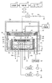
図1は、実施形態に係るエッチング装置の一例を示す縦断面図である。本実施形態におけるプラズマエッチング装置は、容量結合型平行平板プラズマエッチング装置として構成されており、例えば表面が陽極酸化処理されたアルミニウムからなる略円筒状のチャンバ(処理容器)10を有している。このチャンバ10は保安接地されている。
FIG. 1 is a longitudinal sectional view showing an example of an etching apparatus according to the embodiment. The plasma etching apparatus according to the present embodiment is configured as a capacitively coupled parallel plate plasma etching apparatus, and includes a substantially cylindrical chamber (processing vessel) 10 made of aluminum having an anodized surface. The
チャンバ10の底部には、セラミックス等からなる絶縁板12を介して円柱状のサセプタ支持台14が配置され、このサセプタ支持台14の上に例えばアルミニウムからなるサセプタ16が設けられている。サセプタ16は下部電極を構成し、その上に被処理基板である半導体ウエハWが載置される。この半導体ウエハWには本発明のエッチング対象である有機膜が形成されている。
A
サセプタ16の上面には、半導体ウエハWを静電力で吸着保持する静電チャック18が設けられている。この静電チャック18は、導電膜からなる電極20をAl2O3等の誘電体の絶縁層で挟んだ構造を有する。電極20には直流電源22が電気的に接続されている。そして、直流電源22からの直流電圧により生じたクーロン力等の静電力により半導体ウエハWが静電チャック18に吸着保持される。
On the upper surface of the susceptor 16, an
静電チャック18(半導体ウエハW)の周囲でサセプタ16の上面には、エッチングの均一性を向上させるための、例えばシリコンからなる導電性のフォーカスリング(補正リング)24が配置されている。サセプタ16およびサセプタ支持台14の側面には、例えば石英からなる円筒状の内壁部材26が設けられている。
A conductive focus ring (correction ring) 24 made of, for example, silicon is disposed on the upper surface of the susceptor 16 around the electrostatic chuck 18 (semiconductor wafer W) to improve etching uniformity. A cylindrical
サセプタ支持台14の内部には、例えば円周上に冷媒室28が設けられている。この冷媒室28には、外部に設けられた図示しないチラーユニットより配管30a,30bを介して所定温度の冷媒、例えば冷却水が循環供給され、冷媒の温度によってサセプタ16上の半導体ウエハWの処理温度を制御することができる。
Inside the susceptor support 14, for example, a
更に、図示しない伝熱ガス供給機構からの冷熱伝達用ガス(冷却ガス)、例えばHeガスがガス供給ライン32を介して静電チャック18の上面と半導体ウエハWの裏面との間に供給される。これらの構成によって、半導体ウエハWを、所定の温度に制御可能となっている。
Further, a cold transfer gas (cooling gas), for example, He gas from a heat transfer gas supply mechanism (not shown) is supplied between the upper surface of the
下部電極であるサセプタ16の上方には、サセプタ16と対向するように平行に上部電極34が設けられている。そして、上部電極34および下部電極16間の空間にプラズマが生成される。
Above the susceptor 16 that is the lower electrode, an
この上部電極34は、絶縁性遮蔽部材42を介して、チャンバ10の上部に支持されており、サセプタ16との対向面を構成しかつ多数のガス吐出孔37を有する。また、上部電極34は、導電性材料、例えばアルミニウムからなる水冷構造の電極支持体38を有する。電極支持体38の内部には、ガス拡散室40が設けられ、このガス拡散室40からはガス吐出孔37に連通する多数のガス通流孔41が下方に延びている。
The
電極支持体38にはガス拡散室40へ処理ガスを導くガス導入口62が形成されており、このガス導入口62にはガス供給管64が接続され、ガス供給管64には処理に必要なガスを供給するガス供給源66が接続されている。ガス供給管64には、複数のガス配管が接続されており、これらガス配管には流量制御器および開閉バルブ(いずれも図示せず)が設けられている。そして、処理に必要なガスは、ガス供給源66からガス供給管64を介してガス拡散室40に至り、ガス通流孔41およびガス吐出孔37を介してシャワー状にプラズマ生成空間に吐出される。すなわち、上部電極34は処理ガスを供給するためのシャワーヘッドとして機能する。
The
上部電極34には、ローパスフィルタ(LPF)51を介して可変直流電源50が電気的に接続されている。可変直流電源50は、負極が上部電極34側となるように接続されており、上部電極34にマイナスの電圧を印加するようになっている。可変直流電源50からの給電はオン・オフスイッチ52によりオン・オフが可能となっている。ローパスフィルタ(LPF)51は後述する第1および第2の高周波電源からの高周波をトラップするものであり、好適にはLRフィルタまたはLCフィルタで構成される。
A variable
チャンバ10の側壁から上部電極34の高さ位置よりも上方に延びるように円筒状の接地導体10aが設けられている。
A
下部電極であるサセプタ16には、第1の整合器46を介して、第1の高周波電源48が電気的に接続されている。第1の高周波電源48は、27〜100MHzの周波数、例えば60MHzの高周波電力を出力する。第1の整合器46は、第1の高周波電源48の内部(または出力)インピーダンスに負荷インピーダンスを整合させるもので、チャンバ10内にプラズマが生成されている時に第1の高周波電源48の出力インピーダンスと負荷インピーダンスが見かけ上一致するように機能する。
A first high
また、下部電極であるサセプタ16には、第2の整合器88を介して第2の高周波電源90も電気的に接続されている。この第2の高周波電源90から下部電極であるサセプタ16に高周波電力が供給されることにより、半導体ウエハWに高周波バイアスが印加され半導体ウエハWにイオンが引き込まれる。第2の高周波電源90は、400kHz〜20MHzの範囲内の周波数、例えば13.56MHzの高周波電力を出力する。第2の整合器88は第2の高周波電源90の内部(または出力)インピーダンスに負荷インピーダンスを整合させるためのもので、チャンバ10内にプラズマが生成されている時に第2の高周波電源90の内部インピーダンスとチャンバ10内のプラズマを含めた負荷インピーダンスが見かけ上一致するように機能する。
In addition, a second high
チャンバ10の底部には排気口80が設けられ、この排気口80に排気管82を介して排気装置84が接続されている。排気装置84は、ターボ分子ポンプなどの真空ポンプを有しており、チャンバ10内を所望の真空度まで減圧可能となっている。また、チャンバ10の側壁には半導体ウエハWの搬入出口85が設けられており、この搬入出口85はゲートバルブ86により開閉可能となっている。また、チャンバ10の内壁に沿ってチャンバ10にエッチング副生物(デポ)が付着することを防止するためのデポシールド11が着脱自在に設けられている。すなわち、デポシールド11がチャンバ壁を構成している。また、デポシールド11は、内壁部材26の外周にも設けられている。チャンバ10の底部のチャンバ壁側のデポシールド11と内壁部材26側のデポシールド11との間には排気プレート83が設けられている。デポシールド11および排気プレート83としては、アルミニウム材にY2O3等のセラミックスを被覆したものを好適に用いることができる。
An
デポシールド11のチャンバ内壁を構成する部分の半導体ウエハWとほぼ同じ高さの部分には、グランドにDC的に接続された導電性部材(GNDブロック)91が設けられており、これにより異常放電防止効果を発揮する。なお、この導電性部材91は、プラズマ生成領域に設けられていれば、その位置は図1の位置に限定されず、例えばサセプタ16の周囲に設ける等、サセプタ16側に設けてもよく、また上部電極34の外側にリング状に設ける等、上部電極34近傍に設けてもよい。
A conductive member (GND block) 91 connected to the ground in a DC manner is provided at a portion of the
プラズマエッチング装置の各構成部、例えば電源系やガス供給系、駆動系、更には、第1の高周波電源48、第2の高周波電源90、整合器46,88等は、マイクロプロセッサ(コンピュータ)を含む制御部(全体制御装置)100に接続されて制御される構成となっている。また、制御部100には、オペレータがプラズマエッチング装置を管理するためにコマンドの入力操作等を行うキーボードや、プラズマエッチング装置の稼働状況を可視化して表示するディスプレイ等からなるユーザーインターフェース101が接続されている。
Each component of the plasma etching apparatus, for example, a power supply system, a gas supply system, a drive system, a first high-
更に、制御部100には、プラズマエッチング装置で実行される各種処理を制御部100で実現するための制御プログラムや、処理条件に応じてプラズマエッチング装置の各構成部に処理を実行させるためのプログラムすなわち処理レシピが格納された記憶部102が接続されている。処理レシピは記憶部102の中の記憶媒体に記憶されている。記憶媒体は、ハードディスクや半導体メモリであってもよいし、CDROM、DVD、フラッシュメモリ等の可搬性のものであってもよい。また、他の装置から、例えば専用回線を介してレシピを適宜伝送させるようにしてもよい。
Further, the
そして、必要に応じて、ユーザーインターフェース101からの指示等にて任意の処理レシピを記憶部102から呼び出して制御部100にて実行させることで、プラズマエッチング装置での所望の処理が行われる。
Then, if necessary, an arbitrary processing recipe is called from the
例えば、制御部100は、後述するプラズマエッチング方法を実行するようにプラズマエッチング装置の各部を制御する。その一例を挙げて詳細な説明をする。制御部100は、マスク膜203上に形成された所定のパターンを有するフォトレジスト膜204をプラズマ処理するようにプラズマエッチング装置の各部を制御する。そして、制御部100は、プラズマ処理されたフォトレジスト膜204のパターンに沿ってマスク膜203をプラズマによりエッチングして、マスク膜203の下層に形成されている有機膜202を露出させるようにプラズマエッチング装置の各部を制御する。そして、制御部100は、O2、COS、およびCl2を含む混合ガスによるプラズマにより有機膜202をエッチングするようにプラズマエッチング装置の各部を制御する。
For example, the
図2は、実施形態に係るエッチング装置でエッチングされる半導体ウエハの構造の一例を説明するための模式図である。本実施形態では、一例として図2に示すような構造の半導体ウエハWを用いる。 FIG. 2 is a schematic diagram for explaining an example of a structure of a semiconductor wafer etched by the etching apparatus according to the embodiment. In the present embodiment, a semiconductor wafer W having a structure as shown in FIG. 2 is used as an example.
ここで用いる半導体ウエハWは、図2に示すように、基板上に下層膜201、有機膜202、マスク膜(無機膜)203、BARC(有機膜)およびフォトレジスト(PR)膜204を順次形成した後、フォトレジスト膜204にフォトリソグラフィにより所定パターンを形成した構造を有している。
As shown in FIG. 2, the semiconductor wafer W used here sequentially forms a
本実施形態におけるエッチング対象膜である有機膜202としては、通常この分野で用いられる有機膜であって、シリコンが含まれていないものであれば制限はなく、アモルファスカーボン(a−C)やSOC(スピンオンカーボン)、SOH(スピンオンハードマスク)等を好適に用いることができる。有機膜202の厚さは100〜1000nm程度で、例えば200nmである。
The
マスク膜203としては、例えばSiON膜(シリコン酸窒化膜)を好適に用いることができ、その厚さは10〜100nm程度で、例えばそれぞれ12nmおよびと20nmである。フォトレジスト膜204は、典型的にはArF(フッ化アルゴン)レジストであり、その厚さは20〜200nm程度である。
The
次に、本実施形態に係るプラズマエッチングの原理について図3を用いて説明する。図3は、処理ガスと溝の形状との関係の一例を示す模式図である。図3(a)は、処理ガスにCOSもCl2も含まれていないCF系の処理ガスのプラズマによりマスク膜203をマスクとして有機膜202をエッチングした場合の溝の形状の一例を示す模式図である。図3(a)に示すように、有機膜202に形成された溝の形状は、溝の開口や底の幅に比べて溝の中央が膨らむ形状となるボーイングが生成される。そのため、溝を設計値通りの幅にするためには、ボーイングによる中央部分の膨らみを考慮して、マスク膜をエッチングするBT工程においてマスク膜203に開けられる溝の幅を狭くすることにより、有機膜202の溝の開口を狭くする必要がある。
Next, the principle of plasma etching according to the present embodiment will be described with reference to FIG. FIG. 3 is a schematic diagram showing an example of the relationship between the processing gas and the groove shape. FIG. 3A is a schematic diagram showing an example of the shape of the groove when the
しかし、マスク膜203の溝の幅を、高い精度を保ちながら狭くすることには高度な微細化の技術を必要とする。また、開口の狭い溝をエッチングにより有機膜202に形成できたとしても、溝の内部に比べて開口が狭いため、その後の工程において、内部に溜まった堆積物を除去したり、有機膜202に形成された溝の内壁に均一な膜を形成すること等が難しくなる場合がある。
However, in order to reduce the width of the groove of the
ここで、溝の開口の幅が溝の底の幅よりも広くなるように溝の内壁に傾斜(テーパ)が形成できれば、半導体の製造工程において内部に溜まった堆積物を除去したり、溝の内壁に均一な膜を形成すること等が容易になる。ただし、高密度化を達成するためには、溝の内壁の傾斜を緩やかにし過ぎることもできない。これらを考慮すると、テーパの角度は、84°〜89°であることが好ましい。より好ましくは、テーパの角度は、84°〜86°であるとよい。 Here, if the inner wall of the groove can be inclined (tapered) so that the width of the groove opening is wider than the width of the groove bottom, deposits accumulated inside the semiconductor manufacturing process can be removed, It becomes easy to form a uniform film on the inner wall. However, in order to achieve high density, the inclination of the inner wall of the groove cannot be made too gentle. Considering these, the taper angle is preferably 84 ° to 89 °. More preferably, the taper angle is 84 ° to 86 °.
また、ボーイングの発生を抑える添加ガスとしては、COSガスが知られている。図3(b)は、処理ガスにCOSガスを添加、又はCOS単ガスの処理ガスのプラズマによりマスク膜203をマスクとして有機膜202をエッチングした場合の溝の形状の一例を示す模式図である。図3(b)に示すように、処理ガスにCOSガスが添加されると、プラズマ中に生成されたS(硫黄)成分のイオンにより、溝の内壁にSの堆積物が付着しながらエッチングされるので、ボーイングの発生がある程度抑えられる。しかし、COSガスを用いることでボーイングが抑制されたとしても、不十分であり、且つテーパ形状が形成されない。そのため、依然としてボーイングの抑制及びテーパ形状を考慮した設計が必要となる。
Further, COS gas is known as an additive gas that suppresses the occurrence of bowing. FIG. 3B is a schematic diagram showing an example of the shape of the groove when the COS gas is added to the processing gas or the
図3(c)は、処理ガスにCl2ガスを添加、又はCl2単ガスの処理ガスのプラズマによりマスク膜203をマスクとして有機膜202をエッチングした場合の溝の形状の一例を示す模式図である。図3(c)に示すように、COSガスを用いた場合と同様に、処理ガスにCl2ガスが添加されると、プラズマ中に生成されたSiClx(塩化ケイ素)成分のイオンにより、溝の内壁にSiClxの堆積物が付着しながらエッチングされるので、ボーイングの発生がある程度抑えられる。しかし、Cl2ガスを用いることでボーイングが抑制されたとしても、不十分であり、且つテーパ形状が形成されない。そのため、依然としてボーイングの抑制及びテーパ形状を考慮した設計が必要となる。
FIG. 3C is a schematic diagram showing an example of the shape of the groove when the
そこで、本実施形態の有機膜エッチング工程では、O2ガス/Cl2ガス/COSガスを含む処理ガスのプラズマにより有機膜202をエッチングする。図3(d)は、O2ガス/Cl2ガス/COSガスを含む処理ガスのプラズマによりマスク膜203をマスクとして有機膜202をエッチングした場合の溝の形状の一例を示す模式図である。
Therefore, in the organic film etching process of the present embodiment, the
発明者は、鋭意研究の結果、処理ガスにCOSガスおよびCl2ガスが添加されると、図3(d)に示すように、プラズマ中に生成されたS成分のイオンおよびSiClx成分のイオンにより、溝の内壁にSとSiClxの混合堆積物が付着しながらエッチングされるので、ボーイングの発生が大幅に抑えられることが分かった。これにより、溝の内壁をテーパ形状とすることができ、後の工程において溝の内部に溜まった堆積物の除去や、溝の内壁に均一な膜を形成すること等が容易になる。このように、本願発明のエッチング方法により有機膜をエッチングして、好ましいCDやテーパ形状の溝を形成した後、その有機膜202をマスクとして、例えばSiON膜、TiN(メタルハードマスク)等の下層膜201をプラズマによりエッチングすることにより、下層膜201に形成される溝のCD及び形状を高い精度で形成することが可能となる。さらに、その下層膜の下層に形成する膜を、下層膜をマスクとしてエッチングすることで、良好な形状の溝を形成することが可能となる。また、これにより、半導体装置の性能及び歩留まりを向上させることが可能となる。
As a result of earnest research, the inventor, when COS gas and Cl2 gas are added to the processing gas, as shown in FIG. 3 (d), due to ions of S component and SiClx component generated in the plasma, It was found that since the mixed deposit of S and SiClx adheres to the inner wall of the groove and is etched, the occurrence of bowing is greatly suppressed. As a result, the inner wall of the groove can be tapered, and it becomes easy to remove deposits accumulated in the groove in a subsequent process, to form a uniform film on the inner wall of the groove, and the like. Thus, by etching grayed organic film by the etching method of the present invention, after forming the grooves in the preferred CD or tapered, and the
<プラズマエッチング方法の実施形態>
次に、本実施形態におけるプラズマエッチング方法の各工程について説明する。図4は、本実施形態に係るプラズマエッチング方法の手順の一例を示すフローチャートである。
<Embodiment of Plasma Etching Method>
Next, each step of the plasma etching method in the present embodiment will be described. FIG. 4 is a flowchart showing an example of the procedure of the plasma etching method according to the present embodiment.
本実施形態におけるプラズマエッチング方法では、図4に示すように、まず、被処理体となる半導体ウエハWがチャンバ10内に搬入されてサセプタ16上に載置され。そして、制御部100は、排気装置84の真空ポンプにより排気口80を介してチャンバ10内を所定の圧力まで排気し、チャンバ10内に処理ガスを供給してプラズマ処理を実行する(ステップS100)。
In the plasma etching method according to the present embodiment, as shown in FIG. 4, first, a semiconductor wafer W to be processed is loaded into the
例えば、制御部100は、水素を含む処理ガスをガス供給源66からチャンバ10内に供給し、水素含有ガスのプラズマによりフォトレジスト膜の表面をプラズマ処理してレジスト膜を固化させる。プラズマ処理工程は、キュア工程とも称され、マスクとして用いられるフォトレジスト膜のSWR(Side Wall Roughness)やLER(Line Edge Roughness)等を改善する。
For example, the
より詳細には、制御部100は、例えば、以下の条件でフォトレジスト膜204をプラズマ処理を実行する。
チャンバ10内の圧力:10mT
上部電極34に供給する高周波電力:200W
上部電極34に供給する電力の周波数:60MHz
下部電極(サセプタ16)に供給する高周波電力:0W
供給ガスおよび流量比:H2(水素)/N2(窒素)/CH4(メタン)=180/60/10sccm
冷却ガスの圧力:20/20Torr
上部電極34の温度:90℃
チャンバ10の内壁の温度:60℃
サセプタ16の中央の温度:15℃
サセプタ16のエッジの温度:5℃
More specifically, the
Pressure in chamber 10: 10 mT
High frequency power supplied to the upper electrode 34: 200 W
Frequency of power supplied to the upper electrode 34: 60 MHz
High frequency power supplied to the lower electrode (susceptor 16): 0W
Supply gas and flow ratio: H2 (hydrogen) / N2 (nitrogen) / CH4 (methane) = 180/60/10 sccm
Cooling gas pressure: 20/20 Torr
Temperature of upper electrode 34: 90 ° C
Temperature of inner wall of chamber 10: 60 ° C
Central temperature of susceptor 16: 15 ° C
Edge temperature of susceptor 16: 5 ° C
次に、制御部100は、チャンバ10内を排気し、チャンバ10内に処理ガスを供給して、マスク膜203のエッチング工程を実行する(ステップS101)。例えば、制御部100は、CF系ガス及びCH系ガスを含む処理ガスをガス供給源66からチャンバ10内に供給し、プラズマ処理されたフォトレジスト膜204をマスクとしてCF系ガス及びCH系含有ガスによるプラズマによりBARC(有機膜)及びシリコン含有膜であるマスク膜203をエッチングして、マスク膜203の下層に形成されている、Siを含まない有機膜202を露出させる。マスク膜203のエッチング工程は、BT(Break Through)工程とも称される。この場合、マスク膜203上には、ArF等のフォトレジスト膜204が所定の厚みで残される。
Next, the
より詳細には、制御部100は、例えば、以下の条件でマスク膜203のエッチングを行う。
チャンバ10内の圧力:15mT
上部電極34に供給する高周波電力:500W
上部電極34に供給する電力の周波数:60MHz
下部電極(サセプタ16)に供給する高周波電力:100W
下部電極(サセプタ16)に供給する電力の周波数:13MHz
供給ガスおよび流量比:CF4(四フッ化炭素)/CH4/O2=250/20/8sccm
冷却ガスの圧力:20/20Torr
上部電極34の温度:90℃
チャンバ10の内壁の温度:60℃
サセプタ16の中央の温度:15℃
サセプタ16のエッジの温度:5℃
More specifically, for example, the
Pressure in chamber 10: 15 mT
High frequency power supplied to the upper electrode 34: 500 W
Frequency of power supplied to the upper electrode 34: 60 MHz
High frequency power supplied to the lower electrode (susceptor 16): 100W
Frequency of power supplied to the lower electrode (susceptor 16): 13 MHz
Supply gas and flow rate ratio: CF4 (carbon tetrafluoride) / CH4 / O2 = 250/20/8 sccm
Cooling gas pressure: 20/20 Torr
Temperature of upper electrode 34: 90 ° C
Temperature of inner wall of chamber 10: 60 ° C
Central temperature of susceptor 16: 15 ° C
Edge temperature of susceptor 16: 5 ° C
次に、制御部100は、チャンバ10内を排気し、チャンバ10内に処理ガスを供給して、Siを含まない有機膜202のエッチング工程を実行する(ステップS102)。例えば、制御部100は、COSおよびCl2を含む処理ガスをガス供給源66からチャンバ10内に供給し、残膜のフォトレジスト膜204およびマスク膜203をマスクとして、COSガスおよびCl2ガス含有ガスのプラズマにより、Siを含まない有機膜202をエッチングする。
Next, the
より詳細には、制御部100は、例えば、以下の条件で、Siを含まない有機膜202のエッチングを行う。
チャンバ10内の圧力:10mT
上部電極34に供給する高周波電力:500W
上部電極34に供給する電力の周波数:60MHz
下部電極(サセプタ16)に供給する高周波電力:200W
下部電極(サセプタ16)に供給する電力の周波数:13.56MHz
供給ガス:O2/He(ヘリウム)/Cl2/COS
冷却ガスの圧力:20/20Torr
上部電極34の温度:90℃
チャンバ10の内壁の温度:60℃
サセプタ16の中央の温度:15℃
サセプタ16のエッジの温度:5℃
More specifically, the
Pressure in chamber 10: 10 mT
High frequency power supplied to the upper electrode 34: 500 W
Frequency of power supplied to the upper electrode 34: 60 MHz
High frequency power supplied to the lower electrode (susceptor 16): 200W
Frequency of power supplied to the lower electrode (susceptor 16): 13.56 MHz
Supply gas: O2 / He (helium) / Cl2 / COS
Cooling gas pressure: 20/20 Torr
Temperature of upper electrode 34: 90 ° C
Temperature of inner wall of chamber 10: 60 ° C
Central temperature of susceptor 16: 15 ° C
Edge temperature of susceptor 16: 5 ° C
なお、Siを含まない有機膜202のエッチング工程においてチャンバ10内に供給される処理ガスにはO2およびHeが多く含まれているため、プラズマが発生しにくい。そのため、制御部100は、チャンバ10内の圧力を一時的に20mTまで上げてからプラズマを発生させ、プラズマが安定的に発生した後に、チャンバ10内の圧力を処理圧力である10mTまで下げる制御を行うことが好ましい。
Note that in the etching process of the
<実施例1>
次に、図2に示した膜構成の半導体ウエハWを用いて、COSガスおよびCl2ガスの流量を変えてエッチングし、流量比と、CDおよびテーパ角度との関係を調べる実験を行った。以下の実験結果では、マスク膜203/有機膜202/下層膜201=28/170/40nmの半導体ウエハWを用いている。また、プロセス条件は、以下の3通りである。
供給ガス:O2/He/Cl2/COS=50/160/20/8sccm ・・・(1)
=50/160/13/6sccm ・・・(2)
=50/160/16/8sccm ・・・(3)
各ガスの好ましい流量は、COSガスでは3〜10sccm、Cl2ガスでは10〜25sccm、Heガスでは100〜200sccm、O2ガスでは45〜100sccmである。その他のステップ及び条件は、前述の有機膜エッチングの条件と同様である。
<Example 1>
Next, using the semiconductor wafer W having the film configuration shown in FIG. 2, etching was performed while changing the flow rates of the COS gas and the
Supply gas: O2 / He / Cl2 / COS = 50/160/20/8 sccm (1)
= 50/160/13/6 sccm (2)
= 50/160/16 / 8sccm (3)
The preferred flow rates of each gas are 3 to 10 sccm for COS gas, 10 to 25 sccm for
図5(a)〜(c)は、COSガスおよびCl2ガスを含む処理ガスのプラズマによりエッチングした場合の溝の断面の実験結果の一例を示す。図5(a)は、上記(1)で示した流量比の処理ガスを用いてエッチングした場合の溝の断面を示し、図5(b)は、上記(2)で示した流量比の処理ガスを用いてエッチングした場合の溝の断面を示し、図5(c)は、上記(3)で示した流量比の処理ガスを用いてエッチングした場合の溝の断面を示す。
FIGS. 5A to 5C show an example of experimental results of the cross section of the groove when etching is performed with plasma of a processing gas containing COS gas and
上記(1)で示した流量比の処理ガスを用いてエッチングした場合には、図5(a)に示すように、溝の開口の幅が、溝の底の幅よりも広くなっており、溝の側壁の傾斜も妥当な範囲に含まれている。図5(a)の場合、溝の開口の幅は271nm、溝の底の幅は239nmであった。なお、上記(1)に示した流量比の処理ガスでは、Cl2ガスの流量に対するCOSガスの流量の比は、0.4である。
When etching is performed using the process gas having the flow ratio shown in (1) above, the width of the groove opening is wider than the width of the groove bottom, as shown in FIG. The inclination of the side wall of the groove is also included in a reasonable range. In the case of FIG. 5A, the width of the groove opening was 271 nm, and the width of the groove bottom was 239 nm. In the processing gas having the flow ratio shown in (1) above, the ratio of the flow rate of COS gas to the flow rate of
また、上記(2)で示した流量比の処理ガスを用いてエッチングした場合も、図5(b)に示すように、溝の開口の幅が、溝の底の幅よりも広くなっており、溝の側壁にテーパが形成されている。図5(b)の場合、溝の開口の幅は264nm、溝の底の幅は257nmであった。なお、上記(2)に示した流量比の処理ガスでは、Cl2の流量に対するCOSの流量の比は、0.46である。
Also, when etching is performed using the processing gas having the flow rate ratio shown in (2) above, the width of the groove opening is wider than the width of the groove bottom as shown in FIG. The taper is formed on the side wall of the groove. In the case of FIG. 5B, the width of the groove opening was 264 nm, and the width of the groove bottom was 257 nm. In the processing gas having the flow rate ratio shown in (2) above, the ratio of the COS flow rate to the
また、上記(3)で示した流量比の処理ガスを用いてエッチングした場合も、図5(c)に示すように、溝の開口の幅が、溝の底の幅よりも広くなっており、溝の側壁にテーパが形成されている。図5(c)の場合、溝の開口の幅は270nm、溝の底の幅は255nmであった。なお、上記(3)に示した流量比の処理ガスでは、Cl2の流量に対するCOSの流量の比は、0.5である。
Also, when etching is performed using the processing gas having the flow ratio shown in (3) above, the width of the groove opening is wider than the width of the groove bottom, as shown in FIG. The taper is formed on the side wall of the groove. In the case of FIG. 5C, the width of the groove opening was 270 nm, and the width of the groove bottom was 255 nm. In the processing gas having the flow ratio shown in (3) above, the ratio of the COS flow rate to the
ここで、本明細書では、例えば図6に示すような角度θをテーパ角度と定義する。テーパ角度θは、溝の開口の幅をTopCDとし、溝の底の幅をBottomCDとし、溝の深さ(有機膜202の厚み)をLとして、例えば、下記の算出式(4)を用いて算出される。
θ=tan-1{L/((TopCD−BottomCD)/2)} ・・・(4)
Here, in this specification, for example, an angle θ as shown in FIG. 6 is defined as a taper angle. For the taper angle θ, the width of the opening of the groove is TopCD, the width of the bottom of the groove is BottomCD, the depth of the groove (thickness of the organic film 202) is L, and the following calculation formula (4) is used. Calculated.
θ = tan −1 {L / ((TopCD-BottomCD) / 2)} (4)
上記(1)〜(3)で示した流量比の処理ガスを用いてエッチングした場合のそれぞれの溝の形状において、TopCDとBottomCDとからテーパ角度を算出すると、例えば図7に示すようになる。また、テーパ角度の計算結果をプロットすると、例えば図8に示すようなグラフになる。図7は、COSガスとCl2ガスの流量の比に対するテーパ角度の計算結果の一例を示す。図8は、COSガスとCl2ガスの流量の比に対するテーパ角度の変化の一例を示すグラフである。
When the taper angle is calculated from TopCD and BottomCD in the shape of each groove in the case of etching using the processing gas having the flow ratio shown in the above (1) to (3), for example, as shown in FIG. Further, when the calculation result of the taper angle is plotted, for example, a graph as shown in FIG. 8 is obtained. FIG. 7 shows an example of the calculation result of the taper angle with respect to the ratio of the flow rates of COS gas and
図7および図8からわかるように、Cl2ガスの流量に対するCOSガスの流量の比が増加するに従って、テーパ角度が増加する傾向がみられる。テーパ角度は、84°〜89°の範囲内となることが好ましい。図7および図8の結果を参照すると、Cl2ガスの流量に対するCOSガスの流量の比が0.4〜0.5の範囲であれば、テーパ角度が、ボーイングを抑制しつつ、好ましいテーパ角度の84°〜89°の範囲内になっていることがわかる。
As can be seen from FIGS. 7 and 8, the taper angle tends to increase as the ratio of the flow rate of COS gas to the flow rate of
また、発明者は、更に鋭意研究を重ねた結果、Cl2ガスの流量に対するCOSガスの流量の比が0.35〜0.5の範囲であれば、テーパ角度が、ボーイングを抑制しつつ、好ましいテーパ角度の84°〜89°の範囲に含まれることが分かった。そのため、処理ガスに含まれるCOSガスとCl2ガスの流量比は、Cl2ガスの流量に対するCOSガスの流量の比が0.35〜0.5の範囲内であることが好ましい。
In addition, as a result of further earnest research, the inventor is preferable that the ratio of the flow rate of the COS gas to the flow rate of the Cl2 gas is in the range of 0.35 to 0.5, while suppressing the bowing. It was found that the taper angle was included in the range of 84 ° to 89 °. Therefore, the flow rate ratio between the COS gas and the
また、テーパ角度の範囲は、より好ましくは、84°〜86°の範囲であるとよい。ここで、図7および図8の結果を参照すると、Cl2ガスの流量に対するCOSガスの流量の比が0.4であれば、テーパ角度が、ボーイングを抑制しつつ、好ましいテーパ角度の84°〜86°の範囲内になっていることがわかる。また、発明者は、更に鋭意研究を重ねた結果、Cl2ガスの流量に対するCOSガスの流量の比が0.35〜0.45の範囲であれば、テーパ角度が、ボーイングを抑制しつつ、好ましいテーパ角度の84°〜86°の範囲に含まれることが分かった。そのため、処理ガスに含まれるCOSガスとCl2ガスの流量比は、Cl2ガスの流量に対するCOSガスの流量の比が0.35〜0.45の範囲であることが更に好ましい。
The taper angle range is more preferably 84 ° to 86 °. Here, referring to the results of FIG. 7 and FIG. 8, if the ratio of the flow rate of the COS gas to the flow rate of the Cl2 gas is 0.4, the taper angle is 84 ° to a preferable taper angle while suppressing bowing. It turns out that it is in the range of 86 degrees. Further, as a result of further earnest research, the inventor is preferable that the ratio of the flow rate of the COS gas to the flow rate of the Cl2 gas is in the range of 0.35 to 0.45, while suppressing the bowing. It was found that the taper angle was included in the range of 84 ° to 86 °. Therefore, it is more preferable that the flow rate ratio between the COS gas and the
<実施例2>
次に、図2に示した膜構成の半導体ウエハWを用いて、COSガスおよびCl2ガスに対してO2ガスの流量を変えてエッチングし、流量比と、CDおよびテーパ角度との関係を調べる実験を行った。以下の実験におけるプロセス条件は、以下の3通りである。
供給ガス:O2/He/Cl2/COS=40/160/20/8sccm ・・・(5)
=50/160/20/8sccm ・・・(6)
=70/160/20/8sccm ・・・(7)
各ガスの好ましい流量は、COSガスでは3〜10sccm、Cl2ガスでは10〜25sccm、Heガスでは100〜200sccm、O2ガスでは45〜100sccmである。その他のステップ及び条件は、実施例1における有機膜エッチングの条件と同様である。
<Example 2>
Next, using the semiconductor wafer W having the film configuration shown in FIG. 2, the etching is performed by changing the flow rate of
Supply gas: O2 / He / Cl2 / COS = 40/160/20/8 sccm (5)
= 50/160/20 / 8sccm (6)
= 70/160/20 / 8sccm (7)
The preferred flow rates of each gas are 3 to 10 sccm for COS gas, 10 to 25 sccm for
図9(a)〜(c)は、COSガス、Cl2ガス、およびO2ガスを含む処理ガスを用いてエッチングした場合の溝の断面の実験結果の一例を示す。図9(a)は、上記(5)で示した流量比の処理ガスを用いてエッチングした場合の溝の断面を示し、図9(b)は、上記(6)で示した流量比の処理ガスを用いてエッチングした場合の溝の断面を示し、図9(c)は、上記(7)で示した流量比の処理ガスを用いてエッチングした場合の溝の断面を示す。
FIGS. 9A to 9C show an example of experimental results of groove cross sections when etching is performed using a processing gas containing COS gas,
上記(5)で示した流量比の処理ガスを用いてエッチングした場合には、図9(a)に示すように、溝の開口の幅が、溝の底の幅よりも広くなり過ぎており、溝の側壁の傾斜も小さくなり過ぎている。図9(a)の場合、溝の開口の幅は381nm、溝の底の幅は250nmであった。この場合、溝の底の幅(BottomCD)に対する溝の開口の幅(TopCD)の比であるCD比は、1.52である。また、上記(5)に示した流量比の処理ガスでは、COSガスの流量とCl2ガスの流量の合計に対するO2ガスの流量の比は、1.43である。 When etching is performed using the processing gas having the flow ratio shown in (5) above, the width of the groove opening is too wider than the width of the groove bottom, as shown in FIG. The inclination of the side wall of the groove is too small. In the case of FIG. 9A, the width of the groove opening was 381 nm, and the width of the groove bottom was 250 nm. In this case, the CD ratio, which is the ratio of the groove opening width (TopCD) to the groove bottom width (BottomCD), is 1.52. In the processing gas having the flow ratio shown in (5) above, the ratio of the flow rate of O2 gas to the total of the flow rate of COS gas and the flow rate of Cl2 gas is 1.43.
また、上記(6)で示した流量比の処理ガスを用いてエッチングした場合には、図9(b)に示すように、溝の開口の幅が、溝の底の幅よりも広くなっているものの、溝の側壁の傾斜は妥当な範囲に含まれている。図9(b)の場合、溝の開口の幅は271nm、溝の底の幅は239nmであった。この場合、CD比は、1.13である。また、上記(6)に示した流量比の処理ガスでは、COSガスの流量とCl2ガスの流量の合計に対するO2ガスの流量の比は、1.78である。
Further, when etching is performed using the processing gas having the flow ratio shown in (6) above, the width of the groove opening becomes wider than the width of the groove bottom, as shown in FIG. 9B. However, the inclination of the sidewall of the groove is within a reasonable range. In the case of FIG. 9B, the width of the groove opening was 271 nm and the width of the groove bottom was 239 nm. In this case, the CD ratio is 1.13. In the processing gas having the flow ratio shown in (6) above, the ratio of the flow rate of
また、上記(7)で示した流量比の処理ガスを用いてエッチングした場合には、図9(c)に示すように、溝の開口の幅が、溝の底の幅よりも広くなっているものの、溝の側壁のテーパの角度が急峻になっている。図9(c)の場合、溝の開口の幅は279nm、溝の底の幅は265nmであった。この場合、CD比は、1.05である。また、上記(7)に示した流量比の処理ガスでは、COSガスの流量とCl2ガスの流量の合計に対するO2ガスの流量の比は、2.5である。 When etching is performed using the processing gas having the flow ratio shown in (7) above, the width of the groove opening is wider than the width of the groove bottom, as shown in FIG. 9C. However, the taper angle of the side wall of the groove is steep. In the case of FIG. 9C, the width of the groove opening was 279 nm, and the width of the groove bottom was 265 nm. In this case, the CD ratio is 1.05. Further, the processing gas flow ratio shown in the above (7), the flow rate ratio of O2 gas to the total flow rate of the CO S gas flow and Cl2 gas is 2.5.
上記(5)〜(7)で示した流量比の処理ガスを用いてエッチングした場合のそれぞれの溝の形状において、TopCDとBottomCDとからCD比およびテーパ角度を算出すると、例えば図10に示すようになる。また、CD比およびテーパ角度の計算結果をプロットすると、例えば図11に示すようなグラフになる。図10は、COSガスの流量とCl2ガスの流量の合計に対するO2ガスの流量の比に対するCD比およびテーパ角度の計算結果の一例を示す。図11は、COSガスの流量とCl2ガスの流量の合計に対するO2ガスの流量の比に対するCD比およびテーパ角度の変化の一例を示すグラフである。
When the CD ratio and the taper angle are calculated from TopCD and BottomCD in the shape of each groove when etching is performed using the processing gas having the flow ratio shown in (5) to (7) above, for example, as shown in FIG. become. When the calculation results of the CD ratio and the taper angle are plotted, for example, a graph as shown in FIG. 11 is obtained. FIG. 10 shows an example of the calculation result of the CD ratio and the taper angle with respect to the ratio of the flow rate of
図10および図11の実験結果を参照すると、COSガスの流量とCl2ガスの流量の合計に対するO2ガスの流量の比を増加させると、CD比は減少する一方、テーパ角度は増加する傾向にあることがわかる。 Referring to the experimental results of FIGS. 10 and 11, when the ratio of the flow rate of O2 gas to the total flow rate of COS gas and Cl2 gas is increased, the CD ratio is decreased, but the taper angle tends to increase. I understand that.
また、図10および図11の実験結果を参照すると、COSガスの流量とCl2ガスの流量の合計に対するO2ガスの流量の比が1.78〜2.63の範囲内が好ましい。その場合、テーパ角度が、好ましいテーパ角度の範囲である84°〜89°の範囲内の角度となっていることがわかる。 10 and 11, it is preferable that the ratio of the flow rate of O2 gas to the sum of the flow rate of COS gas and the flow rate of Cl2 gas is in the range of 1.78 to 2.63. In this case, it can be seen that the taper angle is an angle within the range of 84 ° to 89 ° which is a preferable taper angle range.
また、発明者は、更に鋭意研究を重ねた結果、Cl2の流量とCOSの流量の合計に対するO2の流量の比が1.5〜2.7の範囲であれば、テーパ角度が、好ましいテーパ角度の84°〜89°の範囲に含まれることが分かった。そのため、処理ガスにおいて、COSガスの流量とCl2ガスの流量の合計に対するO2ガスの流量の比は、1.5〜2.7の範囲内であることが好ましい。 Further, as a result of further intensive studies, the inventors have determined that if the ratio of the flow rate of O2 to the total flow rate of Cl2 and the flow rate of COS is in the range of 1.5 to 2.7, the taper angle is a preferable taper angle. Was found to fall within the range of 84 ° to 89 °. Therefore, in the processing gas, the ratio of the flow rate of O2 gas to the total flow rate of COS gas and Cl2 gas is preferably in the range of 1.5 to 2.7.
また、図10および図11の実験結果を参照すると、COSガスの流量とCl2ガスの流量の合計に対するO2ガスの流量の比が1.78である場合に、テーパ角度が、より好ましいテーパ角度の範囲である84°〜86°の範囲内の角度となっていることがわかる。 10 and 11, when the ratio of the flow rate of O2 gas to the total flow rate of COS gas and Cl2 gas is 1.78, the taper angle is a more preferable taper angle. It can be seen that the angle is within the range of 84 ° to 86 °.
また、発明者は、更に鋭意研究を重ねた結果、COSガスの流量とCl2ガスの流量の合計に対するO2ガスの流量の比が1.7〜1.9の範囲内であれば、テーパ角度が、より好ましいテーパ角度の84°〜86°の範囲内に含まれることが分かった。そのため、処理ガスにおいて、COSガスの流量とCl2ガスの流量の合計に対するO2ガスの流量の比は、1.7〜1.9の範囲内であることが更に好ましい。従って、ボーイングを抑制しつつ、好ましいテーパ角度の範囲内の溝を形成するガス条件として、COSガスの流量とCl2ガスの流量の合計に対するO2ガスの流量の比が1.5〜2.7の範囲内が好ましく、また、Cl2ガスの流量に対するCOSガスの流量の比が0.35〜0.5の範囲が好ましい。 Further, as a result of further earnest research, the inventor has determined that the taper angle is as long as the ratio of the O2 gas flow rate to the total of the COS gas flow rate and the Cl2 gas flow rate is within a range of 1.7 to 1.9. It was found that the taper angle was included in the range of 84 ° to 86 ° of the more preferable taper angle. Therefore, in the processing gas, it is more preferable that the ratio of the flow rate of O2 gas to the total flow rate of COS gas and Cl2 gas is in the range of 1.7 to 1.9. Therefore, as a gas condition for forming a groove within a preferable taper angle range while suppressing bowing, the ratio of the flow rate of O2 gas to the total flow rate of COS gas and Cl2 gas is 1.5 to 2.7. Within the range, the ratio of the flow rate of the COS gas to the flow rate of the Cl2 gas is preferably in the range of 0.35 to 0.5.
以上、本発明を実施の形態を用いて説明したが、本発明の技術的範囲は上記実施の形態に記載の範囲には限定されない。上記実施の形態に多様な変更または改良を加えることが可能であることが当業者には明らかである。また、そのような変更または改良を加えた形態も本発明の技術的範囲に含まれ得ることが、特許請求の範囲の記載から明らかである。 As mentioned above, although this invention was demonstrated using embodiment, the technical scope of this invention is not limited to the range as described in the said embodiment. It will be apparent to those skilled in the art that various modifications or improvements can be made to the above-described embodiment. In addition, it is apparent from the scope of the claims that the embodiments added with such changes or improvements can be included in the technical scope of the present invention.
10 チャンバ
16 サセプタ
34 上部電極
48 第1の高周波電源
50 可変直流電源
66 ガス供給源
90 第2の高周波電源
100 制御部
102 記憶部
W 半導体ウエハ
10 chamber 16
Claims (9)
前記レジスト膜は、所定のパターンを有し、前記レジスト膜をマスクとして前記マスク膜をエッチングしてマスクを形成し、
前記レジスト膜及びマスク膜をマスクとして、前記Siを含まない有機膜をO2(酸素)、COS(硫化カルボニル)、およびCl2(塩素)を含む混合ガスのプラズマによりエッチングすることを含み、
前記Cl2の流量に対する前記COSの流量の比は、0.35〜0.5の範囲であることを特徴とするプラズマエッチング方法。 On the substrate, an organic film not containing Si (silicon), a mask film, and a resist film are sequentially formed.
The resist film has a predetermined pattern, and the mask film is etched using the resist film as a mask to form a mask,
Etching the organic film not containing Si with a plasma of a mixed gas containing O2 (oxygen), COS (carbonyl sulfide), and Cl2 (chlorine) using the resist film and the mask film as a mask ,
The plasma etching method, wherein a ratio of the COS flow rate to the Cl 2 flow rate is in a range of 0.35 to 0.5 .
プラズマ処理された前記フォトレジスト膜のパターンに沿って前記マスク膜をプラズマによりエッチングして、前記マスク膜の下層に形成されている有機膜を露出させる第2の工程と、
O2(酸素)、COS(硫化カルボニル)、およびCl2(塩素)を含む混合ガスのプラズマにより前記有機膜をエッチングする第3の工程と
を含み、
前記Cl2の流量に対する前記COSの流量の比は、0.35〜0.5の範囲であることを特徴とするプラズマエッチング方法。 A first step of plasma processing a photoresist film having a predetermined pattern formed on the mask film;
A second step of exposing the organic film formed under the mask film by etching the mask film with plasma along a pattern of the photoresist film subjected to the plasma treatment;
A third step of etching the organic film by plasma of a mixed gas containing O2 (oxygen), COS (carbonyl sulfide), and Cl2 (chlorine) ,
The plasma etching method, wherein a ratio of the COS flow rate to the Cl 2 flow rate is in a range of 0.35 to 0.5 .
前記処理チャンバ内を減圧する減圧部と、
前記処理チャンバ内に処理ガスを供給するガス供給部と、
請求項1から8のいずれか一項に記載のプラズマエッチング方法を実行する制御部と
を備えることを特徴とするプラズマエッチング装置。 A processing chamber for performing a plasma etching process on an object to be processed;
A decompression section for decompressing the inside of the processing chamber;
A gas supply unit for supplying a processing gas into the processing chamber;
The plasma etching apparatus, characterized in that it comprises a control unit for performing a plasma etching method according to any one of claims 1 to 8.
Priority Applications (6)
| Application Number | Priority Date | Filing Date | Title |
|---|---|---|---|
| JP2013137118A JP6185305B2 (en) | 2013-06-28 | 2013-06-28 | Plasma etching method and plasma etching apparatus |
| EP14174609.9A EP2819151B1 (en) | 2013-06-28 | 2014-06-26 | Plasma etching method and plasma etching apparatus |
| US14/316,082 US9324569B2 (en) | 2013-06-28 | 2014-06-26 | Plasma etching method and plasma etching apparatus |
| TW103122141A TWI618145B (en) | 2013-06-28 | 2014-06-26 | Plasma etching method and plasma etching device |
| KR1020140079591A KR102245901B1 (en) | 2013-06-28 | 2014-06-27 | Plasma etching method and plasma etching apparatus |
| CN201410301711.2A CN104253036B (en) | 2013-06-28 | 2014-06-27 | Plasma-etching method and plasma-etching apparatus |
Applications Claiming Priority (1)
| Application Number | Priority Date | Filing Date | Title |
|---|---|---|---|
| JP2013137118A JP6185305B2 (en) | 2013-06-28 | 2013-06-28 | Plasma etching method and plasma etching apparatus |
Publications (3)
| Publication Number | Publication Date |
|---|---|
| JP2015012178A JP2015012178A (en) | 2015-01-19 |
| JP2015012178A5 JP2015012178A5 (en) | 2015-02-26 |
| JP6185305B2 true JP6185305B2 (en) | 2017-08-23 |
Family
ID=50981431
Family Applications (1)
| Application Number | Title | Priority Date | Filing Date |
|---|---|---|---|
| JP2013137118A Active JP6185305B2 (en) | 2013-06-28 | 2013-06-28 | Plasma etching method and plasma etching apparatus |
Country Status (6)
| Country | Link |
|---|---|
| US (1) | US9324569B2 (en) |
| EP (1) | EP2819151B1 (en) |
| JP (1) | JP6185305B2 (en) |
| KR (1) | KR102245901B1 (en) |
| CN (1) | CN104253036B (en) |
| TW (1) | TWI618145B (en) |
Families Citing this family (15)
| Publication number | Priority date | Publication date | Assignee | Title |
|---|---|---|---|---|
| JP6817692B2 (en) * | 2015-08-27 | 2021-01-20 | 東京エレクトロン株式会社 | Plasma processing method |
| JP6748354B2 (en) | 2015-09-18 | 2020-09-02 | セントラル硝子株式会社 | Dry etching method and dry etching agent |
| KR102535484B1 (en) * | 2016-11-29 | 2023-05-22 | 램 리써치 코포레이션 | Method for Creating Vertical Profiles in Etching an Organic Layer |
| JP6833657B2 (en) * | 2017-11-07 | 2021-02-24 | 東京エレクトロン株式会社 | How to plasma etch the substrate |
| CN108550578B (en) * | 2018-03-26 | 2020-10-02 | 长江存储科技有限责任公司 | Three-dimensional memory manufacturing method |
| JP7022651B2 (en) | 2018-05-28 | 2022-02-18 | 東京エレクトロン株式会社 | Film etching method and plasma processing equipment |
| CN111373511B (en) | 2018-10-26 | 2023-12-26 | 株式会社日立高新技术 | Plasma processing method |
| JP7195113B2 (en) * | 2018-11-07 | 2022-12-23 | 東京エレクトロン株式会社 | Processing method and substrate processing apparatus |
| WO2020131608A1 (en) | 2018-12-18 | 2020-06-25 | Mattson Technology, Inc. | Carbon containing hardmask removal process using sulfur containing process gas |
| US11476123B2 (en) | 2019-09-13 | 2022-10-18 | Tokyo Electron Limited | Etching method, plasma processing apparatus, and substrate processing system |
| JP2021048390A (en) | 2019-09-13 | 2021-03-25 | 東京エレクトロン株式会社 | Etching method, plasma processing apparatus, and substrate processing system |
| JP7336365B2 (en) | 2019-11-19 | 2023-08-31 | 東京エレクトロン株式会社 | METHOD AND PLASMA PROCESSING APPARATUS FOR ETCHING FILM |
| US11443954B2 (en) | 2019-12-10 | 2022-09-13 | Tokyo Electron Limited | Method and apparatus for controlling a shape of a pattern over a substrate |
| KR20220146239A (en) | 2021-04-23 | 2022-11-01 | 삼성전자주식회사 | Semiconductor Device Comprising hard mask structure |
| JP2023082809A (en) * | 2021-12-03 | 2023-06-15 | 東京エレクトロン株式会社 | Plasma processing method and plasma processing apparatus |
Family Cites Families (12)
| Publication number | Priority date | Publication date | Assignee | Title |
|---|---|---|---|---|
| JP3116533B2 (en) * | 1992-04-08 | 2000-12-11 | ソニー株式会社 | Dry etching method |
| US6187688B1 (en) * | 1997-01-21 | 2001-02-13 | Matsushita Electric Industrial Co., Ltd. | Pattern formation method |
| JP2000077386A (en) * | 1998-08-27 | 2000-03-14 | Seiko Epson Corp | Pattern formation method |
| JP2001168084A (en) * | 1999-12-07 | 2001-06-22 | Nec Corp | Manufacturing method of semiconductor device |
| JP5108489B2 (en) * | 2007-01-16 | 2012-12-26 | 株式会社日立ハイテクノロジーズ | Plasma processing method |
| KR20090069122A (en) * | 2007-12-24 | 2009-06-29 | 주식회사 하이닉스반도체 | Method for fabricating semiconductor device |
| US8133819B2 (en) | 2008-02-21 | 2012-03-13 | Applied Materials, Inc. | Plasma etching carbonaceous layers with sulfur-based etchants |
| JP2010041028A (en) * | 2008-07-11 | 2010-02-18 | Tokyo Electron Ltd | Substrate processing method |
| KR20100031962A (en) * | 2008-09-17 | 2010-03-25 | 삼성전자주식회사 | Method of etching the carbon layer and method of forming the contact hole |
| JP5528244B2 (en) * | 2010-07-26 | 2014-06-25 | 東京エレクトロン株式会社 | Plasma processing method and storage medium |
| JP5642001B2 (en) * | 2011-03-25 | 2014-12-17 | 東京エレクトロン株式会社 | Plasma etching method |
| FR3000603B1 (en) * | 2012-12-28 | 2016-11-25 | Commissariat Energie Atomique | ANISOTROPIC ETCHING PROCESS |
-
2013
- 2013-06-28 JP JP2013137118A patent/JP6185305B2/en active Active
-
2014
- 2014-06-26 TW TW103122141A patent/TWI618145B/en active
- 2014-06-26 US US14/316,082 patent/US9324569B2/en active Active
- 2014-06-26 EP EP14174609.9A patent/EP2819151B1/en active Active
- 2014-06-27 KR KR1020140079591A patent/KR102245901B1/en active IP Right Grant
- 2014-06-27 CN CN201410301711.2A patent/CN104253036B/en active Active
Also Published As
| Publication number | Publication date |
|---|---|
| EP2819151B1 (en) | 2020-08-05 |
| TWI618145B (en) | 2018-03-11 |
| TW201515102A (en) | 2015-04-16 |
| US20150004795A1 (en) | 2015-01-01 |
| JP2015012178A (en) | 2015-01-19 |
| EP2819151A1 (en) | 2014-12-31 |
| KR102245901B1 (en) | 2021-04-29 |
| CN104253036B (en) | 2017-11-28 |
| CN104253036A (en) | 2014-12-31 |
| KR20150002525A (en) | 2015-01-07 |
| US9324569B2 (en) | 2016-04-26 |
Similar Documents
| Publication | Publication Date | Title |
|---|---|---|
| JP6185305B2 (en) | Plasma etching method and plasma etching apparatus | |
| US9177823B2 (en) | Plasma etching method and plasma etching apparatus | |
| JP5642001B2 (en) | Plasma etching method | |
| JP5102653B2 (en) | Plasma etching method, plasma etching apparatus and computer storage medium | |
| JP4912907B2 (en) | Plasma etching method and plasma etching apparatus | |
| JP2010205967A (en) | Plasma etching method, plasma etching device, and computer storage medium | |
| KR102515764B1 (en) | Etching method | |
| JP6298391B2 (en) | Plasma processing method and plasma processing apparatus | |
| JP6017928B2 (en) | Plasma etching method and plasma etching apparatus | |
| JP2008078515A (en) | Plasma treatment method | |
| US9653321B2 (en) | Plasma processing method | |
| JP2017045869A (en) | Plasma treatment method | |
| US20200168468A1 (en) | Etching method and substrate processing apparatus | |
| JP2023159347A (en) | Substrate processing method and substrate processing apparatus | |
| KR20200052844A (en) | Processing method and substrate processing apparatus | |
| US11328934B2 (en) | Etching method and substrate processing apparatus | |
| JP6169521B2 (en) | Plasma etching method | |
| TW202133263A (en) | Method for etching oxide semiconductor film and plasma processing apparatus |
Legal Events
| Date | Code | Title | Description |
|---|---|---|---|
| A521 | Request for written amendment filed |
Free format text: JAPANESE INTERMEDIATE CODE: A523 Effective date: 20141119 |
|
| A621 | Written request for application examination |
Free format text: JAPANESE INTERMEDIATE CODE: A621 Effective date: 20160302 |
|
| A977 | Report on retrieval |
Free format text: JAPANESE INTERMEDIATE CODE: A971007 Effective date: 20161215 |
|
| A131 | Notification of reasons for refusal |
Free format text: JAPANESE INTERMEDIATE CODE: A131 Effective date: 20161220 |
|
| A521 | Request for written amendment filed |
Free format text: JAPANESE INTERMEDIATE CODE: A523 Effective date: 20170217 |
|
| TRDD | Decision of grant or rejection written | ||
| A01 | Written decision to grant a patent or to grant a registration (utility model) |
Free format text: JAPANESE INTERMEDIATE CODE: A01 Effective date: 20170711 |
|
| A61 | First payment of annual fees (during grant procedure) |
Free format text: JAPANESE INTERMEDIATE CODE: A61 Effective date: 20170727 |
|
| R150 | Certificate of patent or registration of utility model |
Ref document number: 6185305 Country of ref document: JP Free format text: JAPANESE INTERMEDIATE CODE: R150 |
|
| R250 | Receipt of annual fees |
Free format text: JAPANESE INTERMEDIATE CODE: R250 |
|
| R250 | Receipt of annual fees |
Free format text: JAPANESE INTERMEDIATE CODE: R250 |
|
| R250 | Receipt of annual fees |
Free format text: JAPANESE INTERMEDIATE CODE: R250 |