JP6181844B2 - Dual Host Embedded Shared Device Controller - Google Patents
Dual Host Embedded Shared Device Controller Download PDFInfo
- Publication number
- JP6181844B2 JP6181844B2 JP2016500857A JP2016500857A JP6181844B2 JP 6181844 B2 JP6181844 B2 JP 6181844B2 JP 2016500857 A JP2016500857 A JP 2016500857A JP 2016500857 A JP2016500857 A JP 2016500857A JP 6181844 B2 JP6181844 B2 JP 6181844B2
- Authority
- JP
- Japan
- Prior art keywords
- processor
- shared
- shadow
- register
- access
- Prior art date
- Legal status (The legal status is an assumption and is not a legal conclusion. Google has not performed a legal analysis and makes no representation as to the accuracy of the status listed.)
- Active
Links
Images


Classifications
-
- G—PHYSICS
- G11—INFORMATION STORAGE
- G11C—STATIC STORES
- G11C7/00—Arrangements for writing information into, or reading information out from, a digital store
- G11C7/10—Input/output [I/O] data interface arrangements, e.g. I/O data control circuits, I/O data buffers
- G11C7/1075—Input/output [I/O] data interface arrangements, e.g. I/O data control circuits, I/O data buffers for multiport memories each having random access ports and serial ports, e.g. video RAM
-
- G—PHYSICS
- G06—COMPUTING; CALCULATING OR COUNTING
- G06F—ELECTRIC DIGITAL DATA PROCESSING
- G06F1/00—Details not covered by groups G06F3/00 - G06F13/00 and G06F21/00
- G06F1/26—Power supply means, e.g. regulation thereof
- G06F1/32—Means for saving power
- G06F1/3203—Power management, i.e. event-based initiation of a power-saving mode
- G06F1/3206—Monitoring of events, devices or parameters that trigger a change in power modality
- G06F1/3215—Monitoring of peripheral devices
- G06F1/3225—Monitoring of peripheral devices of memory devices
-
- G—PHYSICS
- G06—COMPUTING; CALCULATING OR COUNTING
- G06F—ELECTRIC DIGITAL DATA PROCESSING
- G06F1/00—Details not covered by groups G06F3/00 - G06F13/00 and G06F21/00
- G06F1/26—Power supply means, e.g. regulation thereof
- G06F1/32—Means for saving power
- G06F1/3203—Power management, i.e. event-based initiation of a power-saving mode
- G06F1/3234—Power saving characterised by the action undertaken
- G06F1/325—Power saving in peripheral device
- G06F1/3275—Power saving in memory, e.g. RAM, cache
-
- G—PHYSICS
- G06—COMPUTING; CALCULATING OR COUNTING
- G06F—ELECTRIC DIGITAL DATA PROCESSING
- G06F1/00—Details not covered by groups G06F3/00 - G06F13/00 and G06F21/00
- G06F1/26—Power supply means, e.g. regulation thereof
- G06F1/32—Means for saving power
- G06F1/3203—Power management, i.e. event-based initiation of a power-saving mode
- G06F1/3234—Power saving characterised by the action undertaken
- G06F1/3296—Power saving characterised by the action undertaken by lowering the supply or operating voltage
-
- G—PHYSICS
- G06—COMPUTING; CALCULATING OR COUNTING
- G06F—ELECTRIC DIGITAL DATA PROCESSING
- G06F11/00—Error detection; Error correction; Monitoring
- G06F11/07—Responding to the occurrence of a fault, e.g. fault tolerance
- G06F11/0703—Error or fault processing not based on redundancy, i.e. by taking additional measures to deal with the error or fault not making use of redundancy in operation, in hardware, or in data representation
- G06F11/0751—Error or fault detection not based on redundancy
- G06F11/0754—Error or fault detection not based on redundancy by exceeding limits
- G06F11/0757—Error or fault detection not based on redundancy by exceeding limits by exceeding a time limit, i.e. time-out, e.g. watchdogs
-
- G—PHYSICS
- G06—COMPUTING; CALCULATING OR COUNTING
- G06F—ELECTRIC DIGITAL DATA PROCESSING
- G06F9/00—Arrangements for program control, e.g. control units
- G06F9/06—Arrangements for program control, e.g. control units using stored programs, i.e. using an internal store of processing equipment to receive or retain programs
- G06F9/46—Multiprogramming arrangements
- G06F9/461—Saving or restoring of program or task context
- G06F9/462—Saving or restoring of program or task context with multiple register sets
-
- G—PHYSICS
- G06—COMPUTING; CALCULATING OR COUNTING
- G06F—ELECTRIC DIGITAL DATA PROCESSING
- G06F9/00—Arrangements for program control, e.g. control units
- G06F9/06—Arrangements for program control, e.g. control units using stored programs, i.e. using an internal store of processing equipment to receive or retain programs
- G06F9/46—Multiprogramming arrangements
- G06F9/461—Saving or restoring of program or task context
- G06F9/463—Program control block organisation
-
- G—PHYSICS
- G06—COMPUTING; CALCULATING OR COUNTING
- G06F—ELECTRIC DIGITAL DATA PROCESSING
- G06F9/00—Arrangements for program control, e.g. control units
- G06F9/06—Arrangements for program control, e.g. control units using stored programs, i.e. using an internal store of processing equipment to receive or retain programs
- G06F9/46—Multiprogramming arrangements
- G06F9/52—Program synchronisation; Mutual exclusion, e.g. by means of semaphores
-
- G—PHYSICS
- G06—COMPUTING; CALCULATING OR COUNTING
- G06F—ELECTRIC DIGITAL DATA PROCESSING
- G06F9/00—Arrangements for program control, e.g. control units
- G06F9/06—Arrangements for program control, e.g. control units using stored programs, i.e. using an internal store of processing equipment to receive or retain programs
- G06F9/46—Multiprogramming arrangements
- G06F9/54—Interprogram communication
- G06F9/544—Buffers; Shared memory; Pipes
-
- Y—GENERAL TAGGING OF NEW TECHNOLOGICAL DEVELOPMENTS; GENERAL TAGGING OF CROSS-SECTIONAL TECHNOLOGIES SPANNING OVER SEVERAL SECTIONS OF THE IPC; TECHNICAL SUBJECTS COVERED BY FORMER USPC CROSS-REFERENCE ART COLLECTIONS [XRACs] AND DIGESTS
- Y02—TECHNOLOGIES OR APPLICATIONS FOR MITIGATION OR ADAPTATION AGAINST CLIMATE CHANGE
- Y02D—CLIMATE CHANGE MITIGATION TECHNOLOGIES IN INFORMATION AND COMMUNICATION TECHNOLOGIES [ICT], I.E. INFORMATION AND COMMUNICATION TECHNOLOGIES AIMING AT THE REDUCTION OF THEIR OWN ENERGY USE
- Y02D10/00—Energy efficient computing, e.g. low power processors, power management or thermal management
Description
優先権出願
本出願は、参照により全体が本明細書に組み込まれる、2013年3月13日に出願した「DUAL HOST EMBEDDED SHARED DEVICE CONTROLLER」と題する米国特許出願第13/798,803号の優先権を主張するものである。
This application claims priority to US Patent Application No. 13 / 798,803 entitled “DUAL HOST EMBEDDED SHARED DEVICE CONTROLLER,” filed March 13, 2013, which is incorporated herein by reference in its entirety. To do.
本開示は一般に、マイクロプロセッサの分野に関し、詳細には、デュアルホスト共有デバイスコントローラによって提供される機能に関する。 The present disclosure relates generally to the field of microprocessors, and in particular to functions provided by a dual host shared device controller.
携帯電話、ラップトップコンピュータ、携帯情報端末(PDA)などのような、多くのポータブル製品は、通信およびマルチメディアプログラムのようなプログラムを実行する処理システムを使用する。そのような製品の処理システムは、複数のプロセッサ、命令およびデータを記憶するための多重レベルのキャッシュを含む複合メモリシステム、コントローラ、通信インターフェースのような周辺デバイス、ならびに、たとえばシングルチップ上に構成された固定機能論理ブロックを含むことができる。 Many portable products, such as cell phones, laptop computers, personal digital assistants (PDAs), etc. use processing systems that execute programs such as communication and multimedia programs. Such product processing systems are configured on multiple chips, peripheral devices such as multiple memory, multi-level caches for storing instructions and data, controllers, communication interfaces, and, for example, a single chip. A fixed function logic block.
スマートフォン、タブレットなどを含む、マルチプロセッサポータブルシステムにおいて、アプリケーションプロセッサは、多数の組込み型プロセッサの間の操作を調整するために使用され得る。ホストアプリケーションプロセッサはまた、組込み型または取外し可能の不揮発性メモリモジュールおよびディスクドライブのようなストレージ要素にアクセスポートを提供することもできる。他の組込み型プロセッサは、モデム制御プロセッサ、音声信号プロセッサなどのような、固有のリアルタイム操作に専用であってもよい。組込み型プロセッサの各々は、その専用の機能に関連付けられている固有の時間の制約を有することもある各自のファイルシステムを操作することができる。そのようなマイクロプロセッサシステムはまた、組込み型メモリおよび取外し可能不揮発性メモリモジュールまたはディスクドライブのような、メモリストレージを共有することが求められる場合もある。しかし、共有不揮発性メモリストレージデバイスが各々、ホスト制御プロセッサを通じてアクセス可能な単一のポートを有するシステムにおいては、サブシステム間の相互依存性およびプロセス間通信(IPC)のオーバーヘッドの増大が原因となって、固有のプロセッサにおいて専用機能からのメモリアクセスに過剰な待ち時間が生じることもあり得る。また、そのようなシステムのデバッグは、容認しがたいほど複雑になる可能性もある。 In multiprocessor portable systems, including smartphones, tablets, etc., application processors can be used to coordinate operations among multiple embedded processors. The host application processor may also provide access ports for storage elements such as embedded or removable non-volatile memory modules and disk drives. Other embedded processors may be dedicated to native real-time operations, such as modem control processors, voice signal processors, and the like. Each embedded processor can operate its own file system that may have inherent time constraints associated with its dedicated functions. Such microprocessor systems may also be required to share memory storage, such as embedded memory and removable non-volatile memory modules or disk drives. However, in systems where each shared non-volatile memory storage device has a single port accessible through the host control processor, this is due to inter-subsystem interdependencies and increased interprocess communication (IPC) overhead. Thus, an excessive waiting time may occur in memory access from a dedicated function in a specific processor. Also, debugging such a system can be unacceptably complex.
本開示は、その複数の態様の中で、各組込み型プロセッサが、アプリケーションプロセッサを通じてアクセスを集中化することなく、独立して不揮発性メモリに直接アクセスできるようにするための、さらに効率的な方法および装置を提供することが有利であると認識する。また、1つのプロセッサの操作を第2のプロセッサによりハンドシェークおよびプリエンプトしてタイムクリティカルなイベントを処理するための、さらに効率的な方法および装置を提供することは有利である。そのような目的のため、本発明の実施形態は、第1のプロセッサを第2のプロセッサによりプリエンプトするための方法を扱う。データのブロックは、第1のプロセッサおよび第2のプロセッサによる直接アクセスによって共有される共有不揮発性メモリデバイスから、第1のプロセッサによってアクセスされる。ドアベル割込みは、共有不揮発性メモリデバイス上の第1のプロセッサによる操作のプリエンプションを要求するために第1のプロセッサに発行される。第1のプロセッサによるデータブロックアクセスは、第2のプロセッサによるメモリアクセスを開始するようにプリエンプトされる。 The present disclosure, among its aspects, provides a more efficient method and method for enabling each embedded processor to independently directly access non-volatile memory without centralizing access through the application processor, and It will be appreciated that it would be advantageous to provide an apparatus. It would also be advantageous to provide a more efficient method and apparatus for handshaking and preempting the operation of one processor by a second processor to process time critical events. For such purposes, embodiments of the present invention address a method for preempting a first processor by a second processor. The block of data is accessed by the first processor from a shared non-volatile memory device that is shared by direct access by the first processor and the second processor. A doorbell interrupt is issued to the first processor to request preemption of operation by the first processor on the shared non-volatile memory device. Data block accesses by the first processor are preempted to initiate memory accesses by the second processor.
別の実施形態は、2つのプロセッサが、共有デバイスに独立してアクセスできるようにする装置を扱う。第1のプロセッサは共有デバイスに結合され、シャドーレジスタの第1のセットへの排他的アクセス権を有するように構成される。第2のプロセッサは共有デバイスに結合され、シャドーレジスタの第2のセットへの排他的アクセス権を有するように構成される。セマフォー状態マシンを有する共有デバイスコントローラは、セマフォーを第1のプロセッサに認可すると、シャドーレジスタの第1のセットを、共有アドレススペースにマップし、セマフォーを第2のプロセッサに認可すると、シャドーレジスタの第2のセットを、共有アドレススペースにマップするように構成される。 Another embodiment deals with an apparatus that allows two processors to independently access a shared device. The first processor is coupled to the shared device and configured to have exclusive access to the first set of shadow registers. The second processor is coupled to the shared device and is configured to have exclusive access to the second set of shadow registers. When a shared device controller with a semaphore state machine grants the semaphore to the first processor, it maps the first set of shadow registers to the shared address space, and grants the semaphore to the second processor, the shadow register first. A set of two is configured to map to a shared address space.
別の実施形態は、2つのプロセッサが、共有デバイスに独立してアクセスするための方法を扱う。第1のシャドーレジスタは、第1のプロセッサによるセマフォーの取得に応答して、共有アドレスにマップされ、第1のプロセッサは、第1の値を、共有アドレスにおいて第1のシャドーレジスタに書き込む。第1のプロセッサによる共有デバイスへの第1の操作の完了時にセマフォーが解放されたことに応答して、第1のシャドーレジスタは、共有アドレスへのそのリンクから除去される。第2のシャドーレジスタは、第2のプロセッサによるセマフォーの取得に応答して、共有アドレスにマップされ、第2のプロセッサは、第2の値を、共有アドレスにおいて第2のシャドーレジスタに書き込む。第2のプロセッサによる共有デバイスへの第2の操作の完了時にセマフォーが解放されたことに応答して、第2のシャドーレジスタは、共有アドレスへのそのリンクから除去され、第2の操作の完了時に、第1の値は第1のシャドーレジスタ内で不変であり、第2の値は第2のシャドーレジスタ内で不変である。 Another embodiment deals with a method for two processors to independently access a shared device. The first shadow register is mapped to the shared address in response to obtaining the semaphore by the first processor, and the first processor writes the first value to the first shadow register at the shared address. In response to the release of the semaphore upon completion of the first operation on the shared device by the first processor, the first shadow register is removed from its link to the shared address. The second shadow register is mapped to the shared address in response to obtaining the semaphore by the second processor, and the second processor writes the second value to the second shadow register at the shared address. In response to the semaphore being released upon completion of the second operation to the shared device by the second processor, the second shadow register is removed from its link to the shared address and the second operation is completed. Sometimes the first value is unchanged in the first shadow register and the second value is unchanged in the second shadow register.
別の実施形態は、電力制御のための方法を扱う。第1のプロセッサの制御下にあり、複数のプロセッサによって共有されているメモリデバイスへの供給電圧は、メモリデバイスへのアクセスの欠如を示す指示を受信したことに応答して低減される。供給電圧は、複数のプロセッサのうちの別のプロセッサによりメモリアクセス要求を受信したことに応答して、第1のプロセッサの制御下の作動レベルに戻される。 Another embodiment deals with a method for power control. The supply voltage to the memory device under control of the first processor and shared by the plurality of processors is reduced in response to receiving an indication indicating lack of access to the memory device. The supply voltage is returned to an operating level under control of the first processor in response to receiving a memory access request by another of the plurality of processors.
別の実施形態は、コンピュータ可読プログラムデータおよびコードにより符号化されたコンピュータ可読非一時的媒体を扱う。第1のシャドーレジスタは、第1のプロセッサによるセマフォーの取得に応答して、共有アドレスにマップされ、第1のプロセッサは、第1の値を、共有アドレスにおいて第1のシャドーレジスタに書き込む。第1のプロセッサによる共有デバイスへの第1の操作の完了時にセマフォーが解放されたことに応答して、第1のシャドーレジスタは、共有アドレスへのそのリンクから除去される。第2のシャドーレジスタは、第2のプロセッサによるセマフォーの取得に応答して、共有アドレスにマップされ、第2のプロセッサは、第2の値を、共有アドレスの第2のシャドーレジスタに書き込む。第2のプロセッサによる共有デバイスへの第2の操作の完了時にセマフォーが解放されたことに応答して、第2のシャドーレジスタは、共有アドレスへのそのリンクから除去され、第2の操作の完了時に、第1の値は第1のシャドーレジスタ内で不変であり、第2の値は第2のシャドーレジスタ内で不変である。 Another embodiment deals with computer readable non-transitory media encoded with computer readable program data and code. The first shadow register is mapped to the shared address in response to obtaining the semaphore by the first processor, and the first processor writes the first value to the first shadow register at the shared address. In response to the release of the semaphore upon completion of the first operation on the shared device by the first processor, the first shadow register is removed from its link to the shared address. The second shadow register is mapped to the shared address in response to obtaining the semaphore by the second processor, and the second processor writes the second value to the second shadow register at the shared address. In response to the semaphore being released upon completion of the second operation to the shared device by the second processor, the second shadow register is removed from its link to the shared address and the second operation is completed. Sometimes the first value is unchanged in the first shadow register and the second value is unchanged in the second shadow register.
別の実施形態は、コンピュータ可読プログラムデータおよびコードにより符号化されたコンピュータ可読非一時的媒体を扱う。データのブロックは、第1のプロセッサおよび第2のプロセッサによる直接アクセスによって共有される共有不揮発性メモリデバイスから、第1のプロセッサによってアクセスされる。ドアベル割込みは、共有不揮発性メモリデバイス上の第1のプロセッサによる操作のプリエンプションを要求するために第1のプロセッサに発行される。第1のプロセッサによるデータブロックアクセスは、第2のプロセッサによるメモリアクセスを開始するようにプリエンプトされる。 Another embodiment deals with computer readable non-transitory media encoded with computer readable program data and code. The block of data is accessed by the first processor from a shared non-volatile memory device that is shared by direct access by the first processor and the second processor. A doorbell interrupt is issued to the first processor to request preemption of operation by the first processor on the shared non-volatile memory device. Data block accesses by the first processor are preempted to initiate memory accesses by the second processor.
さらなる実施形態は、2つのプロセッサが、共有デバイスに独立してアクセスできるようにする装置を扱う。第1のプロセッサが共有デバイスにアクセスし、シャドーレジスタの第1のセットへの排他的アクセス権を有するようにするための手段が使用される。第2のプロセッサが共有デバイスにアクセスし、シャドーレジスタの第2のセットへの排他的アクセス権を有するようにするための手段が使用される。共有デバイスコントローラが、セマフォーを第1のプロセッサに認可すると、シャドーレジスタの第1のセットを、共有アドレススペースにマップし、セマフォーを第2のプロセッサに認可すると、シャドーレジスタの第2のセットを、共有アドレススペースにマップするようにするための手段が使用される。 A further embodiment deals with an apparatus that allows two processors to independently access a shared device. Means are used for allowing the first processor to access the shared device and have exclusive access to the first set of shadow registers. Means are used for allowing the second processor to access the shared device and have exclusive access to the second set of shadow registers. When the shared device controller grants the semaphore to the first processor, it maps the first set of shadow registers to the shared address space, and grants the semaphore to the second processor, the second set of shadow registers, Means are used for mapping to a shared address space.
本発明の他の実施形態は、本発明の様々な実施形態が例示により示され説明される後段の詳細な説明から当業者には容易に明らかとなることを理解されたい。理解されるように、本発明は、他の異なる実施形態が可能であり、その複数の詳細は、本発明の精神および範囲をすべてが逸脱することなく、様々な他の点において変更が可能である。したがって、図面および詳細な説明は、限定的ではなく、事実上例示的なものと見なされるべきである。 It should be understood that other embodiments of the present invention will be readily apparent to those skilled in the art from the following detailed description, wherein various embodiments of the invention are shown and described by way of illustration. As will be realized, the invention is capable of other and different embodiments, and its several details are capable of modifications in various other respects, all without departing from the spirit and scope of the invention. is there. Accordingly, the drawings and detailed description are to be regarded as illustrative in nature and not as restrictive.
本発明の様々な態様は、添付の図面において、限定としてではなく、一例として示される。 The various aspects of the invention are illustrated by way of example and not limitation in the accompanying drawings.
添付の図面と併せて後段に示される詳細な説明は、本発明の様々な例示的な実施形態の説明であることを意図されており、本発明が実施され得る実施形態のみを表すことを意図されてはいない。詳細な説明は、本発明の十分な理解をもたらすことを目的として具体的な詳細を含む。しかし、本発明が、それらの具体的な詳細を伴うことなく実施され得ることが、当業者には明らかとなろう。場合によっては、よく知られた構造およびコンポーネントは、本発明の概念を不明瞭にすることを避けるため、ブロック図の形態で示される。 The detailed description set forth below in connection with the appended drawings is intended as a description of various exemplary embodiments of the invention and is intended to represent only the embodiments in which the invention may be practiced. It has not been done. The detailed description includes specific details for the purpose of providing a thorough understanding of the present invention. However, it will be apparent to those skilled in the art that the present invention may be practiced without these specific details. In some instances, well-known structures and components are shown in block diagram form in order to avoid obscuring the concepts of the invention.
専用機能固有のプロセッサからのメモリアクセスにおける過剰な待ち時間のような問題に対処するため、マルチポートメモリのソフトウェアおよびハードウェア設計が、共有不揮発性メモリモジュールに実施されてもよい。たとえば、モデム制御プロセッサのような、重要な待ち時間要求を伴う専用のプロセッサは、ホスト制御プロセッサのメモリアクセスポートとは別の第2のメモリポートにアクセスすることができてもよい。単一アクセスポート設計においてホスト制御プロセッサを通じてアクセスをパイプするようにモデム制御プロセッサに要求しないことによって、マルチポート設計は、共有不揮発性メモリモジュールからデータにアクセスする待ち時間を低減し、ひいてはプロセス間通信(IPC)手順に費やす時間を回避する。 To address issues such as excessive latency in memory accesses from dedicated function specific processors, multi-port memory software and hardware designs may be implemented in shared non-volatile memory modules. For example, a dedicated processor with significant latency requirements, such as a modem control processor, may be able to access a second memory port that is separate from the host control processor's memory access port. By not requiring the modem control processor to pipe access through the host control processor in a single access port design, the multiport design reduces the latency to access data from the shared non-volatile memory module and thus interprocess communication (IPC) Avoid time spent on procedures.
加えて、要求時ページングおよび他のそのような高速アクセス技法は、メモリモジュールを共有する複数プロセッサによって使用されてもよい。たとえば、システム操作のシナリオは、モデムプロセッサにおいてタイムクリティカルなイベントが発生するときに、ホスト制御プロセッサが取外し可能メモリモジュールから大きいデータブロックにアクセスする場合を含むことができる。マルチポートメモリシステムにおいて、モデムプロセッサは、ホスト制御プロセッサをプリエンプトして、モデムプロセッサが取外し可能メモリモジュールのデータに迅速にアクセスできるようにし、それによりタイムクリティカルなイベントのメモリアクセス時間を低減することができる。プリエンプションは、アクセスを求めるプロセッサによって要求され、プリエンプトされるプロセッサにおいて開始されるドアベル割込みを有利に使用することができる。ドアベル割込みの使用により、ドアベル割込みを伴わない場合に要求される大量のIPCと比較すると、アプリケーションプロセスからのはるかに迅速な応答が可能になる。また、デバイスステータスおよび操作モード情報のような共有不揮発性メモリパラメータは、アクセスが認可された後の使用のためにアクセスを求めるプロセッサによってアクセス可能な別個のメモリに記憶されてもよい。プリエンプションの後、アクセス権は、アプリケーション(ホスト制御)プロセッサに戻され、ホスト制御プロセッサは、大きいデータブロックのアクセスを再開することができるか、またはアクセスを再始動することができる。プロセッサによるアクセス制御は、後段においてさらに詳細に説明されるように、ハードウェアにサポートされるセマフォーアトミック制御メカニズムを使用する。 In addition, on-demand paging and other such fast access techniques may be used by multiple processors sharing a memory module. For example, a system operation scenario may include the case where the host control processor accesses a large block of data from a removable memory module when a time critical event occurs in the modem processor. In a multi-port memory system, the modem processor may preempt the host control processor to allow the modem processor to quickly access the data in the removable memory module, thereby reducing the memory access time for time critical events. it can. Preemption can be advantageously used by a doorbell interrupt that is requested by a processor seeking access and initiated at the preempted processor. The use of doorbell interrupts allows for a much quicker response from the application process when compared to the large amount of IPC required without doorbell interrupts. Also, shared non-volatile memory parameters such as device status and operating mode information may be stored in a separate memory accessible by the processor seeking access for use after access is granted. After preemption, the access right is returned to the application (host control) processor, and the host control processor can resume access of large data blocks or can restart access. Access control by the processor uses a semaphore atomic control mechanism supported in hardware, as will be described in more detail later.
複数のプロセッサ間のアクセス要求はまた、たとえば、先入れ先出し(FIFO)メモリまたは優先キューを使用してバッファに入れられてもよく、メモリアクセスのためのプロセッサ間のより迅速な切替えにハードウェアサポートを提供する。共有不揮発性メモリモジュールの電力制御は、共有不揮発性メモリモジュールへの供給電圧がいつ安全に低減され得るかまたはオフにされ得るかを指示するための少なくとも1つの非アクティブタイマーを含む。電力は、メモリを共有するプロセッサのいずれかによって再始動されて、データへの迅速なアクセスを可能にすることができる。異なる長さの第2の非アクティブタイマーは、エラー回復手順をサポートするために使用されてもよい。マルチプロセッサシステムにおいて、セマフォーロックを有するプロセッサが共有不揮発性メモリデバイスにアクセスし、第2の非アクティブタイマーがタイムアウトしたことを示す指示が制御プロセッサにおいて受信されると、制御プロセッサは、不揮発性メモリコントローラに対してエラー回復手順を開始して、共有不揮発性メモリデバイスへのアクセスを解放する。セマフォーロックを有するプロセッサがリセットされて、セマフォーロックは解放され、オプションで、共有不揮発性メモリデバイスは再初期化される。 Access requests between multiple processors may also be buffered using, for example, first-in first-out (FIFO) memory or priority queues, providing hardware support for faster switching between processors for memory access To do. The power control of the shared non-volatile memory module includes at least one inactivity timer to indicate when the supply voltage to the shared non-volatile memory module can be safely reduced or turned off. The power can be restarted by any of the processors sharing the memory to allow quick access to the data. A different length of the second inactivity timer may be used to support an error recovery procedure. In a multiprocessor system, when a processor having a semaphore lock accesses a shared non-volatile memory device and an indication is received at the control processor indicating that the second inactivity timer has timed out, the control processor An error recovery procedure is initiated on the device to release access to the shared non-volatile memory device. The processor with the semaphore lock is reset, the semaphore lock is released, and optionally the shared non-volatile memory device is reinitialized.
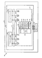
本発明の実施形態は、モデムサブシステムを有するプロセッサにおいて適切に採用されてもよい。図1は、モデムサブシステムにおいてリアルタイム制約を満足するマルチプロセッササブシステム100の実施形態を示す。マルチプロセッササブシステム100は、サブシステムコントローラ104と、フラッシュメモリ、ディスクドライブ、または2つ以上のプロセッサ間で共有される他のデバイスのような、共有デバイス106とを含むデバイスシステムコア102を含む。サブシステムコントローラ104は、アプリケーションプロセッササブシステム(APPS)108と、MSSプロセッサで構成されたモデムサブシステム(MSS)110と、システムバス112と、フラッシュコントローラのような共有デバイスコントローラ114とを含む。APPS108は、製品の要件に従って、1つ、2つ、またはそれ以上のプロセッサで構成されてもよい。APPS108およびMSS110は、システムバス112を介して共有デバイス106にアクセスし、共有デバイスコントローラ114によって制御される。共有デバイス106はまた、取外し可能フラッシュメモリを含むことができるか、または組込み型メモリであってもよい。共有デバイス106が、デバイスシステムコア102においてサブシステムコントローラ104と統合されてもよいことに留意されたい。
Embodiments of the present invention may be suitably employed in a processor having a modem subsystem. FIG. 1 illustrates an embodiment of a
共有デバイスコントローラ114は、共有ホストコントローラインターフェース(HCI)120と、デュアルホスト共有バッファ122と、複数のアトミックアクセスセマフォー124と、APPSシャドーレジスタ126と、MSSシャドーレジスタ128と、共有デバイス106へのアクセスパス129と、ショートタイマー130と、ロングタイマー132とを含み、これらについては後段においてさらに詳細に説明される。APPSの割込み(INT)信号は、ドアベル割込み(DB INT)140と、セマフォー割込み(SEM INT)141と、タイマー割込み(TIM INT)142とを含む。MSSの割込み(INT)信号は、ドアベル割込み(DB INT)144と、セマフォー割込み(SEM INT)145と、タイマー割込み(TIM INT)146とを含む。共有HCI120は、単一のアドレス領域を使用して、共有レジスタのセット、および2つのシャドーレジスタセット(126および128)へのアクセスを提供する。セマフォーは、どちらのシャドーレジスタセットが任意の所与の時点においてHCIアドレス領域にマップされるかを管理する。各プロセッサは、同じアドレススペースを使用してトランザクションを発行する。
The shared
アプリケーションプロセッササブシステム(APPS)108は、APPSシャドーレジスタ126に排他的アクセス権を有し、モデムサブシステム(MSS)110は、MSSシャドーレジスタ128に排他的アクセス権を有する。たとえば、APPS108およびMSS110におけるアクセス制御は、排他的アクセス権を強制するための手段を提供するようにセットアップされてもよい。代替の実施形態において、APPSシャドーレジスタ126は、APPS108のみへのアクセスパスで構成されてもよく、MSSシャドーレジスタ128は、MSS110のみへのアクセスパスで構成されてもよいので、排他的アクセス権を強制するための手段を提供することができる。いずれの場合においても、手段は、APPS108がMSSシャドーレジスタ128にアクセスすることがないように、およびMSS110がAPPSシャドーレジスタ126にアクセスすることがないように提供される。セマフォーは、シャドーレジスタへのアクセスを管理するこのルールをさらに強制する。有利なことに、不揮発性メモリのような共有デバイス106への直接アクセスを有する各プロセッサは、排他的アクセス権を保証するために対応するアクセス制御メカニズムで構成される。
The application processor subsystem (APPS) 108 has exclusive access to the
ショート非アクティブタイマー130は、APPS108またはMSS110からの予想される応答が過剰に遅延する場合に、エラー回復のための割込みを生成するために使用される。たとえば、APPS108がセマフォーを取得しようと試みるが、MSS110が、100msのようなある時間後にセマフォーを解放できない場合、予想される応答の受信がないということは、MSSソフトウェアが現在のタスクに応答していないことの指示である。その場合、ショート非アクティブタイマー130は満了して、エラー回復手順が必要であることをAPPS108に指示する。ロング非アクティブタイマー132は、共有デバイスコントローラ114が、5秒のような長いカウント期間にわたる非ビジー状態を指示する場合、電力制御の割込みを生成するために使用される。共有デバイスコントローラ114がビジー状態になるときは常に、ロング非アクティブタイマーはリセットされ、カウント期間が再始動される。ロングカウント期間に到達した後、共有デバイスコントローラ114および共有デバイス106は、低電力状態におかれる。APPS108またはMSS110のいずれかによるアクセスは、共有デバイスコントローラ114および共有デバイス106の電力を上げて元の状態に戻す。
The
図2Aは、マルチプロセッサデータトランザクションにおいてデータにアクセスするプロセス200の実施形態を示す。プロセス200は、アプリケーションプロセッササブシステム(APPS)202と不揮発性メモリホストコントローラ(NVMHC)206との間、モデムサブシステム(MSS)204とNVMHC206との間、およびNVMHC206とフラッシュデバイス208との間のトランザクションのシーケンスにおいて示される。APPS202は、共有レジスタおよびAPPSシャドーレジスタ126を通じてNVMHC206にアクセスし、MSS204は、共有レジスタおよびMSSシャドーレジスタ128を通じてNVMHC206にアクセスする。一般に、制御アクセスは、シャドーレジスタを通じて達成されるが、一部のモードにおいては、データがシャドーレジスタを通じて同様に転送されてもよい。図2Aおよび図2Bに示されるトランザクションの場合、デバイスが初期化されており、動作可能であって、低減電力モードにないことが想定される。また、共有バッファ122には、後続のトランザクションに必要とされ得る初期化済みデータが取り込まれる。フラッシュデバイス208は、組込み型フラッシュメモリか、または組込み型フラッシュメモリを備える取外し可能セキュアデータカードのいずれかである。
FIG. 2A shows an embodiment of a
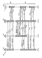
トランザクションの第1のセット201は、APPS202とフラッシュデバイス208との間のデータトランザクションについて示される。トランザクション210において、APPS202は、セマフォーを取得するよう求める要求をNVMHC206に送信する。トランザクション212において、NVMHC206は、セマフォー要求を認可し、セマフォーが取得されたことを指示する応答をAPPS202に送信する。トランザクション214において、APPS202は、フラッシュデバイス208での操作を開始するための第1のコマンド(1st CMD)をNVMHC206に送信する。トランザクション216において、NVMHC206は、データ読取りコマンドのような、第1のコマンドを、フラッシュデバイス208で実行する。トランザクション218において、フラッシュデバイス208は、要求されたデータで、NVMHC206への応答を開始する。トランザクション220において、すべての要求されたデータが読み取られた後、NVMHC206は、フラッシュ操作終了メッセージをAPPS202に送信する。
A first set of
トランザクションの第2のセット221は、MSS204とフラッシュデバイス208との間のデータトランザクションについて示され、APPS202が優先順位の低いコマンドのアクセスセマフォーを取得しようと試みるが、MSS204のトランザクションが発生している。トランザクション222において、MSS204は、セマフォーを取得するよう求める要求をNVMHC206に送信する。トランザクション224において、NVMHC206は、セマフォー要求を認可し、セマフォーが取得されたことを指示する応答をMSS204に送信する。トランザクション226において、MSS204は、フラッシュデバイス208での操作を開始するための第2のコマンド(2nd CMD)をNVMHC206に送信する。トランザクション228において、NVMHC206は、データ読取りコマンドのような、第2のコマンドを、フラッシュデバイス208で実行する。トランザクション230において、フラッシュデバイス208は、要求されたデータで、NVMHC206への応答を開始する。トランザクション232において、APPS202は、セマフォーを取得するよう求める優先順位の低い要求をNVMHC206に送信する。トランザクション234において、MSS204が優先順位の低いAPPS要求よりも高い優先権を有するのでセマフォーに対するAPPS要求が現在認可されず、保留状態にあることを指示するAPPSメッセージがAPPS202に送信され、この場合、MSS204はプリエンプトされ得ない。トランザクション236において、要求されたデータを完了したフラッシュデバイス208は、非ビジー状態メッセージでNVMHC206に応答する。トランザクション238において、すべての要求されたデータが読み取られた後、NVMHC206は、フラッシュデバイス操作終了メッセージをMSS204に送信する。トランザクション240において、NVMHC206は、保留APPSセマフォー要求を認可し、割込みを発行して、保留APPSアクセスセマフォーが取得されたことをAPPS202に通知する。トランザクション242において、APPSは、第3のコマンド(3rd CMD)をNVMHC206に送信する。トランザクション244において、NVMHC206は、データ読取りコマンドのような、第3のコマンドを、フラッシュデバイス208に実行する。トランザクション246において、フラッシュデバイスは、要求されたデータで、NVMHC206への応答を開始する。トランザクション248において、すべての要求されたデータが読み取られた後、NVMHC206は、フラッシュ操作終了メッセージをAPPS202に送信する。
A second set of
図2Bは、リアルタイムタスクにサービスを提供するために、マルチプロセッササブシステムにおいてデータトランザクションをプリエンプトするプロセス250の実施形態を示す。プロセス250は、アプリケーションプロセッササブシステム(APPS)202とセキュアデジタルカードまたは不揮発性メモリホストコントローラ(NVMHC)206と、モデムサブシステム(MSS)204によって優先順位の高い要求により割込みされるフラッシュデバイス208との間のトランザクションのシーケンスにおいて示される。これらのトランザクションの場合、デバイスが初期化されており、動作可能であって、低減電力モードにないことが想定される。フラッシュデバイス208は、組込み型フラッシュメモリか、または組込み型フラッシュメモリを備える取外し可能セキュアデータカードのいずれかである。トランザクション252において、APPS202は、セマフォーを取得するよう求める要求をNVMHC206に送信する。トランザクション254において、NVMHC206は、セマフォー要求を認可し、セマフォーが取得されたことを指示する応答をAPPS202に送信する。トランザクション256において、APPS202は、フラッシュデバイス208での操作を開始するための第1のコマンド(1st CMD)をNVMHC206に送信する。トランザクション258において、NVMHC206は、データ読取りコマンドのような、第1のコマンドを、フラッシュデバイス208で実行する。トランザクション260において、フラッシュデバイス208は、要求されたデータで、NVMHC206への応答を開始する。
FIG. 2B shows an embodiment of a
トランザクション262において、およびAPPSデータトランザクションを完了する前に、MSS204は、セマフォーを取得するよう求める要求をNVMHC206に送信する。トランザクション264において、セマフォーに対するMSS要求が現在認可されず、保留状態にあることを指示するメッセージがMSS204に送信される。トランザクション266において、MSS204がフラッシュデバイス208の優先順位の高いアクセスを試みているので、MSS204は停止要求をNVMHC206に送信する。トランザクション268において、NVMHC206は、ドアベル割込みと称される優先順位の高い割込みをAPPS202に送信して、優先順位の高いMSS要求について通知する。トランザクション270において、APPS202は、ドアベル割込みに応答し、第1のコマンドの実行を停止するためのメッセージをNVMHC206に送信する。トランザクション272において、NVMHC206は、第1のコマンドの実行を停止する。トランザクション274において、フラッシュデバイス208は、ビジー状態ではないことを指示する。トランザクション276において、NVMHC206は、プログラムがプリエンプトされて、第1のコマンドの実行が一時停止されたというメッセージをAPPS202に送信する。トランザクション278において、NVMHC206は、ドアベル割込みをMSS204に発行して、保留中のセマフォーを取得したことをMSS204に通知する。トランザクション280において、MSS204は、第2のコマンド(2nd CMD)をNVMHC206に送信する。トランザクション282において、NVMHC206は、データ読取りコマンドのような、第2のコマンドを、フラッシュデバイス208で実行する。トランザクション284において、フラッシュデバイス208は、要求されたデータで、NVMHC206への応答を開始する。トランザクション286において、要求されたデータトランザクションを完了した後、NVMHC206は、フラッシュ操作終了メッセージをMSS204に送信し、トランザクション287において、MSSはセマフォーを解放する。トランザクション288において、NVMHC206は、第1のコマンドの実行を再始動するかまたは続行すべきであるという割込みをAPPS202に発行する。トランザクション289において、APPS202は、認可されたセマフォーに応答し、1つの実施形態において、APPS202は第1のコマンドを最初から再始動し、別の実施形態においては、APPSは、トランザクション276においてプリエンプトされたポイントから第1のコマンドの実行を続行する。
In
図3は、リアルタイムタスクにサービスを提供するためにデータトランザクションのプリエンプションをサポートするセマフォー状態マシン300の実施形態を示す。セマフォー状態マシン300は、APPS108およびMSS110による共有デバイスコントローラ114へのアクセスを管理する。状態マシン300がIDLE状態304にあるとき、APPS108またはMSS110が、状態マシン300への制御アクセスを取得することができ、それにより共有デバイスコントローラ114へのアクセスを獲得することができる。状態マシン300は、APPS108またはMSS110のいずれかから要求を受信することによって、獲得済みAPPSセマフォー状態306または獲得済みMSSセマフォー状態308のような獲得済み状態に遷移する。たとえば、状態マシン300が、状態306または状態308にあり、他のホストがその他のホストでの既存の操作をプリエンプトするための取得を試みる場合、状態マシン300は、獲得済みAPPSセマフォーと保留MSS要求状態310、または獲得済みMSSセマフォーと保留APPS要求状態312のような獲得済みと保留状態に遷移する。たとえば、状態マシン300が獲得済みAPPSセマフォー状態306にある場合、MSSからの要求を受け入れると、状態マシン300は、対応する獲得済みAPPSセマフォーと保留MSS要求状態310に遷移する。その状態310において、セマフォーを保持しているAPPSがセマフォーを解放すると、状態マシン300は、獲得済みMSSセマフォー状態308に遷移する326。この状態マシン300は、2つのホスト間の制御のハンドオフを加速するために採用される。
FIG. 3 illustrates an embodiment of a
図2Bのトランザクションは、図3の状態マシン300において示される状態遷移と相関関係があってもよい。たとえば、APPS202がセマフォーを要求するトランザクション252は、トランザクション320に対応し、APPS202が認可済みAPPSセマフォーによって指示されるセマフォーを取得するトランザクション254は、状態306に対応する。MSS204は、遷移324に対応する、MSSセマフォーを要求するトランザクション262の取得を試みる。要求は即座には容認されないので、MSS要求保留トランザクション264が発生し、これは状態310に対応する。セマフォーは、トランザクション278においてMSS204に認可され、これは遷移326に対応する。引き続き、トランザクション287においてMSS204がセマフォーを解放することはアイドル状態304に戻る遷移332に対応する。トランザクション289においてAPPS202が認可済みセマフォーに応答することは獲得済みAPPSセマフォー状態306への遷移320に対応する。同様の方法で、MSS204がアイドル状態304にセマフォーを要求することは遷移330に対応し、MSS204がセマフォーを取得することは状態308に対応する。APPS202は、遷移334に対応する取得を試みる。要求が即座には容認されない場合、システムは、状態312においてAPPS要求を保留して獲得済みMSSセマフォーに留まる。APPS要求が認可される場合、MSS204はセマフォーを解放し、アクセスがAPPS202に認可され、これはAPPS202がセマフォーを獲得したことを指示する状態306への遷移336に対応する。
The transaction of FIG. 2B may be correlated with the state transitions shown in the
シャドーレジスタに関して、NVMHC206は、ソフトウェアが、たとえばアプリケーションの初期化時点で、1回構成することを予想する多数のレジスタを含み、それらの値がアプリケーションの動作中に不変のままであることに依存する。複数ホストプロセッサのシナリオにおいて、各ホストプロセッサは、同一のレジスタに異なる値を割り当てようとする場合もあるが、レジスタがそれらの値を保持することを期待している。そのようなストレージ容量の提供に対処するため、シャドーレジスタのセットが各ホストに割り当てられる。シャドーレジスタの各ホストのセットは、セマフォーによって制御されるように単一のアドレススペースにマップされる。セマフォーがホストAに認可される場合、レジスタAのシャドーセットは、ホストAソフトウェアでアクセス可能にされ、値はホストAによってあらかじめ構成されている。その後になって、セマフォーがホストBに認可される場合、レジスタBのシャドーセットは、ホストBソフトウェアでアクセス可能にされるが、レジスタAのシャドーセットは将来の使用のために記憶される。たとえば、シャドーレジスタのAPPSセットおよびシャドーレジスタのMSSセットは、同じ初期状態にリセットされる。読取りアクセスと書込みアクセスの両方についてソフトウェアでアクセス可能にされるシャドーレジスタのセットは、セマフォーの状態によって決定される。APPSがセマフォーを取得すると、APPSシャドーレジスタの値は、共有デバイスコントローラ114内のハードウェアマルチプレクサのような多重化の手段によってAPPSソフトウェアで可視のアドレススペースにマップされる。APPSがセマフォーを取得すると、マルチプレクサがAPPSシャドーレジスタをAPPSソフトウェアで可視にし、MSSがセマフォーを取得すると、MSSシャドーレジスタをMSSソフトウェアで可視にするための手段がハードウェアマルチプレクサによって提供されるというように、セマフォーはハードウェアマルチプレクサを制御する。したがって、共有デバイスにアクセスし、シャドーレジスタの第1のセットへの排他的アクセス権を有するようにするための手段が、第1のプロセッサ、APPSに提供され、共有デバイスにアクセスし、シャドーレジスタの第2のセットへの排他的アクセス権を有するようにするための手段が、第2のプ
ロセッサ、MSSに提供される。APPSソフトウェアは、値を読み取り、任意の値を再構成することができるか、または値をそのAPPSシャドーレジスタ内で不変のままにしておくことができる。MSSソフトウェアが後にセマフォーを取得すると、MSSシャドーレジスタの記憶されている値は、MSSソフトウェアで可視のアドレススペースにマップされ、APPSシャドーレジスタはアクセス不能になる。したがって、共有デバイスコントローラが、セマフォーを第1のプロセッサ、APPS、に認可すると、シャドーレジスタの第1のセットを、共有アドレススペースにマップし、セマフォーを第2のプロセッサ、MSS、に認可すると、シャドーレジスタの第2のセットを、共有アドレススペースにマップするようにするための手段が提供される。セマフォーがアイドル状態にある場合、APPSシャドーレジスタはアドレススペースにマップされてもよく、デフォルト設定としてAPPSソフトウェアでアクセス可能にされてもよい。
With respect to shadow registers,
次の表は、最初にAPPSがデータを転送することで始まり、第2にMSSがデータを転送することが続き、次いで第3にAPPSがデータを転送する、という3つのデータ転送のシナリオにおいてシャドーレジスタの使用を示す。 The following table shows shadows in three data transfer scenarios, starting with APPS transferring data first, followed by MSS transferring data, and thirdly APPS transferring data. Indicates register usage.

上記のシナリオにおいて、MSSがステップ11の後にセマフォーを再取得する場合、DMAチャネル#7を記憶しているMSSシャドーレジスタは、共有アドレススペースにマップされ、MSSソフトウェアがDMAチャネルを変更するようにプログラムされていない限り、MSSソフトウェアはDMAチャネルを再書込みする必要はなくなる。ホスト固有の設定のこの保存は、同じアドレススペースにマップされた他のシャドーレジスタと共に保持される。そのような制御レジスタは、不揮発性メモリまたは2つのホストプロセッサ間で共有される任意の他のデバイスとのすべてのトランザクションについて再構成される必要はない。 In the above scenario, if the MSS reacquires the semaphore after step 11, the MSS shadow register that stores DMA channel # 7 is mapped to the shared address space and the MSS software is programmed to change the DMA channel. Unless it is done, the MSS software does not need to rewrite the DMA channel. This storage of host specific settings is maintained along with other shadow registers mapped to the same address space. Such control registers need not be reconfigured for all transactions with non-volatile memory or any other device shared between the two host processors.
図4は、モデムサブシステムのリアルタイム要求を満足するように構成されるプロセッサ複合体を有するポータブルデバイス400を示す。ポータブルデバイス400は、ワイヤレス電子デバイスであってもよく、ソフトウェア命令410を有するシステムメモリ408に結合されたプロセッサ複合体406を含むシステムコア404を含むことができる。ポータブルデバイス400は、電源414と、アンテナ416と、キーボードのような入力デバイス418と、液晶ディスプレイLCDのようなディスプレイ420と、ビデオ機能を備える1つまたは2つのカメラ422と、スピーカ424と、マイクロフォン426とを備える。システムコア404はまた、ワイヤレスインターフェース428と、ディスプレイコントローラ430と、カメラインターフェース432と、コーデック434とを含む。プロセッサ複合体406は、ローカルレベル1命令およびデータ(L1 I&D)キャッシュ449を有するAPPS CPU1 436と、ローカルレベル1命令およびデータ(L1 I&D)キャッシュ450を有するAPPS CPU2 438という2つの中央演算処理装置を含むプリケーションプロセッササブシステム(APPS)454のデュアルコア配列を含むことができる。APPS454は、図1のAPPS108に対応することができる。プロセッサ複合体406はまた、モデムサブシステム440と、フラッシュコントローラ444と、フラッシュデバイス446と、マルチメディアサブシステム448と、レベル2キャッシュ451と、メモリコントローラ452とを含むことができる。フラッシュデバイス446は、取外し可能フラッシュメモリを含むことができるか、または組込み型メモリであってもよい。モデムサブシステム440は図1のMSS110に対応することができ、フラッシュコントローラ444は図1の共有デバイスコントローラ114に対応することができ、フラッシュデバイス446は図1の共有デバイス106に対応することができる。
FIG. 4 shows a
説明に役立つ例において、システムコア404は、図1、図2A、図2B、および図3において、またはこれらに関連して説明される実施形態のいずれかに従って動作する。たとえば、図4に示されるように、APPS454デュアルコアプロセッサは、図2Aおよび図2Bに示されるデータトランザクションを提供するために、関連するデュアルコアプロセッサのL1 I&Dキャッシュのメモリ、L2キャッシュ451、およびシステムメモリ408に記憶されているデータまたはプログラム命令にアクセスするように構成される。
In an illustrative example, the
ワイヤレスインターフェース428は、アンテナ416およびワイヤレスインターフェース428を介して受信されたワイヤレスデータがMSS440に提供されてAPPS454と共有され得るように、プロセッサ複合体406およびワイヤレスアンテナ416に結合されてもよい。カメラインターフェース432は、プロセッサ複合体406に結合され、さらにビデオ機能を備えるカメラ422のような1つまたは複数のカメラに結合される。ディスプレイコントローラ430は、プロセッサ複合体406、およびディスプレイデバイス420に結合される。コーダ/デコーダ(CODEC)434もまた、プロセッサ複合体406に結合される。ステレオスピーカのペアを備えることができるスピーカ424、およびマイクロフォン426は、CODEC434に結合される。周辺デバイスおよびそれらの関連するインターフェースは、例示的なものであり、数量または容量において限定されることはない。たとえば、入力デバイス418は、ユニバーサルシリアルバス(USB)インターフェースなど、QWERTYスタイルキーボード、英数字キーボード、および特定のデバイスまたは異なるデバイスでの組合せで個別に実装され得る数値パッドを含むことができる。
APPS454は、システムメモリ408のような非一時的コンピュータ可読媒体に記憶され、デュアルコアプロセッサ436および438のようなコンピュータに、プログラムを実行させて図2Aおよび図2Bに示されるデータトランザクションを提供させるために実行可能である、ソフトウェア命令410を実行するように構成される。APPS CPU1 436およびAPPS CPU2 438は、異なるレベルのキャッシュメモリおよびシステムメモリ408からアクセスされるソフトウェア命令410を実行するように構成される。
特定の実施形態において、システムコア404は、システムインパッケージ内、またはシステムオンチップデバイス上に物理的に編成されてもよい。特定の実施形態において、システムオンチップデバイスとして編成されたシステムコア404は、図4に示されるように、電源414と、ワイヤレスアンテナ416と、入力デバイス418と、ディスプレイデバイス420と、カメラまたは複数のカメラ422と、スピーカ424と、マイクロフォン426とに物理的に結合され、取外し可能フラッシュデバイス446に結合されてもよい。
In certain embodiments, the
本明細書において説明される実施形態によるポータブルデバイス400は、セットトップボックス、エンターテイメントユニット、ナビゲーションデバイス、通信デバイス、携帯情報端末(PDA)、固定ロケーションデータユニット、モバイルロケーションデータユニット、携帯電話、セルラー電話、コンピュータ、ポータブルコンピュータ、タブレット、モニタ、コンピュータモニタ、テレビジョン、チューナ、ラジオ、衛星ラジオ、音楽プレイヤー、デジタル音楽プレイヤー、ポータブル音楽プレイヤー、ビデオプレイヤー、デジタルビデオプレイヤー、デジタルビデオディスク(DVD)プレイヤー、ポータブルデジタルビデオプレイヤー、データまたはコンピュータ命令を記憶または取り出す任意の他のデバイスのような、多種多様な電子デバイス、もしくはその任意の組合せに組み込まれてもよい。
The
本明細書において開示される実施形態に関連して説明される様々な例示的な論理ブロック、モジュール、回路、要素、またはコンポーネントは、汎用プロセッサ、デジタル信号プロセッサ(DSP)、特定用途向け集積回路(ASIC)、フィールドプログラマブルゲートアレイ(FPGA)または他のプログラマブル論理コンポーネント、ディスクリートゲートまたはトランジスタ論理、ディスクリートハードウェアコンポーネント、または本明細書において説明される機能を実行するように設計されたこれらの任意の組合せにより実装または実行されてもよい。汎用プロセッサは、マイクロプロセッサであってもよいが、代替策において、プロセッサは、任意の従来のプロセッサ、コントローラ、マイクロコントローラ、または状態マシンであってもよい。プロセッサはまた、たとえばDSPとマイクロプロセッサの組合せのようなコンピューティングコンポーネントの組合せ、複数のマイクロプロセッサ、DSPコアと併せた1つまたは複数のマイクロプロセッサ、または望ましいアプリケーションに適した任意の他のそのような構成として実装されてもよい。 Various exemplary logic blocks, modules, circuits, elements, or components described in connection with the embodiments disclosed herein are general purpose processors, digital signal processors (DSPs), application specific integrated circuits ( ASIC), Field Programmable Gate Array (FPGA) or other programmable logic components, discrete gate or transistor logic, discrete hardware components, or any combination thereof designed to perform the functions described herein May be implemented or implemented. A general purpose processor may be a microprocessor, but in the alternative, the processor may be any conventional processor, controller, microcontroller, or state machine. The processor can also be a combination of computing components, such as a combination of DSP and microprocessor, multiple microprocessors, one or more microprocessors in conjunction with a DSP core, or any other such suitable for the desired application. It may be implemented as a simple configuration.
たとえば、図1のAPPS108または図4のデュアルコアプロセッサ436および438は、たとえば、プログラムの制御下でリアルタイムタスクにサービスを提供するために、マルチプロセッサシステムにおいてデータトランザクションをプリエンプトできるようにする命令を実行するように構成されてもよい。プロセッサ複合体406にローカルに直接関連付けられているコンピュータ可読非一時的ストレージ媒体上に記憶されているプログラムは、たとえば命令キャッシュを通じて使用可能であっても、または特定の入力デバイス418またはワイヤレスインターフェース428を通じてアクセス可能であってもよい。たとえば、入力デバイス418またはワイヤレスインターフェース428はまた、プロセッサローカルデータキャッシュのようなプロセッサにローカルに直接関連付けられているか、またはシステムメモリ408からアクセス可能なメモリデバイスに存在するデータにアクセスすることもできる。本明細書において開示される様々な実施形態に関連して説明される方法は、ハードウェアにおいて、プロセッサによって実行される1つまたは複数のプログラムを有するソフトウェアモジュールにおいて、またはこの2つの組合せにおいて直接具現されてもよい。ソフトウェアモジュールは、ランダムアクセスメモリ(RAM)、ダイナミックランダムアクセスメモリ(DRAM)、同期ダイナミックランダムアクセスメモリ(SDRAM)、フラッシュメモリ、読取り専用メモリ(ROM)、消去可能プログラマブル読取り専用メモリ(EPROM)、電気的消去可能プログラマブル読取り専用メモリ(EEPROM)、ハードディスク、取外し可能ディスク、コンパクトディスク(CD)-ROM、デジタルビデオディスク(DVD)、または当技術分野において知られている任意の他の形態の非一時的ストレージ媒体に存在することができる。非一時的ストレージ媒体は、プロセッサがストレージ媒体から情報を読み取り、ストレージ媒体に情報を書き込むことができるように、プロセッサに結合されてもよい。代替策において、ストレージ媒体は、プロセッサに組込み型であってもよい。
For example,
本発明は、プロセッサシステムにおいて使用される例示的な実施形態のコンテキストにおいて開示されるが、上記の説明および以下に続く特許請求の範囲と一致する、多岐にわたる実施態様が、当業者によって採用され得ることが理解されるであろう。たとえば、固定機能の実装態様はまた、本発明の様々な実施形態を使用することもできる。 Although the invention is disclosed in the context of exemplary embodiments used in a processor system, a wide variety of embodiments consistent with the above description and the claims that follow can be employed by those skilled in the art. It will be understood. For example, fixed function implementations may also use various embodiments of the present invention.
100 マイクロプロセッササブシステム
102 デバイスシステムコア
104 サブシステムコントローラ
106 共有デバイス
108 アプリケーションプロセッササブシステム(APPS)
110 モデムサブシステム(MSS)
112 システムバス
114 共有デバイスコントローラ
120 共有HCI
122 デュアルホスト共有バッファ
124 セマフォー
126 シャドーレジスタAPPS
128 シャドーレジスタMSM
130 ショートタイマー
132 ロングタイマー
208 フラッシュデバイス
406 プロセッサ複合体
408 システムメモリ
410 ソフトウェア(たとえば、命令)
414 電源
418 入力デバイス
420 ディスプレイ
422 カメラ(ビデオ)
424 スピーカ
426 マイクロフォン
428 ワイヤレスインターフェース
430 ディスプレイコントローラ
432 カメラインターフェース
434 コーデック
436 アプリケーションサブシステムコアプロセッサ1
438 アプリケーションサブシステムコアプロセッサ2
440 モデムサブシステム(MSS)
444 フラッシュコントローラ
446 フラッシュデバイス
448 マルチメディアサブシステム
449 L1 I&Dキャッシュ
450 L1 I&Dキャッシュ
451 メモリコントローラ
100 microprocessor subsystem
102 Device system core
104 Subsystem controller
106 Shared devices
108 Application Processor Subsystem (APPS)
110 Modem subsystem (MSS)
112 System bus
114 Shared device controller
120 shared HCI
122 Dual host shared buffer
124 Semaphore
126 Shadow Register APPS
128 Shadow register MSM
130 short timer
132 Long timer
208 flash devices
406 processor complex
408 system memory
410 software (for example, instructions)
414 power supply
418 input devices
420 display
422 Camera (video)
424 speaker
426 microphone
428 wireless interface
430 display controller
432 Camera interface
434 codec
436 Application Subsystem Core Processor 1
438 Application Subsystem Core Processor 2
440 modem subsystem (MSS)
444 flash controller
446 flash device
448 Multimedia Subsystem
449 L1 I & D Cash
450 L1 I & D cash
451 Memory controller
Claims (17)
直接アクセスによって前記第1のプロセッサおよび第2のプロセッサと共有される共有不揮発性メモリデバイスから前記第1のプロセッサによりデータアクセスを実施するステップと、
前記第1のプロセッサによる前記共有不揮発性メモリデバイスへの前記第1のプロセッサによる操作のプリエンプションを要求するために、前記第1のプロセッサにドアベル割込みを発行するステップと、
前記第1のプロセッサによる前記データアクセスをプリエンプトし、前記第2のプロセッサによるメモリアクセスを開始するステップと、
を含み、
前記第1のプロセッサは、シャドーレジスタの第1のセットに対する排他的アクセス権を有し、シャドーレジスタの前記第1のセットにアクセスするように構成され、シャドーレジスタの前記第1のセットの各シャドーレジスタは、アドレスマップされたレジスタが共有アドレススペースにマップされるように前記共有アドレススペースにリンクされるように構成された前記アドレスマップされたレジスタを含み、
前記第2のプロセッサは、シャドーレジスタの第2のセットに対する排他的アクセス権を有し、シャドーレジスタの前記第2のセットにアクセスするように構成され、シャドーレジスタの前記第2のセットの各シャドーレジスタは、アドレスマップされたレジスタが共有アドレススペースにマップされるように前記共有アドレススペースにリンクされるように構成された前記アドレスマップされたレジスタを含み、
前記第1のプロセッサにより前記データアクセスを実施するステップは、シャドーレジスタの前記第1のセットにアクセスするステップを含み、
前記第2のプロセッサにより前記メモリアクセスを開始するステップは、シャドーレジスタの前記第2のセットにアクセスするステップを含む、
方法。 A method for preempting a first processor by a second processor, comprising:
Performing data access by the first processor from a shared non-volatile memory device shared with the first processor and the second processor by direct access;
Issuing a doorbell interrupt to the first processor to request preemption of the operation by the first processor to the shared non-volatile memory device by the first processor;
Preempting the data access by the first processor and initiating memory access by the second processor;
Including
Wherein the first processor is configured to have a exclusive access to the first set of shadow registers, adapted to access said first set of shadow registers, each shadow of the first set of shadow registers A register comprising the address mapped register configured to be linked to the shared address space such that the address mapped register is mapped to the shared address space;
The second processor is configured to have a exclusive access to the second set of shadow registers, configured to access said second set of shadow registers, each shadow of the second set of shadow registers A register comprising the address mapped register configured to be linked to the shared address space such that the address mapped register is mapped to the shared address space;
Performing the data access by the first processor comprises accessing the first set of shadow registers;
Initiating the memory access by the second processor comprises accessing the second set of shadow registers;
Method.
前記第1のプロセッサにより前記データアクセスを再開するステップと、
をさらに備える請求項1に記載の方法。 Completing the access by the second processor;
Resuming the data access by the first processor;
The method of claim 1, further comprising:
前記第2のプロセッサが前記メモリアクセスを完了した後に、前記データアクセスを再開するために、前記第1のプロセッサにセマフォロックを認可するステップと
をさらに備える請求項1に記載の方法。 Granting a semaphore lock to the second processor to initiate the memory access to the shared non-volatile memory device;
The method of claim 1, further comprising granting a semaphore lock to the first processor to resume the data access after the second processor completes the memory access.
共有アドレススペースと、
シャドーレジスタの第1のセットであって、シャドーレジスタの前記第1のセットの各シャドーレジスタは、アドレスマップされたレジスタが共有アドレススペースにマップされるように前記共有アドレススペースにリンクされるように構成された前記アドレスマップされたレジスタを含む、シャドーレジスタの第1のセットと、
シャドーレジスタの第2のセットであって、シャドーレジスタの前記第2のセットの各シャドーレジスタは、アドレスマップされたレジスタが共有アドレススペースにマップされるように前記共有アドレススペースにリンクされるように構成された前記アドレスマップされたレジスタを含む、シャドーレジスタの第2のセットと、
を備える、共有デバイスコントローラと、
前記共有デバイスコントローラを介して共有デバイスに接続され、シャドーレジスタの第1のセットに対して排他的アクセス権を有するように構成された、第1のプロセッサと、
前記共有デバイスコントローラを介して前記共有デバイスに接続され、シャドーレジスタの第2のセットに対して排他的アクセス権を有するように構成された、第2のプロセッサと、
を備え、
前記共有デバイスコントローラは、セマフォを前記第1のプロセッサに認可すると、シャドーレジスタの前記第1のセットを前記共有アドレススペースにマップし、前記セマフォを前記第2のプロセッサに認可すると、シャドーレジスタの前記第2のセットを前記共有アドレススペースにマップするように構成されたセマフォ状態マシンを有する、
を備える装置。 A device that allows two processors to independently access a shared device,
A shared address space;
A first set of shadow registers, such that each shadow register of the first set of shadow registers is linked to the shared address space such that an address-mapped register is mapped to the shared address space A first set of shadow registers, including the configured address-mapped registers;
A second set of shadow registers, wherein each shadow register of the second set of shadow registers is linked to the shared address space such that an address-mapped register is mapped to the shared address space A second set of shadow registers, including the configured address-mapped registers;
A shared device controller comprising:
A first processor connected to the shared device via the shared device controller and configured to have exclusive access to the first set of shadow registers;
A second processor connected to the shared device via the shared device controller and configured to have exclusive access to a second set of shadow registers;
With
When the shared device controller authorizes a semaphore to the first processor, the shared device controller maps the first set of shadow registers to the shared address space, and grants the semaphore to the second processor, the shadow register Having a semaphore state machine configured to map a second set to the shared address space;
A device comprising:
第1のアドレスマップされたレジスタへのアクセスが共有アドレスにマップされるように前記共有アドレスにリンクされるように構成された前記第1のアドレスマップされたレジスタを含む、第1のシャドーレジスタを、第1のプロセッサによるセマフォの取得に応答して、前記共有アドレスにマップするステップであって、前記第1のプロセッサが、第1の値を前記共有アドレスにおいて前記第1のシャドーレジスタに書き込む、ステップと、
前記第1のプロセッサによる共有デバイスへの第1の操作の完了時の前記セマフォの解放に応答して、前記第1のシャドーレジスタを前記共有アドレスからリンク除去するステップと、
第2のアドレスマップされたレジスタへのアクセスが共有アドレスにマップされるように前記共有アドレスにリンクされるように構成された前記第2のアドレスマップされたレジスタを含む、第2のシャドーレジスタを、第2のプロセッサによるセマフォの取得に応答して、前記共有アドレスにマップするステップであって、前記第2のプロセッサが、第2の値を前記共有アドレスにおいて前記第2のシャドーレジスタに書き込む、ステップと、
前記第2のプロセッサによる前記共有デバイスへの第2の操作の完了時の前記セマフォの解放に応答して、前記第2のシャドーレジスタを前記共有アドレスからリンク除去するステップであって、前記第2の操作の完了時に、前記第1の値は前記第1のシャドーレジスタ内で不変であり、前記第2の値は前記第2のシャドーレジスタ内で不変である、ステップと を備える方法。 A method for allowing two processors to independently access a shared device,
A first shadow register comprising the first address mapped register configured to be linked to the shared address such that access to the first address mapped register is mapped to the shared address; Mapping to the shared address in response to obtaining a semaphore by a first processor, wherein the first processor writes a first value to the first shadow register at the shared address; Steps,
Linking the first shadow register from the shared address in response to releasing the semaphore upon completion of a first operation to the shared device by the first processor;
A second shadow register comprising the second address mapped register configured to be linked to the shared address such that access to the second address mapped register is mapped to the shared address; Mapping to the shared address in response to obtaining a semaphore by a second processor, wherein the second processor writes a second value to the second shadow register at the shared address; Steps,
Linking the second shadow register from the shared address in response to releasing the semaphore upon completion of a second operation on the shared device by the second processor, the second processor comprising: The first value is unchanged in the first shadow register and the second value is unchanged in the second shadow register upon completion of the operation.
第1のアドレスマップされたレジスタへのアクセスが共有アドレスにマップされるように前記共有アドレスにリンクされるように構成された前記第1のアドレスマップされたレジスタを含む、第1のシャドーレジスタを、第1のプロセッサによるセマフォの取得に応答して、前記共有アドレスにマップするステップであって、前記第1のプロセッサが、第1の値を前記共有アドレスにおいて前記第1のシャドーレジスタに書き込む、ステップと、
前記第1のプロセッサによる共有デバイスへの第1の操作の完了時の前記セマフォの解放に応答して、前記第1のシャドーレジスタを前記共有アドレスからリンク除去するステップと、
第2のアドレスマップされたレジスタへのアクセスが共有アドレスにマップされるように前記共有アドレスにリンクされるように構成された前記第2のアドレスマップされたレジスタを含む、第2のシャドーレジスタを、第2のプロセッサによるセマフォの取得に応答して、前記共有アドレスにマップするステップであって、前記第2のプロセッサが、第2の値を前記共有アドレスにおいて前記第2のシャドーレジスタに書き込む、ステップと、
前記第2のプロセッサによる前記共有デバイスへの第2の操作の完了時の前記セマフォの解放に応答して、前記第2のシャドーレジスタを前記共有アドレスからリンク除去するステップであって、前記第2の操作の完了時に、前記第1の値は前記第1のシャドーレジスタ内で不変であり、前記第2の値は前記第2のシャドーレジスタ内で不変である、ステップとを実施するように動作可能である、コンピュータ可読非一時的記憶媒体。 A computer readable non-transitory storage medium encoded with computer readable program data and code when the program data and code are executed by a processor,
A first shadow register comprising the first address mapped register configured to be linked to the shared address such that access to the first address mapped register is mapped to the shared address; Mapping to the shared address in response to obtaining a semaphore by a first processor, wherein the first processor writes a first value to the first shadow register at the shared address; Steps,
Linking the first shadow register from the shared address in response to releasing the semaphore upon completion of a first operation to the shared device by the first processor;
A second shadow register comprising the second address mapped register configured to be linked to the shared address such that access to the second address mapped register is mapped to the shared address; Mapping to the shared address in response to obtaining a semaphore by a second processor, wherein the second processor writes a second value to the second shadow register at the shared address; Steps,
Linking the second shadow register from the shared address in response to releasing the semaphore upon completion of a second operation on the shared device by the second processor, the second processor comprising: The first value is invariant in the first shadow register and the second value is invariant in the second shadow register upon completion of the operation A possible computer-readable non-transitory storage medium.
直接アクセスによって第1のプロセッサおよび第2のプロセッサと共有される共有不揮発性メモリデバイスから前記第1のプロセッサによりデータアクセスを実施するステップと、
前記第1のプロセッサによる前記共有不揮発性メモリデバイスへの前記第1のプロセッサによる操作のプリエンプションを要求するために、前記第1のプロセッサにドアベル割込みを発行するステップと、
前記第1のプロセッサによる前記データアクセスをプリエンプトし、前記第2のプロセッサによるメモリアクセスを開始するステップと、
を実施するように動作可能であり、
前記第1のプロセッサは、シャドーレジスタの第1のセットに対する排他的アクセス権を有し、シャドーレジスタの前記第1のセットにアクセスするように構成され、シャドーレジスタの前記第1のセットの各シャドーレジスタは、アドレスマップされたレジスタが共有アドレススペースにマップされるように前記共有アドレススペースにリンクされるように構成された前記アドレスマップされたレジスタを含み、
前記第2のプロセッサは、シャドーレジスタの第2のセットに対する排他的アクセス権を有し、シャドーレジスタの前記第2のセットにアクセスするように構成され、シャドーレジスタの前記第2のセットの各シャドーレジスタは、アドレスマップされたレジスタが共有アドレススペースにマップされるように前記共有アドレススペースにリンクされるように構成された前記アドレスマップされたレジスタを含み、
前記第1のプロセッサにより前記データアクセスを実施するステップは、シャドーレジスタの前記第1のセットにアクセスするステップを含み、
前記第2のプロセッサにより前記メモリアクセスを開始するステップは、シャドーレジスタの前記第2のセットにアクセスするステップを含む、
コンピュータ可読非一時的記憶媒体。 A computer readable non-transitory storage medium encoded with computer readable program data and code when the program data and code are executed by a processor,
Performing data access by the first processor from a shared non-volatile memory device shared with the first processor and the second processor by direct access;
Issuing a doorbell interrupt to the first processor to request preemption of the operation by the first processor to the shared non-volatile memory device by the first processor;
Preempting the data access by the first processor and initiating memory access by the second processor;
Is operable to carry out
Wherein the first processor is configured to have a exclusive access to the first set of shadow registers, adapted to access said first set of shadow registers, each shadow of the first set of shadow registers A register comprising the address mapped register configured to be linked to the shared address space such that the address mapped register is mapped to the shared address space;
The second processor is configured to have a exclusive access to the second set of shadow registers, configured to access said second set of shadow registers, each shadow of the second set of shadow registers A register comprising the address mapped register configured to be linked to the shared address space such that the address mapped register is mapped to the shared address space;
Performing the data access by the first processor comprises accessing the first set of shadow registers;
Initiating the memory access by the second processor comprises accessing the second set of shadow registers;
A computer-readable non-transitory storage medium.
第1のプロセッサが共有デバイスにアクセスし、シャドーレジスタの第1のセットへの排他的アクセス権を有するための手段であって、シャドーレジスタの前記第1のセットの各シャドーレジスタは、アドレスマップされたレジスタが共有アドレススペースにマップされるように前記共有アドレススペースにリンクされるように構成された前記アドレスマップされたレジスタを含む、手段と、
第2のプロセッサが共有デバイスにアクセスし、シャドーレジスタの第2のセットへの排他的アクセス権を有するための手段であって、シャドーレジスタの前記第2のセットの各シャドーレジスタは、アドレスマップされたレジスタが共有アドレススペースにマップされるように前記共有アドレススペースにリンクされるように構成された前記アドレスマップされたレジスタを含む、手段と、
共有デバイスコントローラが、セマフォを前記第1のプロセッサに認可すると、シャドーレジスタの前記第1のセットを前記共有アドレススペースにマップし、前記セマフォを前記第2のプロセッサに認可すると、シャドーレジスタの前記第2のセットを前記共有アドレススペースにマップするための手段と、
を備える装置。 A device that allows two processors to independently access a shared device,
Means for a first processor to access a shared device and have exclusive access to a first set of shadow registers, each shadow register of said first set of shadow registers being address mapped Means comprising: said address mapped register configured to be linked to said shared address space such that said registered register is mapped to said shared address space;
Means for a second processor to access a shared device and have exclusive access to a second set of shadow registers, each shadow register of said second set of shadow registers being address mapped Means comprising: said address mapped register configured to be linked to said shared address space such that said registered register is mapped to said shared address space;
When a shared device controller authorizes a semaphore to the first processor, it maps the first set of shadow registers to the shared address space, and authorizes the semaphore to the second processor, the first register of shadow registers. Means for mapping a set of two to the shared address space;
A device comprising:
Applications Claiming Priority (3)
| Application Number | Priority Date | Filing Date | Title |
|---|---|---|---|
| US13/798,803 | 2013-03-13 | ||
| US13/798,803 US9431077B2 (en) | 2013-03-13 | 2013-03-13 | Dual host embedded shared device controller |
| PCT/US2014/021834 WO2014164310A1 (en) | 2013-03-13 | 2014-03-07 | Dual host embedded shared device controller |
Publications (3)
| Publication Number | Publication Date |
|---|---|
| JP2016512361A JP2016512361A (en) | 2016-04-25 |
| JP2016512361A5 JP2016512361A5 (en) | 2017-01-19 |
| JP6181844B2 true JP6181844B2 (en) | 2017-08-16 |
Family
ID=50473781
Family Applications (1)
| Application Number | Title | Priority Date | Filing Date |
|---|---|---|---|
| JP2016500857A Active JP6181844B2 (en) | 2013-03-13 | 2014-03-07 | Dual Host Embedded Shared Device Controller |
Country Status (5)
| Country | Link |
|---|---|
| US (1) | US9431077B2 (en) |
| EP (1) | EP2972860B1 (en) |
| JP (1) | JP6181844B2 (en) |
| CN (1) | CN105190561B (en) |
| WO (1) | WO2014164310A1 (en) |
Families Citing this family (9)
| Publication number | Priority date | Publication date | Assignee | Title |
|---|---|---|---|---|
| USRE49652E1 (en) | 2013-12-16 | 2023-09-12 | Qualcomm Incorporated | Power saving techniques in computing devices |
| WO2018038703A1 (en) * | 2016-08-22 | 2018-03-01 | Hewlett-Packard Development Company, L.P. | Connected devices information |
| IT201700034731A1 (en) | 2017-03-29 | 2018-09-29 | St Microelectronics Srl | MODULE AND METHOD OF MANAGEMENT OF ACCESS TO A MEMORY |
| CN107357666B (en) * | 2017-06-26 | 2020-04-21 | 西安微电子技术研究所 | Multi-core parallel system processing method based on hardware protection |
| US10769092B2 (en) * | 2018-12-20 | 2020-09-08 | Dell Products, L.P. | Apparatus and method for reducing latency of input/output transactions in an information handling system using no-response commands |
| TWI716167B (en) * | 2019-10-29 | 2021-01-11 | 新唐科技股份有限公司 | Storage devices and mapping methods thereof |
| US11561912B2 (en) | 2020-06-01 | 2023-01-24 | Samsung Electronics Co., Ltd. | Host controller interface using multiple circular queue, and operating method thereof |
| US11755518B2 (en) * | 2021-06-28 | 2023-09-12 | Dell Products L.P. | Control of Thunderbolt/DisplayPort multiplexor for discrete USB-C graphics processor |
| CN113835757B (en) * | 2021-09-29 | 2023-08-15 | 深圳大普微电子科技有限公司 | Method and device for sharing register model by multiple hosts and electronic equipment |
Family Cites Families (30)
| Publication number | Priority date | Publication date | Assignee | Title |
|---|---|---|---|---|
| WO1984004190A1 (en) | 1983-04-15 | 1984-10-25 | Convergent Technologies Inc | Multi-computer computer architecture |
| US6018785A (en) | 1993-12-30 | 2000-01-25 | Cypress Semiconductor Corp. | Interrupt-generating hardware semaphore |
| US5854638A (en) * | 1996-02-02 | 1998-12-29 | Opti Inc. | Unified memory architecture with parallel access by host and video controller |
| US6006303A (en) * | 1997-08-28 | 1999-12-21 | Oki Electric Industry Co., Inc. | Priority encoding and decoding for memory architecture |
| US6163831A (en) | 1997-11-14 | 2000-12-19 | Lucent Technologies, Inc. | Minimum refractory period in a multiple agent resource sharing environment |
| US6314501B1 (en) | 1998-07-23 | 2001-11-06 | Unisys Corporation | Computer system and method for operating multiple operating systems in different partitions of the computer system and for allowing the different partitions to communicate with one another through shared memory |
| US6393590B1 (en) | 1998-12-22 | 2002-05-21 | Nortel Networks Limited | Method and apparatus for ensuring proper functionality of a shared memory, multiprocessor system |
| JP2001216284A (en) * | 1999-11-25 | 2001-08-10 | Denso Corp | Electronic control unit |
| DE10048732A1 (en) * | 2000-09-29 | 2002-04-18 | Philips Corp Intellectual Pty | Multiprocessor arrangement |
| US6874049B1 (en) | 2001-02-02 | 2005-03-29 | Cradle Technologies, Inc. | Semaphores with interrupt mechanism |
| JP3704573B2 (en) | 2001-03-14 | 2005-10-12 | 東芝ソリューション株式会社 | Cluster system |
| US7206776B2 (en) | 2002-08-15 | 2007-04-17 | Microsoft Corporation | Priority differentiated subtree locking |
| US7979048B2 (en) | 2005-09-15 | 2011-07-12 | Silicon Laboratories Inc. | Quasi non-volatile memory for use in a receiver |
| US7421529B2 (en) * | 2005-10-20 | 2008-09-02 | Qualcomm Incorporated | Method and apparatus to clear semaphore reservation for exclusive access to shared memory |
| US8209527B2 (en) | 2006-10-26 | 2012-06-26 | Samsung Electronics Co., Ltd. | Memory system and memory management method including the same |
| US7512723B2 (en) * | 2006-12-29 | 2009-03-31 | Freescale Semiconductor, Inc. | Queued interface devices, multi-core peripheral systems, and methods for sharing a peripheral in a multi-core system |
| US8185685B2 (en) * | 2007-12-14 | 2012-05-22 | Hitachi Global Storage Technologies Netherlands B.V. | NAND flash module replacement for DRAM module |
| KR20090095955A (en) | 2008-03-07 | 2009-09-10 | 삼성전자주식회사 | Multi port semiconductor memory device for providing direct access function in shared structure of non-volatile memory and multi processor system having the same |
| JP2009277007A (en) * | 2008-05-14 | 2009-11-26 | Mitsubishi Electric Corp | Computer device and program |
| JP5241384B2 (en) | 2008-08-29 | 2013-07-17 | ルネサスエレクトロニクス株式会社 | Distributed shared memory multiprocessor and data processing method |
| KR20100041309A (en) * | 2008-10-14 | 2010-04-22 | 삼성전자주식회사 | Multi processor system utilizing application functions in each processor |
| US8751843B2 (en) | 2008-12-16 | 2014-06-10 | The Regents Of The University Of Michigan | Computer energy conservation with a scalable PSU configuration |
| KR20110013867A (en) | 2009-08-04 | 2011-02-10 | 삼성전자주식회사 | Multi processor system having flash-less booting function in memory link architecture |
| US8639852B2 (en) * | 2009-11-13 | 2014-01-28 | Qualcomm Incorporated | Burst access protocol |
| JP2011232956A (en) * | 2010-04-27 | 2011-11-17 | Clarion Co Ltd | Computer system and program |
| US8850262B2 (en) | 2010-10-12 | 2014-09-30 | International Business Machines Corporation | Inter-processor failure detection and recovery |
| US8438416B2 (en) | 2010-10-21 | 2013-05-07 | Advanced Micro Devices, Inc. | Function based dynamic power control |
| CA2823732A1 (en) | 2011-03-25 | 2012-10-04 | Research In Motion Limited | Dynamic power management of cache memory in a multi-core processing system |
| US8745427B2 (en) | 2011-08-10 | 2014-06-03 | Intel Corporation | Memory link power management |
| US9400677B2 (en) * | 2013-01-02 | 2016-07-26 | Apple Inc. | Adaptive handling of priority inversions using transactions |
-
2013
- 2013-03-13 US US13/798,803 patent/US9431077B2/en active Active
-
2014
- 2014-03-07 JP JP2016500857A patent/JP6181844B2/en active Active
- 2014-03-07 EP EP14716473.5A patent/EP2972860B1/en active Active
- 2014-03-07 WO PCT/US2014/021834 patent/WO2014164310A1/en active Application Filing
- 2014-03-07 CN CN201480013506.4A patent/CN105190561B/en not_active Expired - Fee Related
Also Published As
| Publication number | Publication date |
|---|---|
| US9431077B2 (en) | 2016-08-30 |
| CN105190561A (en) | 2015-12-23 |
| US20140281283A1 (en) | 2014-09-18 |
| EP2972860A1 (en) | 2016-01-20 |
| JP2016512361A (en) | 2016-04-25 |
| WO2014164310A1 (en) | 2014-10-09 |
| EP2972860B1 (en) | 2021-03-03 |
| CN105190561B (en) | 2018-04-20 |
Similar Documents
| Publication | Publication Date | Title |
|---|---|---|
| JP6181844B2 (en) | Dual Host Embedded Shared Device Controller | |
| JP5963282B2 (en) | Interrupt distribution scheme | |
| US9400677B2 (en) | Adaptive handling of priority inversions using transactions | |
| KR102219545B1 (en) | Mid-thread pre-emption with software assisted context switch | |
| US9405687B2 (en) | Method, apparatus and system for handling cache misses in a processor | |
| US9600618B2 (en) | Implementing system irritator accelerator FPGA unit (AFU) residing behind a coherent attached processors interface (CAPI) unit | |
| JP2012038293A (en) | Multiprocessor system on-chip for machine vision | |
| US9881680B2 (en) | Multi-host power controller (MHPC) of a flash-memory-based storage device | |
| JP5578713B2 (en) | Information processing device | |
| US20150347017A1 (en) | Command trapping in an input/output virtualization (iov) host controller (hc) (iov-hc) of a flash-memory-based storage device | |
| US20140129751A1 (en) | Hybrid interface to improve semiconductor memory based ssd performance | |
| US20160026436A1 (en) | Dynamic Multi-processing In Multi-core Processors | |
| US20160275026A1 (en) | Weakly ordered doorbell | |
| CN109716305B (en) | Method, computing device, and medium for implementing asynchronous cache maintenance operations | |
| US20130055284A1 (en) | Managing shared computer resources | |
| US8972624B2 (en) | USB virtualization | |
| US9047264B2 (en) | Low pin count controller | |
| US9563586B2 (en) | Shims for processor interface | |
| TW201435570A (en) | Periodic activity alignment | |
| JP2016513838A (en) | Security coprocessor boot performance | |
| KR20150090621A (en) | Storage device and method for data processing | |
| JP2014157392A (en) | Semiconductor device and data processing system | |
| WO2018107394A1 (en) | I/o emulation abortion in virtualized environments | |
| US20090077322A1 (en) | System and Method for Getllar Hit Cache Line Data Forward Via Data-Only Transfer Protocol Through BEB Bus |
Legal Events
| Date | Code | Title | Description |
|---|---|---|---|
| A521 | Request for written amendment filed |
Free format text: JAPANESE INTERMEDIATE CODE: A523 Effective date: 20161128 |
|
| A621 | Written request for application examination |
Free format text: JAPANESE INTERMEDIATE CODE: A621 Effective date: 20161128 |
|
| A871 | Explanation of circumstances concerning accelerated examination |
Free format text: JAPANESE INTERMEDIATE CODE: A871 Effective date: 20161128 |
|
| A975 | Report on accelerated examination |
Free format text: JAPANESE INTERMEDIATE CODE: A971005 Effective date: 20170309 |
|
| A131 | Notification of reasons for refusal |
Free format text: JAPANESE INTERMEDIATE CODE: A131 Effective date: 20170313 |
|
| A521 | Request for written amendment filed |
Free format text: JAPANESE INTERMEDIATE CODE: A523 Effective date: 20170612 |
|
| TRDD | Decision of grant or rejection written | ||
| A01 | Written decision to grant a patent or to grant a registration (utility model) |
Free format text: JAPANESE INTERMEDIATE CODE: A01 Effective date: 20170626 |
|
| A61 | First payment of annual fees (during grant procedure) |
Free format text: JAPANESE INTERMEDIATE CODE: A61 Effective date: 20170720 |
|
| R150 | Certificate of patent or registration of utility model |
Ref document number: 6181844 Country of ref document: JP Free format text: JAPANESE INTERMEDIATE CODE: R150 |
|
| R250 | Receipt of annual fees |
Free format text: JAPANESE INTERMEDIATE CODE: R250 |
|
| R250 | Receipt of annual fees |
Free format text: JAPANESE INTERMEDIATE CODE: R250 |
|
| R250 | Receipt of annual fees |
Free format text: JAPANESE INTERMEDIATE CODE: R250 |
|
| R250 | Receipt of annual fees |
Free format text: JAPANESE INTERMEDIATE CODE: R250 |