JP6156886B2 - System and method for reducing transmitter power consumption - Google Patents
System and method for reducing transmitter power consumption Download PDFInfo
- Publication number
- JP6156886B2 JP6156886B2 JP2015503232A JP2015503232A JP6156886B2 JP 6156886 B2 JP6156886 B2 JP 6156886B2 JP 2015503232 A JP2015503232 A JP 2015503232A JP 2015503232 A JP2015503232 A JP 2015503232A JP 6156886 B2 JP6156886 B2 JP 6156886B2
- Authority
- JP
- Japan
- Prior art keywords
- potential
- transmitter
- electrode
- transmitter electrode
- input device
- Prior art date
- Legal status (The legal status is an assumption and is not a legal conclusion. Google has not performed a legal analysis and makes no representation as to the accuracy of the status listed.)
- Active
Links
Images


Classifications
-
- G—PHYSICS
- G06—COMPUTING; CALCULATING OR COUNTING
- G06F—ELECTRIC DIGITAL DATA PROCESSING
- G06F3/00—Input arrangements for transferring data to be processed into a form capable of being handled by the computer; Output arrangements for transferring data from processing unit to output unit, e.g. interface arrangements
- G06F3/01—Input arrangements or combined input and output arrangements for interaction between user and computer
- G06F3/03—Arrangements for converting the position or the displacement of a member into a coded form
- G06F3/041—Digitisers, e.g. for touch screens or touch pads, characterised by the transducing means
- G06F3/044—Digitisers, e.g. for touch screens or touch pads, characterised by the transducing means by capacitive means
-
- G—PHYSICS
- G06—COMPUTING; CALCULATING OR COUNTING
- G06F—ELECTRIC DIGITAL DATA PROCESSING
- G06F1/00—Details not covered by groups G06F3/00 - G06F13/00 and G06F21/00
- G06F1/26—Power supply means, e.g. regulation thereof
- G06F1/32—Means for saving power
- G06F1/3203—Power management, i.e. event-based initiation of a power-saving mode
- G06F1/3234—Power saving characterised by the action undertaken
- G06F1/325—Power saving in peripheral device
- G06F1/3262—Power saving in digitizer or tablet
-
- G—PHYSICS
- G06—COMPUTING; CALCULATING OR COUNTING
- G06F—ELECTRIC DIGITAL DATA PROCESSING
- G06F3/00—Input arrangements for transferring data to be processed into a form capable of being handled by the computer; Output arrangements for transferring data from processing unit to output unit, e.g. interface arrangements
- G06F3/01—Input arrangements or combined input and output arrangements for interaction between user and computer
- G06F3/016—Input arrangements with force or tactile feedback as computer generated output to the user
-
- G—PHYSICS
- G06—COMPUTING; CALCULATING OR COUNTING
- G06F—ELECTRIC DIGITAL DATA PROCESSING
- G06F3/00—Input arrangements for transferring data to be processed into a form capable of being handled by the computer; Output arrangements for transferring data from processing unit to output unit, e.g. interface arrangements
- G06F3/01—Input arrangements or combined input and output arrangements for interaction between user and computer
- G06F3/03—Arrangements for converting the position or the displacement of a member into a coded form
- G06F3/041—Digitisers, e.g. for touch screens or touch pads, characterised by the transducing means
- G06F3/0416—Control or interface arrangements specially adapted for digitisers
- G06F3/04166—Details of scanning methods, e.g. sampling time, grouping of sub areas or time sharing with display driving
-
- G—PHYSICS
- G06—COMPUTING; CALCULATING OR COUNTING
- G06F—ELECTRIC DIGITAL DATA PROCESSING
- G06F2203/00—Indexing scheme relating to G06F3/00 - G06F3/048
- G06F2203/041—Indexing scheme relating to G06F3/041 - G06F3/045
- G06F2203/04108—Touchless 2D- digitiser, i.e. digitiser detecting the X/Y position of the input means, finger or stylus, also when it does not touch, but is proximate to the digitiser's interaction surface without distance measurement in the Z direction
-
- G—PHYSICS
- G06—COMPUTING; CALCULATING OR COUNTING
- G06F—ELECTRIC DIGITAL DATA PROCESSING
- G06F3/00—Input arrangements for transferring data to be processed into a form capable of being handled by the computer; Output arrangements for transferring data from processing unit to output unit, e.g. interface arrangements
- G06F3/01—Input arrangements or combined input and output arrangements for interaction between user and computer
- G06F3/03—Arrangements for converting the position or the displacement of a member into a coded form
- G06F3/041—Digitisers, e.g. for touch screens or touch pads, characterised by the transducing means
- G06F3/044—Digitisers, e.g. for touch screens or touch pads, characterised by the transducing means by capacitive means
- G06F3/0443—Digitisers, e.g. for touch screens or touch pads, characterised by the transducing means by capacitive means using a single layer of sensing electrodes
-
- G—PHYSICS
- G06—COMPUTING; CALCULATING OR COUNTING
- G06F—ELECTRIC DIGITAL DATA PROCESSING
- G06F3/00—Input arrangements for transferring data to be processed into a form capable of being handled by the computer; Output arrangements for transferring data from processing unit to output unit, e.g. interface arrangements
- G06F3/01—Input arrangements or combined input and output arrangements for interaction between user and computer
- G06F3/03—Arrangements for converting the position or the displacement of a member into a coded form
- G06F3/041—Digitisers, e.g. for touch screens or touch pads, characterised by the transducing means
- G06F3/044—Digitisers, e.g. for touch screens or touch pads, characterised by the transducing means by capacitive means
- G06F3/0445—Digitisers, e.g. for touch screens or touch pads, characterised by the transducing means by capacitive means using two or more layers of sensing electrodes, e.g. using two layers of electrodes separated by a dielectric layer
-
- G—PHYSICS
- G06—COMPUTING; CALCULATING OR COUNTING
- G06F—ELECTRIC DIGITAL DATA PROCESSING
- G06F3/00—Input arrangements for transferring data to be processed into a form capable of being handled by the computer; Output arrangements for transferring data from processing unit to output unit, e.g. interface arrangements
- G06F3/01—Input arrangements or combined input and output arrangements for interaction between user and computer
- G06F3/03—Arrangements for converting the position or the displacement of a member into a coded form
- G06F3/041—Digitisers, e.g. for touch screens or touch pads, characterised by the transducing means
- G06F3/044—Digitisers, e.g. for touch screens or touch pads, characterised by the transducing means by capacitive means
- G06F3/0446—Digitisers, e.g. for touch screens or touch pads, characterised by the transducing means by capacitive means using a grid-like structure of electrodes in at least two directions, e.g. using row and column electrodes
Description
[0001]本発明の実施形態は、一般には、送信器の電力消費を低減させる入力装置、処理システム及び方法に関する。 [0001] Embodiments of the present invention generally relate to input devices, processing systems, and methods that reduce transmitter power consumption.
[0002](普通タッチパッド又はタッチ画面とも呼ばれる)タッチセンサ装置は、様々な電子システムで広く使用されている。タッチセンサ装置は、典型的には、容量性、抵抗性、誘導性、光学、音響、又は他の技術を使用して、1つ若しくは複数の指、スタイラス、及び/又は他の物体の存在、位置、並びに/或は動きを判断する高感度の表面である。タッチセンサ装置は、指又は他の物体と共に、電子システムに入力を提供する。例えば、タッチセンサ装置は、ノート型コンピュータなどのコンピュータの入力装置として使用される。 [0002] Touch sensor devices (also commonly referred to as touchpads or touch screens) are widely used in various electronic systems. Touch sensor devices typically employ the presence of one or more fingers, stylus, and / or other objects using capacitive, resistive, inductive, optical, acoustic, or other techniques, A sensitive surface that determines position and / or movement. Touch sensor devices, along with fingers or other objects, provide input to the electronic system. For example, the touch sensor device is used as an input device of a computer such as a notebook computer.
[0003]様々な実施形態において、タッチセンサ装置は、典型的には、装置の感知領域における入力物体を感知するように構成されたセンサ電極のアレイを含む。センサ電極を動作させるために、アレイ内の各センサ電極は、電源から電力を取り出すバッファアンプなどのドライバ回路を用いて駆動される。そうした方法でセンサ電極のアレイを駆動することは、タッチセンサ装置に電力消費の負担をかける。そうした電力消費の負担は、特にタッチセンサ装置が限られた電源を有する装置である場合は、不利になることがある。さらに、ドライバ回路のサイズは、センサ電極のアレイを駆動するのに必要な電荷の量に基づいており、その結果、必要な電荷の量が多いほどドライバ回路のサイズがより大きくなる。 [0003] In various embodiments, a touch sensor device typically includes an array of sensor electrodes configured to sense an input object in a sensing area of the device. In order to operate the sensor electrodes, each sensor electrode in the array is driven using a driver circuit such as a buffer amplifier that extracts power from a power source. Driving the array of sensor electrodes in such a way places a burden on the touch sensor device in power consumption. Such a burden of power consumption can be disadvantageous, especially if the touch sensor device is a device with a limited power supply. Further, the size of the driver circuit is based on the amount of charge required to drive the array of sensor electrodes, with the result that the larger the amount of charge required, the larger the size of the driver circuit.
[0004]したがって、改善された入力装置、処理システム、及びより効率的なメカニズムによってセンサ電極を駆動する方法が必要である。 [0004] Accordingly, there is a need for improved input devices, processing systems, and methods for driving sensor electrodes with more efficient mechanisms.
[0005]本発明の実施形態は、一般に、送信器の電力消費を低減させる入力装置、処理システム、及び方法に関する。本発明の一実施形態は、一般に、入力装置の処理システムを提供する。本処理システムは、第1の電位と第2の電位との間で駆動されたときに第1の送信器信号を発するように構成された第1の送信器電極に結合された、ドライバ回路を備えるドライバモジュールであって、第1の送信器電極を中間電位から第2の電位に駆動するように構成され、中間電位が第1の電位と第2の電位との間にあり、第1の送信器電極が、第1の送信器電極を中間電位に駆動するように構成された電子蓄積装置にさらに結合される、ドライバモジュールを備える。また、本処理システムは、受信器電極に結合され、受信器電極を用いて、結果として生じた信号を受信するように構成された受信器モジュールであって、結果として生じた信号が第1の送信器信号に対応する影響を含む、受信器モジュールと、結果として生じた信号に基づいて入力装置の感知領域における入力物体の位置情報を求めるように構成された決定モジュールとを備える。 [0005] Embodiments of the present invention generally relate to input devices, processing systems, and methods for reducing transmitter power consumption. One embodiment of the present invention generally provides a processing system for an input device. The processing system includes a driver circuit coupled to a first transmitter electrode configured to emit a first transmitter signal when driven between a first potential and a second potential. A driver module configured to drive a first transmitter electrode from an intermediate potential to a second potential, the intermediate potential being between the first potential and the second potential; The transmitter electrode comprises a driver module that is further coupled to an electronic storage device configured to drive the first transmitter electrode to an intermediate potential. The processing system is also a receiver module coupled to the receiver electrode and configured to receive the resulting signal using the receiver electrode, wherein the resulting signal is a first signal. A receiver module including an effect corresponding to the transmitter signal; and a determination module configured to determine position information of the input object in the sensing area of the input device based on the resulting signal.
[0006]本発明の別の実施形態は、一般に、入力装置を提供する。本入力装置は、第1の電位と第2の電位との間で駆動されたときに第1の送信器信号を発するように構成された第1の送信器電極を備える複数の送信器電極と、第1の受信器電極を備える複数の受信器電極と、第1の送信器電極に結合され、第1の送信器電極を第1の電位と第2の電位との間にある中間電位に駆動するように構成された電子蓄積装置と、中間電位と第2の電位との間で第1の送信器電極を駆動し、第1の受信器電極を用いて、第1の送信器電極信号に対応する影響を含む、結果として生じた信号を受信し、結果として生じた信号に基づいて入力装置の感知領域における入力物体の位置情報を求めるように構成された、第1の送信器電極及び第1の受信器電極に結合された処理システムとを備える。 [0006] Another embodiment of the present invention generally provides an input device. The input device includes a plurality of transmitter electrodes comprising a first transmitter electrode configured to emit a first transmitter signal when driven between a first potential and a second potential; A plurality of receiver electrodes comprising a first receiver electrode and a first transmitter electrode coupled to the first transmitter electrode, the first transmitter electrode being at an intermediate potential between the first potential and the second potential; An electronic storage device configured to drive, a first transmitter electrode between the intermediate potential and the second potential, and a first transmitter electrode signal using the first receiver electrode A first transmitter electrode configured to receive a resulting signal, including an effect corresponding to, and determine position information of an input object in a sensing area of the input device based on the resulting signal; and And a processing system coupled to the first receiver electrode.
[0007]本発明の別の実施形態は、一般に、入力装置を動作させる方法を提供する。本方法は、第1の電位と第2の電位との間で第1の送信器電極を駆動することによって、第1の送信器電極を用いて送信器信号を送信するステップであって、第1の電位と第2の電位との間で第1の送信器電極を駆動するステップが、電子蓄積装置を用いて第1の送信器電極を第1の電位と第2の電位との間にある中間電位に駆動し、ドライバを用いて第1の送信器電極を中間電位から第2の電位に駆動するステップと、受信器電極を用いて、第1の送信器電極信号に対応する影響を含む、結果として生じた信号を受信するステップと、結果として生じた信号に基づいて入力装置の感知領域における入力物体の位置情報を求めるステップとを含む。 [0007] Another embodiment of the present invention generally provides a method of operating an input device. The method includes transmitting a transmitter signal using a first transmitter electrode by driving the first transmitter electrode between a first potential and a second potential, the method comprising: Driving the first transmitter electrode between the first potential and the second potential using the electronic storage device to place the first transmitter electrode between the first potential and the second potential; Driving to a certain intermediate potential, driving the first transmitter electrode from the intermediate potential to the second potential using a driver, and using the receiver electrode to influence the first transmitter electrode signal. Receiving the resulting signal and determining the position information of the input object in the sensing area of the input device based on the resulting signal.
[0008]本発明の上記の特徴が詳細に理解できるように、上で簡潔に要約した本発明についてのより詳細な説明を実施形態を参照することによって行なうことが可能であり、その一部が添付図面で示される。しかし、添付図面は、本発明の典型的な実施形態のみを示し、したがって、本発明の範囲を限定していると考えられるべきではないことに留意されたく、その理由は本発明が他の等しく効果的な実施形態を受け入れることができるためである。 [0008] In order that the foregoing features of the invention may be understood in detail, a more detailed description of the invention, briefly summarized above, may be had by reference to embodiments, some of which are Shown in the attached drawings. However, it should be noted that the accompanying drawings show only typical embodiments of the invention and therefore should not be considered as limiting the scope of the invention, because the present invention is equally This is because an effective embodiment can be accepted.
[0017]理解を容易にするために、可能な場合は、同一の参照数字を用いて各図に共通の同一の要素を指定した。一実施形態において開示された要素が明確な引用なしに他の実施形態で有益に利用されてもよいことが企図される。 [0017] To facilitate understanding, identical reference numerals have been used, where possible, to designate identical elements that are common to the figures. It is contemplated that elements disclosed in one embodiment may be beneficially utilized in other embodiments without explicit citation.
[0018]以下の詳細な説明は、本質的に単なる例示であり、本発明又は本発明の応用及び使用を限定することは意図されていない。さらに、先の技術分野、背景、概要、又は以下の詳細な説明において提示される、いかなる明示される若しくは暗示される理論によっても縛られることは意図されていない。 [0018] The following detailed description is merely exemplary in nature and is not intended to limit the invention or the application and uses of the invention. Furthermore, there is no intention to be bound by any expressed or implied theory presented in the preceding technical field, background, brief summary or the following detailed description.
[0019]本発明の実施形態は、一般に、入力装置内部に含まれるセンサ電極を駆動するのに必要な電力消費を低減させることが可能な方法及びシステムを提供する。入力装置の電力消費は、ドライバモジュールがセンサ電極を第2の電位までの残りの量だけ駆動する前に、センサ電極を部分的に駆動する中間の電子蓄積装置を設けることによって低減される。 [0019] Embodiments of the present invention generally provide methods and systems that can reduce the power consumption required to drive sensor electrodes contained within an input device. The power consumption of the input device is reduced by providing an intermediate electronic storage device that partially drives the sensor electrode before the driver module drives the sensor electrode by the remaining amount to the second potential.
[0020]ここで図に目を向けると、図1は、本発明の実施形態による、例示的な入力装置100のブロック図である。入力装置100は、電子システム(図示せず)に入力を提供するように構成されてもよい。本文書で使用されるように、用語「電子システム」(又は「電子装置」)は、電子的に情報を処理することができる任意のシステムを幅広く指す。電子システムの一部の非限定的な例には、すべてのサイズ及び形状のパーソナルコンピュータ、例えばデスクトップコンピュータ、ラップトップコンピュータ、ネットブックコンピュータ、タブレット、ウェブブラウザ、電子ブックリーダ、及び携帯情報端末(PDA)が含まれる。さらなる例示的な電子システムには、複合入力装置、例えば入力装置100を含む物理的なキーボード、及び個別のジョイスティック又はキースイッチが含まれる。さらなる例示的な電子システムには、周辺装置、例えば(遠隔制御装置及びマウスを含む)データ入力装置、並びに(表示画面及びプリンタを含む)データ出力装置が含まれる。他の例には、遠隔端末装置、キオスク、及びテレビゲーム機(例えば、ビデオゲーム機、携帯ゲーム機など)が含まれる。他の例には、(スマートフォンなどの携帯電話を含む)通信装置、並びに(記録装置、編集機、及びテレビ、セットトップボックス、音楽再生装置、ディジタルフォトフレーム、デジタルカメラなどの再生装置を含む)メディア装置が含まれる。さらに、電子システムは、入力装置に対するホスト又はスレーブであってもよい。
[0020] Turning now to the figures, FIG. 1 is a block diagram of an
[0021]入力装置100は、電子システムの物理的な一部分として実装されてもよく、又は電子システムと物理的に分離されていてもよい。必要に応じて、入力装置100は、以下の、すなわち、バス、ネットワーク、及び他の有線若しくは無線相互接続のうちのいずれか1つ又は複数を使用して電子システムの一部分と通信することができる。例として、パラレル通信、又はシリアル通信、例えばI2C、SPI、PS/2、ユニバーサルシリアルバス(USB)、ブルートゥース(登録商標)、RF、及びIRDAが含まれる。
[0021] The
[0022]図1では、入力装置100は、感知領域120における1つ又は複数の入力物体140によってもたらされる入力を感知するように構成された(しばしば「タッチパッド」又は「タッチセンサ装置」とも呼ばれる)近接センサ装置として示されている。例示的な入力物体には、図1に示すように、指及びスタイラスが含まれる。
[0022] In FIG. 1, the
[0023]感知領域120は、入力装置100がユーザ入力(例えば、1つ又は複数の入力物体140によってもたらされるユーザ入力)を検出することができる、入力装置100上方の、回りの、内の、及び/又は近くのすべての空間を包含する。特定の感知領域のサイズ、形状、及び位置は、実施形態ごとに幅広く変わることがある。一部の実施形態において、感知領域120は、信号対雑音比によって十分に正確な物体検出ができなくなるまで、入力装置100の表面から1つ又は複数の方向に空間内へと広がる。この感知領域120が特定の方向に広がる距離は、様々な実施形態において、1ミリメートル未満、数ミリメートル、数センチメートル、又はそれを超えるオーダであってもよく、使用される感知技術のタイプ及び所望の精度に応じて著しく変わりうる。したがって、一部の実施形態は、入力装置100のいかなる表面とも非接触、入力装置100の入力表面(例えば、タッチ表面)との接触、ある量の印加される力若しくは圧力と連動した入力装置100の入力表面との接触、及び/又はそれらの組み合わせを含む入力を感知する。様々な実施形態において、入力表面は、センサ電極が存在するケーシングの表面、センサ電極又は任意のケーシング上に施された表面シートなどによって提供されてもよい。一部の実施形態において、感知領域120は、入力装置100の入力表面に投影されたとき矩形形状を有する。
[0023]
[0024]入力装置100は、感知領域120のユーザ入力を検出するセンサ構成要素及び感知技術の任意の組み合わせを利用することができる。入力装置100は、ユーザ入力を検出する1つ又は複数の感知素子を備える。いくつかの非限定的な例として、入力装置100は、容量性、エラスティブ(elastive)、抵抗性、誘導性、磁気、音響、超音波、及び/又は光学技法を使用することができる。
[0024] The
[0025]一部の実施態様は、一次元、二次元、三次元、又はより高次元の空間にまたがる画像を提供するように構成される。一部の実施態様は、特定の軸又は面に沿った入力の投影を提供するように構成される。 [0025] Some implementations are configured to provide images that span a one-dimensional, two-dimensional, three-dimensional, or higher dimensional space. Some implementations are configured to provide a projection of input along a particular axis or plane.
[0026]入力装置100の一部の抵抗性の実施態様において、可撓性及び導電性の第1の層は、1つ又は複数のスペーサ素子によって導電性の第2の層から分離される。動作中に、各層を横切って1つ又は複数の電圧勾配が生成される。可撓性の第1の層を押圧することによって、層を十分にそらして各層間の電気的接触を生成し、結果として各層間の接触点(複数可)を表す電圧出力が得られる。これらの電圧出力を用いて位置情報を求めることができる。
[0026] In some resistive embodiments of the
[0027]入力装置100の一部の誘導性の実施態様において、1つ又は複数の感知素子は、共振コイル又はコイル対によって誘導されるループ電流を拾い上げる。次いで、電流の振幅、位相、及び周波数のある組み合わせを用いて位置情報を求めることができる。
[0027] In some inductive implementations of the
[0028]入力装置100の一部の容量性の実施態様において、電圧又は電流を印加して電界を生成する。近くの入力物体によって電界の変化が引き起こされ、電圧、電流などの変化として検出することができる容量結合に検出可能な変化が生成される。
[0028] In some capacitive embodiments of the
[0029]一部の容量性の実施態様は、容量性感知素子のアレイ、又は他の規則的な若しくは不規則なパターンを利用して電界を生成する。一部の容量性の実施態様において、別々の感知素子を互いにオーミックに短絡して、より大きなセンサ電極を形成することができる。一部の容量性の実施態様は、一様に抵抗性であってもよい抵抗性のシートを利用する。 [0029] Some capacitive implementations utilize an array of capacitive sensing elements, or other regular or irregular patterns, to generate the electric field. In some capacitive embodiments, separate sensing elements can be ohmic shorted together to form a larger sensor electrode. Some capacitive embodiments utilize a resistive sheet that may be uniformly resistive.
[0030]一部の容量性の実施態様は、センサ電極と入力物体との間の容量結合の変化に基づく「自己キャパシタンス」(又は「絶対キャパシタンス」)感知方法を利用する。様々な実施形態において、センサ電極近くの入力物体は、センサ電極近くの電界を変え、したがって測定される容量結合を変化させる。1つの実施態様において、絶対キャパシタンス感知方法は、センサ電極を基準電圧(例えば、システムグランド)に対して変調することによって、及びセンサ電極と入力物体との間の容量結合を検出することによって動作する。 [0030] Some capacitive implementations utilize a "self-capacitance" (or "absolute capacitance") sensing method that is based on a change in capacitive coupling between the sensor electrode and the input object. In various embodiments, an input object near the sensor electrode changes the electric field near the sensor electrode and thus changes the measured capacitive coupling. In one embodiment, the absolute capacitance sensing method operates by modulating the sensor electrode relative to a reference voltage (eg, system ground) and detecting capacitive coupling between the sensor electrode and the input object. .
[0031]一部の容量性の実施態様は、センサ電極間の容量結合の変化に基づく「相互キャパシタンス」(又は「トランスキャパシタンス」)感知方法を利用する。様々な実施形態において、センサ電極近くの入力物体は、センサ電極間の電界を変え、したがって測定される容量結合を変化させる。一実施態様において、トランス容量性感知方法は、1つ又は複数の送信器センサ電極(「送信器電極」若しくは「送信器」でもある)と1つ又は複数の受信器センサ電極(「受信器電極」若しくは「受信器」でもある)との間の容量結合を検出することによって動作する。送信器センサ電極は、基準電圧(例えば、システムグランド)に対して変調され、送信器信号を送信することができる。受信器センサ電極は、基準電圧に対して実質的に一定に保持され、結果として生じた信号の受信を容易にすることができる。結果として生じた信号は、1つ又は複数の送信器信号、及び/又は環境上の妨害(例えば、他の電磁信号)の1つ又は複数の発生源に対応する影響(複数可)を含むことができる。センサ電極は、専用の送信器又は受信器であってもよく、或は送信及び受信の両方を行なうように構成されてもよい。 [0031] Some capacitive implementations utilize "mutual capacitance" (or "transcapacitance") sensing methods based on changes in capacitive coupling between sensor electrodes. In various embodiments, an input object near the sensor electrodes changes the electric field between the sensor electrodes and thus changes the measured capacitive coupling. In one embodiment, the transcapacitive sensing method includes one or more transmitter sensor electrodes (also “transmitter electrodes” or “transmitters”) and one or more receiver sensor electrodes (“receiver electrodes”). ”Or“ receiver ”) to detect the capacitive coupling. The transmitter sensor electrode can be modulated with respect to a reference voltage (eg, system ground) to transmit a transmitter signal. The receiver sensor electrode can be kept substantially constant with respect to the reference voltage to facilitate reception of the resulting signal. The resulting signal includes one or more transmitter signals and / or influence (s) corresponding to one or more sources of environmental disturbances (eg, other electromagnetic signals). Can do. The sensor electrode may be a dedicated transmitter or receiver, or may be configured to perform both transmission and reception.
[0032]図1では、処理システム110が入力装置100の一部分として示されている。処理システム110は、感知領域120の入力を検出する入力装置100のハードウェアを動作させるように構成される。処理システム110は、1つ若しくは複数の集積回路(IC)及び/又は他の回路構成要素の一部分或はすべてを備える。例えば、相互キャパシタンスセンサ装置用の処理システムは、送信器センサ電極を用いて信号を送信するように構成された送信器回路、及び/又は受信器センサ電極を用いて信号を受信するように構成された受信器回路を備えることができる)。一部の実施形態において、処理システム110は、ファームウェアコード、ソフトウェアコードなどの電子的に読取り可能な命令も備える。一部の実施形態において、処理システム110を構成する構成要素は、まとまって、例えば入力装置100の感知素子(複数可)の近くに位置する。他の実施形態において、処理システム110の構成要素は、入力装置100の感知素子(複数可)に近い1つ又は複数の構成要素、及び他の場所にある1つ又は複数の構成要素と物理的に離れている。例えば、入力装置100は、デスクトップコンピュータに結合された周辺装置であってもよく、処理システム110は、デスクトップコンピュータの中央処理装置、及び中央処理装置とは別の(おそらくは関連付けられたファームウェアを有する)1つ又は複数のIC上で動くように構成されたソフトウェアを備えることができる。別の例として、入力装置100は、電話機と物理的に一体化されてもよく、処理システム110は、電話機のメインプロセッサの一部分である回路及びファームウェアを備えてもよい。一部の実施形態において、処理システム110は、入力装置100の実施に専用である。他の実施形態において、処理システム110は、例えば、表示画面の動作、触覚アクチュエータの駆動などの他の機能も行なう。
In FIG. 1, the
[0033]処理システム110は、処理システム110の異なる機能を扱う1組のモジュールとして実施されてもよい。各モジュールは、処理システム110、ファームウェア、ソフトウェア、又はそれらの組み合わせの一部分である回路を備えることができる。様々な実施形態において、モジュールの異なる組み合わせが使用されてもよい。例示的なモジュールには、センサ電極及び表示画面などのハードウェアを動作させるハードウェア動作モジュール、センサ信号及び位置情報などのデータを処理するデータ処理モジュール、並びに情報を報告する報告モジュールが含まれる。さらなる例示的なモジュールには、感知素子(複数可)を動作させて入力を検出するように構成されたセンサ動作モジュール、モード変更ジェスチャなどのジェスチャを識別するように構成された識別モジュール、及び動作モードを変更するモード変更モジュールが含まれる。
[0033] The
[0034]一部の実施形態において、処理システム110は、直接1つ又は複数の動作を引き起こすことによって感知領域120のユーザ入力(又はユーザ入力がないこと)に応答する。例示的な動作には、動作モードの変更、並びにGUI動作、例えば、カーソル移動、選択、メニュー操作、及び他の機能が含まれる。一部の実施形態において、処理システム110は、電子システムのある一部分に(例えば、処理システム110とは別の電子システムの中央処理システムに、そうした別の中央処理システムが存在する場合は)入力(又は入力がないこと)に関する情報を提供する。一部の実施形態において、電子システムのある一部分は、処理システム110から受信した情報を処理して、モード変更動作及びGUI動作を含む、全範囲の動作を容易にするなど、ユーザ入力に対して作用する。
[0034] In some embodiments, the
[0035]例えば、一部の実施形態において、処理システム110は、入力装置100の感知素子(複数可)を動作させて、感知領域120に入力があること(又は入力がないこと)を示す電気信号を生成する。処理システム110は、電子システムに提供される情報を生成する際に、電気信号に対していかなる適切な量の処理も行なうことができる。例えば、処理システム110は、センサ電極から得られたアナログ電気信号をディジタル化してもよい。別の例として、処理システム110は、フィルタリング又は他の信号調整を行なうことができる。さらに別の例として、処理システム110は、情報が電気信号と基準線との差を反映するように基準線を差し引くことができ、又はその他の方法で基準線を計算に入れることができる。さらなる例として、処理システム110は、位置情報を求める、入力をコマンドとして認識する、筆跡を認識するなどができる。
[0035] For example, in some embodiments, the
[0036]本明細書で使用されるような「位置情報」は、絶対的位置、相対的地位、速度、加速度、及び他のタイプの空間的情報を幅広く包含する。例示的な「ゼロ次元の」位置情報には、近くの/遠くの、又は接触/非接触情報が含まれる。例示的な「一次元の」位置情報には、軸に沿った位置が含まれる。例示的な「二次元の」位置情報には、面内の動きが含まれる。例示的な「三次元の」位置情報には、空間内の瞬間的な又は平均的な速度が含まれる。さらなる例には、空間的情報の他の表現が含まれる。また、例えば、ある時間にわたって位置、動き、若しくは瞬間的な速度を追跡する履歴データを含む、1つ又は複数のタイプの位置情報に関する履歴データを求め、及び/又は保存することができる。 [0036] "Position information" as used herein broadly encompasses absolute position, relative position, velocity, acceleration, and other types of spatial information. Exemplary “zero-dimensional” location information includes near / far or contact / non-contact information. Exemplary “one-dimensional” position information includes a position along an axis. Exemplary “two-dimensional” position information includes in-plane motion. Exemplary “three-dimensional” position information includes instantaneous or average velocity in space. Further examples include other representations of spatial information. Also, historical data relating to one or more types of position information can be determined and / or stored, including, for example, historical data that tracks position, movement, or instantaneous speed over time.
[0037]一部の実施形態において、入力装置100は、処理システム110によって、又は他のなんらかの処理システムによって動作する追加の入力構成要素を用いて実施される。これらの追加の入力構成要素は、感知領域120の入力に対する冗長な機能性、又は他のなんらかの機能性を提供することができる。図1は、入力装置100を使用して、アイテムの選択を容易にするために使用することができる、感知領域120近くのボタン130を示す。他のタイプの追加の入力構成要素には、スライダ、ボール、ホイール、スイッチなどが含まれる。逆に、一部の実施形態において、入力装置100は、他の入力構成要素を用いることなく実施されてもよい。
[0037] In some embodiments, the
[0038]一部の実施形態において、入力装置100は、タッチ画面インタフェースを備え、感知領域120は、少なくとも表示画面の活性領域の一部と重なる。例えば、入力装置100は、表示画面を覆う実質的に透明なセンサ電極を備え、関連付けられた電子システムに対するタッチ画面インタフェースを提供することができる。表示画面は、ユーザにビジュアルインタフェースを表示することができる任意のタイプの動的表示であることができ、任意のタイプの発光ダイオード(LED)、有機LED(OLED)、陰極線管(CRT)、液晶表示装置(LCD)、プラズマ、エレクトロルミネセンス(EL)、又は他の表示技術を含んでもよい。入力装置100及び表示画面は、物理的素子を共有してもよい。例えば、一部の実施形態は、表示及び感知のために同じ電気部品の一部を利用することができる。別の例として、表示画面は、処理システム110によって一部又は全体が動作してもよい。
[0038] In some embodiments, the
[0039]本発明の多くの実施形態が全面的に機能する装置の文脈において説明されているが、本発明のメカニズムは、様々な形態のプログラム製品(例えば、ソフトウェア)として配布されうることを理解されたい。例えば、本発明のメカニズムは、電子プロセッサによって読取り可能な情報担持媒体(例えば、処理システム110によって読取り可能な、非一時的なコンピュータ読取り可能及び/又は記録可能/書き込み可能情報担持媒体)上のソフトウェアプログラムとして実施及び配布されてもよい。さらに、本発明の実施形態は、それと同時に配布を行なうために使用される特定のタイプの媒体とは無関係に適用される。非一時的な及び電子的に読取り可能な媒体の例には、様々なディスク、メモリスティック、メモリーカード、メモリモジュールなどが含まれる。電子的に読取り可能な媒体は、フラッシュ、光学、磁気、ホログラフィ、又は他の任意の記憶技術に基づいてもよい。 [0039] Although many embodiments of the present invention have been described in the context of a fully functional device, it is understood that the mechanisms of the present invention can be distributed as various forms of program products (eg, software). I want to be. For example, the mechanism of the present invention is software on information-carrying media readable by an electronic processor (eg, non-transitory computer-readable and / or recordable / writable information-carrying media readable by processing system 110). It may be implemented and distributed as a program. Furthermore, embodiments of the present invention apply independently of the specific type of media used to distribute at the same time. Examples of non-transitory and electronically readable media include various disks, memory sticks, memory cards, memory modules, and the like. The electronically readable medium may be based on flash, optical, magnetic, holography, or any other storage technology.
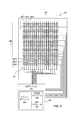
[0040]図2は、処理システム110に結合された複数のセンサ電極(すなわち、送信器電極360及び受信器電極370)を備える入力装置100の概略平面図である。図2では、処理システム110は、受信器電極370と結合され、受信器電極370から結果として生じた信号を受信するように構成されている。また、処理システム110は、送信器電極360と結合され、感知領域120における入力物体を感知することが可能な方法で送信器電極360を動作させるようにも構成されている。
[0040] FIG. 2 is a schematic plan view of the
[0041]図2に示す実施形態において、感知電極は、単純な矩形のパターンに配置されている。一実施形態において、図示するように、感知素子のパターンは、複数の送信器電極360(例えば、送信器電極360−1、360−2、360−3など)、及び複数の送信器電極360上に配置される複数の受信器電極370(例えば、受信器電極370−1、370−2、370−3など)を備える。様々な他の実施形態において、複数の送信器電極360及び複数の受信器電極370は、基板の同じ側に配置されてもよい。さらに、複数の送信器電極360及び複数の受信器電極370が矩形として示されているが、他の実施形態において、センサ電極は、様々な他の形状及びサイズを有することができる。さらに、様々な実施形態において、複数の送信器電極360及び複数の受信器電極370は、サイズ又は形状の少なくとも1つが異なってもよい。さらに他の実施形態において、複数の送信器電極360及び複数の受信器電極370は、同様のサイズであってもよい。別の実施形態において、複数の送信器電極360のうちの少なくとも1つの送信器電極は、複数の送信器電極360のうちの少なくとも第2の送信器電極に対してサイズ及び形状の少なくとも1つが異なる。別の実施形態において、複数の受信器電極370のうちの少なくとも1つの受信器電極は、複数の受信器電極360のうちの少なくとも第2の受信器電極に対してサイズ及び形状の少なくとも1つが異なる。
[0041] In the embodiment shown in FIG. 2, the sensing electrodes are arranged in a simple rectangular pattern. In one embodiment, as illustrated, the pattern of sensing elements is formed on a plurality of transmitter electrodes 360 (eg, transmitter electrodes 360-1, 360-2, 360-3, etc.) and a plurality of
[0042]送信器電極360及び受信器電極370は、典型的には互いにオーミック絶縁されている。すなわち、1つ又は複数の絶縁体が送信器電極360及び受信器電極370を分離し、それらが互いに電気的に短絡しないようにする。一部の実施形態において、送信器電極360及び受信器電極370は、交差領域においてそれらの間に配置された電気的な絶縁材料によって分離される。そうした構成において、送信器電極360及び/又は受信器電極370は、同じ電極の異なる部分をジャンパー接続して形成されてもよい。一部の実施形態において、送信器電極360及び受信器電極370は、電気的な絶縁材料の1つ又は複数の層によって分離される。他の一部の実施形態において、送信器電極360及び受信器電極370は、1つ又は複数の基板によって分離され、例えば、それらは、同じ基板(例えば、カラーフィルタガラス)の両側に、又は互いに積層されている異なる基板に配置されてもよい。他の実施形態において、送信器電極360及び受信器電極370は、単一の層に配置され、それにより、それらは、基板の同様の側に配置される。
[0042] The
[0043]送信器電極360と受信器電極370との間の局所的な容量結合の領域は、「容量性ピクセル」と名付けられることがある。送信器電極360と受信器電極370との間の容量結合は、送信器電極360及び受信器電極370に関連付けられた感知領域120における入力物体140の接近及び動きと共に変化する。
[0043] The region of local capacitive coupling between the
[0044]一部の実施形態において、センサパターンは、これらの容量結合を求めるために「走査」される。すなわち、送信器電極360を駆動して送信器信号を送信する。送信器電極360は、一回につき1つの送信器電極が送信する、又は複数の送信器電極が同時に送信するように動作してもよい。複数の送信器電極が同時に送信する場合、これらの複数の送信器電極は、同じ送信器信号を送信し、実効的により大きな送信器電極を実効的に生成することができ、又はこれらの複数の送信器電極は、異なる送信器信号を送信してもよい。例えば、複数の送信器電極は、1つ又は複数のコーディングスキームにより異なる送信器信号を送信することができ、このコーディングスキームによって、受信器電極370の結果として生じた信号に対する、複数の送信器電極の複合的な影響を個別に求めることができる。受信器センサ電極370は、結果として生じた信号を取得するために単独で又は複合的に動作してもよい。結果として生じた信号は、容量性ピクセルにおける容量結合の測定値を求めるために処理システム110によって使用されてもよく、この測定値を用いて、上で論じたように、入力物体が存在するかどうかを判断し、その位置情報を求める。
[0044] In some embodiments, sensor patterns are "scanned" to determine their capacitive coupling. That is, the
[0045]一部の入力装置の実施形態において、送信器電極360及び/又は受信器電極370は、関連付けられた表示画面の基板に配置される。例えば、送信器電極360及び/又は受信器電極370は、偏光子、カラーフィルタ基板、又はLCDのガラスシートに配置されてもよい。具体的な例として、送信器電極360は、LCDのTFT(薄膜トランジスタ)基板に配置されてもよく、表示画面の表示動作において使用されても、また使用されなくてもよい。別の例として、受信器電極370は、LCDガラスシート上のカラーフィルタ基板、LCDガラスシート一面に配置された保護材料、レンズガラスなどに配置されてもよい。
[0045] In some input device embodiments, the
[0046]処理システム110は、ドライバモジュール404、受信器モジュール406、及び決定モジュール408を備える。一実施形態において、処理システム110は、送信器電極360及び受信器電極370に結合される。
[0046] The
[0047]ドライバモジュール404は、1つ又は複数の電位を有する送信器電極を駆動するように構成されたソフトウェア及び/又はハードウェア(例えば、ドライバ回路)の任意の組み合わせを含む。ドライバモジュール404は、任意の適切な方法で送信器電極360を動作させるように構成されてもよく、それらの例について本明細書で説明する。例えば、ドライバモジュール404は、送信器電極を駆動する、送信器信号を送信する、送信器電極を基準電位に(例えば、V−com電位、システムグランドなどに)保持する、又は送信器電極を高インピーダンスに保持するように構成されてもよい。一部の実施形態において、ドライバモジュール404は、1つ又は複数の送信器電極360を第1の電位から第2の電位に駆動する。代替の実施形態において、追加の電位源は、送信器電極360を送信器電極360の第1の電位と第2の電位との間にある中間電位に駆動する。次いで、ドライバモジュール404は、送信器電極360を中間電位から第2の電位に駆動する。
[0047] The
[0048]受信器モジュール406は、受信器電極を用いて、結果として生じた1つ又は複数の信号を受信するように構成されたソフトウェア及び/又はハードウェアの任意の組み合わせを含む。一実施形態において、受信器モジュール406は、受信器電極370を用いて、結果として生じた信号を受信するように構成される。一部の構成において、受信器モジュール406は、環境上の妨害の量を求めるために、複数の送信器電極360によって送信器信号が送信されていないときに、信号を取得及び/又は受信するように構成される。
[0048] The
[0049]決定モジュール408は、受信器モジュール406によって受信される、結果として生じた信号(複数可)に基づいて、感知領域120の少なくとも1つの入力物体の位置情報を求めるように構成されたハードウェア及び/又はソフトウェアの任意の組み合わせを含む。
[0049] The
[0050]図3は、ドライバモジュール404及び電子蓄積装置502が、本明細書に記載された1つ又は複数の実施形態による、送信器電極の1つ360−1に結合された概略図を示す。一実施形態において、ドライバモジュール404は、第1の送信器電極に結合され、第1の送信器電極を中間電位から第2の電位に駆動するように構成される。ドライバモジュール404は、第1の送信器電極を中間電位から第1の電位に駆動するようにさらに構成されてもよい。電子蓄積装置502は、送信器電極に結合され、送信器電極を第1の電位と第2の電位との間の中間電位に駆動するように構成される。一実施形態において、中間電圧は、システムグランド、V−com、又は入力装置100の基準電圧であってもよい。
[0050] FIG. 3 shows a schematic diagram in which a
[0051]図4の実施形態において、電子蓄積装置502は、コンデンサ508を備え、電子蓄積装置502及びドライバモジュール404は、送信器電極に選択的に結合される。一実施形態において、スイッチングメカニズム506は、ドライバモジュール404及び電子蓄積装置502のコンデンサ508を送信器電極に選択的に結合するように構成される。
[0051] In the embodiment of FIG. 4, the
[0052]一実施形態において、ドライバモジュール404は、電位源に結合されたレギュレータを備える。代替の実施形態において、ドライバモジュール404は、電位源に結合された(例えば、DAC制御された)アンプ又はバッファを備える。さらなる実施形態において、ドライバモジュール404は、電源、電圧ブースト、若しくはインバータ、及び/又はバッファアンプを備える。当業者は、ドライバモジュール404が送信器電極360−1を駆動するように構成された任意のその他のドライバ回路を備えてもよいことを認識するであろう。コンデンサ508は、例えば、ドライバモジュール404又は他の電荷源によって所定の電荷に充電されるように構成される。さらに、コンデンサ508は、送信器電極360を、送信器電極360の第1の電位と第2の電位との間にある中間電位に駆動するように構成される。スイッチングメカニズム506は、ある状態では、送信器電極360−1をコンデンサ508と結合し、別の状態では、送信器電極360−1をドライバモジュール502と結合するように構成される。一実施形態において、スイッチングメカニズム506は、複数のスイッチを備える。別の実施形態において、スイッチングメカニズムは、少なくとも1つの送信器を備える。
[0052] In one embodiment, the
[0053]動作において、送信器電極360−1が第1の電位から第2の電位に駆動されることになる場合、スイッチングメカニズム506は、まず送信器電極360−1をコンデンサ508と結合する。次いで、コンデンサ508が放電して、送信器電極360を第1の電位から第1の電位360と第2の電位との間にある中間電位に駆動する。次に、スイッチングメカニズム506は、送信器電極360−1をドライバモジュール404と結合する。次いで、ドライバモジュール404は、送信器電極360−1を中間電位から第2の電位に駆動する。ドライバモジュール404は、コンデンサ508が送信器電極360−1を中間電位に駆動するため、送信器電極360−1を部分的に駆動するだけでよいのが有益である。そうした実施形態において、ドライバモジュール404は、送信器電極360−1を第1の電位から第2の電位までの全範囲を駆動しないため、入力装置100全体にわたって電力が節約される。一実施形態において、中間電位と第1の電位間の電圧差は、中間電位と第2の電位間の電圧差よりも小さい。別の実施形態において、中間電位と第2の電位間の電圧差は、中間電位と第1の電位間の電圧差よりも小さい。別の実施形態において、中間電位と第2の電位間の電圧差は、実質的に中間電位と第1の電位間の電圧差と同じである。
[0053] In operation, when the transmitter electrode 360-1 is to be driven from a first potential to a second potential, the
[0054]送信器電極360−1は、低電位から高電位、又は高電位から低電位に駆動されうる。送信器電極360−1が低電位から高電位に駆動される場合は、コンデンサ508は、送信器電極360−1が低電位から中間電位に駆動されるときに所定の電荷から放電する。送信器電極360−1が高電位から低電位に駆動される場合は、コンデンサ508は、送信器電極360−1が高電位から中間電位に駆動されるときに送信器電極360−1によって充電される。次いで、コンデンサ508の回復された電荷を用いて、送信器電極360−1(又は他の送信器電極360)を低電位から中間電位に戻るように駆動することができ、したがって入力装置100によって利用される電力の総量を保存することができる。
[0054] The transmitter electrode 360-1 may be driven from a low potential to a high potential, or from a high potential to a low potential. When the transmitter electrode 360-1 is driven from a low potential to a high potential, the
[0055]図5は、本明細書に記載された1つ又は複数の実施形態による、送信器電極360−1、360−2に結合された処理システム110の別の構成を示す概略図である。ある実施形態において、処理システム110は、ドライバモジュール404、スイッチングメカニズム606、スイッチングメカニズム608、及び電子蓄積装置502(例えば、コンデンサ610)を含む。
[0055] FIG. 5 is a schematic diagram illustrating another configuration of a
[0056]ドライバモジュール404は、送信器電極360−1を駆動するように、及び送信器電極360−2を駆動するように構成される。一実施形態において、電子蓄積装置502は、第1及び第2の送信器電極を駆動するように、及び所定の電荷に充電されるように構成されたキャパシタンス610(例えば、共有のコンデンサ)を備える。本実施形態において、コンデンサ610は、送信器電極360−1及び送信器電極360−2の両方を中間電位に駆動するように構成される。処理システム110は、ある状態では、送信器電極360−1をコンデンサ610と結合するように、及び別の状態では、送信器電極360−1をドライバモジュール404と結合するように構成されたスイッチングメカニズム606をさらに備えることができる。また、スイッチングメカニズム608は、ある状態では、送信器電極360−2をコンデンサ610と結合するように、及び別の状態では、送信器電極360−2をドライバモジュール404と結合するように構成される。
[0056] The
[0057]一実施形態において、送信器電極360−1及び送信器電極360−2は、同時に駆動され、その場合送信器電極360−1が高電位から低電位に駆動され、送信器電極360−2が低電位から高電位に駆動される。動作において、スイッチングメカニズム606は、送信器電極360−1をコンデンサ610と結合する。送信器電極360−1からの電荷は、コンデンサ610を中間電位に充電し、したがって、送信器電極360−1を高電位から中間電位に駆動する。次いで、スイッチングメカニズム606は、送信器電極360−1をドライバモジュール404に結合し、このドライバモジュール404が送信器電極360−1を中間電位から低電位に駆動する。コンデンサ610は、送信器電極360−2を駆動するために充電される。スイッチングメカニズム608は、同時に、コンデンサ610を送信器電極360−2に結合して、送信器電極360−2を低電位から中間電位に駆動することができる。一旦送信器電極360−2が中間電位に充電されると、スイッチングメカニズム606は、送信器電極360−2をドライバモジュール404と結合する。次いで、ドライバモジュール404は、送信器電極360−2を中間電位から高電位に駆動する。再び、コンデンサ610が送信器電極360−1及び送信器電極360−2を中間電位に駆動するため、ドライバモジュール404は、送信器電極360−1及び送信器電極360−2を部分的に駆動し、それによって、入力装置100の消費電力が低減される。一部の実施形態において、電子蓄積装置502を用いて、送信器電極を中間電圧に一方向にのみ(例えば、高から低に、又は低から高に)遷移させることができる。
[0057] In one embodiment, transmitter electrode 360-1 and transmitter electrode 360-2 are driven simultaneously, in which case transmitter electrode 360-1 is driven from a high potential to a low potential, and transmitter electrode 360- 2 is driven from a low potential to a high potential. In operation, switching mechanism 606 couples transmitter electrode 360-1 with
[0058]また、上記の技法は、3つ以上の送信器電極を同時に駆動するように実施されてもよい。例えば、4つの送信器電極が同時に駆動されてもよく、その場合2つの送信器電極が低電位から高電位に駆動され、2つの送信器電極が高電位から低電位に駆動される。各送信器電極は、まず充電されたコンデンサによって中間電位に駆動され、次いでドライバモジュールによって第2の電位に駆動される。ある実施形態において、コンデンサは、複数の送信器電極に対して共有されてもよい。そうした動作は、典型的には2つの送信器電極を直接駆動するのに必要となる4つの送信器電極に対して同じピーク電流を利用する。その結果、最大半分の電力を節約することができる。 [0058] The above techniques may also be implemented to drive more than two transmitter electrodes simultaneously. For example, four transmitter electrodes may be driven simultaneously, in which case the two transmitter electrodes are driven from a low potential to a high potential and the two transmitter electrodes are driven from a high potential to a low potential. Each transmitter electrode is first driven to an intermediate potential by a charged capacitor and then driven to a second potential by a driver module. In certain embodiments, the capacitor may be shared for multiple transmitter electrodes. Such operation typically utilizes the same peak current for the four transmitter electrodes that are required to drive the two transmitter electrodes directly. As a result, up to half of the power can be saved.
[0059]加えて、上記の技法は、奇数の送信器電極を用いて実施されてもよい。そうした実施態様においては、送信器電極を遷移させるために比較的大きなコンデンサ(例えば、外部コンデンサ)及び/又はより長い期間(例えば、フレーム)が使用されてもよく、それによりコンデンサの電位が比較的一定に保たれる。 [0059] In addition, the above technique may be implemented with an odd number of transmitter electrodes. In such an embodiment, a relatively large capacitor (eg, an external capacitor) and / or a longer period (eg, a frame) may be used to transition the transmitter electrode so that the capacitor potential is relatively low. Kept constant.
[0060]図6は、本明細書に記載された1つ又は複数の実施形態による、送信器電極360−1、360−2に結合されたドライバモジュール404のさらに別の構成を示す概略図である。図示するように、処理システム110は、ドライバモジュール404、スイッチングメカニズム706、スイッチングメカニズム708、及び短絡板710を含む。本実施形態において、電子蓄積装置502は、送信器電極360を備える。特に、送信器電極360−1に存在する電荷が送信器電極360−2に放電され、又はその逆が行われ、それにより、送信器電極360−1、360−2が、送信器電極に以前存在していた高電位と低電位との間にある中間電位を取得する。
[0060] FIG. 6 is a schematic diagram illustrating yet another configuration of
[0061]動作において、スイッチングメカニズム706及びスイッチングメカニズム708は、短絡板710によって送信器電極360−1及び送信器電極360−2を互いに同時に結合する。送信器電極360−1が高電位に充電されている場合、送信器電極360−1の電荷の一部は、短絡板710を通って送信器電極360−2に流れ、送信器電極360−2を中間電位に充電する。スイッチングメカニズム706は、続いてドライバモジュール404を送信器電極360−1に結合する。次いで、ドライバモジュール404は、送信器電極360−1を中間電位から低電位に駆動する。また、スイッチングメカニズム708は、ドライバモジュール404を送信器電極360−2に結合する。次いで、ドライバモジュール404は、送信器電極360−2を中間電位から高電位に駆動する。同様に、送信器電極360−2が高電位に充電され、送信器電極360−1が低電位に充電されている場合、送信器電極360−2の電荷の一部は、短絡板710を使用して送信器電極360−1に送られ、送信器電極360−1及び360−2を中間電位に充電する。スイッチングメカニズム706は、続いてドライバモジュール404を送信器電極360−1に結合する。次いで、ドライバモジュール404は、送信器電極360−1を中間電位から高電位に駆動する。また、スイッチングメカニズム708は、ドライバモジュール404を送信器電極360−2に結合する。次いで、ドライバモジュール404は、送信器電極360−2を中間電位から低電位に駆動する。
[0061] In operation,
[0062]図7は、本発明の一実施形態による、送信器電極を指定された電位に駆動する例示的な方法700を示す流れ図である。本方法ステップは、図1〜6のシステムに関連して記載されているが、当業者は、任意の順番で、又は他の構成で配置された送信器電極を用いて本方法ステップを行なうように構成されたいかなるシステムも本発明の範囲内にあることを理解するであろう。
[0062] FIG. 7 is a flow diagram illustrating an
[0063]方法700は、ステップ702で始まり、電子蓄積装置は、特定のセンサ電極、例えば送信器電極360−1を中間電位に駆動する。中間電位は、送信器電極の第1の電位と送信器電極の第2の電位との間に入る電位である。第1の電位は、低電位又は高電位であってもよい。第1の電位が低電位の場合、第2の電位は、相対的により高い電位であってもよい。同様に、第1の電位が高電位の場合、第2の電位は、相対的により低い電位であってもよい。一部の実施形態において、電子蓄積装置は、コンデンサである。代替の実施形態において、電子蓄積装置は、別の送信器電極、例えば送信器電極360−2である。ステップ704で、ドライバモジュールは、センサ電極を中間電位から第2の電位に駆動する。
[0063]
[0064]図8は、本発明の一実施形態による、図2のドライバモジュール404の構成を示す概略図である。ドライバモジュール404は、液晶ディスプレイ(LCD)と共に使用されてもよい。様々な実施形態によると、電子蓄積装置502(例えば、コンデンサC2 802)は、送信器電極360−1を第1の電位と第2の電位との間にある中間電位に駆動するために送信器電極360−1に結合される。一実施形態において、中間電圧は、システムグランドである。さらに、第1の電圧は、ディスプレイの共通電極のV−com電圧(例えば、−0.5V)であり、第2の電圧は、正の電源電圧(例えば、5V)である。
[0064] FIG. 8 is a schematic diagram illustrating the configuration of the
[0065]動作において、システムグランドのキャパシタンス(例えば、C1、C2、C3)は、システムグランドが送信器電極360−1に結合されるときに、充電又は放電して送信器電極360−1をシステムグランド電圧に駆動する。ドライバモジュール404は、送信器電極360−1を正の電源電圧に駆動する。その後、送信器電極360−1は、システムグランドに結合され、それによって送信器電極360−1をシステムグランドに駆動する。次いで、ドライバモジュール404は、送信器電極360−1をV−com電圧までの残りの範囲を駆動する。
[0065] In operation, the system ground capacitance (eg, C1, C2, C3) charges or discharges the system when the system ground is coupled to the transmitter electrode 360-1. Drive to ground voltage. The
[0066]このように、V−comを供給するドライバモジュールは、電源804(例えば、電池)からの電荷の供給を少なくし、電力の消費を少なくすることができる。システムグランドのキャパシタンスの充電及び放電は、電力を消費しないことに留意されたい。しかし、送信器電極360−1を正の電源電圧及びV−com電圧に駆動するとき、電力が消費される。中間電圧を提供するシステムグランドを使用することによって、わざわざ電源804からの電荷を使用して送信器電極360−1を駆動する必要がない。したがって、送信器電極360−1を駆動するのに必要な電力が低減される。
[0066] Thus, a driver module that supplies V-com can reduce the supply of charge from a power source 804 (eg, a battery) and reduce power consumption. Note that charging and discharging the system ground capacitance does not consume power. However, power is consumed when the transmitter electrode 360-1 is driven to a positive power supply voltage and V-com voltage. By using a system ground that provides an intermediate voltage, it is not necessary to use the charge from the
[0067]電子蓄積装置を使用して送信器電極を充電し、それによりドライバモジュールが続いて送信器電極を駆動することによって、結果として入力装置全体にわたって電力が節約されるのが有利である。そうした電力の節約は、特に入力装置が限られた電源によって電力が供給されている場合は、極めて有益である。 [0067] Advantageously, the electronic storage device is used to charge the transmitter electrode so that the driver module subsequently drives the transmitter electrode, resulting in power savings across the input device. Such power savings are extremely beneficial, especially when the input device is powered by a limited power source.
[0068]したがって、本明細書に述べた実施形態及び例は、本発明及びその特定の用途について最善の説明を行い、それによって当業者が本発明を行い使用することができるように提示された。しかし、当業者は、前述の記載及び例が単に説明及び例のために提示されたことを認識するであろう。記載された説明は、網羅的であること、又は開示された精密な形態に本発明を限定することは意図されていない。 [0068] Accordingly, the embodiments and examples described herein have been presented to provide the best description of the invention and its particular applications, thereby enabling those skilled in the art to make and use the invention. . However, one of ordinary skill in the art will recognize that the foregoing description and examples have been presented for purposes of illustration and example only. The description as set forth is not intended to be exhaustive or to limit the invention to the precise form disclosed.
[0069]上記は、本発明の実施形態を対象としているが、本発明の他の及びさらなる実施形態が本発明の基本的な範囲から逸脱せずに考案されてもよく、本発明の範囲は、以下の特許請求の範囲によって決定される。
[発明の項目]
[項目1]
入力装置の処理システムであって、
第1の電位と第2の電位との間で駆動されたときに第1の送信器信号を発するように構成された第1の送信器電極に結合された、ドライバ回路を備えるドライバモジュールであって、前記第1の送信器電極を中間電位から前記第2の電位に駆動するように構成され、前記中間電位が前記第1の電位と前記第2の電位との間にあり、前記第1の送信器電極が、前記第1の送信器電極を前記中間電位に駆動するように構成された電子蓄積装置にさらに結合される、ドライバモジュールと、
受信器電極に結合され、前記受信器電極を用いて、結果として生じた信号を受信するように構成された受信器モジュールであって、前記結果として生じた信号が前記第1の送信器信号に対応する影響を含む、受信器モジュールと、
前記結果として生じた信号に基づいて前記入力装置の感知領域における入力物体の位置情報を求めるように構成された決定モジュールと
を備える、処理システム。
[項目2]
前記ドライバモジュール及び前記電子蓄積装置を前記第1の送信器電極に選択的に結合するように構成される、項目1に記載の処理システム。
[項目3]
前記中間電圧が実質的にシステムグランド電圧である、項目1に記載の処理システム。
[項目4]
前記電子蓄積装置がコンデンサを備える、項目1に記載の処理システム。
[項目5]
前記コンデンサが、第2の送信器電極に選択的に結合されるように構成され、前記第2の送信器電極が、前記第1の電位と前記第2の電位との間で駆動されたときに第2の送信器信号を発するように構成され、前記受信器モジュールが前記受信器電極を用いて、前記第2の送信器信号の影響を含む結果として生じた第2の信号を受信するようにさらに構成され、前記決定モジュールが、前記結果として生じた第2の信号に基づいて前記入力装置の前記感知領域における前記入力物体の位置情報を求めるようにさらに構成される、項目4に記載の処理システム。
[項目6]
前記コンデンサが、前記第1の送信器電極を前記第1の電圧から前記中間電圧に駆動するように構成され、前記第2の送信器電極を前記第2の電圧から前記中間電圧に駆動するように構成される、項目5に記載の処理システム。
[項目7]
前記電子蓄積装置が、第2の送信器信号を発するように構成される第2の送信器電極を備え、前記第1の送信器電極を前記中間電位に駆動することが、前記第1の送信器電極を前記第2の送信器電極と結合することを含む、項目1に記載の処理システム。
[項目8]
前記電子蓄積装置が、前記第1の送信器電極を前記第1の電圧から前記中間電圧に駆動するように構成され、前記中間電圧が前記第1の電圧よりも高い、項目1に記載の処理システム。
[項目9]
前記電子蓄積装置が、前記第1の送信器電極を前記第2の電圧から前記中間電圧に駆動するように構成され、前記中間電圧が前記第2の電圧よりも低い、項目1に記載の処理システム。
[項目10]
入力装置であって、
第1の電位と第2の電位との間で駆動されたときに第1の送信器信号を発するように構成された第1の送信器電極を備える複数の送信器電極と、
第1の受信器電極を備える複数の受信器電極と、
前記第1の送信器電極に結合され、前記第1の送信器電極を前記第1の電位と第2の電位との間にある中間電位に駆動するように構成された電子蓄積装置と、
前記中間電位と前記第2の電位との間で前記第1の送信器電極を駆動し、前記第1の受信器電極を用いて、前記第1の送信器電極信号に対応する影響を含む、結果として生じた信号を受信し、前記結果として生じた信号に基づいて前記入力装置の感知領域における入力物体の位置情報を求めるように構成された、前記第1の送信器電極及び前記第1の受信器電極に結合された処理システムと
を備える、入力装置。
[項目11]
前記電子蓄積装置を前記第1の送信器電極に結合する第1の状態、及びドライバモジュールを前記第1の送信器電極に結合する第2の状態を有するスイッチングメカニズムをさらに備える、項目10に記載の入力装置。
[項目12]
前記電子蓄積装置がコンデンサを備える、項目10に記載の入力装置。
[項目13]
前記コンデンサが、第2の送信器電極に選択的に結合されるように構成され、前記第2の送信器電極が、前記第1の電位と前記第2の電位との間で駆動されたときに第2の送信器信号を発するように構成され、受信器モジュールが、前記第1の受信器電極を用いて、前記第2の送信器信号の影響を含む結果として生じた第2の信号を受信するようにさらに構成され、決定モジュールが、前記結果として生じた第2の信号に基づいて前記入力装置の前記感知領域における前記入力物体の位置情報を求めるようにさらに構成される、項目12に記載の入力装置。
[項目14]
前記コンデンサが、前記第1の送信器電極を前記第1の電圧から前記中間電圧に駆動するように構成され、前記第2の送信器電極を前記第2の電圧から前記中間電圧に駆動するように構成される、項目13に記載の入力装置。
[項目15]
前記電子蓄積装置が、第2の送信器信号を発するように構成される第2の送信器電極を備え、前記第1の送信器電極を前記中間電位に駆動することが、前記第1の送信器電極を前記第2の送信器電極と結合することを含む、項目10に記載の入力装置。
[項目16]
前記第1の送信器電極を前記第1の電位と第2の電位との間にある中間電位に駆動することが、前記第1の送信器電極を前記第1の電位から第1の電位よりも高い前記中間電位に駆動することであって、前記電子蓄積装置が、第2の送信器電極を前記第2の電位から前記第2の電位よりも低い前記中間電位に駆動するようにさらに構成される、項目10に記載の入力装置。
[項目17]
前記第1の送信器電極を前記第1の電位と第2の電位との間にある中間電位に駆動することが、
前記第1の送信器電極を、前記電子蓄積装置が第1のモードで動作している場合は、前記第1の電位から前記第1の電圧よりも高い前記中間電位に駆動することと、
前記第1の送信器電極を、前記電子蓄積装置が第2のモードで動作している場合は、前記第2の電圧から前記第2の電位よりも低い前記中間電圧に駆動することと
を含む、項目10に記載の入力装置。
[項目18]
入力装置を動作させる方法であって、
第1の電位と第2の電位との間で第1の送信器電極を駆動することによって、前記第1の送信器電極を用いて送信器信号を送信するステップであって、前記第1の電位と前記第2の電位との間で前記第1の送信器電極を駆動するステップが、電子蓄積装置を用いて前記第1の送信器電極を前記第1の電位と第2の電位との間にある中間電位に駆動するステップ及びドライバを用いて前記第1の送信器電極を前記中間電位から前記第2の電位に駆動するステップを含む、前記ステップと、
受信器電極を用いて、前記第1の送信器電極信号に対応する影響を含む、結果として生じた信号を受信するステップと、
前記結果として生じた信号に基づいて前記入力装置の感知領域における入力物体の位置情報を求めるステップと
を含む、方法。
[項目19]
前記電子蓄積装置がコンデンサを備える、項目18に記載の方法。
[項目20]
前記電子蓄積装置が、第2の送信器信号を発するように構成される第2の送信器電極を備え、前記第1の送信器電極を前記中間電位に駆動するステップが、前記第1の送信器電極を前記第2の送信器電極と結合するステップを含む、項目18に記載の方法。
[0069] While the above is directed to embodiments of the invention, other and further embodiments of the invention may be devised without departing from the basic scope thereof, and the scope of the invention is As determined by the following claims.
[Items of Invention]
[Item 1]
An input device processing system,
A driver module comprising a driver circuit coupled to a first transmitter electrode configured to emit a first transmitter signal when driven between a first potential and a second potential. The first transmitter electrode is driven from an intermediate potential to the second potential, the intermediate potential being between the first potential and the second potential; A driver module further coupled to an electronic storage device configured to drive the first transmitter electrode to the intermediate potential;
A receiver module coupled to a receiver electrode and configured to receive the resulting signal using the receiver electrode, wherein the resulting signal is transmitted to the first transmitter signal; A receiver module, including corresponding effects;
A determination module configured to determine position information of an input object in a sensing area of the input device based on the resulting signal;
A processing system comprising:
[Item 2]
The processing system of claim 1, wherein the processing system is configured to selectively couple the driver module and the electronic storage device to the first transmitter electrode.
[Item 3]
Item 2. The processing system of item 1, wherein the intermediate voltage is substantially a system ground voltage.
[Item 4]
The processing system of item 1, wherein the electronic storage device comprises a capacitor.
[Item 5]
The capacitor is configured to be selectively coupled to a second transmitter electrode, and the second transmitter electrode is driven between the first potential and the second potential; And the receiver module uses the receiver electrode to receive the resulting second signal including the effects of the second transmitter signal. Item 5. The item 4, wherein the determination module is further configured to determine position information of the input object in the sensing area of the input device based on the resulting second signal. Processing system.
[Item 6]
The capacitor is configured to drive the first transmitter electrode from the first voltage to the intermediate voltage, and to drive the second transmitter electrode from the second voltage to the intermediate voltage. 6. The processing system according to item 5, which is configured as follows.
[Item 7]
The electronic storage device comprises a second transmitter electrode configured to emit a second transmitter signal, and driving the first transmitter electrode to the intermediate potential includes the first transmission. 2. A processing system according to item 1, comprising coupling a transmitter electrode with the second transmitter electrode.
[Item 8]
The process of item 1, wherein the electronic storage device is configured to drive the first transmitter electrode from the first voltage to the intermediate voltage, the intermediate voltage being higher than the first voltage. system.
[Item 9]
The process of item 1, wherein the electronic storage device is configured to drive the first transmitter electrode from the second voltage to the intermediate voltage, the intermediate voltage being lower than the second voltage. system.
[Item 10]
An input device,
A plurality of transmitter electrodes comprising a first transmitter electrode configured to emit a first transmitter signal when driven between a first potential and a second potential;
A plurality of receiver electrodes comprising a first receiver electrode;
An electronic storage device coupled to the first transmitter electrode and configured to drive the first transmitter electrode to an intermediate potential between the first and second potentials;
Driving the first transmitter electrode between the intermediate potential and the second potential and using the first receiver electrode to include an effect corresponding to the first transmitter electrode signal; Receiving the resulting signal and determining the position information of the input object in the sensing area of the input device based on the resulting signal and the first transmitter electrode and the first A processing system coupled to the receiver electrode;
An input device comprising:
[Item 11]
11. The item 10 further comprising a switching mechanism having a first state coupling the electronic storage device to the first transmitter electrode and a second state coupling a driver module to the first transmitter electrode. Input device.
[Item 12]
Item 11. The input device according to Item 10, wherein the electronic storage device comprises a capacitor.
[Item 13]
The capacitor is configured to be selectively coupled to a second transmitter electrode, and the second transmitter electrode is driven between the first potential and the second potential; A second transmitter signal is generated, and the receiver module uses the first receiver electrode to generate a resulting second signal including the effects of the second transmitter signal. In item 12, further configured to receive and wherein the determination module is further configured to determine position information of the input object in the sensing area of the input device based on the resulting second signal. The input device described.
[Item 14]
The capacitor is configured to drive the first transmitter electrode from the first voltage to the intermediate voltage, and to drive the second transmitter electrode from the second voltage to the intermediate voltage. Item 14. The input device according to Item 13, wherein
[Item 15]
The electronic storage device comprises a second transmitter electrode configured to emit a second transmitter signal, and driving the first transmitter electrode to the intermediate potential includes the first transmission. 12. An input device according to item 10, comprising coupling a transmitter electrode with the second transmitter electrode.
[Item 16]
Driving the first transmitter electrode to an intermediate potential that is between the first and second potentials causes the first transmitter electrode to be driven from the first potential to the first potential. And the electronic storage device is further configured to drive the second transmitter electrode from the second potential to the intermediate potential lower than the second potential. The input device according to item 10, wherein:
[Item 17]
Driving the first transmitter electrode to an intermediate potential between the first and second potentials;
Driving the first transmitter electrode from the first potential to the intermediate potential higher than the first voltage when the electron storage device is operating in a first mode;
Driving the first transmitter electrode from the second voltage to the intermediate voltage lower than the second potential when the electron storage device is operating in the second mode;
The input device according to item 10, comprising:
[Item 18]
A method of operating an input device,
Transmitting a transmitter signal using the first transmitter electrode by driving the first transmitter electrode between a first potential and a second potential, the first potential being Driving the first transmitter electrode between a potential and the second potential using an electronic storage device to connect the first transmitter electrode between the first potential and the second potential; Driving to an intermediate potential in between and driving the first transmitter electrode from the intermediate potential to the second potential using a driver; and
Receiving a resulting signal using a receiver electrode, including an effect corresponding to the first transmitter electrode signal;
Obtaining position information of an input object in a sensing area of the input device based on the resulting signal;
Including a method.
[Item 19]
19. A method according to item 18, wherein the electronic storage device comprises a capacitor.
[Item 20]
The electronic storage device comprises a second transmitter electrode configured to emit a second transmitter signal, and driving the first transmitter electrode to the intermediate potential includes the first transmission. 19. A method according to item 18, comprising the step of coupling a transmitter electrode with the second transmitter electrode.
Claims (7)
第1の電位と第2の電位との間で駆動されたときに第1の送信器信号を発するように構成された第1の送信器電極に結合された、ドライバ回路を備えるドライバモジュールであって、前記第1の送信器電極を前記第1の電位と前記第2の電位との間にある中間電位から前記第2の電位に駆動するように構成され、前記第1の送信器電極が、前記第1の送信器電極を前記中間電位に駆動するように構成された電子蓄積装置にさらに結合される、ドライバモジュールと、
受信器電極に結合され、前記受信器電極を用いて、前記第1の送信器信号に対応する影響を含む結果信号を受信するように構成された受信器モジュールと、
前記結果信号に基づいて前記入力装置の感知領域における入力物体の位置情報を求めるように構成された決定モジュールとを備える、処理システム。 An input device processing system,
A driver module comprising a driver circuit coupled to a first transmitter electrode configured to emit a first transmitter signal when driven between a first potential and a second potential. The first transmitter electrode is configured to be driven from the intermediate potential between the first potential and the second potential to the second potential, and the first transmitter electrode is A driver module further coupled to an electronic storage device configured to drive the first transmitter electrode to the intermediate potential;
A receiver module coupled to a receiver electrode and configured to receive, using the receiver electrode, a result signal including an effect corresponding to the first transmitter signal;
And a determination module configured to determine position information of an input object in a sensing area of the input device based on the result signal.
第1の電位と第2の電位との間で駆動されたときに第1の送信器信号を発するように構成された第1の送信器電極を備える複数の送信器電極と、
第1の受信器電極を備える複数の受信器電極と、
前記第1の送信器電極に結合され、前記第1の送信器電極を前記第1の電位と第2の電位との間にある中間電位に駆動するように構成された電子蓄積装置と、
前記中間電位と前記第2の電位との間で前記第1の送信器電極を駆動し、前記第1の受信器電極を用いて前記第1の送信器信号に対応する影響を含む結果信号を受信し、前記結果信号に基づいて前記入力装置の感知領域における入力物体の位置情報を求めるように構成された、前記第1の送信器電極及び前記第1の受信器電極に結合された処理システムとを備える、入力装置。 An input device,
A plurality of transmitter electrodes comprising a first transmitter electrode configured to emit a first transmitter signal when driven between a first potential and a second potential;
A plurality of receiver electrodes comprising a first receiver electrode;
An electronic storage device coupled to the first transmitter electrode and configured to drive the first transmitter electrode to an intermediate potential between the first and second potentials;
Wherein driving the first transmitter electrode between the intermediate potential and said second potential, the first result signal including the effect corresponding to No. of the first transmission Utsuwashin using receiver electrodes And coupled to the first transmitter electrode and the first receiver electrode configured to determine position information of an input object in a sensing area of the input device based on the result signal An input device comprising the system.
第1の電位と第2の電位との間で第1の送信器電極を駆動することによって、前記第1の送信器電極を用いて送信器信号を送信するステップであって、前記第1の電位と前記第2の電位との間で前記第1の送信器電極を駆動するステップが、第2のセンサ電極を用いて前記第1の送信器電極を前記第1の電位と第2の電位との間にある中間電位に駆動するステップ及びドライバを用いて前記第1の送信器電極を前記中間電位から前記第2の電位に駆動するステップを含む、前記ステップと、
受信器電極を用いて前記送信器信号に対応する影響を含む結果信号を受信するステップとを含む、方法。 A method of operating an input device,
Transmitting a transmitter signal using the first transmitter electrode by driving the first transmitter electrode between a first potential and a second potential, the first potential being Driving the first transmitter electrode between a potential and the second potential using a second sensor electrode to connect the first transmitter electrode to the first potential and the second potential; Driving the first transmitter electrode from the intermediate potential to the second potential using a driver and driving the intermediate potential between the intermediate potential, and
Before using the receiver electrodes and receiving the result signal including the effect corresponding to No. Kioku signal Utsuwashin method.
Applications Claiming Priority (3)
| Application Number | Priority Date | Filing Date | Title |
|---|---|---|---|
| US13/434,463 US9927891B2 (en) | 2012-03-29 | 2012-03-29 | System and method for reducing transmitter power consumption |
| US13/434,463 | 2012-03-29 | ||
| PCT/US2013/029694 WO2013148104A1 (en) | 2012-03-29 | 2013-03-07 | System and method for reducing transmitter power consumption |
Publications (3)
| Publication Number | Publication Date |
|---|---|
| JP2015515681A JP2015515681A (en) | 2015-05-28 |
| JP2015515681A5 JP2015515681A5 (en) | 2016-04-21 |
| JP6156886B2 true JP6156886B2 (en) | 2017-07-05 |
Family
ID=49234231
Family Applications (1)
| Application Number | Title | Priority Date | Filing Date |
|---|---|---|---|
| JP2015503232A Active JP6156886B2 (en) | 2012-03-29 | 2013-03-07 | System and method for reducing transmitter power consumption |
Country Status (5)
| Country | Link |
|---|---|
| US (1) | US9927891B2 (en) |
| JP (1) | JP6156886B2 (en) |
| KR (1) | KR102146585B1 (en) |
| CN (1) | CN104185828B (en) |
| WO (1) | WO2013148104A1 (en) |
Cited By (1)
| Publication number | Priority date | Publication date | Assignee | Title |
|---|---|---|---|---|
| WO2023085014A1 (en) * | 2021-11-11 | 2023-05-19 | 株式会社ワコム | Sensor controller, electronic apparatus, and method for controlling sensor controller |
Families Citing this family (6)
| Publication number | Priority date | Publication date | Assignee | Title |
|---|---|---|---|---|
| US8970546B2 (en) | 2012-08-31 | 2015-03-03 | Synaptics Incorporated | Method and apparatus for improved input sensing using a display processor reference signal |
| US10108292B2 (en) * | 2015-04-22 | 2018-10-23 | Microchip Technology Incorporated | Capacitive sensor system with multiple transmit electrodes |
| US9715297B2 (en) * | 2015-06-30 | 2017-07-25 | Synaptics Incorporated | Flexible display and touch driver IC architecture |
| US9983246B2 (en) * | 2016-01-15 | 2018-05-29 | Cypress Semiconductor Corporation | Quasi-differential mutual capacitance measurement |
| KR102599075B1 (en) * | 2019-05-28 | 2023-11-07 | 주식회사 엘엑스세미콘 | Apparatus and system for sensing touch or proximity of an external object |
| WO2023037690A1 (en) * | 2021-09-13 | 2023-03-16 | 株式会社ワコム | Sensor controller, electronic apparatus, and method for controlling sensor controller |
Family Cites Families (21)
| Publication number | Priority date | Publication date | Assignee | Title |
|---|---|---|---|---|
| WO1998028731A2 (en) | 1996-12-20 | 1998-07-02 | Cirrus Logic, Inc. | Liquid crystal display signal driver system and method |
| JP3613246B2 (en) | 2002-02-08 | 2005-01-26 | セイコーエプソン株式会社 | Display device, driving method thereof, and electronic apparatus |
| JP3820379B2 (en) | 2002-03-13 | 2006-09-13 | 松下電器産業株式会社 | Liquid crystal drive device |
| JP3799308B2 (en) | 2002-08-02 | 2006-07-19 | Nec液晶テクノロジー株式会社 | Liquid crystal display |
| JP4421559B2 (en) * | 2003-01-08 | 2010-02-24 | 東芝モバイルディスプレイ株式会社 | Liquid crystal display |
| JP3861860B2 (en) | 2003-07-18 | 2006-12-27 | セイコーエプソン株式会社 | Power supply circuit, display driver, and voltage supply method |
| TWI258724B (en) | 2003-10-28 | 2006-07-21 | Samsung Electronics Co Ltd | Circuits and methods providing reduced power consumption for driving flat panel displays |
| US7864160B2 (en) | 2005-10-05 | 2011-01-04 | 3M Innovative Properties Company | Interleaved electrodes for touch sensing |
| DE202007005237U1 (en) | 2006-04-25 | 2007-07-05 | Philipp, Harald, Southampton | Touch-sensitive position sensor for use in control panel, has bus bars arranged at distance to substrate, and detection region with units that are arranged at distance by non-conductive openings such that current flows into region |
| US7450422B2 (en) * | 2006-05-11 | 2008-11-11 | Micron Technology, Inc. | NAND architecture memory devices and operation |
| JP4872113B2 (en) * | 2007-09-10 | 2012-02-08 | 株式会社ワコム | Position detection device |
| US8358142B2 (en) | 2008-02-27 | 2013-01-22 | Cypress Semiconductor Corporation | Methods and circuits for measuring mutual and self capacitance |
| WO2009140347A2 (en) | 2008-05-14 | 2009-11-19 | 3M Innovative Properties Company | Systems and methods for assessing locations of multiple touch inputs |
| JP4768039B2 (en) | 2009-03-02 | 2011-09-07 | パナソニック株式会社 | Display drive device and display device |
| US9804213B2 (en) | 2009-05-13 | 2017-10-31 | Synaptics Incorporated | Capacitive sensor device |
| JP5439060B2 (en) | 2009-06-30 | 2014-03-12 | 株式会社ジャパンディスプレイ | Display device |
| JP2011243081A (en) * | 2010-05-20 | 2011-12-01 | Panasonic Corp | Touch panel device |
| JP2012022543A (en) | 2010-07-15 | 2012-02-02 | Panasonic Corp | Touch panel system |
| TWI436248B (en) * | 2011-01-04 | 2014-05-01 | Raydium Semiconductor Corp | Touch sensing apparatus |
| TW201306005A (en) * | 2011-07-22 | 2013-02-01 | Novatek Microelectronics Corp | Method and apparatus for driving a display device with charge sharing |
| US8878758B2 (en) * | 2011-07-29 | 2014-11-04 | Stmicroelectronics S.R.L. | Charge-sharing path control device for a scan driver of an LCD panel |
-
2012
- 2012-03-29 US US13/434,463 patent/US9927891B2/en active Active
-
2013
- 2013-03-07 WO PCT/US2013/029694 patent/WO2013148104A1/en active Application Filing
- 2013-03-07 CN CN201380016859.5A patent/CN104185828B/en active Active
- 2013-03-07 JP JP2015503232A patent/JP6156886B2/en active Active
- 2013-03-07 KR KR1020147030194A patent/KR102146585B1/en active IP Right Grant
Cited By (1)
| Publication number | Priority date | Publication date | Assignee | Title |
|---|---|---|---|---|
| WO2023085014A1 (en) * | 2021-11-11 | 2023-05-19 | 株式会社ワコム | Sensor controller, electronic apparatus, and method for controlling sensor controller |
Also Published As
| Publication number | Publication date |
|---|---|
| US9927891B2 (en) | 2018-03-27 |
| US20130257745A1 (en) | 2013-10-03 |
| WO2013148104A1 (en) | 2013-10-03 |
| CN104185828B (en) | 2017-05-17 |
| CN104185828A (en) | 2014-12-03 |
| KR20140144248A (en) | 2014-12-18 |
| JP2015515681A (en) | 2015-05-28 |
| KR102146585B1 (en) | 2020-08-21 |
Similar Documents
| Publication | Publication Date | Title |
|---|---|---|
| US8902191B2 (en) | Proximity sensing for capacitive touch sensors | |
| KR102265245B1 (en) | Display guarding techniques | |
| JP6336604B2 (en) | Modulated power supply for reducing parasitic capacitance | |
| US9075488B2 (en) | Virtual geometries for integrated display and sensing devices | |
| JP6156886B2 (en) | System and method for reducing transmitter power consumption | |
| US9946404B1 (en) | LED screen noise sensing for discreet capacitive sensors | |
| US10095948B2 (en) | Modulation scheme for fingerprint sensing | |
| US20160183382A1 (en) | Capacitive image sensor with selectable function electrodes | |
| US9652060B2 (en) | Low-latency touch feedback | |
| US9285934B2 (en) | Shielding with display elements | |
| KR102362638B1 (en) | Routing for an integrated display and input sensing device | |
| US10175827B2 (en) | Detecting an active pen using a capacitive sensing device | |
| US20190339809A1 (en) | Transcapacitive touch and force sensing in an input device | |
| US9785296B2 (en) | Force enhanced input device with shielded electrodes | |
| US9280233B1 (en) | Routing for touch sensor electrodes | |
| US20210157434A1 (en) | Device and method for proximity sensing on an input device | |
| US10037112B2 (en) | Sensing an active device'S transmission using timing interleaved with display updates | |
| US9715312B2 (en) | Input device having anti-static layer bypass | |
| US9459367B2 (en) | Capacitive sensor driving technique that enables hybrid sensing or equalization | |
| CN107544708B (en) | Selective receiver electrode scanning | |
| CN105760027B (en) | Switched capacitor technology for input sensing | |
| US9870105B2 (en) | Far-field sensing with a display device having an integrated sensing device | |
| US10540027B2 (en) | Force sensing in a touch display | |
| US10338740B2 (en) | Reducing background capacitance associated with a touch surface |
Legal Events
| Date | Code | Title | Description |
|---|---|---|---|
| A521 | Request for written amendment filed |
Free format text: JAPANESE INTERMEDIATE CODE: A523 Effective date: 20160302 |
|
| A621 | Written request for application examination |
Free format text: JAPANESE INTERMEDIATE CODE: A621 Effective date: 20160302 |
|
| A977 | Report on retrieval |
Free format text: JAPANESE INTERMEDIATE CODE: A971007 Effective date: 20161227 |
|
| A131 | Notification of reasons for refusal |
Free format text: JAPANESE INTERMEDIATE CODE: A131 Effective date: 20170131 |
|
| A521 | Request for written amendment filed |
Free format text: JAPANESE INTERMEDIATE CODE: A523 Effective date: 20170418 |
|
| TRDD | Decision of grant or rejection written | ||
| A01 | Written decision to grant a patent or to grant a registration (utility model) |
Free format text: JAPANESE INTERMEDIATE CODE: A01 Effective date: 20170509 |
|
| A61 | First payment of annual fees (during grant procedure) |
Free format text: JAPANESE INTERMEDIATE CODE: A61 Effective date: 20170601 |
|
| R150 | Certificate of patent or registration of utility model |
Ref document number: 6156886 Country of ref document: JP Free format text: JAPANESE INTERMEDIATE CODE: R150 |
|
| R250 | Receipt of annual fees |
Free format text: JAPANESE INTERMEDIATE CODE: R250 |
|
| R250 | Receipt of annual fees |
Free format text: JAPANESE INTERMEDIATE CODE: R250 |
|
| R250 | Receipt of annual fees |
Free format text: JAPANESE INTERMEDIATE CODE: R250 |
|
| R250 | Receipt of annual fees |
Free format text: JAPANESE INTERMEDIATE CODE: R250 |