JP6155997B2 - Power storage device and method for manufacturing power storage device - Google Patents
Power storage device and method for manufacturing power storage device Download PDFInfo
- Publication number
- JP6155997B2 JP6155997B2 JP2013189084A JP2013189084A JP6155997B2 JP 6155997 B2 JP6155997 B2 JP 6155997B2 JP 2013189084 A JP2013189084 A JP 2013189084A JP 2013189084 A JP2013189084 A JP 2013189084A JP 6155997 B2 JP6155997 B2 JP 6155997B2
- Authority
- JP
- Japan
- Prior art keywords
- lead
- current collector
- joined
- lead portion
- axis direction
- Prior art date
- Legal status (The legal status is an assumption and is not a legal conclusion. Google has not performed a legal analysis and makes no representation as to the accuracy of the status listed.)
- Expired - Fee Related
Links
- 238000003860 storage Methods 0.000 title claims description 41
- 238000000034 method Methods 0.000 title claims description 9
- 238000004519 manufacturing process Methods 0.000 title claims description 6
- 238000005192 partition Methods 0.000 claims description 72
- 238000004804 winding Methods 0.000 claims description 51
- 229910052751 metal Inorganic materials 0.000 claims description 49
- 239000002184 metal Substances 0.000 claims description 49
- 239000011888 foil Substances 0.000 claims description 19
- 230000002093 peripheral effect Effects 0.000 claims description 18
- 238000005304 joining Methods 0.000 claims description 11
- 230000005611 electricity Effects 0.000 claims description 7
- 238000003825 pressing Methods 0.000 claims description 4
- 230000000630 rising effect Effects 0.000 claims description 3
- 239000000843 powder Substances 0.000 description 23
- 238000003466 welding Methods 0.000 description 11
- 238000005452 bending Methods 0.000 description 8
- 239000000463 material Substances 0.000 description 7
- 238000012856 packing Methods 0.000 description 6
- RYGMFSIKBFXOCR-UHFFFAOYSA-N Copper Chemical compound [Cu] RYGMFSIKBFXOCR-UHFFFAOYSA-N 0.000 description 5
- 239000007788 liquid Substances 0.000 description 5
- 229910052744 lithium Inorganic materials 0.000 description 5
- 239000007773 negative electrode material Substances 0.000 description 5
- 239000007774 positive electrode material Substances 0.000 description 5
- WHXSMMKQMYFTQS-UHFFFAOYSA-N Lithium Chemical compound [Li] WHXSMMKQMYFTQS-UHFFFAOYSA-N 0.000 description 4
- 229910052782 aluminium Inorganic materials 0.000 description 4
- XAGFODPZIPBFFR-UHFFFAOYSA-N aluminium Chemical compound [Al] XAGFODPZIPBFFR-UHFFFAOYSA-N 0.000 description 4
- 230000035515 penetration Effects 0.000 description 4
- HBBGRARXTFLTSG-UHFFFAOYSA-N Lithium ion Chemical compound [Li+] HBBGRARXTFLTSG-UHFFFAOYSA-N 0.000 description 3
- 229910052802 copper Inorganic materials 0.000 description 3
- 239000010949 copper Substances 0.000 description 3
- 238000005520 cutting process Methods 0.000 description 3
- 229910001416 lithium ion Inorganic materials 0.000 description 3
- 239000000203 mixture Substances 0.000 description 3
- PXHVJJICTQNCMI-UHFFFAOYSA-N Nickel Chemical compound [Ni] PXHVJJICTQNCMI-UHFFFAOYSA-N 0.000 description 2
- 239000011149 active material Substances 0.000 description 2
- 239000008151 electrolyte solution Substances 0.000 description 2
- 238000002347 injection Methods 0.000 description 2
- 239000007924 injection Substances 0.000 description 2
- 230000033001 locomotion Effects 0.000 description 2
- 150000002739 metals Chemical class 0.000 description 2
- 238000000465 moulding Methods 0.000 description 2
- 230000001105 regulatory effect Effects 0.000 description 2
- 239000011347 resin Substances 0.000 description 2
- 229920005989 resin Polymers 0.000 description 2
- LIVNPJMFVYWSIS-UHFFFAOYSA-N silicon monoxide Chemical compound [Si-]#[O+] LIVNPJMFVYWSIS-UHFFFAOYSA-N 0.000 description 2
- 229910000838 Al alloy Inorganic materials 0.000 description 1
- OKTJSMMVPCPJKN-UHFFFAOYSA-N Carbon Chemical compound [C] OKTJSMMVPCPJKN-UHFFFAOYSA-N 0.000 description 1
- 229910000733 Li alloy Inorganic materials 0.000 description 1
- 229910012851 LiCoO 2 Inorganic materials 0.000 description 1
- 229910010707 LiFePO 4 Inorganic materials 0.000 description 1
- 229910015643 LiMn 2 O 4 Inorganic materials 0.000 description 1
- 229910013716 LiNi Inorganic materials 0.000 description 1
- 229910013290 LiNiO 2 Inorganic materials 0.000 description 1
- XUIMIQQOPSSXEZ-UHFFFAOYSA-N Silicon Chemical compound [Si] XUIMIQQOPSSXEZ-UHFFFAOYSA-N 0.000 description 1
- 229910000681 Silicon-tin Inorganic materials 0.000 description 1
- ATJFFYVFTNAWJD-UHFFFAOYSA-N Tin Chemical compound [Sn] ATJFFYVFTNAWJD-UHFFFAOYSA-N 0.000 description 1
- RTAQQCXQSZGOHL-UHFFFAOYSA-N Titanium Chemical compound [Ti] RTAQQCXQSZGOHL-UHFFFAOYSA-N 0.000 description 1
- HFCVPDYCRZVZDF-UHFFFAOYSA-N [Li+].[Co+2].[Ni+2].[O-][Mn]([O-])(=O)=O Chemical compound [Li+].[Co+2].[Ni+2].[O-][Mn]([O-])(=O)=O HFCVPDYCRZVZDF-UHFFFAOYSA-N 0.000 description 1
- 239000000654 additive Substances 0.000 description 1
- 239000003990 capacitor Substances 0.000 description 1
- 239000003575 carbonaceous material Substances 0.000 description 1
- 150000001875 compounds Chemical class 0.000 description 1
- QHGJSLXSVXVKHZ-UHFFFAOYSA-N dilithium;dioxido(dioxo)manganese Chemical compound [Li+].[Li+].[O-][Mn]([O-])(=O)=O QHGJSLXSVXVKHZ-UHFFFAOYSA-N 0.000 description 1
- 238000007599 discharging Methods 0.000 description 1
- 239000010439 graphite Substances 0.000 description 1
- 229910002804 graphite Inorganic materials 0.000 description 1
- 230000002687 intercalation Effects 0.000 description 1
- 238000009830 intercalation Methods 0.000 description 1
- 230000009545 invasion Effects 0.000 description 1
- 239000001989 lithium alloy Substances 0.000 description 1
- GELKBWJHTRAYNV-UHFFFAOYSA-K lithium iron phosphate Chemical compound [Li+].[Fe+2].[O-]P([O-])([O-])=O GELKBWJHTRAYNV-UHFFFAOYSA-K 0.000 description 1
- ILXAVRFGLBYNEJ-UHFFFAOYSA-K lithium;manganese(2+);phosphate Chemical compound [Li+].[Mn+2].[O-]P([O-])([O-])=O ILXAVRFGLBYNEJ-UHFFFAOYSA-K 0.000 description 1
- 239000011572 manganese Substances 0.000 description 1
- 229910052759 nickel Inorganic materials 0.000 description 1
- 239000011255 nonaqueous electrolyte Substances 0.000 description 1
- 230000003405 preventing effect Effects 0.000 description 1
- 229910052710 silicon Inorganic materials 0.000 description 1
- 239000010703 silicon Substances 0.000 description 1
- 238000006467 substitution reaction Methods 0.000 description 1
- 229910000314 transition metal oxide Inorganic materials 0.000 description 1
Images


Classifications
-
- Y—GENERAL TAGGING OF NEW TECHNOLOGICAL DEVELOPMENTS; GENERAL TAGGING OF CROSS-SECTIONAL TECHNOLOGIES SPANNING OVER SEVERAL SECTIONS OF THE IPC; TECHNICAL SUBJECTS COVERED BY FORMER USPC CROSS-REFERENCE ART COLLECTIONS [XRACs] AND DIGESTS
- Y02—TECHNOLOGIES OR APPLICATIONS FOR MITIGATION OR ADAPTATION AGAINST CLIMATE CHANGE
- Y02E—REDUCTION OF GREENHOUSE GAS [GHG] EMISSIONS, RELATED TO ENERGY GENERATION, TRANSMISSION OR DISTRIBUTION
- Y02E60/00—Enabling technologies; Technologies with a potential or indirect contribution to GHG emissions mitigation
- Y02E60/10—Energy storage using batteries
Description
本発明は、巻回型の電極体を有する蓄電素子に関する。 The present invention relates to a power storage element having a wound electrode body.
例えばリチウムイオン電池を含む蓄電素子には、帯状の正極体と帯状の負極体が帯状のセパレータを介して交互に積層されるように巻回された巻回型の電極体が用いられることがある。 For example, a power storage element including a lithium ion battery may use a wound electrode body that is wound so that a strip-shaped positive electrode body and a strip-shaped negative electrode body are alternately stacked via a strip-shaped separator. .
巻回型の電極体における巻回軸方向の一端部には、正極体の巻回体からなる正極リード部が設けられ、巻回軸方向の他端部には、負極体の巻回体からなる負極リード部が設けられている。正極リード部は、正極集電体を介して正極外部端子に電気的に接続され、負極リード部は、負極集電体を介して負極外部端子に電気的に接続される。 A positive electrode lead portion made of a positive electrode body is provided at one end in the winding axis direction of the wound electrode body, and a negative electrode body winding body is provided at the other end portion in the winding axis direction. A negative electrode lead portion is provided. The positive electrode lead portion is electrically connected to the positive electrode external terminal via the positive electrode current collector, and the negative electrode lead portion is electrically connected to the negative electrode external terminal via the negative electrode current collector.
巻回型の電極体のリード部に接合される集電体の集電部の構造として、リード部を外側から挟み込む一対の脚部がそれぞれリード部の外周に接合される外周接合タイプのもの、及び、集電部の一部がリード部の巻回中心に入り込むように折り曲げられてリード部の内周に接合される内周接合タイプのものを含む種々の構造が知られている。 As a structure of the current collector part of the current collector joined to the lead part of the wound electrode body, a pair of leg parts sandwiching the lead part from the outside are joined to the outer periphery of the lead part, respectively, Various structures are known, including an inner periphery type that is bent so that a part of the current collecting portion enters the winding center of the lead portion and joined to the inner periphery of the lead portion.
特許文献1には、内周接合タイプの集電部の一例が開示されている。特許文献1に開示された例では、リード部の端面に沿って配置される集電部の上下方向中間部に、上下方向に延びる切り込みが設けられ、該切り込みを挟んだ両側縁部が内側へ折り込まれてリード部の内周に溶接されている。この種の集電体を用いる場合、外周接合タイプの集電体を用いる場合に比べて、リード部の上端湾曲部が集電部によって外周側から圧迫されて変形することを回避できる利点がある。 Patent Document 1 discloses an example of an inner circumference junction type current collector. In the example disclosed in Patent Document 1, a vertically extending notch is provided in the vertically middle part of the current collecting part arranged along the end face of the lead part, and both side edges sandwiching the notch are inward. It is folded and welded to the inner periphery of the lead part. When this type of current collector is used, there is an advantage that the upper end curved portion of the lead portion can be prevented from being deformed by being pressed from the outer peripheral side by the current collector portion, as compared with the case of using a peripheral junction type current collector. .
ところで、電極体のリード部と集電体とを超音波溶接によって接合するとき、溶接箇所から金属粉末が飛散することがある。蓄電素子の性能向上の観点において、電極体の内部への金属粉末の混入はできるだけ抑制されることが好ましい。 By the way, when the lead part of an electrode body and a collector are joined by ultrasonic welding, metal powder may be scattered from a welding location. From the viewpoint of improving the performance of the storage element, it is preferable to suppress the mixing of the metal powder into the electrode body as much as possible.
しかしながら、従来技術では、巻回型の電極体のリード部の端面において、巻回中心から電極体の内部への金属粉末の侵入を抑制することについて、十分な考慮は払われていない。 However, in the prior art, sufficient consideration is not given to suppressing the intrusion of the metal powder from the winding center into the electrode body at the end face of the lead portion of the wound electrode body.
そこで、本発明は、巻回型の電極体のリード部に集電体が接合される蓄電素子において、電極体の内部への金属粉末の侵入を抑制することを課題とする。 Therefore, an object of the present invention is to suppress intrusion of metal powder into the inside of an electrode body in a power storage element in which a current collector is joined to a lead portion of a wound electrode body.
本発明の一態様に係る蓄電素子は、
金属箔が巻回された扁平な巻回体からなるリード部を有する電極体と、
前記リード部を外部端子に電気的に接続する集電体と、を備え、
前記集電体は、
前記リード部の巻回中心の内部空間を巻回軸方向に仕切るように且つ前記リード部の端面側から見て前記巻回中心の略全長に亘って延びるように配置された隔壁部と、
該隔壁部から巻回軸方向外側に突設されて前記リード部の内周に接合される被接合壁部と、
前記隔壁部の長さ方向先端部から巻回軸方向外側に突出する突出壁部と、を備えることを特徴とする。
また、本発明の別の態様に係る蓄電素子は、
金属箔が巻回された扁平な巻回体からなるリード部を有する複数の電極体と、
前記リード部を外部端子に電気的に接続する集電体と、を備え、
前記集電体は、それぞれ異なる1つの電極体のリード部に接合される複数の集電部を備え、
各集電部は、
前記リード部の巻回中心の内部空間を巻回軸方向に仕切るように且つ前記リード部の端面側から見て前記巻回中心の略全長に亘って延びるように配置された隔壁部と、
該隔壁部から巻回軸方向外側に突設されて前記リード部の内周に接合される被接合壁部と、を備えることを特徴とする。
A power storage element according to one embodiment of the present invention is provided.
An electrode body having a lead portion composed of a flat wound body around which a metal foil is wound;
A current collector that electrically connects the lead portion to an external terminal;
The current collector is
A partition part disposed so as to partition the inner space of the winding center of the lead part in the winding axis direction and to extend over substantially the entire length of the winding center as seen from the end face side of the lead part;
A to-be-joined wall portion protruding from the partition wall to the outside in the winding axis direction and joined to the inner periphery of the lead portion;
And a protruding wall portion protruding outward in the winding axis direction from the longitudinal end portion of the partition wall portion .
In addition, a power storage device according to another aspect of the present invention includes:
A plurality of electrode bodies having a lead portion made of a flat wound body around which a metal foil is wound;
A current collector that electrically connects the lead portion to an external terminal;
The current collector includes a plurality of current collectors joined to lead portions of different one electrode bodies,
Each current collector is
A partition part disposed so as to partition the inner space of the winding center of the lead part in the winding axis direction and to extend over substantially the entire length of the winding center as seen from the end face side of the lead part;
And a to-be-joined wall portion that protrudes outward from the partition wall in the winding axis direction and is joined to the inner periphery of the lead portion.
なお、本願明細書でいう「巻回中心の略全長」とは、リード部の端面側から見て、長円状または楕円状の巻回中心の長さ方向における両端湾曲部を除いた部分全体を意味する。 As used herein, the “substantially full length of the winding center” refers to the entire portion excluding the curved portions at both ends in the length direction of the elliptical or elliptical winding center when viewed from the end face side of the lead portion. Means.
本発明に係る蓄電素子によれば、集電体の被接合壁部を電極体のリード部の内周に接合することで、電極体と集電体とを電気的に接続することができる。また、集電体は、被接合壁部よりも巻回軸方向内側においてリード部の細長い巻回中心の略全長に亘って延びるように配置された隔壁部を有するため、例えば超音波溶接によってリード部と被接合壁部とを接合するときに飛散する金属粉末は、巻回軸方向内側への移動が隔壁部によって規制される。そのため、電極体の内部への金属粉末の侵入を抑制することができる。 According to the electricity storage device of the present invention, the electrode body and the current collector can be electrically connected by joining the joined wall portion of the current collector to the inner periphery of the lead portion of the electrode body. In addition, the current collector has a partition wall portion that is disposed so as to extend over substantially the entire length of the elongated winding center of the lead portion on the inner side in the winding axis direction than the bonded wall portion. The metal powder that scatters when the part and the wall part to be joined are joined is restricted by the partition part from moving inward in the winding axis direction. Therefore, the metal powder can be prevented from entering the electrode body.
本発明に係る蓄電素子において、
前記被接合壁部は、
前記巻回中心を挟んだ一方の側において前記リード部の内周に接合される第1被接合壁部と、
第1被接合壁部から前記リード部の厚み方向に間隔を空けて配置され、前記巻回中心を挟んだ他方の側において前記リード部の内周に接合される第2被接合壁部と、を含むことが好ましい。
In the electricity storage device according to the present invention,
The wall to be joined is
A first wall portion to be bonded to the inner periphery of the lead portion on one side across the winding center;
A second to-be-joined wall portion that is arranged at an interval from the first to-be-joined wall portion in the thickness direction of the lead portion and is joined to the inner periphery of the lead portion on the other side across the winding center; It is preferable to contain.
これにより、集電体は、巻回中心を挟んだ両側においてリード部の内周にされるため、リード部に対する集電体の取付け状態を安定させることができる。また、巻回中心を挟んだ両側の接合部分において、集電体の隔壁部とリード部の内周との間の隙間が生じないため、金属粉末の侵入を効果的に抑制できる。 Thereby, since a collector is made into the inner periphery of a lead part in the both sides which pinched | interposed the winding center, the attachment state of the collector with respect to a lead part can be stabilized. Moreover, since the gap between the partition wall portion of the current collector and the inner periphery of the lead portion does not occur at the joint portions on both sides across the winding center, the intrusion of the metal powder can be effectively suppressed.
本発明に係る蓄電素子において、第1被接合壁部と第2被接合壁部とは、前記隔壁部の略全長に亘って設けられてもよい。この場合、隔壁部の略全長に亘って、隔壁部とリード部の内周との間を通る金属粉末の侵入を確実に規制できる。 In the electricity storage device according to the present invention, the first bonded wall portion and the second bonded wall portion may be provided over substantially the entire length of the partition wall. In this case, the penetration of the metal powder passing between the partition wall and the inner periphery of the lead portion can be reliably regulated over substantially the entire length of the partition wall.
本発明に係る蓄電素子において、前記集電体が、前記隔壁部の長さ方向先端部から巻回軸方向外側に突出する突出壁部を備える場合、隔壁部よりも巻回軸方向外側において、隔壁部の長さ方向への金属粉末の移動が突出壁部によって遮断されることで、隔壁部の長さ方向先端部とリード部の内周との間を通って電極体の内部に金属粉末が入り込むことを抑制できる。
In the electric storage device according to the present invention, the current collector, Bei El field if the protruding wall portion protruding to the winding axis direction outward from the longitudinal end portion of the partition wall portion, the winding axis direction outward from the partition wall In this case, the movement of the metal powder in the length direction of the partition wall is blocked by the protruding wall portion, so that it passes between the length direction front end portion of the partition wall portion and the inner periphery of the lead portion and enters the inside of the electrode body. The metal powder can be prevented from entering.
本発明に係る蓄電素子において、前記電極体が複数設けられ、前記集電体が、それぞれ異なる1つの電極体のリード部に接合される複数の集電部を備え、各集電部に前記隔壁部と前記被接合壁部とが設けられる場合、電極体毎に、それぞれ対応する集電部によって、上述した金属粉末混入防止効果が得られる。 In the electric storage device according to the present invention, the electrode body plurality et al is, the current collector, a plurality of collector portion that is bonded to the lead portions of the different one electrode body Bei example, each collector portion the partition wall and the object to be bonded wall portion and is provided et the case, for every electrode body, the collector portions respectively corresponding, metal powder mixture preventing effect described above can be obtained.
本発明に係る蓄電素子の製造方法は、
金属箔が巻回された巻回体からなるリード部を有する電極体と、前記リード部を外部端子に電気的に接続する集電体と、を備えた蓄電素子を製造する蓄電素子の製造方法であって、
隔壁部と該隔壁部の周縁部から立ち上がる周壁とを備えた筐体をプレス加工によって成形して、該筐体を有する前記集電体を形成し、
前記隔壁部を挟んだ巻回軸方向外側において、前記周壁に前記リード部の内周を接合する、ことを特徴とする。
A method for manufacturing a power storage device according to the present invention includes:
A method for manufacturing a power storage device, which manufactures a power storage device comprising: an electrode body having a lead portion made of a wound body in which a metal foil is wound; and a current collector that electrically connects the lead portion to an external terminal. Because
A casing having a partition wall and a peripheral wall rising from the peripheral edge of the partition wall is molded by pressing to form the current collector having the casing,
The inner periphery of the lead part is joined to the peripheral wall on the outer side in the winding axis direction with the partition wall interposed therebetween.
本発明に係る蓄電素子の製造方法によれば、電極体のリード部の巻回中心からの金属粉末の侵入を規制しつつリード部内周に接合される筐体をプレス加工によって成形することで、該筐体を有する集電体を簡単に形成することができる。したがって、集電体の生産性、ひいては蓄電素子の生産性を高めることができる。 According to the method for manufacturing an electricity storage device according to the present invention, by molding a casing to be joined to the inner periphery of the lead part while restricting the intrusion of the metal powder from the winding center of the lead part of the electrode body, A current collector having the housing can be easily formed. Therefore, the productivity of the current collector, and thus the productivity of the storage element can be increased.
本発明によれば、巻回型の電極体のリード部に集電体が接合される蓄電素子において、電極体の内部への金属粉末の侵入を抑制することができる。 ADVANTAGE OF THE INVENTION According to this invention, in the electrical storage element with which a collector is joined to the lead part of a winding type electrode body, the penetration | invasion of the metal powder to the inside of an electrode body can be suppressed.
以下、添付図面を参照して本発明の実施形態を説明する。なお、本願明細書において方向を示すために使用される「上」及び「下」を含む用語は、添付図面に図示された蓄電素子の姿勢における方向を示すものであり、必ずしも実際の使用状態における方向と一致するものでない。 Embodiments of the present invention will be described below with reference to the accompanying drawings. Note that the terms including “upper” and “lower” used to indicate directions in the present specification indicate directions in the posture of the electric storage element illustrated in the attached drawings, and are not necessarily in actual use conditions. It does not match the direction.
図1及び図2は、本発明の実施形態に係る蓄電素子1を示している。蓄電素子1は、例えばリチウムイオン電池等の非水電解質二次電池である。ただし、本発明は、リチウムイオン電池以外にも、キャパシタを含む種々の蓄電素子に適用できる。 FIG.1 and FIG.2 has shown the electrical storage element 1 which concerns on embodiment of this invention. The power storage element 1 is a nonaqueous electrolyte secondary battery such as a lithium ion battery. However, the present invention can be applied to various power storage elements including capacitors in addition to the lithium ion battery.
図1及び図2に示すように、蓄電素子1は、例えば略直方体のケース2を有する。ケース2には、例えば2つの電極体10(10A,10B)(図4及び図5参照)と、各電極体10を負極外部端子14に電気的に接続する負極集電体20Aと、各電極体10を正極外部端子15に電気的に接続する正極集電体20Bと、電解液(図示せず)とが収容される。ただし、本発明において、電極体10の個数は1つ又は3つ以上であってもよい。
As illustrated in FIGS. 1 and 2, the power storage device 1 includes a
ケース2は、上面開口部を有するケース本体3と、ケース本体3の上面開口部を塞ぐ蓋体4とを有する。ケース本体3の材料には、例えばアルミニウム又はアルミニウム合金等の金属が用いられる。なお、ケース本体3の表面は、例えば樹脂からなる絶縁層(図示せず)で全体的に覆われるようにしてもよい。蓋体4は矩形の金属板である。蓋体4は、ケース本体3の開口縁部に溶接されている。
The
蓋体4には、ケース2内のガスを排出するための安全弁8と、前記電解液用の注液口を閉鎖する液栓9とが設けられている。なお、注液口及び液栓9はケース本体3に設けられてもよい。また、蓋体4には、正極及び負極の外部端子14,15と、正極及び負極の集電体20(20A,20B)とが固定されている。各外部端子14,15は、蓋体4の上面に上パッキン16を介して例えばかしめによって固定されている。外部端子14,15の材料には、例えば、アルミニウム、銅、ニッケル等の金属が用いられる。各集電体20(20A,20B)は、蓋体4の下面に下パッキン18を介して例えばかしめによって固定されている。集電体20の具体的構成については後に説明する。
The lid 4 is provided with a
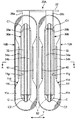
図3に示すように、各電極体10は、帯状の負極体11、帯状の正極体12、及び2枚の帯状のセパレータ13が互いに積層されながら巻回された巻回体である。より具体的に、負極体11、正極体12及びセパレータ13は、長円状の端面11e,12eを形成するように面状の巻回中心C周りに巻回され、これにより、扁平な巻回型の電極体10が形成されている。端面11e,12e側から見て、巻回中心Cは細長い長円状である。ケース2内において、各電極体10は、巻回中心Cが略上下方向に沿うような姿勢で配置され、2つの電極体10A,10Bは厚み方向(矢印Y方向)に並べて配置される(図4及び図5参照)。
As shown in FIG. 3, each
セパレータ13は、負極体11と正極体12の間に介装されることで、両者を電気的に絶縁している。セパレータ13は、例えば、多孔性の樹脂フィルムで構成されている。
The
負極体11は、負極金属箔11aと、負極金属箔11aに負極活物質を塗工して設けた負極活物質層11bと、を備えている。負極活物質層11bは、セパレータ13により全体が覆われる。負極体11の巻回軸方向(図3における符号Xで示す方向)一端部には、活物質が塗工されていない負極未塗工部11cが設けられている。負極未塗工部11cは、正極体12及びセパレータ13よりも巻回軸方向外側にはみ出して配置され、負極リード部11dを構成している。具体的に、負極リード部11dは、負極未塗工部11cのみが複数層に積層されながら巻回された扁平な巻回体で構成されている。
The
負極金属箔11aの材料には、例えば銅が用いられるが、これ以外の金属を用いてもよい。負極活物質としては、例えばグラファイト層間化合物が用いられるが、他の炭素材料、リチウム金属、リチウム合金、チタン酸リチウム(Li4Ti5O12)、ケイ素、一酸化ケイ素、スズ等のリチウム吸蔵可能な材料、またはこれらの混合物を用いてもよい。
For example, copper is used as the material of the negative
正極体12は、正極金属箔12aと、正極金属箔12aに正極活物質を塗工して設けた正極活物質層12bと、を備えている。正極活物質層12bは、セパレータ13により全体が覆われる。正極体12の巻回軸方向一端部には、活物質が塗工されていない正極未塗工部12cが設けられている。正極未塗工部12cは、巻回軸方向において負極未塗工部11cとは反対側に設けられている。正極未塗工部12cは、負極体11及びセパレータ13よりも巻回軸方向外側にはみ出して配置され、正極リード部12dを構成している。具体的に、正極リード部12dは、正極未塗工部12cのみが複数層に積層されながら巻回された扁平な巻回体で構成されている。
The
正極金属箔12aの材料には、例えばアルミニウムが用いられるが、これ以外の金属を用いてもよい。正極活物質としては、例えば、マンガン酸リチウム(LiMn2O4)、ニッケルコバルトマンガン酸リチウム(LiNixCoyMn1−x−yO2)、コバルト酸リチウム(LiCoO2)、ニッケル酸リチウム(LiNiO2)、リン酸鉄リチウム(LiFePO4)、リン酸マンガンリチウム(LiMnPO4)、これらに置換添加物を用いたもの、又は、これらの混合物などが用いられるが、他のリチウム含有遷移金属酸化物を用いてもよい。
For example, aluminum is used as the material of the positive
以上のように構成された電極体10は、巻回軸方向の両端部にリード部11d,12dを有し、負極リード部11dと正極リード部12dとの間に本体部10aを有する。負極リード部11d、正極リード部12d及び本体部10aは、共通の巻回中心C及び共通の巻回軸方向を有する扁平な巻回体で構成されている。以下、電極体10全体の「巻回中心C」又は「巻回軸方向」に言及する場合、及び、負極リード部11d、正極リード部12d又は本体部10aのいずれか1つの「巻回中心C」又は「巻回軸方向」に言及する場合のいずれにおいても、単に「巻回中心C」又は「巻回軸方向」ということがある。
The
以下、集電体20(20A,20B)及びこれに関連する構成について実施形態毎に説明する。 Hereinafter, the current collector 20 (20A, 20B) and the configuration related thereto will be described for each embodiment.
[第1の実施形態]
図4〜図6に示すように、負極集電体20Aは、2つの電極体10A,10Bの各負極リード部11dに接合され、これらの負極リード部11dを負極外部端子14に電気的に接続する。負極集電体20Aの材料には、例えば、銅等の金属が用いられる。同様に、正極集電体20Bは、2つの電極体10A,10Bの各正極リード部12dに接合され、これらの正極リード部12dを正極外部端子15に電気的に接続する。正極集電体20Bの材料には、例えば、アルミニウム等の金属が用いられる。なお、図5及び図6は、集電体20と電極体10との接合構造を説明するために負極側の構造のみを代表的に図示しているが、正極側の構造も負極側の構造と同様である。
[First Embodiment]
As shown in FIGS. 4 to 6, the negative electrode
負極集電体20Aと正極集電体20Bとは互いに同じ形状を有する。以下、集電体20(20A,20B)の形状及びこれに関連する構成について説明する。
The negative electrode
図7及び図8に示すように、第1の実施形態に係る集電体20は、蓋体4の下面に固定される基部22と、それぞれ第1延長部26a,26b及び第2延長部28a,28bを介して基部22の下方に連なる第1集電部30a及び第2集電部30bとを備えている。
As shown in FIGS. 7 and 8, the
負極集電体20Aの基部22は、蓋体4の下面に下パッキン18を介して固定され、負極外部端子14に電気的に接続される。正極集電体20Bの基部22は、蓋体4の下面に下パッキン18を介して固定され、正極外部端子15に電気的に接続される(図2参照)。蓋体4への基部22の固定には、例えば、基部22の貫通穴24に挿通されるリベットが用いられる。
The
図5、図7及び図8に示すように、第1延長部26a,26bは、電極体10の厚み方向(矢印Y方向)に互いに間隔を空けて一対設けられている。各第1延長部26a,26bは、基部22の巻回軸方向外側端部から下方に帯状に延設されている。集電体20と電極体10A,10Bとの接合状態において、第1延長部26a,26bは、リード部11d(12d)の端面11e(12e)に沿って、リード部11d(12d)の巻回中心Cの上端湾曲部C1よりも下側に突出しないように配置される。すなわち、リード部11d(12d)の端面側から見て、第1延長部26a,26bは、巻回中心Cに対して、上端湾曲部C1のみに重なり、上端湾曲部C1よりも下側の部分には重ならないように配置される。第2延長部28a,28bは、各第1延長部26a,26bの下端から巻回軸方向内側へ帯状に延設されており、リード部11d(12d)の巻回中心Cの上端部に挿入される。
As shown in FIGS. 5, 7, and 8, a pair of first extending
図5及び図6に示すように、第1集電部30aと第2集電部30bとは、2つの電極体10A,10Bの並び方向(各電極体10A,10Bの厚み方向、すなわち、矢印Y方向)に互いに間隔を空けて配置されている。第1集電部30aは、一方の電極体10B(10A)のリード部11d(12d)に接合され、第2集電部30bは、他方の電極体10A(10B)のリード部11d(12d)に接合される。具体的に、負極集電体20Aの第1集電部30aは第2電極体10Bの負極リード部11dに接合され、負極集電体20Aの第2集電部30bは第1電極体10Aの負極リード部11dに接合される。他方、正極集電体20Bの第1集電部30aは第2電極体10Bの正極リード部12dに接合され、正極集電体20Bの第2集電部30bは第1電極体10Aの正極リード部12dに接合される。
As shown in FIG.5 and FIG.6, the 1st
図5〜図8に示すように、各集電部30a,30bは、対応する電極体10A,10Bのリード部11d(12d)の巻回中心Cに挿入されて、リード部11d(12d)の内周11g(12g)に接合される。
As shown in FIGS. 5 to 8, each of the
各集電部30a,30bは、リード部11d(12d)の巻回中心Cの内部空間を巻回軸方向に仕切るように配置される隔壁部32と、該隔壁部32から巻回軸方向外側に突設されてリード部11d(12d)の内周11g(12g)に接合される一対の被接合壁部34a,34bと、を有する。
Each of the
隔壁部32は、第2延長部28a,28bの先端から下方へ帯状に延設されている。隔壁部32は、リード部11d(12d)の巻回中心Cにおいて、巻回軸方向に略直角な面に沿って且つリード部11d(12d)の端面11e(12e)側から見て巻回中心Cの長さ方向に沿って配置される。また、リード部11d(12d)の端面11e(12e)側から見て、隔壁部32は、リード部11d(12d)の巻回中心Cにおける上端湾曲部C1および下端湾曲部C2を除く部分の全長に亘って延びるように配置される。
The
なお、図5及び図6に図示された例では、電極体10A,10Bの厚み方向(矢印Y方向)に関して、巻回中心Cの幅は、本体部10aにおいては隔壁部32よりも小さな幅となっているが、リード部11d(12d)においては、内周側に配置された集電部30a,30bによって外側へ押し拡げられることにより、隔壁部32の幅以上の幅となっている。また、図5及び図6に図示された例では、集電部30a,30bを挟んだ両側において、リード部11d(12d)を構成する複数の箔は、厚み方向(矢印Y方向)の中央部に集められて集電部30a,30bに溶接されている。ただし、集電部30a,30bの幅が図示された例よりも小さい場合、リード部11d(12d)を構成する複数の箔は、図示された位置よりも内周側に集められて集電部30a,30bに溶接される。逆に、集電部30a,30bの幅が図示された例よりも大きい場合、リード部11d(12d)を構成する複数の箔は、図示された位置よりも外周側に集められて集電部30a,30bに溶接される。
In the example illustrated in FIGS. 5 and 6, the width of the winding center C in the thickness direction (arrow Y direction) of the
一対の被接合壁部34a,34bは、巻回中心Cを挟んだ一方の側(図5及び図6における左側)においてリード部11d(12d)の内周11g(12g)に接合される第1被接合壁部34aと、第1被接合壁部34aからリード部11d(12d)の厚み方向(矢印Y方向)に間隔を空けて配置され、巻回中心Cを挟んだ他方の側(図5及び図6における右側)においてリード部11d(12d)の内周11g(12g)に接合される第2被接合壁部34bとで構成されている。
The pair of joined
第1被接合壁部34aは、隔壁部32の短手方向一端部から巻回軸方向外側に突出しており、第2被接合壁部34bは、隔壁部32の短手方向他端部から巻回軸方向外側に突出している。第1被接合壁部34aと第2被接合壁部34bとは、それぞれ、隔壁部32に略直角な面に沿って、上下方向に帯状に延びるように設けられている。これにより、平面から見た集電部30a,30bの断面形状は、巻回軸方向外側に開放するU字形となっている(図6参照)。集電部30a,30bは、開放部とは反対側、すなわち隔壁部32側からリード部11d(12d)の巻回中心Cに挿入されるため、挿入時に被接合壁部34a,34bがリード部11d(12d)の箔に引っ掛かり難く、箔の損傷が抑制される。
The first bonded
また、第1被接合壁部34aと第2被接合壁部34bとは、隔壁部32の略全長に亘って設けられている。第1被接合壁部34a及び第2被接合壁部34bの巻回軸方向外側の上端コーナー部36及び下端コーナー部38は面取り加工されている。
The first bonded
図5及び図6に示すように、第1被接合壁部34aと第2被接合壁部34bとは、リード部11d(12d)の内周11g(12g)における上下方向に延びる部分に沿って配置され、例えば超音波溶接によってリード部11d(12d)に接合される。なお、図5及び図6に示す例では、被接合壁部34a,34bと金属製の押さえプレート40との間にリード部11d(12d)を挟み込んだ状態で超音波溶接が行われる。第1集電部30aと第2集電部30bは、被接合壁部34a,34bがリード部11d(12d)の内周11g(12g)に接合されることで、電極体10A,10Bに電気的に接続される。このような接合構造により、2つの電極体10A,10Bは、各負極リード部11dに接合された負極集電体20Aと、各正極リード部12dに接合された正極集電体20Bとによって吊り下げ支持される。
As shown in FIG.5 and FIG.6, the 1st to-
第1の実施形態によれば、各集電部30a,30bは、巻回中心Cを挟んだ両側においてリード部11d(12d)の内周11g(12g)に接合されるため、リード部11d(12d)に対する集電部30a,30bの取付け状態を安定させることができる。さらに、各集電部30a,30bにおいて、一対の被接合壁部34a,34bは隔壁部32を介して断面U字状に連なっているため、集電部30a,30bの剛性が高められている。
According to the first embodiment, the
また、第1の実施形態によれば、被接合壁部34a,34bよりも巻回軸方向内側において、隔壁部32がリード部11d(12d)の巻回中心Cの略全長に亘って延びるように配置されるため、例えば超音波溶接によってリード部11d(12d)と被接合壁部34a,34bとを接合するときに飛散する金属粉末は、巻回軸方向内側への移動が隔壁部32によって規制される。また、集電部30a,30bは、巻回中心Cにおける上端湾曲部C1および下端湾曲部C2を除いた略全周に亘ってリード部11d(12d)の内周11g(12g)に接合される。この接合部分において、隔壁部32とリード部11d(12d)の内周11g(12g)との間に隙間が生じないため、隔壁部32とリード部11d(12d)の内周11g(12g)との間を通って電極体10A,10Bの内部に金属粉末が入り込むことを効果的に抑制できる。特に、負極リード部11dの巻回中心Cから銅粉末が入り込むことを抑制することで、銅粉末が負極側から正極側へ移動したときに生じ得る蓄電素子1の微小短絡による容量低下を抑制できる。
Further, according to the first embodiment, the
第1の実施形態に係る集電体20は、1枚の金属板を所定形状に切り抜いて折り曲げることによって簡単に成形することができる。具体的には、図7及び図8に示すように、一対の第1延長部26a,26bをそれぞれ折り目R1に沿って基部22に対して略直角に折り曲げ、一対の第2延長部28a,28bをそれぞれ折り目R2に沿って第1延長部26a,26bに対して略直角に折り曲げ、一対の集電部30a,30bの各隔壁部32をそれぞれ折り目R3に沿って第2延長部28a,28bに対して略直角に折り曲げる。また、集電部30a,30b毎に、一対の被接合壁部34a,34bをそれぞれ折り目R4,R5に沿って隔壁部32に対して略直角に折り曲げる。このように、ねじりを加えるような高度な加工を行うことなく、金属板を直角に複数回折り曲げるだけで簡単に集電体20を成形することができる。
The
ところで、リード部11d(12d)の外周を一対の脚部で挟み込むタイプの集電体を用いる場合には、リード部11d(12d)の上端湾曲部を集電体の脚部の付け根部分に干渉しないように変形させるフォーミング加工が行われることがある。これに対して、本実施形態に係る集電体20を用いる場合、電極体10A,10Bに上記のようなフォーミング加工を施す必要がないため、蓄電素子1の生産性が高められる。
By the way, when a current collector of a type in which the outer periphery of the
[第2の実施形態]
図9及び図10を参照しながら、第2の実施形態に係る集電体50の構成について説明する。なお、第1の実施形態と同じ構成要素については、説明を省略するとともに、図9及び図10において同じ符号を付している。
[Second Embodiment]
The configuration of the
図9及び図10に示すように、第2の実施形態では、各集電部30a,30bに、隔壁部32の下端部から巻回軸方向外側に突出する突出壁部52が設けられている。突出壁部52は、隔壁部32に略直角な面に沿って配置された矩形の板状部で構成されている。突出壁部52は、折り目R6に沿って隔壁部32に対して略直角に折り曲げることで形成される。そのため、第2の実施形態に係る集電体50は、第1の実施形態と同様、1枚の金属板を切り抜いて折り曲げることで容易に成形することができる。
As shown in FIGS. 9 and 10, in the second embodiment, the
図5及び図6の二点鎖線に示されるように、第2の実施形態によれば、突出壁部52は、隔壁部32よりも巻回軸方向外側において、例えば電極体10A,10Bのリード部11d,12dと被接合壁部34a,34bとの溶接時に発生する金属粉末の下方への移動を遮断するように配置される。そのため、金属粉末が隔壁部32の下端とリード部11d,12dの内周11g,12gとの間を通って電極体10A,10Bの内部に入り込むことを抑制できる。
As shown by the two-dot chain line in FIGS. 5 and 6, according to the second embodiment, the protruding
なお、隔壁部32の上端部には、第2延長部28a,28bが巻回軸方向外側に突設されているため、隔壁部32よりも巻回軸方向外側における金属粉末の上方への移動は第2延長部28a,28bによって遮断される。そのため、隔壁部32の上端とリード部11d,12dの内周11g,12gとの間を経由した金属粉末の侵入も効果的に抑制される。
In addition, since the
[第3の実施形態]
図11を参照しながら、第3の実施形態に係る集電体60の構成について説明する。なお、第1の実施形態と同じ構成要素については、説明を省略するとともに、図11において同じ符号を付している。
[Third Embodiment]
The configuration of the
図11に示すように、第3の実施形態に係る集電体60は、集電部30を1つのみ有する点で、第1の実施形態に係る集電体20と異なる。そのため、集電体60には1つの電極体10のみが接合される。したがって、第3の実施形態に係る集電体60は、蓄電素子1が電極体10を1つのみ有する場合に好適に用いられる。なお、集電体60の別の用途として、集電体60の集電部30を挟んだ両側に電極体を配置して、これら2つの電極体を集電部30に接合することも可能である。この場合、一方の電極体のリード部の外周を第1被接合壁部34aに接合し、他方の電極体のリード部の外周を第2被接合壁部34bに接合すればよい。
As shown in FIG. 11, the
第3の実施形態においても、第1の実施形態と同様、集電部30は、第1延長部26及び第2延長部28を介して基部22の下方に連ねて設けられ、該集電部30には、隔壁部32と一対の被接合壁部34a,34bとが設けられている。そのため、第1の実施形態と同様、集電部30は、電極体10の内部への金属粉末の侵入を規制しつつ、該電極体10のリード部11d,12dの内周11g,12gに接合される。
Also in the third embodiment, as in the first embodiment, the
また、第2の実施形態と同様、集電部30には、隔壁部32の下端部から巻回軸方向外側に突出する突出壁部62が設けられている。そのため、第2の実施形態と同様、金属粉末が隔壁部32の下端とリード部11d,12dの内周11g,12gとの間を通って電極体10A,10Bの内部に入り込むことを抑制できる。ただし、第3の実施形態において、突出壁部62を省略してもよい。
Similarly to the second embodiment, the
[第4の実施形態]
図12を参照しながら、第4の実施形態に係る集電体70の構成について説明する。なお、第1の実施形態と同じ構成要素については、説明を省略するとともに、図12において同じ符号を付している。
[Fourth Embodiment]
The configuration of the
図12に示すように、第4の実施形態に係る集電体70が有する集電部30a,30bは、隔壁部32と該隔壁部32の周縁部から立ち上がる周壁72とを備えた筐体で構成されている。隔壁部32の形状は長尺の矩形であり、周壁72の形状は、隔壁部32の輪郭と同じ断面形状を有する角筒状である。これにより、周壁72には、互いに対向する一対の長尺壁部34a,34bと、互いに対向する一対の短尺壁部74,76とが形成されている。一方の長尺壁部34aは第1被接合壁部を構成し、他方の長尺壁部34bは第2被接合壁部を構成する。
As shown in FIG. 12, the
このようにして構成された集電部30a,30bは、第1延長部26a,26bを介して基部22の下方に連なっている。第1の実施形態と同様、第1延長部26a,26bは、基部22の巻回軸方向外側端部から下方に帯状に延設されており、第1延長部26a,26bの下端に、集電部30a,30bにおける一方の短尺壁部74の巻回軸方向外側端部が連なっている。
The
第4の実施形態においても、集電部30a,30bは、電極体10A,10Bのリード部11d,12dの巻回中心Cに挿入されて、リード部11d,12dに接合される。具体的に、集電部30a,30bの隔壁部32は、リード部11d,12dの巻回中心Cの内部空間を巻回軸方向に仕切るように且つリード部11d,12dの端面11e,12e側から見て巻回中心Cの略全長に亘って延びるように配置され、集電部30a,30bの周壁72は、隔壁部32を挟んだ巻回軸方向外側に配置される。このように集電部30a,30bが配置された状態で、被接合壁部34a,34bは、第1の実施形態と同様、例えば超音波溶接によりリード部11d,12dの内周11g,12gに接合される。
Also in the fourth embodiment, the
このような接合構造によれば、被接合壁部34a,34bとリード部11d,12dとの接合により発生する金属粉末は、隔壁部32によって巻回軸方向内側への移動が遮断されるとともに、周壁72によって径方向外側から完全に包囲されるため、電極体10A,10Bの内部への金属粉末の侵入を効果的に抑制することができる。また、集電部30a,30bが筐体で構成されているため、集電部30a,30bの剛性を効果的に高めることができる。
According to such a joining structure, the metal powder generated by joining the to-
集電部30a,30bを構成する筐体は、成形型を用いたプレス加工によって極めて簡単に成形することができる。一方、基部22及び一対の第1延長部26a,26bは、1枚の金属板を所定形状に切り抜いて、各第1延長部26a,26bを折り目R1に沿って基部22に対して略直角に折り曲げることで成形される。このように成形された曲げ加工部分80に、上記のように成形型を用いて成形された集電部30a,30bが接合されることで、集電体70が形成される。曲げ加工部分80と集電部30a,30bとの接合は、曲げ加工部分80における各第1延長部26a,26bの先端に集電部30a,30bにおける短尺壁部74の縁部を例えば溶接により接合することで行われる。
The housing constituting the
第4の実施形態によれば、成形型を用いて集電部30a,30bを極めて簡単に成形することができるため、集電体70の生産性を高めることができる。よって、当該集電体70を備えた蓄電素子1の生産性を高めることができる。
According to the fourth embodiment, the
なお、第4の実施形態では、集電体70が一対の集電部30a,30bを有する場合について説明したが、蓄電素子1が電極体10を1つのみ有する場合、集電体70には、上記のように構成された集電部30a,30bを1つのみ設けるようにすればよい。
In the fourth embodiment, the case where the
以上、上述の実施形態を挙げて本発明を説明したが、本発明は上述の実施形態に限定されるものではない。 While the present invention has been described with reference to the above-described embodiments, the present invention is not limited to the above-described embodiments.
例えば、上述の実施形態では、蓄電素子が1つ又は2つの電極体を有する場合について説明したが、本発明は、蓄電素子が3つ以上の電極体を有する場合にも適用できる。この場合、集電体には、電極体の個数と同数の集電部を設ければよい。 For example, in the above-described embodiment, the case where the power storage element has one or two electrode bodies has been described. However, the present invention can also be applied to a case where the power storage element has three or more electrode bodies. In this case, the current collector may be provided with the same number of current collectors as the number of electrode bodies.
また、上述の実施形態では、超音波溶接によって集電体と電極体のリード部とが接合される場合について説明したが、本発明において、集電体と電極体のリード部との接合は、例えば、抵抗溶接、レーザ溶接、機械的接合方法によって行ってもよい。 In the above-described embodiment, the case where the current collector and the lead portion of the electrode body are joined by ultrasonic welding has been described, but in the present invention, the joining of the current collector and the lead portion of the electrode body is performed as follows. For example, resistance welding, laser welding, or a mechanical joining method may be used.
1 :蓄電素子
2 :ケース
3 :ケース本体
4 :蓋体
8 :安全弁
9 :液栓
10 :電極体
10a :本体部
11 :負極体
11a :負極金属箔
11b :負極活物質層
11c :負極未塗工部
11d :負極リード部
11e :負極側の端面
11f :負極リード部の外周
11g :負極リード部の内周
12 :正極体
12a :正極金属箔
12b :正極活物質層
12c :正極未塗工部
12d :正極リード部
12e :正極側の端面
12f :正極リード部の外周
12g :正極リード部の内周
13 :セパレータ
14 :負極外部端子
15 :正極外部端子
16 :上パッキン
18 :下パッキン
20A :負極集電体
20B :正極集電体
22 :基部
30a :第1集電部
30b :第2集電部
32 :隔壁部
34a :第1被接合壁部
34b :第2被接合壁部
40 :押さえプレート
50 :集電体
52 :突出壁部
60 :集電体
62 :突出壁部
70 :集電体
72 :周壁
74,76:短尺壁部
80 :曲げ加工部分
C :巻回中心
X :巻回軸
Y :電極体(リード部)の厚み方向
DESCRIPTION OF SYMBOLS 1: Power storage element 2: Case 3: Case main body 4: Cover body 8: Safety valve 9: Liquid stopper 10: Electrode body 10a: Main body part 11: Negative electrode body 11a: Negative electrode metal foil 11b: Negative electrode active material layer 11c: Negative electrode uncoated Work part 11d: Negative electrode lead part 11e: Negative electrode side end face 11f: Negative electrode lead part outer periphery 11g: Negative electrode lead part inner circumference 12: Positive electrode body 12a: Positive electrode metal foil 12b: Positive electrode active material layer 12c: Positive electrode uncoated part 12d: Positive electrode lead part 12e: Positive electrode side end face 12f: Positive electrode lead part outer periphery 12g: Positive electrode lead part inner periphery 13: Separator 14: Negative electrode external terminal 15: Positive electrode external terminal 16: Upper packing 18: Lower packing 20A: Negative electrode Current collector 20B: Positive electrode current collector 22: Base 30a: First current collector 30b: Second current collector 32: Partition wall 34a: First bonded wall 34b : Second bonded wall 40: Holding plate 50: Current collector 52: Protruding wall portion 60: Current collector 62: Protruding wall portion 70: Current collector 72: Peripheral wall 74, 76: Short wall portion 80: Bending Part C: Winding center X: Winding axis Y: Thickness direction of electrode body (lead part)
Claims (5)
前記リード部を外部端子に電気的に接続する集電体と、を備え、
前記集電体は、
前記リード部の巻回中心の内部空間を巻回軸方向に仕切るように且つ前記リード部の端面側から見て前記巻回中心の略全長に亘って延びるように配置された隔壁部と、
該隔壁部から巻回軸方向外側に突設されて前記リード部の内周に接合される被接合壁部と、
前記隔壁部の長さ方向先端部から巻回軸方向外側に突出する突出壁部と、を備えることを特徴とする蓄電素子。 An electrode body having a lead portion composed of a flat wound body around which a metal foil is wound;
A current collector that electrically connects the lead portion to an external terminal;
The current collector is
A partition part disposed so as to partition the inner space of the winding center of the lead part in the winding axis direction and to extend over substantially the entire length of the winding center as seen from the end face side of the lead part;
A to-be-joined wall portion protruding from the partition wall to the outside in the winding axis direction and joined to the inner periphery of the lead portion;
And a protruding wall portion protruding outward in the winding axis direction from the longitudinal end portion of the partition wall portion .
前記リード部を外部端子に電気的に接続する集電体と、を備え、
前記集電体は、それぞれ異なる1つの電極体のリード部に接合される複数の集電部を備え、
各集電部は、
前記リード部の巻回中心の内部空間を巻回軸方向に仕切るように且つ前記リード部の端面側から見て前記巻回中心の略全長に亘って延びるように配置された隔壁部と、
該隔壁部から巻回軸方向外側に突設されて前記リード部の内周に接合される被接合壁部と、を備えることを特徴とする蓄電素子。 A plurality of electrode bodies having a lead portion made of a flat wound body around which a metal foil is wound;
A current collector that electrically connects the lead portion to an external terminal;
The current collector includes a plurality of current collectors joined to lead portions of different one electrode bodies,
Each current collector is
A partition part disposed so as to partition the inner space of the winding center of the lead part in the winding axis direction and to extend over substantially the entire length of the winding center as seen from the end face side of the lead part;
And a to-be-joined wall portion that protrudes outward from the partition wall in the winding axis direction and is joined to the inner periphery of the lead portion.
前記巻回中心を挟んだ一方の側において前記リード部の内周に接合される第1被接合壁部と、
第1被接合壁部から前記リード部の厚み方向に間隔を空けて配置され、前記巻回中心を挟んだ他方の側において前記リード部の内周に接合される第2被接合壁部と、を含むことを特徴とする請求項1または請求項2に記載の蓄電素子。 The wall to be joined is
A first wall portion to be bonded to the inner periphery of the lead portion on one side across the winding center;
A second to-be-joined wall portion that is arranged at an interval from the first to-be-joined wall portion in the thickness direction of the lead portion and is joined to the inner periphery of the lead portion on the other side across the winding center; The electricity storage device according to claim 1 , comprising:
隔壁部と該隔壁部の周縁部から立ち上がる周壁とを備えた筐体をプレス加工によって成形して、該筐体を有する前記集電体を形成し、
前記隔壁部を挟んだ巻回軸方向外側において、前記周壁に前記リード部の内周を接合する、ことを特徴とする蓄電素子の製造方法。 A method for manufacturing a power storage device, which manufactures a power storage device comprising: an electrode body having a lead portion made of a wound body in which a metal foil is wound; and a current collector that electrically connects the lead portion to an external terminal. Because
A casing having a partition wall and a peripheral wall rising from the peripheral edge of the partition wall is molded by pressing to form the current collector having the casing,
A method for manufacturing a storage element, comprising: joining an inner periphery of the lead portion to the peripheral wall on an outer side in a winding axis direction with the partition wall interposed therebetween.
Priority Applications (1)
| Application Number | Priority Date | Filing Date | Title |
|---|---|---|---|
| JP2013189084A JP6155997B2 (en) | 2013-09-12 | 2013-09-12 | Power storage device and method for manufacturing power storage device |
Applications Claiming Priority (1)
| Application Number | Priority Date | Filing Date | Title |
|---|---|---|---|
| JP2013189084A JP6155997B2 (en) | 2013-09-12 | 2013-09-12 | Power storage device and method for manufacturing power storage device |
Publications (2)
| Publication Number | Publication Date |
|---|---|
| JP2015056288A JP2015056288A (en) | 2015-03-23 |
| JP6155997B2 true JP6155997B2 (en) | 2017-07-05 |
Family
ID=52820559
Family Applications (1)
| Application Number | Title | Priority Date | Filing Date |
|---|---|---|---|
| JP2013189084A Expired - Fee Related JP6155997B2 (en) | 2013-09-12 | 2013-09-12 | Power storage device and method for manufacturing power storage device |
Country Status (1)
| Country | Link |
|---|---|
| JP (1) | JP6155997B2 (en) |
Families Citing this family (4)
| Publication number | Priority date | Publication date | Assignee | Title |
|---|---|---|---|---|
| JP7024286B2 (en) * | 2017-09-27 | 2022-02-24 | 株式会社Gsユアサ | Power storage element |
| JP7024288B2 (en) * | 2017-09-27 | 2022-02-24 | 株式会社Gsユアサ | Power storage element |
| JP6950406B2 (en) * | 2017-09-27 | 2021-10-13 | 株式会社Gsユアサ | Power storage element |
| JP2019061893A (en) * | 2017-09-27 | 2019-04-18 | 株式会社Gsユアサ | Power storage element |
Family Cites Families (2)
| Publication number | Priority date | Publication date | Assignee | Title |
|---|---|---|---|---|
| JP4374870B2 (en) * | 2003-03-06 | 2009-12-02 | トヨタ自動車株式会社 | Power storage device in which terminal and electrode foil are plastically bonded, and manufacturing method thereof |
| JP4661257B2 (en) * | 2005-02-17 | 2011-03-30 | トヨタ自動車株式会社 | Current collecting terminal and power storage device including the terminal |
-
2013
- 2013-09-12 JP JP2013189084A patent/JP6155997B2/en not_active Expired - Fee Related
Also Published As
| Publication number | Publication date |
|---|---|
| JP2015056288A (en) | 2015-03-23 |
Similar Documents
| Publication | Publication Date | Title |
|---|---|---|
| JP7367742B2 (en) | Energy storage element | |
| US10388939B2 (en) | Secondary battery | |
| JP6293501B2 (en) | Secondary battery and method for manufacturing secondary battery | |
| JP5841571B2 (en) | Secondary battery | |
| WO2013111256A1 (en) | Secondary battery | |
| JP5742869B2 (en) | Power storage device | |
| WO2015098955A1 (en) | Electricity storage device | |
| US20110076544A1 (en) | Stack type battery | |
| JP6155997B2 (en) | Power storage device and method for manufacturing power storage device | |
| KR20140035249A (en) | Electric storage device | |
| JP5677373B2 (en) | battery | |
| US10516152B2 (en) | Energy storage device | |
| JP6701210B2 (en) | Electric storage element and method for manufacturing electric storage element | |
| US10734655B2 (en) | Electric storage device | |
| WO2017098690A1 (en) | Cell | |
| JP6715936B2 (en) | Prismatic secondary battery | |
| JP6307813B2 (en) | Electricity storage element | |
| JP2015069800A (en) | Storage element and manufacturing method of storage element | |
| JP7318333B2 (en) | Storage element | |
| JP6375610B2 (en) | Storage element and method for manufacturing the same | |
| WO2015186834A1 (en) | Secondary battery | |
| JP6045799B2 (en) | Flat battery | |
| JP2015008085A (en) | Power storage element | |
| JP7322872B2 (en) | Storage element | |
| JP2018116867A (en) | Power storage element, and manufacturing method of power storage element |
Legal Events
| Date | Code | Title | Description |
|---|---|---|---|
| A621 | Written request for application examination |
Free format text: JAPANESE INTERMEDIATE CODE: A621 Effective date: 20160412 |
|
| A977 | Report on retrieval |
Free format text: JAPANESE INTERMEDIATE CODE: A971007 Effective date: 20170215 |
|
| A131 | Notification of reasons for refusal |
Free format text: JAPANESE INTERMEDIATE CODE: A131 Effective date: 20170221 |
|
| A521 | Request for written amendment filed |
Free format text: JAPANESE INTERMEDIATE CODE: A523 Effective date: 20170418 |
|
| TRDD | Decision of grant or rejection written | ||
| A01 | Written decision to grant a patent or to grant a registration (utility model) |
Free format text: JAPANESE INTERMEDIATE CODE: A01 Effective date: 20170509 |
|
| A61 | First payment of annual fees (during grant procedure) |
Free format text: JAPANESE INTERMEDIATE CODE: A61 Effective date: 20170522 |
|
| R150 | Certificate of patent or registration of utility model |
Ref document number: 6155997 Country of ref document: JP Free format text: JAPANESE INTERMEDIATE CODE: R150 |
|
| LAPS | Cancellation because of no payment of annual fees |