JP6151970B2 - Touch panel with pressure measurement - Google Patents
Touch panel with pressure measurement Download PDFInfo
- Publication number
- JP6151970B2 JP6151970B2 JP2013110655A JP2013110655A JP6151970B2 JP 6151970 B2 JP6151970 B2 JP 6151970B2 JP 2013110655 A JP2013110655 A JP 2013110655A JP 2013110655 A JP2013110655 A JP 2013110655A JP 6151970 B2 JP6151970 B2 JP 6151970B2
- Authority
- JP
- Japan
- Prior art keywords
- electrode
- touch panel
- conductor
- piezoelectric body
- electrodes
- Prior art date
- Legal status (The legal status is an assumption and is not a legal conclusion. Google has not performed a legal analysis and makes no representation as to the accuracy of the status listed.)
- Expired - Fee Related
Links
Images


Description
本発明は、圧電体を使用する力測定と静電容量方式の位置検出を備えたタッチパネルに関する。 The present invention relates to a touch panel including force measurement using a piezoelectric body and electrostatic capacitance type position detection.
タッチパネルにあって静電センサは入力位置を検出する。圧電センサは押圧力を測定する。 The electrostatic sensor in the touch panel detects the input position. The piezoelectric sensor measures the pressing force.
従来、静電センサと圧電センサを兼備し、位置検出と力測定を行うタッチパネルが知られている(例えば特許文献1、特許文献2参照)。これら従来のタッチパネルは圧電センサの上面又は下面に静電センサが重ねられている。2種のセンサを単に重ね合わせただけでは、タッチパネルが厚くなり、透明性などの光学特性が変わり、製造コストも上がる。
Conventionally, a touch panel that combines an electrostatic sensor and a piezoelectric sensor and performs position detection and force measurement is known (see, for example,
本発明が解決しようとする問題点は、静電センサと圧電センサを兼備するタッチパネルにおいて不都合となる、パネルが厚くなる点、光学特性が変わる点と製造コストが上がる点である。 The problems to be solved by the present invention are inconvenience in a touch panel having both an electrostatic sensor and a piezoelectric sensor, in that the panel becomes thick, the optical characteristics change, and the manufacturing cost increases.
本発明のその他の課題は、本発明の説明により明らかになる。 Other problems of the present invention will become apparent from the description of the present invention.
以下に課題を解決するための手段を述べる。理解を容易にするために、本発明の実施態様に対応する符号を付けて説明するが、本発明は当該実施態様に限定されるものではない。また、符号である数字は部品などを集合的に示す場合があり、後に説明する実施例において個別の部品などを示す場合に、当該数字のあとにアルファベットの添字を付けているものがある。 Means for solving the problems will be described below. For ease of understanding, description will be made with reference numerals corresponding to the embodiments of the present invention, but the present invention is not limited to the embodiments. A number as a symbol may indicate a part or the like collectively. When an individual part or the like is indicated in an embodiment described later, an alphabetic suffix may be added after the number.
本発明の一の態様にかかるタッチパネルは、
圧電体を使用し力を検出する力検出と位置を検出する位置検出とを備えた投影型静電容量方式タッチパネル(40)であって
前記タッチパネルは圧電体(31)と前記圧電体上に配置されるTP専用電極(18)からなり、
力検出は電極を使用して前記圧電体に力が負荷されたときに前記圧電体に生じる電力を測定するものであり、
位置検出は一組の電極を使用するものであり、前記一組の電極のうち一の電極はXY平面上の一の方向に平行に配置された一群の導電体からなり、他の電極は前記一の方向と交差する方向に平行に配置された一群の他の導電体からなり、
前記TP専用電極は、力検出に使用する電極、位置検出に使用する電極及び力検出と位置検出を兼用する電極である。
The touch panel according to one aspect of the present invention includes:
A projected capacitive touch panel (40) having force detection for detecting force using a piezoelectric body and position detection for detecting a position, wherein the touch panel is disposed on the piezoelectric body (31) and the piezoelectric body. TP dedicated electrode (18)
Force detection is to measure the electric power generated in the piezoelectric body when a force is applied to the piezoelectric body using an electrode,
The position detection uses a set of electrodes, and one electrode of the set of electrodes is composed of a group of conductors arranged in parallel in one direction on the XY plane, and the other electrodes are the above-described electrodes. Consisting of a group of other conductors arranged parallel to a direction intersecting one direction,
The TP-dedicated electrode is an electrode used for force detection, an electrode used for position detection, and an electrode that combines force detection and position detection.
本発明にかかるタッチパネルにあって、TP専用電極は、
(1) 力測定のみに使用する電極、
(2) 位置検出のみに使用する電極、及び
(3) 力測定と位置検出を兼用しこれらのみに使用する電極
である。TP専用電極は圧電体の上面側に位置付けられている。
In the touch panel according to the present invention, the electrode for TP is
(1) electrodes used only for force measurement,
(2) electrodes used only for position detection, and
(3) This electrode is used only for force measurement and position detection. The TP dedicated electrode is positioned on the upper surface side of the piezoelectric body.
タッチパネルは、通常、表示装置に重ねて配置し、電子機器として使用される。また、タッチパネルは通常、平板、シート又はフィルム形状である。タッチパネルは表示装置の表示面を構成している表面部材の上に載置される。 The touch panel is usually placed on a display device and used as an electronic device. Moreover, a touch panel is a flat plate, a sheet | seat, or a film shape normally. A touch panel is mounted on the surface member which comprises the display surface of a display apparatus.
圧電体の下面は直接表面部材と接しているか、又は、圧電体の下面は電気絶縁性の部材を介在して表面部材と接している。 The lower surface of the piezoelectric body is in direct contact with the surface member, or the lower surface of the piezoelectric body is in contact with the surface member through an electrically insulating member.
本発明の第一のグループに属するタッチパネルにあって、その好ましい実施態様は、
前記圧電体が、力を受けるとXY平面に平行な面内で電荷が発生するXY平面分極性圧電体である。
In the touch panel belonging to the first group of the present invention, its preferred embodiment is:
The piezoelectric body is an XY plane polarizable piezoelectric body that generates electric charges in a plane parallel to the XY plane when receiving a force.
XY平面分極性圧電体であれば、力測定にかかる一対の電極を圧電体の同一平面側に配置することができる利点がある。 An XY plane polarizable piezoelectric body has an advantage that a pair of electrodes for force measurement can be arranged on the same plane side of the piezoelectric body.
本発明の好ましい実施態様にあって、
前記TP専用電極は、力検出のみに使用する一対の電極及び位置検出のみに使用する一組の電極からなるものであってもよく、また、前記TP専用電極は、力検出に使用する単一の電極と、位置検出に使用する一組の電極のうちの単一の電極と力検出に使用する電極と位置検出に使用する電極を兼用する単一の電極からなるものであってもよい。力検出に使用する電極と位置検出に使用する電極を兼用する単一の電極を使用すれば電極数を少なくできる利点がある。
In a preferred embodiment of the present invention,
The TP dedicated electrode may be composed of a pair of electrodes used only for force detection and a set of electrodes used only for position detection, and the TP dedicated electrode is a single electrode used for force detection. And a single electrode that serves as both a single electrode of a set of electrodes used for position detection, an electrode used for force detection, and an electrode used for position detection. There is an advantage that the number of electrodes can be reduced by using a single electrode that serves both as an electrode used for force detection and an electrode used for position detection.
本発明の好ましい他の実施態様にかかるタッチパネルは、
表示装置の表示面に載置して用いられるタッチパネルであって、前記表示装置は表示面から出射される可視光が直線偏光である。同時に、前記タッチパネルを構成する前記圧電体は位相差板であり、前記圧電体である位相差板の遅相軸が、前記直線偏光の振動面に対して20度から70度の角度で配置されて使用されてもよい。そして、前記圧電体のリタデーション値が、
(1)110nm以上170nm以下、または
(2)800nm以上30,000nm以下のいずれかであってもよい。
A touch panel according to another preferred embodiment of the present invention includes:
The touch panel is used by being placed on a display surface of a display device, wherein the visible light emitted from the display surface is linearly polarized light. At the same time, the piezoelectric body constituting the touch panel is a phase difference plate, and the slow axis of the phase difference plate which is the piezoelectric body is arranged at an angle of 20 degrees to 70 degrees with respect to the vibration plane of the linearly polarized light. May be used. And the retardation value of the piezoelectric body is
(1) 110 nm to 170 nm, or
(2) Any of 800 nm or more and 30,000 nm or less may be used.
一般に、液晶ディスプレイ(LCD)のように、表示面から直線偏光が出射される表示装置を、偏光サングラスを着用して観察すると、表示面から出射される光の振動軸と偏光サングラスの吸収軸が合致した場合に表示面が見えなくなる現象(ブラックアウト)が生じる。 Generally, when a display device that emits linearly polarized light from a display surface, such as a liquid crystal display (LCD), is observed while wearing polarized sunglasses, the vibration axis of light emitted from the display surface and the absorption axis of polarized sunglasses are When they match, a phenomenon (blackout) occurs in which the display surface becomes invisible.
従来、ブラックアウトを除去するために、表示装置の前面に1/4位相差板を配置し、光の偏光状態を変えている(例えば特開平6−258633号公報)。 Conventionally, in order to remove blackout, a quarter retardation plate is disposed on the front surface of the display device to change the polarization state of light (for example, Japanese Patent Laid-Open No. 6-258633).
本発明の好ましい実施態様にかかるタッチパネルの用途は、表示装置の表示面に載置して用いるものである。当該タッチパネルは圧電体に位相差板の性質を付与したものである。圧電体は力測定手段として働くと同時に、表示装置から出射される可視光の変更状態を変える手段として働く。 The application of the touch panel according to a preferred embodiment of the present invention is used by being placed on the display surface of a display device. The touch panel is obtained by imparting the properties of a phase difference plate to a piezoelectric body. The piezoelectric body serves as a force measuring means and also serves as a means for changing a change state of visible light emitted from the display device.
本好ましい実施態様では、位相差板の遅相軸と直線偏光の振動面が一定の角度をなす配置に置かれるので、直線偏光の偏光状態を適切に変化させうる。位相差板の遅相軸と直線偏光の振動面がなす角度は、両者が交差して作る二の角のうちで角度数値が小さい方を指す。直線偏光の振動面は、通常は、表示装置の光路中に位置する偏光手段のなかで、観察位置に最も近い位置にある偏光手段の吸収軸と直交する関係にある。 In this preferred embodiment, since the slow axis of the retardation plate and the plane of vibration of the linearly polarized light are placed at a certain angle, the polarization state of the linearly polarized light can be appropriately changed. The angle formed by the slow axis of the phase difference plate and the plane of vibration of the linearly polarized light indicates the smaller one of the two angles formed by intersecting the two. The plane of vibration of linearly polarized light is normally in a relationship orthogonal to the absorption axis of the polarizing means located closest to the observation position among the polarizing means located in the optical path of the display device.
圧電体のリタデーション値を(1)110nm以上170nm以下の範囲にすれば、可視光の光が円偏光または楕円偏光に偏光されので、ブラックアウトの問題は回避される。また、圧電体のリタデーション値を(2)800nm以上30,000nm以下の範囲にすれば、可視光の光は、自然光に近い状態に変換されて圧電体から出射される。その結果、偏光サングラスをかけて表示部材を観察しても、色味の変化を伴わないで表示部材を観察できる。 If the retardation value of the piezoelectric body is in the range of (1) 110 nm or more and 170 nm or less, the visible light is polarized into circularly polarized light or elliptically polarized light, and the blackout problem is avoided. Further, when the retardation value of the piezoelectric body is set to (2) a range of 800 nm or more and 30,000 nm or less, visible light is converted into a state close to natural light and emitted from the piezoelectric body. As a result, even if the display member is observed while wearing polarized sunglasses, the display member can be observed without any change in color.
どちらの場合も、圧電体を通過した表示装置の出射光にブラックアウトは生じない。つまり、このタッチパネルは一定の表示装置と共に使用すれば、ブラックアウト除去のための専用の位相差板を設けなくてすむという特有の効果がある。 In either case, blackout does not occur in the emitted light of the display device that has passed through the piezoelectric body. That is, when this touch panel is used with a certain display device, there is a specific effect that it is not necessary to provide a dedicated retardation plate for removing blackout.
圧電体に位相差板として性質を付与するには、例えば、フィルム状態の圧電体を一軸延伸すればよい。通常、一軸延伸の操作を加えた後に、分極操作用の電圧を負荷する分極操作を行う。 In order to impart properties to the piezoelectric body as a phase difference plate, for example, a film-like piezoelectric body may be uniaxially stretched. Usually, after applying a uniaxial stretching operation, a polarization operation is performed by applying a voltage for the polarization operation.
表示面から出射される可視光が直線偏光である表示装置は、出射光の光路途中に偏光板や偏光フィルムなどの偏光手段を備えた表示装置である。表示面から出射される可視光が直線偏光である表示装置として、液晶ディスプレイ(LCD)、有機発光ダイオード(OLED)が挙げられる。 A display device in which visible light emitted from the display surface is linearly polarized light is a display device that includes polarizing means such as a polarizing plate and a polarizing film in the optical path of the emitted light. Examples of a display device in which visible light emitted from the display surface is linearly polarized light include a liquid crystal display (LCD) and an organic light emitting diode (OLED).
位置検出に使用する一組の電極のなかで一の電極を構成する一群の導電体は第一導電体であり、他の電極を構成する一群の他の導電体は第二導電体であり、
力検出に使用する一対の電極は測定電極と接地電極であり、
前記測定電極は一群の導電体である第三導電体から構成されていて、
前記TP専用電極を一のXY平面である仮想平面に投影した電極投影上で、第三導電体は第一導電体又は第二導電体のいずれかと平行に配置されていて、
第一導電体と第二導電体の交差領域を位置交差領域としたとき、前記位置交差領域と第三導電体が離隔していてもよい。TP専用電極をこのように配置すれば静電容量検出方式による位置検出時の夾雑信号を抑制できる利点がある。
Among a set of electrodes used for position detection, a group of conductors constituting one electrode is a first conductor, a group of other conductors constituting another electrode is a second conductor,
A pair of electrodes used for force detection is a measurement electrode and a ground electrode,
The measurement electrode is composed of a third conductor which is a group of conductors,
On the electrode projection obtained by projecting the TP-dedicated electrode onto a virtual plane that is one XY plane, the third conductor is arranged in parallel with either the first conductor or the second conductor,
When the intersection region of the first conductor and the second conductor is a position intersection region, the position intersection region and the third conductor may be separated from each other. If the TP dedicated electrode is arranged in this manner, there is an advantage that it is possible to suppress a contamination signal at the time of position detection by the capacitance detection method.
本発明の好ましいその他の実施態様にあって、
第三導電体は広幅部と狭幅部が交互に連続していて、前記電極投影上で、前記狭幅部が第二導電体と交差するものであってもよい。第三導電体に広幅部と狭幅部を設けるなどにより、力測定にあたりXY平面分極圧電体に生ずる電圧変化をより高感度に検知できる利点があり、同時に位置検出にあたり夾雑信号を抑制できる利点がある。
In another preferred embodiment of the present invention,
In the third conductor, wide portions and narrow portions may be alternately continued, and the narrow portion may intersect the second conductor on the electrode projection. Providing wide width and narrow width in the third conductor has the advantage that it can detect the voltage change that occurs in the XY plane polarization piezoelectric body with higher sensitivity in force measurement, and at the same time, it has the advantage that it can suppress the contamination signal in position detection. is there.
本発明のその他の好ましい実施態様にあって、
前記圧電体の上側に一枚の支持フィルムを配置し、前記支持フィルムの下面に前記TP専用電極を形成してもよく、また、前記圧電体の上側に一枚の支持フィルムを配置し、前記支持フィルムの上面に前記TP専用電極を構成する少なくとも一の電極を形成し、前記支持フィルムの下面に前記TP専用電極を構成する残余の電極を形成したものであり、前記残余の電極は少なくとも1の電極であってもよい。
In another preferred embodiment of the present invention,
One support film may be disposed on the upper side of the piezoelectric body, and the TP-dedicated electrode may be formed on the lower surface of the support film, or one support film may be disposed on the upper side of the piezoelectric body, At least one electrode constituting the TP-dedicated electrode is formed on the upper surface of the support film, and a remaining electrode constituting the TP-dedicated electrode is formed on the lower surface of the support film, and the remaining electrode is at least 1 These electrodes may be used.
これらの実施態様によれば、電極用支持フィルムの枚数が減少し、タッチパネルに起因する光学特性の変化を抑制できる利点がある。 According to these embodiments, the number of electrode support films is reduced, and there is an advantage that changes in optical characteristics due to the touch panel can be suppressed.
本発明の他の好ましい実施態様にあって、
前記位置検出に使用する一組の電極は、受電電極と送電電極であり、前記支持フィルムの上面に形成した電極は前記受電電極であってもよい。このような電極配置にすれば、静電容量検出方式による位置検出時の夾雑信号をより一層抑制できる利点がある。
In another preferred embodiment of the present invention,
The set of electrodes used for the position detection may be a power reception electrode and a power transmission electrode, and the electrode formed on the upper surface of the support film may be the power reception electrode. With such an electrode arrangement, there is an advantage that a contamination signal at the time of position detection by the capacitance detection method can be further suppressed.
本発明の第二のグループに属するタッチパネルにあって、その好ましい実施態様は、
金属製の枠を包含していて前記圧電体の下に前記枠が位置付けられていて、
前記圧電体は、力を受けると上下軸に平行な面内で電荷が発生する上下面分極性圧電体であり、
力検出に使用する一対の電極は測定電極と接地電極であり、
前記接地電極として前記枠を使用するものであってもよい。本実施態様によれば、電極数を少なくできる利点がある。
In the touch panel belonging to the second group of the present invention, its preferred embodiment is:
A metal frame is included and the frame is positioned under the piezoelectric body;
The piezoelectric body is a vertically polarizable piezoelectric body that generates charges in a plane parallel to the vertical axis when subjected to a force,
A pair of electrodes used for force detection is a measurement electrode and a ground electrode,
The frame may be used as the ground electrode. According to this embodiment, there is an advantage that the number of electrodes can be reduced.
本発明の好ましい実施態様にあって、
前記圧電体の上側に一枚の支持フィルムを配置し、
前記支持フィルムの上面に前記TP専用電極を構成する少なくとも一の電極を形成し、
前記支持フィルムの下面に前記TP専用電極を構成する残余の電極を形成したものであり、
前記残余の電極は少なくとも一の電極であってもよい。
In a preferred embodiment of the present invention,
A single support film is disposed on the upper side of the piezoelectric body,
Forming at least one electrode constituting the TP-dedicated electrode on the upper surface of the support film;
The remaining electrode constituting the TP-dedicated electrode is formed on the lower surface of the support film,
The remaining electrode may be at least one electrode.
本発明の好ましい他の実施態様にかかるタッチパネルは、
表示装置の表示面に載置して用いられるタッチパネルであって、前記表示装置は表示面から出射される可視光が直線偏光である。同時に、前記タッチパネルを構成する前記圧電体は位相差板であり、前記圧電体である位相差板の遅相軸が、前記直線偏光の振動面に対して一定の角度で配置されて使用されてもよい。そして、前記圧電体のリタデーション値が、一定の値であってもよい。
A touch panel according to another preferred embodiment of the present invention includes:
The touch panel is used by being placed on a display surface of a display device, wherein the visible light emitted from the display surface is linearly polarized light. At the same time, the piezoelectric body constituting the touch panel is a phase difference plate, and the slow axis of the phase difference plate, which is the piezoelectric body, is disposed at a certain angle with respect to the plane of vibration of the linearly polarized light. Also good. The retardation value of the piezoelectric body may be a constant value.
この好ましい実施態様にかかるタッチパネルは、上記したXY平面分極性圧電体を用いる実施態様にあって、同様に圧電体を位相差板とする好ましい実施態様と同一の効果を奏する。 The touch panel according to this preferred embodiment is the embodiment using the above-described XY plane polarizable piezoelectric material, and similarly exhibits the same effect as the preferred embodiment in which the piezoelectric material is a retardation plate.
本発明の第二のグループに属するタッチパネルと、表示装置からなる電子機器は、
表示装置とタッチパネルからなる電子機器であって、
前記タッチパネルは、圧電体を使用し力を検出する力検出と位置を検出する位置検出とを備えた投影型静電容量方式タッチパネルであり、
前記タッチパネルは前記圧電体上に配置されるTP専用電極を有し、
力検出は電極を使用して前記圧電体に力が負荷されたときに前記圧電体に生じる電力を測定するものであり、
位置検出は一組の電極を使用するものであり、前記一組の電極のうち一の電極はXY平面上の一の方向に平行に配置された一群の導電体からなり、他の電極は前記一の方向と交差する方向に平行に配置された一群の他の導電体からなり、
前記TP専用電極は、力検出に使用する電極、位置検出に使用する電極及び力検出と位置検出を兼用する電極であり、
前記表示装置は、表示装置を構成する表示構成電極(45)を含んでいて、
前記圧電体は、力を受けると上下軸に平行な面内で電荷が発生する上下面分極性圧電体であり、
力検出に使用する一対の電極は測定電極と接地電極であり、
前記接地電極として前記表示構成電極を使用する電子機器であってもよい。
An electronic device comprising a touch panel and a display device belonging to the second group of the present invention,
An electronic device comprising a display device and a touch panel,
The touch panel is a projected capacitive touch panel having a force detection for detecting force using a piezoelectric body and a position detection for detecting a position.
The touch panel has a TP-dedicated electrode disposed on the piezoelectric body,
Force detection is to measure the electric power generated in the piezoelectric body when a force is applied to the piezoelectric body using an electrode,
The position detection uses a set of electrodes, and one electrode of the set of electrodes is composed of a group of conductors arranged in parallel in one direction on the XY plane, and the other electrodes are the above-described electrodes. Consisting of a group of other conductors arranged parallel to a direction intersecting one direction,
The TP-dedicated electrode is an electrode used for force detection, an electrode used for position detection, and an electrode that combines force detection and position detection.
The display device includes a display component electrode (45) constituting the display device,
The piezoelectric body is a vertically polarizable piezoelectric body that generates charges in a plane parallel to the vertical axis when subjected to a force,
A pair of electrodes used for force detection is a measurement electrode and a ground electrode,
It may be an electronic device that uses the display configuration electrode as the ground electrode.
本好ましい実施態様によれば、タッチパネルを構成するTP専用電極数を少なくできる利点がある。 According to this preferred embodiment, there is an advantage that the number of TP dedicated electrodes constituting the touch panel can be reduced.
本発明の好ましい実施態様にあっては、
前記圧電体の上側に一枚の支持フィルムを配置し、
前記支持フィルムの上面に前記TP専用電極を構成する少なくとも一の電極を形成し、
前記支持フィルムの下面に前記TP専用電極を構成する残余の電極を形成したものであり、
前記残余の電極は少なくとも一の電極であってもよい。本好ましい実施態様によれば、電極用支持フィルムの枚数が減少し、タッチパネルに起因する光学特性の変化を抑制できる利点がある。
In a preferred embodiment of the present invention,
A single support film is disposed on the upper side of the piezoelectric body,
Forming at least one electrode constituting the TP-dedicated electrode on the upper surface of the support film;
The remaining electrode constituting the TP-dedicated electrode is formed on the lower surface of the support film,
The remaining electrode may be at least one electrode. According to this preferred embodiment, the number of electrode support films is reduced, and there is an advantage that a change in optical characteristics due to the touch panel can be suppressed.
本発明のその他の好ましい実施態様にあって、電子機器は、
位置検出に使用する一組の電極のなかで一の電極を構成する一群の導電体は第一導電体であり、
他の電極を構成する一群の他の導電体は第二導電体であり、
前記測定電極は一群の導電体である第三導電体から構成されていて、
前記TP専用電極を一のXY平面である仮想平面に投影した電極投影上で、
第三導電体は第一導電体又は第二導電体のいずれかと平行に配置されていて、
第一導電体と第二導電体の交差領域を位置交差領域としたとき、
前記位置交差領域と第三導電体が離隔していてもよい。TP専用電極をこのように配置すれば静電容量検出方式による位置検出時の夾雑信号を抑制できる利点がある。
In another preferred embodiment of the present invention, the electronic device is
A group of conductors constituting one electrode in the set of electrodes used for position detection is a first conductor,
A group of other conductors constituting the other electrode is a second conductor,
The measurement electrode is composed of a third conductor which is a group of conductors,
On the electrode projection obtained by projecting the TP-dedicated electrode onto a virtual plane that is one XY plane,
The third conductor is arranged in parallel with either the first conductor or the second conductor,
When the crossing region of the first conductor and the second conductor is a position crossing region,
The position crossing region and the third conductor may be separated from each other. If the TP dedicated electrode is arranged in this manner, there is an advantage that it is possible to suppress a contamination signal at the time of position detection by the capacitance detection method.
本発明の他の好ましいその他の実施態様にあって、電子機器は、
第三導電体は広幅部と狭幅部が交互に連続していて、前記電極投影上で、前記狭幅部が第二導電体と交差するものであってもよい。第三導電体に広幅部と狭幅部を設けるなどにより、力測定にあたりXY平面分極圧電体に生ずる電圧変化をより高感度に検知できる利点があり、同時に位置検出にあたり夾雑信号を抑制できる利点がある。
In another preferred embodiment of the present invention, the electronic device is
In the third conductor, wide portions and narrow portions may be alternately continued, and the narrow portion may intersect the second conductor on the electrode projection. Providing wide width and narrow width in the third conductor has the advantage that it can detect the voltage change that occurs in the XY plane polarization piezoelectric body with higher sensitivity in force measurement, and at the same time, it has the advantage that it can suppress the contamination signal in position detection. is there.
本発明の好ましい実施態様にかかる電子機器は、
前記表示装置が一定の表示装置であり、圧電体が一定のリタデーション値を持つ位相差板であって、前記圧電体である位相差板の遅相軸が、前記直線偏光の振動面に対して一定の角度で配置されていてもよい。
An electronic apparatus according to a preferred embodiment of the present invention is as follows.
The display device is a constant display device, and the piezoelectric body is a phase difference plate having a constant retardation value, and a slow axis of the phase difference plate that is the piezoelectric body is set with respect to the vibration plane of the linearly polarized light. It may be arranged at a certain angle.
この好ましい実施態様にかかる電子機器は、特定の表示装置に載置して使用する同様なタッチパネルを使用した実施態様にかかる電子機器と同一の効果を奏する。 The electronic device according to this preferred embodiment has the same effect as the electronic device according to the embodiment using the same touch panel that is used by being mounted on a specific display device.
以上説明した本発明、本発明の好ましい実施態様、これらに含まれる構成要素は可能な限り組み合わせて実施することができる。 The present invention described above, preferred embodiments of the present invention, and components included in these can be implemented in combination as much as possible.
本発明の電子機器にあって、タッチパネルは力測定と位置検出を備えたものであり、その他の発明特定事項に加えて、圧電体の上面側に前記TP専用電極が位置付けられている電子機器であるから、タッチパネルは薄くなり、タッチパネルの光学特性が維持され、製造コストが低廉化する利点を有する。 In the electronic device of the present invention, the touch panel is provided with force measurement and position detection, and in addition to other invention specific matters, the touch panel is an electronic device in which the electrode for TP is positioned on the upper surface side of the piezoelectric body. As a result, the touch panel is thinned, the optical characteristics of the touch panel are maintained, and the manufacturing cost is reduced.
以下、図面を参照して本発明の実施例にかかるタッチパネルと電子機器をさらに説明する。本明細書において参照する各図は、本発明の理解を容易にするため、一部の構成要素を誇張して表すなど模式的に表しているものがある。このため、構成要素間の寸法や比率などは実物と異なっている場合がある。また、本発明の実施例に記載した部材や部分の寸法、材質、形状、その相対位置などは、とくに特定的な記載のない限りは、この発明の範囲をそれらのみに限定する趣旨のものではなく、単なる説明例にすぎない。 Hereinafter, touch panels and electronic devices according to embodiments of the present invention will be further described with reference to the drawings. In the drawings referred to in this specification, in order to facilitate the understanding of the present invention, some of the components are schematically illustrated in an exaggerated manner. For this reason, the dimension, ratio, etc. between components may differ from a real thing. Further, the dimensions, materials, shapes, relative positions, etc. of the members and parts described in the embodiments of the present invention are not intended to limit the scope of the present invention to those unless otherwise specified. It is merely an illustrative example.
図1はタッチパネル40を含む電子機器46の断面説明図である。電子機器46は表示装置60とタッチパネル40からなる。
FIG. 1 is a cross-sectional explanatory view of an
表示装置60は、通常、公知の表示装置が制限なく使用できる。公知の表示装置として、LCD(液晶ディスプレイ)、PDP(プラズマディスプレイパネル)、OLED(有機発光ダイオード)を例示できる。ただし、表示装置を構成する表示構成電極をタッチパネルの接地電極として使用する実施態様にあっては、使用可能な表示装置60は一定の表示装置に限られる。これについては後段で詳述する。
As the
タッチパネル40は力測定機能と位置検出機能を備えている。力測定とはタッチパネルが指、スタイラスペンなどで押圧された場合の押圧力である力の測定をいう。力測定は圧電体31を使用し、圧電体31が押圧された場合に圧電体31に生じる電力を測定することにより行う。
The
位置検出とはタッチパネルが指、スタイラスペンなどで押圧された場合の、タッチパネル上の当該押圧位置の検知をいう。位置検出は投影型静電容量方式で行う。 The position detection refers to detection of the pressed position on the touch panel when the touch panel is pressed with a finger, a stylus pen, or the like. Position detection is performed by a projected capacitance method.
本発明において、タッチパネルは通常、透明である。透明は光透過性を有する性質をいい、より具体的にはASTM D1003に記載の方法で測定した全光線透過率が40%以上であることを意味する。また、本発明にかかるタッチパネルは不透明な場合もある。 In the present invention, the touch panel is usually transparent. Transparency refers to the property of having optical transparency, and more specifically means that the total light transmittance measured by the method described in ASTM D1003 is 40% or more. The touch panel according to the present invention may be opaque.
表示装置60の表面に表面部材66が在る。表面部材66は表示装置60にあって表示面を構成している。従って、タッチパネル40が位置する側から表面部材66を眺めれば図、文字、静止画、動画などの画像が観察される。表面部材66は、ガラス、合成樹脂などの薄板である。
A
タッチパネル40は圧電体31、TP専用電極18b、18aを付けた支持フィルム32と表ガラス39を記載順に積層したものである。圧電体31とTP専用電極18bの間及びTP専用電極18aと表ガラス39の間は接着剤38b、38aで固定されている。表ガラス39は表フィルムでもよい。接着剤38b、38aは粘着剤であってもよい。
The
本発明にあって、表面部材66とタッチパネル40の重なり方向を上下方向とする。タッチパネル40の在る側を上側とする。図1中に上下方向を示し上側に矢を付けた矢印53を図示している。上下方向と後述するXY平面は電子機器構成部品の相対位置を表現するために便宜上名付けたものである。タッチパネル及び/または電子機器の配置を定めるものではない。
In the present invention, the overlapping direction of the
TP専用電極は、タッチパネルの機能を実現するためにタッチパネルに組込まれる電極である。基本的には、TP専用電極は一双の位置検出電極と一対の力測定電極からなる。ここで力測定用の接地電極は一双の位置検出電極のいずれか一方と兼用可能である。 The TP-dedicated electrode is an electrode that is incorporated into the touch panel in order to realize the function of the touch panel. Basically, the TP electrode consists of a pair of position detection electrodes and a pair of force measurement electrodes. Here, the ground electrode for force measurement can be used as either one of the pair of position detection electrodes.
図2はTP専用電極組合せ表である。表中で電極名称を略号で示している。一双の位置検出電極は受電電極(Rx)と送電電極(Tx)である。一対の力測定電極は測定電極(Sx)と接地電極(GND)である。表中の組合せ1−1、1−2、1−3は本発明の第一グループに属する実施態様におけるTP専用電極の組合せである。組合せ2−1は本発明の第二グループに属する実施態様におけるTP専用電極の組合せである。第一グループはXY平面分極性の圧電体を用いる点が共通する実施態様であり、第二グループは上下面分極性の圧電体を用いる点が共通する実施態様である。 FIG. 2 is a TP dedicated electrode combination table. In the table, electrode names are indicated by abbreviations. The pair of position detection electrodes are a power receiving electrode (Rx) and a power transmitting electrode (Tx). The pair of force measuring electrodes is a measuring electrode (Sx) and a ground electrode (GND). Combinations 1-1, 1-2, and 1-3 in the table are combinations of electrodes dedicated to TP in the embodiments belonging to the first group of the present invention. The combination 2-1 is a combination of TP dedicated electrodes in the embodiment belonging to the second group of the present invention. The first group is an embodiment in which XY plane polarizable piezoelectric materials are used in common, and the second group is an embodiment in which upper and lower surface polarizable piezoelectric materials are used in common.
組合せ1−1ではTP専用電極の数が4であって、Rx、Tx、SxとGNDである。組合せ1−2ではTP専用電極の数が3であって、Rx、TxとSxであり、TxはGNDを兼用している。すなわちTxはスイッチを介して位置検出用の負荷電圧出力と接地に切換えて接続される。組合せ1−3ではTP専用電極の数が3であって、Rx、TxとSxであり、RxはGNDを兼用している。すなわちRxはスイッチを介して位置検出用の電圧検出入力と接地に切換えて接続される。 In the combination 1-1, the number of TP dedicated electrodes is 4, which is Rx, Tx, Sx, and GND. In the combination 1-2, the number of TP dedicated electrodes is 3, which is Rx, Tx, and Sx, and Tx also serves as GND. That is, Tx is connected to the load voltage output for position detection via the switch and switched to the ground. In the combination 1-3, the number of TP dedicated electrodes is 3, which are Rx, Tx, and Sx, and Rx also serves as GND. That is, Rx is connected to a voltage detection input for position detection via a switch and switched to ground.
組合せ2−1ではTP専用電極の数が3であって、Rx、TxとSxである。 In the combination 2-1, the number of TP dedicated electrodes is 3, which is Rx, Tx, and Sx.
TP専用電極は圧電体31の上面側に配置される。図1に示したタッチパネル40では、支持フィルム32の上側にTP専用電極である上側電極18aがあり、支持フィルム32の下側にTP専用電極である下側電極18bがある。上側電極18aと下側電極18bが足し合わさって、組合せ1−1、1−2、1−3又は2−1にかかる4又は3の電極とされる。上側電極18aは圧電体31の上側に配置されている。下側電極18bは圧電体31の上側に配置されている。
The TP dedicated electrode is disposed on the upper surface side of the
圧電体31の下面は接着剤56を介在して表面部材66と接している。接着剤56は電気絶縁性の部材である。接着剤56は電気絶縁性の粘着剤であってもよい。また、表示装置60とタッチパネル40の周辺部を保持・固定すれば、接着剤56は不必要となるので、圧電体31の下面は表面部材66と直接接していてもよい。あるいは圧電体31の下面は空気層を介在して表面部材66と接していてもよい。空気は電気絶縁性の部材である。さらに、タッチパネル40と表示装置60の間に配置することがある複数の突起物(バンプ)もまた電気絶縁性の部材である。もっとも、枠を接地電極とするタッチパネルの実施態様にあっては、上下方向に関して圧電体と表面部材の間であって、平面方向に関して圧電体の平面外周部に金属製の枠が存在する。
The lower surface of the
いずれの場合も、圧電体31の下面側にTP専用電極が存在することはない。
In any case, there is no TP dedicated electrode on the lower surface side of the
本発明において圧電体31の板状面はXY平面に平行な面である。XY平面は矢印53で示される上方向に平行な上下軸と直交する平面である。
In the present invention, the plate-like surface of the
位置検出に使用する一双の電極は、一群の第一導電体からなる一の電極と一群の第二導電体からなる他の電極からなる。第一導電体と第二導電体は線状、帯状等の形状に代表される長手方向に延在する形状である。第一導電体と第二導電体を単一のXY平面に投影すると、両者は交差する。両者の交差角度(二本の線状体が交差して作る二の角度のうち数値が小さい角度)は、通常、0度を超える値から90度以下であり、好ましくは60度以上90度以下、より好ましくは85度以上90度以下、最も好ましくは90度である。 The pair of electrodes used for position detection includes one electrode composed of a group of first conductors and another electrode composed of a group of second conductors. A 1st conductor and a 2nd conductor are the shapes extended in the longitudinal direction represented by shapes, such as linear form and strip | belt shape. When the first conductor and the second conductor are projected onto a single XY plane, the two intersect. The crossing angle between the two (the smaller angle of the two angles formed by the two linear objects crossing) is usually 90 ° or less, preferably 60 ° or more and 90 ° or less, from a value exceeding 0 °. More preferably, it is 85 degrees or more and 90 degrees or less, and most preferably 90 degrees.
図3は本発明の第一グループにかかる電子機器に使用するタッチパネル47の説明図であり、図3(a)はタッチパネル47の断面図、図3(b)は支持フィルムの上表面に形成されたTP専用電極である上側電極18aの平面図、図3(c)は支持フィルムの下表面に形成されたTP専用電極である下側電極18bの平面図、図3(d)はXY平面分極圧電体31aの平面図である。
FIG. 3 is an explanatory view of the
図4はXY平面分極圧電体31aの断面説明図である。
FIG. 4 is a cross-sectional explanatory view of the XY plane-polarized
図3(a)を参照してタッチパネル47は板状のXY平面分極圧電体31aの上側に支持フィルム331を配置したものであり、支持フィルム331の上表面に上側電極18aが形成され、支持フィルム331の下表面に下側電極18bが形成されている。
Referring to FIG. 3A, the
本願発明と本明細書、図面にあって、圧電体31(図3は圧電体31に属するXY平面分極圧電体31aを図示している)の板状面と平行な面をXY平面と呼ぶ。X軸とY軸の方向は任意に定めることができるが、便宜上、図3(d)中に示した破線矢印51の方向をX軸方向、破線矢印52の方向をY軸方向とする。
In the present invention, this specification and the drawings, a plane parallel to the plate-like surface of the piezoelectric body 31 (FIG. 3 shows an XY plane-polarized
本発明の第一グループに属する実施態様に用いる圧電体はXY平面分極圧電体である。XY平面分極性の圧電体は、圧電体材料上に平面方向に隣り合う一対の分極操作用電極を配置して当該電極間に直流電圧を負荷して圧電体の分極操作を行って製造できる。 The piezoelectric body used in the embodiments belonging to the first group of the present invention is an XY plane polarized piezoelectric body. An XY plane polarizable piezoelectric body can be manufactured by arranging a pair of polarization operation electrodes adjacent in a planar direction on a piezoelectric material, and applying a DC voltage between the electrodes to perform the polarization operation of the piezoelectric body.
図4を参照して、(a)に示すように板状の圧電体材料26の一方表面に分極操作用正電極22と分極操作用負電極23を設置する。圧電体材料26は分極操作前の圧電体である。
Referring to FIG. 4, as shown in FIG. 4A, a polarization operation
図4(b)に示すように、一対の分極操作用正電極22と分極操作用負電極23に直流電源24を接続し、直流電力を負荷する。図4(b)中に複数の矢印で示すように一対の分極操作用正電極22と分極操作用負電極23の間で圧電体材料26が平面方向に分極し、XY平面分極圧電体31aに変化する。
As shown in FIG. 4B, a
XY平面分極性圧電体31aに押圧力である力(矢印27で示す)を加えたときの電圧発生の様子を図4(c)に図示している。矢印27で示す力を加えるとXY平面分極圧電体31aは複数の矢印で示すように平面方向に電荷が生じる。発生した電荷は測定電極13と接地電極14間の電圧として電圧計25で測定することができる。発生する電圧の値は加える力と一定の関係がある。分極操作用の電極は測定電極13、接地電極14と同一であってもよく異なるものでもよい。これらを同一にすれば手数や時間の節約となり好ましい。
FIG. 4C shows the state of voltage generation when a force (indicated by an arrow 27) as a pressing force is applied to the XY plane polarizable
圧電体材料の分極操作は、圧電体材料を構成する材料により異なるが、フッ化ビニリデン−テトラフルオロエチレン共重合体、フッ化ビニリデン−トリフルオロエチレン共重合体、またはポリフッ化ビニリデン等から形成されている材料であれば、従来の厚さ方向に分極した圧電体すなわち上下面分極圧電体の分極処理と同様に行い、その過程で試行錯誤して最適な条件を定めればよい。 The polarization operation of the piezoelectric material varies depending on the material constituting the piezoelectric material, but is formed from a vinylidene fluoride-tetrafluoroethylene copolymer, a vinylidene fluoride-trifluoroethylene copolymer, a polyvinylidene fluoride, or the like. As long as the material is a material that is polarized in the thickness direction, that is, in the same way as the polarization treatment of the upper and lower surface polarization piezoelectric material, an optimum condition may be determined by trial and error in the process.
TP専用電極の数は4であってもよく3であってもよい。すなわち力測定に使用する一対の電極である測定電極(Sx)と接地電極(GND)および位置検出に使用する一双の電極である送電電極(Tx)と受電電極(Rx)の合計4である。また力測定に使用する一対の電極の一方である測定電極(Sx)および位置検出に使用する一双の電極である送電電極(Tx)と受電電極(Rx)の合計3である。 The number of TP dedicated electrodes may be four or three. That is, a total of 4 of the measurement electrode (Sx) and the ground electrode (GND) which are a pair of electrodes used for force measurement, and the power transmission electrode (Tx) and the power reception electrode (Rx) which are a pair of electrodes used for position detection. Further, the total is 3 of the measurement electrode (Sx) which is one of the pair of electrodes used for force measurement and the power transmission electrode (Tx) and the power reception electrode (Rx) which are a pair of electrodes used for position detection.
TP専用電極は、支持フィルムや支持板等の電極支持体の単一表面毎に単一電極を配置してもよく、これら単一表面に複数の電極を配置してもよい。タッチパネルの加工性の観点から、単一表面に複数の電極を配置(「一層多電極配置」と呼ぶ)することが好ましい。 In the TP-dedicated electrode, a single electrode may be disposed for each single surface of an electrode support such as a support film or a support plate, and a plurality of electrodes may be disposed on these single surfaces. From the viewpoint of workability of the touch panel, it is preferable to arrange a plurality of electrodes on a single surface (referred to as “one-layer multi-electrode arrangement”).
さらに、単一の電極支持体の表面と裏面の2面に、3又は4のTP専用電極を配置してもよく、又単一の電極支持体の単一表面に、3又は4のTP専用電極を配置してもよい。これらはタッチパネルを構成する電極用の支持体が単一となるからタッチパネルの光学特性を一層良好にすることができる。 In addition, 3 or 4 TP dedicated electrodes may be arranged on the two surfaces of the single electrode support surface and the back surface, and 3 or 4 TP dedicated electrodes on a single surface of the single electrode support. An electrode may be arranged. Since these have a single electrode support that constitutes the touch panel, the optical characteristics of the touch panel can be further improved.
一層多電極配置にあって、複数の電極を構成する異なる群に属する導電体が交差する場合の交差点は、一の導電体層に絶縁体層を積層し、さらに他の導電体層を積層すればよい。すなわち異種の導電体層が層間の絶縁体層を介在して立体交差する構造である。 When conductors belonging to different groups constituting a plurality of electrodes cross in a single-layered multi-electrode arrangement, the crossing point is to stack an insulator layer on one conductor layer and then stack another conductor layer. That's fine. That is, this is a structure in which different types of conductor layers cross three-dimensionally with intervening insulating layers.
図3(b)を参照して上側電極18aを説明する。支持フィルム331の上表面に一群の第一導電体1a、1b、1cが形成されている。一群の第一導電体1a、1b、1cは受電電極(Rx)11を構成している。第一導電体1は短冊(長方形)形状であり、その長手方向がY軸に平行に配置されている。
The
図3(c)を参照して下側電極18bを説明する。支持フィルム331の下表面に一群の第二導電体2a、2b、2cが形成されている。また、支持フィルム331の下表面に一群の第三導電体3a、3b、3cが形成されている。一群の第二導電体2a、2b、2cは送電電極(Tx)12を構成している。一群の第三導電体3a、3b、3cは測定電極(Sx)13を構成している。
The
第二導電体2は短冊(長方形)形状であり、その長手方向がX軸に平行に配置されている。第三導電体3は短冊(長方形)形状であり、その長手方向がX軸に平行に配置されている。
The
第二導電体2と第三導電体3は紙面上から下へ交互に配置されている。換言すれば、1のY軸に平行な線を仮想すれば、当該仮想線上に第二導電体2と第三導電体3が交互に現れる。
The
図5はグループ1における好ましいTP専用電極の配置組合せを示す表である。グループ1はXY平面分極圧電体を用いる実施態様である。A1とA2は電極支持面数を2とする組合せである。上側電極と下側電極は両者共にXY平面圧電体31aよりも上側に位置する。そして2つの電極の相対位置が上側、下側である。
FIG. 5 is a table showing a preferred combination of TP dedicated electrodes in
A1では上側にRx、下側にTxとSxを配置する。力測定の電極対はSxとTx(GND兼用)である。A2では上側にRx、下側にTx、SxとGNDを配置する。力測定の電極対はSxとGNDである。 In A1, Rx is arranged on the upper side, and Tx and Sx are arranged on the lower side. The force measurement electrode pair is Sx and Tx (also used as GND). In A2, Rx is arranged on the upper side, and Tx, Sx, and GND are arranged on the lower side. The electrode pair for force measurement is Sx and GND.
上側電極と下側電極は、図3(a)に図示したタッチパネル47のように、支持フィルム331の上側電極18aと下側電極18bであることが好ましい。
The upper electrode and the lower electrode are preferably the
A3とA4は電極支持面の数が1である。すなわち一層多電極配置であって一層に3又は4のTP専用電極を配置したものである。 A3 and A4 have one electrode support surface. That is, it is a multi-electrode arrangement in which 3 or 4 TP dedicated electrodes are arranged in one layer.
A3ではRx、TxとSxを配置する。力測定の電極対はSxとTx(GND兼用)又はSxとRx(GND兼用)である。A4ではRx、Tx、SxとGNDを配置する。力測定の電極対はSxとGNDである。 In A3, Rx, Tx and Sx are arranged. The force measurement electrode pair is Sx and Tx (shared GND) or Sx and Rx (shared GND). In A4, Rx, Tx, Sx and GND are arranged. The electrode pair for force measurement is Sx and GND.
A3とA4では電極支持体の一方表面にTP専用電極を形成し、当該TP専用電極をXY平面分極圧電体31a側にしてXY平面分極圧電体31aに電極支持体を積層することが好ましい。力測定の電極対が圧電体の電圧変化を、より一層直接に測定可能だからである。
In A3 and A4, it is preferable that a dedicated electrode for TP is formed on one surface of the electrode support, and the electrode support is laminated on the XY plane polarized
図6は電極投影図20である。電極投影図は、TP専用電極を一のXY平面である仮想平面に投影した図である。図6に図示した電極投影図20は図3に図示したタッチパネル47の電極投影図である。
FIG. 6 is an
位置検出に使用する一双の電極は受電電極(Rx)と送電電極(Tx)である。受電電極(Rx)は第一導電体1a、1b、1cから構成されている。送電電極(Tx)は第二導電体2a、2b、2cから構成されている。
A pair of electrodes used for position detection is a power receiving electrode (Rx) and a power transmitting electrode (Tx). The power receiving electrode (Rx) is composed of
短冊形状の第一導電体1a、1b、1cはその長手方向がY軸と平行に配置されている。短冊形状の第二導電体2a、2b、2cはその長手方向がX軸と平行に配置されている。また力測定に使用する一対の電極に属する測定電極(Sx)は第三導電体3a、3b、3cから構成されている。
The strip-shaped
電極投影図20上で、第一導電体1a、1b、1cと第二導電体2a、2b、2cは交差し、位置交差領域21で重複している。第三導電体3a、3b、3cと位置交差領域21は隔離している。このように配置すれば静電容量検出方式による位置検出時の夾雑信号を抑制できる。こうして位置検出の感度が維持されるので好ましい。
On the electrode projection diagram 20, the
導電体のパターンを説明する。 The conductor pattern will be described.
図7はTP専用電極を2面に形成した一の導電体パターンの平面図である。図7(a)は上側電極の平面図、図7(b)は下側電極の平面図であり、図7(c)は電極投影図である。本実施例はTP専用電極の配置組合せA2に属する。上側電極18aは受電電極(Rx)が配置され、Rxを構成する第一導電体1a、1b、1c、1dが形成されている。第一導電体1は短冊(長方形)形状であり、その長手方向がY軸に平行に配置されている。また第一導電体1a、1b、1c、1dのそれぞれは互いに平行に配置されている。
FIG. 7 is a plan view of one conductor pattern in which TP-dedicated electrodes are formed on two surfaces. 7A is a plan view of the upper electrode, FIG. 7B is a plan view of the lower electrode, and FIG. 7C is an electrode projection view. This embodiment belongs to the arrangement combination A2 of the TP dedicated electrode. A power receiving electrode (Rx) is disposed on the
下側電極18bは送電電極(Tx)、測定電極(Sx)と接地電極(GND)が配置されている。下側電極18bはTxを構成する第二導電体2a、2b、・・・2fが形成され、Sxを構成する第三導電体3a、3b、・・・3fが形成され、GNDを構成する第四導電体4a、4b、・・・4fが形成されている。第二導電体2は短冊(長方形)形状であり、その長手方向がX軸に平行に配置されている。第三導電体3は短冊(長方形)形状であり、その長手方向がX軸に平行に配置されている。第四導電体4は短冊(長方形)形状であり、その長手方向がX軸に平行に配置されている。
The
下側電極18bは第二導電体2、第三導電体3、第四導電体4がY軸方向から見て交互に配置されている。
In the
電極投影図20にあって第一導電体1と第二導電体2は交差角90度で交差している。
In the
図8はTP専用電極を2面に形成した他の導電体パターンの平面図である。図8(a)は上側電極の平面図、図8(b)は下側電極の平面図であり、図8(c)は電極投影図である。 FIG. 8 is a plan view of another conductor pattern in which two electrodes for TP are formed on two surfaces. 8A is a plan view of the upper electrode, FIG. 8B is a plan view of the lower electrode, and FIG. 8C is an electrode projection view.
本実施例はTP専用電極の配置組合せA2に属する。図7に図示した導電体のパターンと図8に図示した導電体パターンはほぼ同様であり、同一部分の説明は省略し、相違点を説明する。 This embodiment belongs to the arrangement combination A2 of the TP dedicated electrode. The conductor pattern shown in FIG. 7 and the conductor pattern shown in FIG. 8 are substantially the same, and the description of the same part is omitted, and the differences will be described.
下側電極18bに形成されている第三導電体3a、3b、・・・3fの幅はせまく、第三導電体3は概略直線形状である。同じく下側電極18bに形成されている第四導電体4a、4b、・・・4fの幅はせまく、第四導電体4は概略直線形状である。
The width of the
図9はTP専用電極を2面に形成したその他の導電体パターンの平面図である。図9(a)は上側電極の平面図、図9(b)は下側電極の平面図であり、図9(c)は電極投影図である。この実施例はTP専用電極の配置組合せA1に属する。上側電極18aは受電電極(Rx)が配置され、Rxを構成する第一導電体1a、1b、1c、1dが形成されている。第一導電体1は短冊(長方形)形状であり、その長手方向がY軸に平行に配置されている。それぞれの第一導電体1a、1b、1c、1dは互いに平行に配置されている。
FIG. 9 is a plan view of another conductor pattern in which TP-dedicated electrodes are formed on two surfaces. 9A is a plan view of the upper electrode, FIG. 9B is a plan view of the lower electrode, and FIG. 9C is an electrode projection view. This embodiment belongs to the TP-dedicated electrode arrangement combination A1. A power receiving electrode (Rx) is disposed on the
下側電極18bは送電電極(Tx)と測定電極(Sx)が配置されている。下側電極18bはTxを構成する第二導電体2a、2b、・・・2fが形成され、Sxを構成する第三導電体3a、3b、・・・3fが形成されている。第二導電体2は短冊(長方形)形状であり、その長手方向がX軸に平行に配置されている。
The
第三導電体3は概略短冊形状であり、その長手方向がX軸に平行に配置されている。第三導電体3を詳述すれば、長方形の広幅部113と長方形の狭幅部123がX軸方向に交互に連なった形状である。ここで「幅」はY軸方向の両端間の距離である。
The
第二導電体2a、2b、・・・2fと第三導電体3a、3b、・・・3fはY軸方向から見て交互に配置されている。
The
電極投影図20上で第一導電体1と第二導電体2が交差している。さらに、第一導電体1と第三導電体3が交差している。第三導電体3は狭幅部123で第一導電体1と交差している。第三導電体に設けた広幅部113と狭幅部123により、力測定にあたりXY平面分極圧電体31aに生ずる電圧変化をより高感度に検知でき、同時に位置検出にあたり夾雑信号を抑制できる。
The
広幅部113の形状に制限はなく、いかなる形状であってもよい。この実施例にあっては長方形であるが、正方形、六角形、八角形、円形、楕円形などを例示できる。
There is no restriction | limiting in the shape of the
図10はTP専用電極を1面に形成した一の導電体パターンの平面図である。この実施例はTP専用電極の配置組合せA3に属する。 FIG. 10 is a plan view of one conductor pattern in which a TP-dedicated electrode is formed on one surface. This embodiment belongs to the arrangement combination A3 of the TP dedicated electrode.
一層TP専用電極18cは受電電極(Rx)、送電電極(Tx)と測定電極(Sx)が配置されている。一層TP専用電極18cはRxを構成する第一導電体1a、1b、1c、1dが形成され、Txを構成する第二導電体2a、2b、・・・2fが形成され、Sxを構成する第三導電体3a、3b、・・・3fが形成されている。
In the single
第一導電体1は短冊(長方形)形状であり、その長手方向がY軸に平行に配置されている。第二導電体2は短冊(長方形)形状であり、その長手方向がX軸に平行に配置されている。第三導電体3は短冊(長方形)形状であり、その長手方向がX軸に平行に配置されている。
The
第一導電体1は第二導電体2と交差している。また第一導電体1は第三導電体3と交差している。当該交差点にあって、第一導電体1と第二導電体2が対面する部分には絶縁体を間に挿んでいる。絶縁体は図示を省略している。図11〜15についても同じである。力測定に使用する一対の電極はSxとTxである。
The
図11はTP専用電極を1面に形成した他の導電体パターンの平面図である。この実施例はTP専用電極の配置組合せA3に属する。 FIG. 11 is a plan view of another conductor pattern in which a TP-dedicated electrode is formed on one surface. This embodiment belongs to the arrangement combination A3 of the TP dedicated electrode.
本実施例は図10で説明した導電体パターンと一の点を除いて同一である。相違する一の点を説明する。測定電極(Sx)を構成する第三導電体3a、3b、・・・3fがその長手方向をY軸に平行にして配置されている。一層TP専用電極18cにおいて、第一導電体1と第三導電体3が互いに平行に配置されている。力測定に使用する一対の電極はSxとRxである。
This embodiment is the same as the conductor pattern described in FIG. 10 except for one point. One difference will be described. The
図12はTP専用電極を1面に形成したその他の導電体パターンの平面図である。この実施例はTP専用電極の配置組合せA4に属する。 FIG. 12 is a plan view of another conductor pattern in which a TP-dedicated electrode is formed on one surface. This embodiment belongs to the TP-dedicated electrode arrangement combination A4.
一層TP専用電極18cは受電電極(Rx)、送電電極(Tx)、測定電極(Sx)と接地電極(GND)が配置されている。一層TP専用電極18cはRxを構成する第一導電体1a、1b、1c、1dが形成され、Txを構成する第二導電体2a、2b、・・・2fが形成され、Sxを構成する第三導電体3a、3b、・・・3fが形成され、GNDを構成する第四導電体4a、4b、・・・4fが形成されている。
The single-
第一導電体1は短冊(長方形)形状であり、その長手方向がY軸に平行に配置されている。第二導電体2は短冊(長方形)形状であり、その長手方向がX軸に平行に配置されている。第三導電体3は短冊(長方形)形状であり、その長手方向がX軸に平行に配置されている。第四導電体4は短冊(長方形)形状であり、その長手方向がX軸に平行に配置されている。
The
第一導電体1は第二導電体2と交差している。第一導電体1は第三導電体3と交差している。第一導電体1は第四導電体4と交差している。
The
第二導電体2、第三導電体3と第四導電体4は、Y軸方向から見て交互に配置されている。力測定に使用する一対の電極は測定電極(Sx)と接地電極(GND)である。
The
図13はTP専用電極を1面に形成したさらに他の例にかかる導電体パターンの平面図である。この実施例はTP専用電極の配置組合せA4に属する。本実施例は図12を用いて説明した導電体パターンと二の点を除いて同一である。相違する二の点を説明する。 FIG. 13 is a plan view of a conductor pattern according to still another example in which a TP electrode is formed on one surface. This embodiment belongs to the TP-dedicated electrode arrangement combination A4. This embodiment is the same as the conductor pattern described with reference to FIG. 12 except for two points. Two different points will be described.
第三導電体3は狭幅長方形(概略線状)である。第四導電体4は狭幅長方形(概略線状)である。
The
図14はTP専用電極を1面に形成したさらにその他の例にかかる導電体パターンの平面図である。この実施例はTP専用電極の配置組合せA3に属する。本実施例は図10を用いて説明した導電体パターンと一の点を除いて同一である。相違する一の点を説明する。 FIG. 14 is a plan view of a conductor pattern according to still another example in which a TP-dedicated electrode is formed on one surface. This embodiment belongs to the arrangement combination A3 of the TP dedicated electrode. This embodiment is the same as the conductor pattern described with reference to FIG. 10 except for one point. One difference will be described.
第三導電体3はその長手方向(X軸方向)に広幅部113と狭幅部123が交互に連続している。第三導電体3は狭幅部123で第一導電体1と交差している。第三導電体3に広幅部113と狭幅部123を設けたので、圧電体31aに生じる電圧変化をより高感度に検知でき、同時に位置検出時の夾雑信号を抑制できる。
In the
図15はTP専用電極を1面に形成したさらに他の例にかかる導電体パターンの平面図である。この実施例はTP専用電極の配置組合せA3に属する。本実施例は図11を用いて説明した導電体パターンと一の点を除いて同一である。相違する一の点を説明する。 FIG. 15 is a plan view of a conductor pattern according to still another example in which a TP electrode is formed on one surface. This embodiment belongs to the arrangement combination A3 of the TP dedicated electrode. This embodiment is the same as the conductor pattern described with reference to FIG. 11 except for one point. One difference will be described.
第三導電体3はその長手方向(Y軸方向)に広幅部113と狭幅部123が交互に連続している。第三導電体3は狭幅部123で第二導電体2と交差している。第三導電体3に広幅部113と狭幅部123を設けたので、圧電体31aに生じる電圧変化をより高感度に検知でき、同時に位置検出時の夾雑信号を抑制できる。
In the
本発明の第二グループにかかるタッチパネルと電子機器を説明する。 A touch panel and an electronic device according to the second group of the present invention will be described.
第二グループは上下面分極圧電体を使用するタッチパネルを用いる実施態様である。上下面分極圧電体とは、板状の圧電体に表面から裏面方向へ押圧力を加えると圧電体の表面、裏面方向に電圧が生ずる圧電体である。当該圧電体を使う力測定は、一対の電極を一方を表面に配置し、他方を裏面に配置して行う。 The second group is an embodiment using a touch panel using upper and lower surface polarization piezoelectric bodies. The upper and lower surface polarization piezoelectric bodies are piezoelectric bodies that generate a voltage in the front and back directions of the piezoelectric body when a pressing force is applied to the plate-like piezoelectric body from the front to the back. The force measurement using the piezoelectric body is performed by placing one pair of electrodes on the front surface and the other on the back surface.
上下面分極圧電体は、例えば以下の方法で製造できる。分極操作を行っていない平板形状の圧電体を準備する。圧電体の表面に分極操作用の表面電極を付け、裏面に分極操作用の裏面電極を付ける。分極操作用の電極対に分極操作用の電圧を負荷して分極操作を行う。一対の力測定用電極を分極操作用の電極対として使用することができる。このようにすれば、省力化等ができるので好ましい。 The upper and lower surface polarization piezoelectric bodies can be manufactured, for example, by the following method. A plate-shaped piezoelectric body not subjected to polarization operation is prepared. A surface electrode for polarization operation is attached to the surface of the piezoelectric body, and a back electrode for polarization operation is attached to the back surface. A polarization operation voltage is applied to the electrode pair for polarization operation to perform the polarization operation. A pair of force measurement electrodes can be used as an electrode pair for polarization operation. This is preferable because it can save labor.
図16は金属枠を力測定電極とするタッチパネル41を具備する電子機器46の断面図である。タッチパネル41は上下面分極圧電体31bの上側に支持フィルム332、表ガラス39を有する。タッチパネル41は、タッチパネル41を筐体等に取付けるための枠44を有する。枠44は上下面分極圧電体31bの下面側であって、直下に配置されている。
FIG. 16 is a cross-sectional view of an
枠44の平面形状は額縁状である。枠44の中央部分は貫通している。枠44は金属製であり、通常はステンレス鋼の板である。
The planar shape of the
タッチパネル41は、枠44を力測定の接地電極として使用する。枠44は、電極としての役割と枠としての役割を兼ね備えているので、TP専用電極に含まれない。
The
支持フィルム332の上表面にTP専用電極である上側電極18aが形成され、支持フィルム332の下表面にTP専用電極である下側電極18bが形成されている。
An
タッチパネル41におけるTP専用電極は位置検出用の一双の電極、すなわち受電電極(Rx)と送電電極(Tx)及び力測定用の測定電極(Sx)である。これら3種の電極を任意に1種の電極と2種の電極に分割し、上側電極18aと下側電極18bに割り当てている。従って、上側電極18aに1種又は2種の電極が配置され、下側電極18bに2種又は1種の電極が配置される。
The electrodes dedicated for TP in the
枠を電極とするタッチパネル41は表示装置60の表面部材上に載置して、電子機器46として使用される。表面部材は表示装置60の表示面を構成している。上下面分極圧電体31bと枠44は接着剤、粘着剤や空気層を介して又は直接に接している。
A
表示装置60は公知の表示装置を使用できる。公知の表示装置として、LCD(液晶ディスプレイ)、PDP(プラズマディスプレイパネル)、OLED(有機発光ダイオード)を挙げることができる。
A known display device can be used as the
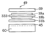
図17は表示構成電極を力測定電極に兼用するタッチパネルを具備する電子機器の断面図である。電子機器49は上下面分極圧電体31bの上側に支持フィルム333、表ガラス39を有する。上下面分極圧電体31bは表示装置60の上に載置されている。
FIG. 17 is a cross-sectional view of an electronic apparatus including a touch panel that also serves as a force measurement electrode as a display constituent electrode. The
表示装置60の表面付近に表示構成電極45が在る。表示構成電極45としては、表示装置60がVA(Vertical Alignment)駆動方式のLCDの場合におけるCOM電極(共通電極)、表示装置60がIPS(In-Place-Switching)駆動方式のLCDの場合におけるチャージ防止電極を例示できる。
The display constituent electrode 45 is present near the surface of the
タッチパネルが力測定を行う時間に、表示構成電極は接地され、接地電極(GND)の役割を担う。支持フィルム333の上表面にTP専用電極である上側電極18aが形成され、支持フィルム333の下表面にTP専用電極である下側電極18bが形成されている。
At the time when the touch panel performs force measurement, the display constituent electrode is grounded and plays the role of a ground electrode (GND). An
タッチパネルにおけるTP専用電極は位置検出用の一双の電極、すなわち受電電極(Rx)と送電電極(Tx)及び力測定用の測定電極(Sx)である。これら3種の電極を任意に1種の電極と2種の電極に分割し、上側電極18aと下側電極18bに割り当てている。従って、上側電極18aに1種又は2種の電極が配置され、下側電極18bに2種又は1種の電極が配置される。
The electrodes dedicated for TP in the touch panel are a pair of electrodes for position detection, that is, a power receiving electrode (Rx), a power transmitting electrode (Tx), and a force measuring measurement electrode (Sx). These three types of electrodes are arbitrarily divided into one type of electrode and two types of electrodes, which are assigned to the
図18はグループ2における好ましいTP専用電極の配置組合せを示す表である。グループ2は上下面分極性圧電体を使用するタッチパネルを用いる点が共通する実施態様である。表中の上側電極と下側電極は両者共に上下面分極圧電体31bよりも上側に位置する。そして2つの電極の相対位置が上側、下側である。
FIG. 18 is a table showing a preferred combination of TP dedicated electrodes in
A5では上側にRx、下側にTxとSxを配置する。力測定の電極対はSxと枠である。 In A5, Rx is arranged on the upper side, and Tx and Sx are arranged on the lower side. The force measurement electrode pair is Sx and a frame.
A6では上側にRx、下側にTxとSxを配置する。力測定の電極対はSxと表示構成電極である。 In A6, Rx is arranged on the upper side, and Tx and Sx are arranged on the lower side. The force measurement electrode pair is Sx and a display component electrode.
A5とA6の配置において、上側電極と下側電極は一枚の支持体の両面に形成することが好ましい。タッチパネルの透明性などの光学特性を良好にするためである。支持体の例は支持フィルム、支持板である。 In the arrangement of A5 and A6, the upper electrode and the lower electrode are preferably formed on both surfaces of a single support. This is to improve the optical characteristics such as transparency of the touch panel. Examples of the support are a support film and a support plate.
導電体パターンを説明する。 The conductor pattern will be described.
図19はTP専用電極を2面に形成した一の導電パターンの平面図である。図19(a)は上側電極の平面図、図19(b)は下側電極の平面図であり、図19(c)は電極投影図である。本実施例はTP専用電極の配置組合せA5に属する。上側電極18aは受電電極(Rx)が配置され、Rxを構成する第一導電体1a、1b、1c、1dが形成されている。第一導電体1は短冊(長方形)形状であり、その長手方向がY軸に平行に配置されている。また第一導電体1a、1b、1c、1dはそれぞれ平行に配置されている。
FIG. 19 is a plan view of one conductive pattern in which TP-dedicated electrodes are formed on two surfaces. 19A is a plan view of the upper electrode, FIG. 19B is a plan view of the lower electrode, and FIG. 19C is an electrode projection view. This embodiment belongs to the arrangement combination A5 of the TP dedicated electrode. A power receiving electrode (Rx) is disposed on the
下側電極18bは送電電極(Tx)と測定電極(Sx)が配置されている。下側電極18bはTxを構成する第二導電体2a、2b、・・・2fが形成され、Sxを構成する第三導電体103が形成されている。第二導電体2は短冊(長方形)形状であり、その長手方向がX軸に平行に配置されている。
The
第三導電体103はその外形が長方形であり、内側は長方形形状に開口している。換言すると第三導電体103は額縁形状である。第三導電体103は支持フィルム上で連続した一体である。また第三導電体103は枠の形状に対応する平面形状である。力測定に使用する一対の電極であるSx(すなわち第三導電体103)とGND(すなわち枠)の平面形状を一致させ、これを対向させることにより力測定の感度が向上する。
The
第三導電体103と第二導電体2a、2b、・・・2fの立体交差面211には絶縁体を挿んでいる。絶縁体は図示を省略した。
An insulator is inserted in the three-
図19(c)は電極投影図20である。位置交差領域21と第三導電体103は電極投影図上で隔離している。このようにして位置検出時における夾雑信号の減少を図っている。
FIG. 19C is an
図20はTP専用電極を2面に形成した他の導電体パターンの平面図である。図20(a)は上側電極の平面図、図20(b)は下側電極の平面図であり、図20(c)は電極投影図である。この実施例はTP専用電極の配置組合せA6に属する。上側電極18aは受電電極(Rx)が配置され、Rxを構成する第一導電体1a、1b、1c、1dが形成されている。第一導電体1は短冊(長方形)形状であり、その長手方向がY軸に平行に配置されている。それぞれの第一導電体1a、1b、1c、1dは互いに平行に配置されている。
FIG. 20 is a plan view of another conductor pattern in which TP-dedicated electrodes are formed on two surfaces. 20A is a plan view of the upper electrode, FIG. 20B is a plan view of the lower electrode, and FIG. 20C is an electrode projection view. This embodiment belongs to the TP-dedicated electrode arrangement combination A6. A power receiving electrode (Rx) is disposed on the
下側電極18bは送電電極(Tx)と測定電極(Sx)が配置されている。下側電極18bはTxを構成する第二導電体2a、2b、・・・2fが形成され、Sxを構成する第三導電体3a、3b、・・・3fが形成されている。第二導電体2は短冊(長方形)形状であり、その長手方向がX軸に平行に配置されている。
The
第三導電体3は概略短冊形状であり、その長手方向がX軸に平行に配置されている。第三導電体3を詳述すれば、長方形の広幅部113と長方形の狭幅部123がX軸方向に交互に連なった形状である。ここで「幅」はY軸方向の両端間の距離である。
The
第二導電体2a、2b、・・・2fと第三導電体3a、3b、・・・3fはY軸方向で交互に配置されている。
The
電極投影図20上で第一導電体1と第二導電体2が交差している。さらに、第一導電体1と第三導電体3が交差している。第三導電体3は狭幅部123で第一導電体1と交差している。第三導電体に設けた広幅部113と狭幅部123により、力測定にあたり圧電体31bに生ずる電圧変化をより高感度に検知でき、同時に位置検出にあたり夾雑信号を抑制できる。
The
広幅部113の形状に制限はなく、いかなる形状であってもよい。図9で説明した導電体パターンの場合と同様である。
There is no restriction | limiting in the shape of the
図21はTP専用電極を2面に形成したさらに他の例にかかる導電体パターンの平面図である。図21(a)は上側電極の平面図、図21(b)は下側電極の平面図であり、図21(c)は電極投影図である。この実施例はTP専用電極の配置組合せA6に属する。 FIG. 21 is a plan view of a conductor pattern according to still another example in which TP-dedicated electrodes are formed on two surfaces. FIG. 21A is a plan view of the upper electrode, FIG. 21B is a plan view of the lower electrode, and FIG. 21C is an electrode projection view. This embodiment belongs to the TP-dedicated electrode arrangement combination A6.
上側電極18aは受電電極(Rx)が配置され、Rxを構成する第一導電体1a、1b、1c、1dが形成されている。第一導電体1については、図20で説明した導電体パターンと同一である。
A power receiving electrode (Rx) is disposed on the
下側電極18bは送電電極(Tx)と測定電極(Sx)が配置されている。下側電極18bはTxを構成する第二導電体2a、2b、・・・2fが形成され、Sxを構成する第三導電体3a、3b、・・・3fが形成されている。第二導電体2は短冊(長方形)形状であり、その長手方向がX軸に平行に配置されている。
The
第三導電体3は概略短冊形状であり、その長手方向がY軸に平行に配置されている。第三導電体3を詳述すれば、長方形の広幅部113と長方形の狭幅部123がY軸方向に交互に連なった形状である。
The
第三導電体3a、3b、・・・3fと第二導電体2a、2b、・・・2fの立体交差面211には絶縁体を挿んでいる。絶縁体は図示を省略した。第三導電体3に広幅部113と狭幅部123を設けたので、圧電体31bに生じる電圧変化をより高感度に検知できる。また、位置交差領域21と第三導電体3a、3b、・・・3fを離隔したので、位置検出時の夾雑信号を抑制できる。
An insulator is inserted in the three-
続いて、第一グループと第二グループに属する実施態様に共通する事項を説明する。まず。タッチパネルの位置検出方法と力測定方法を説明する。 Subsequently, matters common to the embodiments belonging to the first group and the second group will be described. First. A touch panel position detection method and force measurement method will be described.
図22は力測定に使用する測定電極(Sx)と接地電極(GND)を備え、位置検出に使用する受電電極(Rx)と送電電極(Tx)を備えるタッチパネルの回路説明図である。 FIG. 22 is a circuit explanatory diagram of a touch panel including a measurement electrode (Sx) and a ground electrode (GND) used for force measurement, and a power reception electrode (Rx) and a power transmission electrode (Tx) used for position detection.
送電電極(Tx)12と受電電極(Rx)11はマトリックス検出回路37に接続される。マトリックス検出回路37は公知の静電容量方式の投影型の検出回路でありタッチパネル上の押圧位置が検出される。測定電極(Sx)13はチャージアンプ35に接続される。接地電極(GND)14は接地される。
The power transmission electrode (Tx) 12 and the power reception electrode (Rx) 11 are connected to the
押圧により圧電体に生じ測定電極(Sx)で検出される電荷は、チャージアンプ35で電圧の値として測定される。当該測定電圧値は押圧力を示す値である。
The charge generated in the piezoelectric body by the pressing and detected by the measurement electrode (Sx) is measured by the
図23は力測定に使用する測定電極(Sx)を備え、位置検出に使用する受電電極(Rx)と送電電極(Tx)を備えるタッチパネルの回路説明図である。送電電極(Tx)12と受電電極(Rx)11はマトリックス検出回路37に接続される。位置検出時にはスイッチ36が開となり、送電電極(Tx)12は接地から離れている。
FIG. 23 is a circuit explanatory diagram of a touch panel including a measurement electrode (Sx) used for force measurement and a power reception electrode (Rx) and a power transmission electrode (Tx) used for position detection. The power transmission electrode (Tx) 12 and the power reception electrode (Rx) 11 are connected to the
マトリックス検出回路37による押圧位置検出は図8で説明したタッチパネルと同一である。測定電極(Sx)13はチャージアンプ35に接続される。力測定時にスイッチ36が閉となり送電電極(Tx)12が接地される。この状態で送電電極12は接地電極の役割をはたす。チャージアンプ35による電圧の測定は図22で説明したタッチパネルと同一である。
The pressing position detection by the
続いて、圧電板に位相差板の性質を付与したタッチパネル、当該タッチパネルと表示装置からなる電子機器を説明する。 Next, a touch panel in which the properties of a retardation plate are imparted to a piezoelectric plate, and an electronic device including the touch panel and a display device will be described.
図24は電子機器461の説明図である。電子機器461はLCD600とタッチパネルからなる。LCD600は表示装置である。タッチパネルは圧電体311を含むタッチパネルである。力測定に用いる電極、位置検出に用いる電極等は図示を省略している。
FIG. 24 is an explanatory diagram of the
LCD600は光源68、下偏光板62、液晶セル67と上偏光板61からなり、可視光である出射光92を出射する。図中にX軸方向を破線矢印51、Y軸方向を破線矢印52で示している。Z軸方向は出射光92の進行方向である。
The
上偏光板61の吸収軸611はY軸と平行である。出射光92は直線偏光である。もし、出射光92を、偏光サングラス91を通して目94で見たとするならば、なおかつ偏光サングラス91をXY平面内で回転させるならば、回転途中のある点で表示が見えなくなる(ブラックアウト)。
The
電子機器461は、位相差板としての性質を兼ね備えた圧電体311を採用してブラックアウトを解消している。出射光92の振動面はXZ平面に平行である。当該振動面を圧電体311の表面に投影した線分を振動線921で示している。出射光92の振動面と圧電体311の遅相軸312(位相差板の光学軸とも呼ぶ)が作る角度は、振動線921と遅相軸312が作る角度と等しい。当該角度を角度313で示している。
The
圧電体311の遅相軸312(位相差板の光学軸とも呼ぶ)と出射光92の振動面が作る角度(角度313と等しい)は、通常20度から70度の角度、好ましくは35度から55度の角度に配置される。この角度に配置して、直線偏光の偏光状態を適切に変化させるためである。
The angle formed by the slow axis 312 (also referred to as the optical axis of the phase difference plate) of the
角度313は面と線交差して作る角度のうちで、角度の数値が小さいほうを採用する。
Of the angles formed by crossing the surface, the
出射光92は圧電体311を通過すると、円偏光、楕円偏光等の変換光93に変換される。変換光93は偏光サングラス91を通して目94で観察してもブラックアウトを生じない。
When the outgoing light 92 passes through the
圧電体に位相差板の性質を付与するには、圧電体をフィルム形状にして、当該フィルム状圧電体を一軸延伸すればよい。通常、一軸延伸の操作を加えた後に、分極操作用の電圧を負荷する分極操作を行う。 In order to impart the properties of the retardation plate to the piezoelectric body, the piezoelectric body may be formed into a film shape and the film-like piezoelectric body may be uniaxially stretched. Usually, after applying a uniaxial stretching operation, a polarization operation is performed by applying a voltage for the polarization operation.
圧電体311のリタデーション値は(1)110nm以上170nm以下、または(2)800nm以上30,000nm以下のいずれかにする。当該値を(1)110nm以下170nm以下の範囲にすれば、可視光の波長領域中で特定波長の直線偏光の光が円偏光に変換され、その他の波長の同様の光が楕円偏光に変換される。また当該値を(2)800nm以上30,000nm以下の範囲にすれば、可視光の波長領域中で複数の特定波長の直線偏光の光が円偏光に変換され、その他の波長の同様の光が楕円偏光に変換される。
The retardation value of the
また圧電体311のリタデーション値は、出射光92の波長λ(ラムダ)の(1/4+K/2)倍の値(Kは0又は正の整数)であってもよい。
Further, the retardation value of the
図25は電子機器462の説明図である。電子機器462はOLED70とタッチパネルからなる。OLED70は表示装置である。タッチパネルは圧電体311を含むタッチパネルである。力測定に用いる電極、位置検出に用いる電極等は図示を省略している。
FIG. 25 is an explanatory diagram of the
OLED70は発光セル77、偏光板71からなり可視光である出射光92を出射する。
The
図中にX軸方向を破線矢印51、Y軸方向を破線矢印52で示している。Z軸方向は出射光92の進行方向である。
In the figure, the X-axis direction is indicated by a
偏光板71の吸収軸711はY軸と平行である。出射光92は直線偏光であり、その振動面はY軸に平行である。圧電体311は位相差板としての性質を兼ね備えている。
The
遅相軸312と出射光92の振動面との角度313は電子機器461の場合と同一である。
An
圧電体に位相差板としての性質を付与する方法、圧電体のリタデーション値の範囲、これらの効果も電子機器461で説明したことと同一である。
The method of imparting properties as a retardation plate to the piezoelectric body, the range of the retardation value of the piezoelectric body, and these effects are the same as those described in the
XY平面分極圧電体31aと上下面分極圧電体31b(以下両者を合わせて圧電体31と称する)は板状であり、その厚さは1μm〜200μmである。圧電体31を構成する材料としては、セラミック圧電材料、フッ化物重合体、またはその共重合体、さらには、キラリティーを有する高分子材料などが挙げられる。セラミック圧電材料としては、チタン酸バリウム、チタン酸鉛、チタン酸ジルコン酸鉛、ニオブ酸カリウム、ニオブ酸リチウム、タンタル酸リチウム、タングステン酸ナトリウム、酸化亜鉛、ニオブ酸ナトリウムカリウム、ビスマスフェライト、ニオブ酸ナトリウム、チタン酸ビスマスなどが挙げられる。フッ化物重合体、またはその共重合体としては、ポリフッ化ビニリデン、フッ化ビニリデン−テトラフルオロエチレン共重合体、フッ化ビニリデン−トリフルオロエチレン共重合体が挙げられる。キラリティーを有する高分子材料としては、L型ポリ乳酸や、R型ポリ乳酸などが挙げられる。
The XY plane polarization
支持フィルムは、例えばポリエチレンテレフタラート(PET)樹脂で作られる。 The support film is made of, for example, polyethylene terephthalate (PET) resin.
上面電極16と下面電極17は公知の透明な導電材料で作られる。例えば、ITO膜、TZO膜などである。また、PEDOTのような導電性高分子を含有したインキや金属ナノファイバーが含有されたインキを用いて印刷して形成してもよい。さらに、タッチパネルに透明性が求められない場合は、金属箔、金属ペースト、カーボンペーストを用いて印刷形成してもよい。 The upper electrode 16 and the lower electrode 17 are made of a known transparent conductive material. For example, an ITO film or a TZO film. Further, it may be formed by printing using an ink containing a conductive polymer such as PEDOT or an ink containing metal nanofibers. Furthermore, when transparency is not required for the touch panel, printing may be performed using a metal foil, a metal paste, or a carbon paste.
電極形成は例えばスパッタリングで行ってもよく、印刷してもよい。さらには、銅などからなる金属箔を接着剤で貼り合わせてもよいし、メッキ法により形成してもよい。 The electrode formation may be performed by sputtering or printing, for example. Furthermore, a metal foil made of copper or the like may be bonded with an adhesive, or may be formed by a plating method.
電子機器は、携帯電話機、デジタルカメラ、券売機、金融機関のATM等に使用することができる。 The electronic device can be used for cellular phones, digital cameras, ticket machines, ATMs of financial institutions, and the like.
力測定の感度を上げるために、タッチパネル40と表示装置60の間に複数の突起物(バンプ)を配置してもよい。バンプを形成すれば、指でタッチパネルを押下したときにタッチパネルがより大きく撓むため、力検出の感度が向上する。
In order to increase the sensitivity of force measurement, a plurality of protrusions (bumps) may be disposed between the
また、タッチパネル40と表示装置60のいずれか少なくとも一方にはAR処理が施されていてもよい。さらには、タッチパネル40と表示装置60の間にAR処理が施されたフィルムなどが配置されていてもよい。AR処理とは、基材の表面にシリカやフッ化物からなる無機薄膜や、フッ素樹脂等からなる有機薄膜を形成したり、基材の表面にナノ〜サブミクロンオーダの凹凸を形成したりする処理のことである。上記のような処理を施すと、タッチパネルの表面反射やディスプレイの表面反射を抑えることができる。上面電極16の上に表面部材33が重ねられている。表面部材33としては、例えば、ソーダガラス、無アルカリガラス、ホウケイ酸ガラス、石英ガラス等の各種ガラス材料や、ポリイミド系樹脂、アクリル系樹脂、ポリエステル系樹脂、ポリカーボネート系樹脂等の各種樹脂材料で構成されたものを用いることができる。
Further, at least one of the
本発明のその他の態様にかかる電子機器は、
表示装置とタッチパネルからなる電子機器であって、前記タッチパネルは圧電体を使用し押圧力である力を測定する力測定と前記タッチパネルが押圧された位置を検出する投影型静電容量方式の位置検出を備えたタッチパネルである電子機器において、
表示装置の表示面を構成している表面部材に重ねて板状のタッチパネルが配置されていて、前記タッチパネルは板状の圧電体とTP専用電極からなり、前記圧電体の板状面がXY平面に平行な面であり、前記表面部材と前記タッチパネルの重なり方向が上下方向であって、前記タッチパネル方向を上側として、
位置検出は、一双の電極を使用するものであって、前記一双の電極のうち一の電極はXY平面上の一の方向に平行に配置された一群の導電体からなり、前記一双の電極のうち他の電極はXY平面上で前記一の方向と交差する方向に平行に配置された一群の他の導電体からなり、
力測定は電極を使用して前記圧電体に押圧力である力が負荷されたときに前記圧電体に生じる電力を測定するものであり、
前記TP専用電極は、力測定のみに使用する電極、位置検出のみに使用する電極及び力測定と位置検出を兼用しこれらのみに使用する電極であり、
前記圧電体の上面側に前記TP専用電極が配置され、前記圧電体の下面は直接前記表面部材と接しているか、又は、前記圧電体の下面は電気絶縁性の部材を介在して前記表面部材と接している電子機器である。
An electronic device according to another aspect of the present invention includes:
An electronic apparatus comprising a display device and a touch panel, wherein the touch panel uses a piezoelectric body to measure force that is a pressing force and a projected capacitive type position detection that detects a position where the touch panel is pressed In an electronic device that is a touch panel equipped with
A plate-shaped touch panel is disposed on a surface member constituting the display surface of the display device, and the touch panel includes a plate-shaped piezoelectric body and a TP dedicated electrode, and the plate-shaped surface of the piezoelectric body is an XY plane. The overlapping direction of the surface member and the touch panel is the vertical direction, and the touch panel direction is the upper side,
The position detection uses a pair of electrodes, and one electrode of the pair of electrodes is composed of a group of conductors arranged in parallel in one direction on the XY plane. The other electrode is composed of a group of other conductors arranged parallel to the direction intersecting the one direction on the XY plane,
Force measurement is to measure the electric power generated in the piezoelectric body when a force that is a pressing force is applied to the piezoelectric body using an electrode,
The electrode dedicated to TP is an electrode used only for force measurement, an electrode used only for position detection, and an electrode used only for force measurement and position detection.
The TP-dedicated electrode is disposed on the upper surface side of the piezoelectric body, and the lower surface of the piezoelectric body is in direct contact with the surface member, or the lower surface of the piezoelectric body is interposed with an electrically insulating member in the surface member. Is an electronic device in contact with
以上本発明にかかる複数の実施の形態について図面を参照して詳述してきたが、具体的な構成例はこれらの実施の形態に限られるものではなく、本発明の要旨を逸脱しない範囲の設計変更などがあっても本発明に含まれる。 Although a plurality of embodiments according to the present invention have been described in detail with reference to the drawings, specific configuration examples are not limited to these embodiments, and the design does not depart from the gist of the present invention. Any changes are included in the present invention.
1 第一導電体
2 第二導電体
3 第三導電体
103 枠に対応する第三導電体
4 第四導電体
11 位置検出に用いる一の電極又は他の電極である受電電極(Rx)
12 位置検出に用いる一の電極又は他の電極である送電電極(Tx)
13 力測定に使用する一対の電極の一電極である測定電極(Sx)
14 力測定に使用する一対の電極の一電極である接地電極(GND)
18a 上側電極(TP専用電極)
18b 下側電極(TP専用電極)
18c 一層TP専用電極(TP専用電極)
20 電極投影図
21 位置交差領域
22、23 分極操作用電極
24 直流電源
25 電圧計
26 圧電材料(分極操作前)
27 押圧力を示す矢印
31 圧電体
31a XY平面分極圧電体
31b 上下面分極圧電体
331、332、333 支持フィルム
35 チャージアンプ
36 スイッチ
37 マトリックス検出回路
38 接着剤
39 表ガラス
40 タッチパネル
41 枠を電極とするタッチパネル
44 枠
45 表示構成電極
46 電子機器
47 タッチパネル(XY平面分極圧電体を使用)
49 表示構成電極を兼用するタッチパネルを使用する電子機器
51 X軸を示す矢印
52 Y軸を示す矢印
53 上方向を示す矢印
60 表示装置
67 液晶セル
70 OLED
71 偏光板
77 発光セル
91 偏光サングラス
92 出射光
93 変換光
94 観察位置である目
103 枠に対応する第三導電体
113 広幅部
123 狭幅部
211 立体交差面
311 位相差板である圧電体
312 遅相軸
313 角度
461 電子機器
462 電子機器
600 LCD
611 吸収軸
711 吸収軸
921 (出射光92の振動面を圧電体311の表面に投影した線分である)振動線
DESCRIPTION OF
12 Power transmission electrode (Tx) which is one electrode or another electrode used for position detection
13 Measuring electrode (Sx) which is one electrode of a pair of electrodes used for force measurement
14 Ground electrode (GND) which is one electrode of a pair of electrodes used for force measurement
18a Upper electrode (TP dedicated electrode)
18b Lower electrode (TP dedicated electrode)
18c Single layer TP electrode (TP electrode)
20
27 Arrows indicating pressing
49 Electronic equipment using a touch panel that also serves as a
DESCRIPTION OF
611
Claims (11)
前記タッチパネルは圧電体と前記圧電体の上面側に位置付けられたTP専用電極からなり、
力検出は電極を使用して前記圧電体に力が負荷されたときに前記圧電体に生じる電力を測定するものであり、
位置検出は一組の電極を使用するものであり、前記一組の電極のうち一の電極はXY平面上の一の方向に平行に配置された一群の導電体からなり、他の電極は前記一の方向と交差する方向に平行に配置された一群の他の導電体からなり、
前記TP専用電極とは、力検出に使用する電極、位置検出に使用する電極及び/または力検出と位置検出を兼用する電極を意味するものであって、
前記圧電体は、力を受けるとXY平面に平行な面内で電荷が発生するXY平面分極性圧電体であるタッチパネル。 A projection capacitive touch panel having a force detection for detecting force using a piezoelectric body and a position detection for detecting a position, wherein the touch panel is dedicated to a TP positioned on the upper surface side of the piezoelectric body and the piezoelectric body. Consisting of electrodes,
Force detection is to measure the electric power generated in the piezoelectric body when a force is applied to the piezoelectric body using an electrode,
The position detection uses a set of electrodes, and one electrode of the set of electrodes is composed of a group of conductors arranged in parallel in one direction on the XY plane, and the other electrodes are the above-described electrodes. Consisting of a group of other conductors arranged parallel to a direction intersecting one direction,
Wherein the TP dedicated electrode, the electrode for use in a force detection, I der shall mean an electrode that also functions as a position detection and electrodes and / or force detection is used to detect position,
The touch panel is an XY plane polarizable piezoelectric body that generates charges in a plane parallel to the XY plane when receiving force .
前記圧電体は位相差板であって前記圧電体である位相差板の遅相軸が、前記直線偏光の振動面に対して20度から70度の角度で配置して用いられる請求項1乃至3いずれかに記載したタッチパネル。 The touch panel is a touch panel used by being placed on a display surface of a display device, and the display device has visible light emitted from the display surface as linearly polarized light,
The piezoelectric body is the slow axis of the retardation plate is a piezoelectric a retardation plate, 1 to claim is used in place at an angle of 70 degrees from 20 degrees relative to the plane of vibration of the linearly polarized light 3 Touch panel described in any one.
前記圧電体は位相差板であって前記圧電体のリタデーション値が110nm以上170nm以下である請求項1乃至4いずれかに記載したタッチパネル。 The touch panel is a touch panel used by being placed on a display surface of a display device, and the display device has visible light emitted from the display surface as linearly polarized light,
The piezoelectric body is a touch panel as claimed in any one of claims 1 to 4 retardation value of the piezoelectric a retardation plate is 110nm or more 170nm or less.
前記圧電体は位相差板であって前記圧電体のリタデーション値が800nm以上30,000nm以下である請求項1乃至4いずれかに記載したタッチパネル。 The touch panel is a touch panel used by being placed on a display surface of a display device, and the display device has visible light emitted from the display surface as linearly polarized light,
The piezoelectric body is a touch panel as claimed in any one of claims 1 to 4 retardation value of the piezoelectric a retardation plate is 800nm or more 30,000nm or less.
力検出に使用する一対の電極は測定電極と接地電極であり、
前記測定電極は一群の導電体である第三導電体から構成されていて、
前記TP専用電極を一のXY平面である仮想平面に投影した電極投影図上で、第三導電体は第一導電体又は第二導電体のいずれかと平行に配置されていて、第一導電体と第二導電体の交差領域を位置交差領域としたとき、前記位置交差領域と第三導電体が離隔している請求項1乃至3いずれかに記載したタッチパネル。 Among a set of electrodes used for position detection, a group of conductors constituting one electrode is a first conductor, a group of other conductors constituting another electrode is a second conductor,
A pair of electrodes used for force detection is a measurement electrode and a ground electrode,
The measurement electrode is composed of a third conductor which is a group of conductors,
The third conductor is arranged in parallel with either the first conductor or the second conductor on the electrode projection view in which the TP-dedicated electrode is projected onto a virtual plane that is one XY plane, and the first conductor when the second conductor crossing area when the position intersecting regions, the touch panel as claimed in any one of claims 1 to 3 wherein the position intersecting region and the third conductor are spaced apart.
前記電極投影図上で、前記狭幅部が第二導電体と交差する請求項7に記載したタッチパネル。 The third conductor has continuous wide and narrow portions alternately,
The touch panel according to claim 7 , wherein the narrow portion intersects the second conductor on the electrode projection view.
Priority Applications (1)
| Application Number | Priority Date | Filing Date | Title |
|---|---|---|---|
| JP2013110655A JP6151970B2 (en) | 2013-03-28 | 2013-05-27 | Touch panel with pressure measurement |
Applications Claiming Priority (3)
| Application Number | Priority Date | Filing Date | Title |
|---|---|---|---|
| JP2013067701 | 2013-03-28 | ||
| JP2013067701 | 2013-03-28 | ||
| JP2013110655A JP6151970B2 (en) | 2013-03-28 | 2013-05-27 | Touch panel with pressure measurement |
Publications (3)
| Publication Number | Publication Date |
|---|---|
| JP2014209297A JP2014209297A (en) | 2014-11-06 |
| JP2014209297A5 JP2014209297A5 (en) | 2016-04-14 |
| JP6151970B2 true JP6151970B2 (en) | 2017-06-21 |
Family
ID=51903493
Family Applications (1)
| Application Number | Title | Priority Date | Filing Date |
|---|---|---|---|
| JP2013110655A Expired - Fee Related JP6151970B2 (en) | 2013-03-28 | 2013-05-27 | Touch panel with pressure measurement |
Country Status (1)
| Country | Link |
|---|---|
| JP (1) | JP6151970B2 (en) |
Families Citing this family (12)
| Publication number | Priority date | Publication date | Assignee | Title |
|---|---|---|---|---|
| GB2533667B (en) | 2014-12-23 | 2017-07-19 | Cambridge Touch Tech Ltd | Pressure-sensitive touch panel |
| JP6712597B2 (en) | 2014-12-23 | 2020-06-24 | ケンブリッジ タッチ テクノロジーズ リミテッドCambridge Touch Technologies Limited | Pressure sensitive touch panel |
| JP6441168B2 (en) | 2015-05-29 | 2018-12-19 | 株式会社ジャパンディスプレイ | Display device with sensor |
| GB2544353B (en) | 2015-12-23 | 2018-02-21 | Cambridge Touch Tech Ltd | Pressure-sensitive touch panel |
| US10282046B2 (en) | 2015-12-23 | 2019-05-07 | Cambridge Touch Technologies Ltd. | Pressure-sensitive touch panel |
| KR101696445B1 (en) * | 2016-03-10 | 2017-01-16 | 주식회사 베프스 | Apparatus and method for scanning biometric information using pressing-point as a reference |
| JP6714959B2 (en) | 2016-12-28 | 2020-07-01 | アルプスアルパイン株式会社 | Input device |
| US11093088B2 (en) | 2017-08-08 | 2021-08-17 | Cambridge Touch Technologies Ltd. | Device for processing signals from a pressure-sensing touch panel |
| GB2565305A (en) | 2017-08-08 | 2019-02-13 | Cambridge Touch Tech Ltd | Device for processing signals from a pressure-sensing touch panel |
| KR102464258B1 (en) * | 2018-03-06 | 2022-11-08 | 삼성디스플레이 주식회사 | Touch sensor and display device including the same |
| GB2580700B (en) | 2019-01-25 | 2021-06-09 | Cambridge Touch Tech Ltd | Touch panel for combined capacitive touch and force sensing |
| GB2581495A (en) | 2019-02-19 | 2020-08-26 | Cambridge Touch Tech Ltd | Force sensing touch panel |
Family Cites Families (2)
| Publication number | Priority date | Publication date | Assignee | Title |
|---|---|---|---|---|
| JP5526761B2 (en) * | 2009-12-22 | 2014-06-18 | ソニー株式会社 | Sensor device and information processing device |
| CN103858079B (en) * | 2011-08-11 | 2016-12-14 | 株式会社村田制作所 | Touch panel |
-
2013
- 2013-05-27 JP JP2013110655A patent/JP6151970B2/en not_active Expired - Fee Related
Also Published As
| Publication number | Publication date |
|---|---|
| JP2014209297A (en) | 2014-11-06 |
Similar Documents
| Publication | Publication Date | Title |
|---|---|---|
| JP6151970B2 (en) | Touch panel with pressure measurement | |
| JP5855604B2 (en) | Touch panel with pressure measurement | |
| US9990099B2 (en) | Display device | |
| JP5871111B1 (en) | Touch panel and electronic equipment | |
| US9519378B2 (en) | Pressure detector and touch panel provided with pressure detector | |
| KR101631116B1 (en) | Pressure sensing display device and electronic device | |
| US10175831B2 (en) | Display device with a capacitive touch panel | |
| JP5896692B2 (en) | Input display device | |
| WO2012046702A1 (en) | Display device, and process for manufacturing display device | |
| CN109196452A (en) | touch sensor | |
| US10528202B2 (en) | Piezoelectric sensor, touch panel, touch input device, and display device | |
| US10481732B2 (en) | Press detecting touch panel and display device | |
| WO2016103997A1 (en) | Touch panel | |
| US20190235686A1 (en) | Pressure sensor and display device | |
| JP2016143198A (en) | Display device |
Legal Events
| Date | Code | Title | Description |
|---|---|---|---|
| A521 | Request for written amendment filed |
Free format text: JAPANESE INTERMEDIATE CODE: A523 Effective date: 20160226 |
|
| A621 | Written request for application examination |
Free format text: JAPANESE INTERMEDIATE CODE: A621 Effective date: 20160226 |
|
| A977 | Report on retrieval |
Free format text: JAPANESE INTERMEDIATE CODE: A971007 Effective date: 20161227 |
|
| A131 | Notification of reasons for refusal |
Free format text: JAPANESE INTERMEDIATE CODE: A131 Effective date: 20170110 |
|
| A521 | Request for written amendment filed |
Free format text: JAPANESE INTERMEDIATE CODE: A523 Effective date: 20170303 |
|
| A131 | Notification of reasons for refusal |
Free format text: JAPANESE INTERMEDIATE CODE: A131 Effective date: 20170314 |
|
| A521 | Request for written amendment filed |
Free format text: JAPANESE INTERMEDIATE CODE: A523 Effective date: 20170407 |
|
| TRDD | Decision of grant or rejection written | ||
| A01 | Written decision to grant a patent or to grant a registration (utility model) |
Free format text: JAPANESE INTERMEDIATE CODE: A01 Effective date: 20170523 |
|
| A61 | First payment of annual fees (during grant procedure) |
Free format text: JAPANESE INTERMEDIATE CODE: A61 Effective date: 20170526 |
|
| R150 | Certificate of patent or registration of utility model |
Ref document number: 6151970 Country of ref document: JP Free format text: JAPANESE INTERMEDIATE CODE: R150 |
|
| S533 | Written request for registration of change of name |
Free format text: JAPANESE INTERMEDIATE CODE: R313533 |
|
| R350 | Written notification of registration of transfer |
Free format text: JAPANESE INTERMEDIATE CODE: R350 |
|
| R250 | Receipt of annual fees |
Free format text: JAPANESE INTERMEDIATE CODE: R250 |
|
| R250 | Receipt of annual fees |
Free format text: JAPANESE INTERMEDIATE CODE: R250 |
|
| LAPS | Cancellation because of no payment of annual fees |