JP6143601B2 - Image display device - Google Patents
Image display device Download PDFInfo
- Publication number
- JP6143601B2 JP6143601B2 JP2013162682A JP2013162682A JP6143601B2 JP 6143601 B2 JP6143601 B2 JP 6143601B2 JP 2013162682 A JP2013162682 A JP 2013162682A JP 2013162682 A JP2013162682 A JP 2013162682A JP 6143601 B2 JP6143601 B2 JP 6143601B2
- Authority
- JP
- Japan
- Prior art keywords
- phase shift
- light
- image display
- axis
- vcsel
- Prior art date
- Legal status (The legal status is an assumption and is not a legal conclusion. Google has not performed a legal analysis and makes no representation as to the accuracy of the status listed.)
- Active
Links
- 230000010363 phase shift Effects 0.000 claims description 82
- 239000013078 crystal Substances 0.000 claims description 22
- 238000000034 method Methods 0.000 claims description 8
- 230000001427 coherent effect Effects 0.000 claims description 6
- 239000011159 matrix material Substances 0.000 claims description 6
- 239000004973 liquid crystal related substance Substances 0.000 claims description 3
- 239000011295 pitch Substances 0.000 description 23
- 230000003287 optical effect Effects 0.000 description 7
- 238000003491 array Methods 0.000 description 6
- 230000008859 change Effects 0.000 description 5
- 210000000695 crystalline len Anatomy 0.000 description 5
- 239000003990 capacitor Substances 0.000 description 3
- 230000007423 decrease Effects 0.000 description 3
- 239000000835 fiber Substances 0.000 description 3
- 230000004907 flux Effects 0.000 description 3
- 210000001525 retina Anatomy 0.000 description 3
- 210000005252 bulbus oculi Anatomy 0.000 description 2
- 239000003086 colorant Substances 0.000 description 2
- 238000010586 diagram Methods 0.000 description 2
- GQYHUHYESMUTHG-UHFFFAOYSA-N lithium niobate Chemical compound [Li+].[O-][Nb](=O)=O GQYHUHYESMUTHG-UHFFFAOYSA-N 0.000 description 2
- 210000001747 pupil Anatomy 0.000 description 2
- 206010020675 Hypermetropia Diseases 0.000 description 1
- ZLMJMSJWJFRBEC-UHFFFAOYSA-N Potassium Chemical compound [K] ZLMJMSJWJFRBEC-UHFFFAOYSA-N 0.000 description 1
- 230000002411 adverse Effects 0.000 description 1
- 238000013459 approach Methods 0.000 description 1
- 230000008901 benefit Effects 0.000 description 1
- 230000005540 biological transmission Effects 0.000 description 1
- 238000002425 crystallisation Methods 0.000 description 1
- 230000008025 crystallization Effects 0.000 description 1
- 230000000694 effects Effects 0.000 description 1
- 238000012986 modification Methods 0.000 description 1
- 230000004048 modification Effects 0.000 description 1
- 229910052700 potassium Inorganic materials 0.000 description 1
- 239000011591 potassium Substances 0.000 description 1
- 229910052710 silicon Inorganic materials 0.000 description 1
- 239000010703 silicon Substances 0.000 description 1
- 230000001360 synchronised effect Effects 0.000 description 1
- 239000010409 thin film Substances 0.000 description 1
Images


Classifications
-
- H—ELECTRICITY
- H04—ELECTRIC COMMUNICATION TECHNIQUE
- H04N—PICTORIAL COMMUNICATION, e.g. TELEVISION
- H04N9/00—Details of colour television systems
- H04N9/12—Picture reproducers
- H04N9/31—Projection devices for colour picture display, e.g. using electronic spatial light modulators [ESLM]
- H04N9/3129—Projection devices for colour picture display, e.g. using electronic spatial light modulators [ESLM] scanning a light beam on the display screen
-
- G—PHYSICS
- G02—OPTICS
- G02F—OPTICAL DEVICES OR ARRANGEMENTS FOR THE CONTROL OF LIGHT BY MODIFICATION OF THE OPTICAL PROPERTIES OF THE MEDIA OF THE ELEMENTS INVOLVED THEREIN; NON-LINEAR OPTICS; FREQUENCY-CHANGING OF LIGHT; OPTICAL LOGIC ELEMENTS; OPTICAL ANALOGUE/DIGITAL CONVERTERS
- G02F1/00—Devices or arrangements for the control of the intensity, colour, phase, polarisation or direction of light arriving from an independent light source, e.g. switching, gating or modulating; Non-linear optics
- G02F1/29—Devices or arrangements for the control of the intensity, colour, phase, polarisation or direction of light arriving from an independent light source, e.g. switching, gating or modulating; Non-linear optics for the control of the position or the direction of light beams, i.e. deflection
- G02F1/292—Devices or arrangements for the control of the intensity, colour, phase, polarisation or direction of light arriving from an independent light source, e.g. switching, gating or modulating; Non-linear optics for the control of the position or the direction of light beams, i.e. deflection by controlled diffraction or phased-array beam steering
-
- H—ELECTRICITY
- H01—ELECTRIC ELEMENTS
- H01S—DEVICES USING THE PROCESS OF LIGHT AMPLIFICATION BY STIMULATED EMISSION OF RADIATION [LASER] TO AMPLIFY OR GENERATE LIGHT; DEVICES USING STIMULATED EMISSION OF ELECTROMAGNETIC RADIATION IN WAVE RANGES OTHER THAN OPTICAL
- H01S5/00—Semiconductor lasers
- H01S5/005—Optical components external to the laser cavity, specially adapted therefor, e.g. for homogenisation or merging of the beams or for manipulating laser pulses, e.g. pulse shaping
- H01S5/0071—Optical components external to the laser cavity, specially adapted therefor, e.g. for homogenisation or merging of the beams or for manipulating laser pulses, e.g. pulse shaping for beam steering, e.g. using a mirror outside the cavity to change the beam direction
-
- H—ELECTRICITY
- H04—ELECTRIC COMMUNICATION TECHNIQUE
- H04N—PICTORIAL COMMUNICATION, e.g. TELEVISION
- H04N9/00—Details of colour television systems
- H04N9/12—Picture reproducers
- H04N9/31—Projection devices for colour picture display, e.g. using electronic spatial light modulators [ESLM]
- H04N9/3102—Projection devices for colour picture display, e.g. using electronic spatial light modulators [ESLM] using two-dimensional electronic spatial light modulators
-
- G—PHYSICS
- G02—OPTICS
- G02F—OPTICAL DEVICES OR ARRANGEMENTS FOR THE CONTROL OF LIGHT BY MODIFICATION OF THE OPTICAL PROPERTIES OF THE MEDIA OF THE ELEMENTS INVOLVED THEREIN; NON-LINEAR OPTICS; FREQUENCY-CHANGING OF LIGHT; OPTICAL LOGIC ELEMENTS; OPTICAL ANALOGUE/DIGITAL CONVERTERS
- G02F1/00—Devices or arrangements for the control of the intensity, colour, phase, polarisation or direction of light arriving from an independent light source, e.g. switching, gating or modulating; Non-linear optics
- G02F1/29—Devices or arrangements for the control of the intensity, colour, phase, polarisation or direction of light arriving from an independent light source, e.g. switching, gating or modulating; Non-linear optics for the control of the position or the direction of light beams, i.e. deflection
- G02F1/291—Two-dimensional analogue deflection
-
- G—PHYSICS
- G02—OPTICS
- G02F—OPTICAL DEVICES OR ARRANGEMENTS FOR THE CONTROL OF LIGHT BY MODIFICATION OF THE OPTICAL PROPERTIES OF THE MEDIA OF THE ELEMENTS INVOLVED THEREIN; NON-LINEAR OPTICS; FREQUENCY-CHANGING OF LIGHT; OPTICAL LOGIC ELEMENTS; OPTICAL ANALOGUE/DIGITAL CONVERTERS
- G02F2203/00—Function characteristic
- G02F2203/34—Colour display without the use of colour mosaic filters
-
- H—ELECTRICITY
- H01—ELECTRIC ELEMENTS
- H01L—SEMICONDUCTOR DEVICES NOT COVERED BY CLASS H10
- H01L27/00—Devices consisting of a plurality of semiconductor or other solid-state components formed in or on a common substrate
- H01L27/14—Devices consisting of a plurality of semiconductor or other solid-state components formed in or on a common substrate including semiconductor components sensitive to infrared radiation, light, electromagnetic radiation of shorter wavelength or corpuscular radiation and specially adapted either for the conversion of the energy of such radiation into electrical energy or for the control of electrical energy by such radiation
- H01L27/144—Devices controlled by radiation
- H01L27/146—Imager structures
- H01L27/14601—Structural or functional details thereof
- H01L27/1462—Coatings
- H01L27/14623—Optical shielding
-
- H—ELECTRICITY
- H01—ELECTRIC ELEMENTS
- H01S—DEVICES USING THE PROCESS OF LIGHT AMPLIFICATION BY STIMULATED EMISSION OF RADIATION [LASER] TO AMPLIFY OR GENERATE LIGHT; DEVICES USING STIMULATED EMISSION OF ELECTROMAGNETIC RADIATION IN WAVE RANGES OTHER THAN OPTICAL
- H01S5/00—Semiconductor lasers
- H01S5/005—Optical components external to the laser cavity, specially adapted therefor, e.g. for homogenisation or merging of the beams or for manipulating laser pulses, e.g. pulse shaping
- H01S5/0085—Optical components external to the laser cavity, specially adapted therefor, e.g. for homogenisation or merging of the beams or for manipulating laser pulses, e.g. pulse shaping for modulating the output, i.e. the laser beam is modulated outside the laser cavity
-
- H—ELECTRICITY
- H01—ELECTRIC ELEMENTS
- H01S—DEVICES USING THE PROCESS OF LIGHT AMPLIFICATION BY STIMULATED EMISSION OF RADIATION [LASER] TO AMPLIFY OR GENERATE LIGHT; DEVICES USING STIMULATED EMISSION OF ELECTROMAGNETIC RADIATION IN WAVE RANGES OTHER THAN OPTICAL
- H01S5/00—Semiconductor lasers
- H01S5/10—Construction or shape of the optical resonator, e.g. extended or external cavity, coupled cavities, bent-guide, varying width, thickness or composition of the active region
- H01S5/18—Surface-emitting [SE] lasers, e.g. having both horizontal and vertical cavities
- H01S5/183—Surface-emitting [SE] lasers, e.g. having both horizontal and vertical cavities having only vertical cavities, e.g. vertical cavity surface-emitting lasers [VCSEL]
- H01S5/18386—Details of the emission surface for influencing the near- or far-field, e.g. a grating on the surface
-
- H—ELECTRICITY
- H01—ELECTRIC ELEMENTS
- H01S—DEVICES USING THE PROCESS OF LIGHT AMPLIFICATION BY STIMULATED EMISSION OF RADIATION [LASER] TO AMPLIFY OR GENERATE LIGHT; DEVICES USING STIMULATED EMISSION OF ELECTROMAGNETIC RADIATION IN WAVE RANGES OTHER THAN OPTICAL
- H01S5/00—Semiconductor lasers
- H01S5/40—Arrangement of two or more semiconductor lasers, not provided for in groups H01S5/02 - H01S5/30
- H01S5/42—Arrays of surface emitting lasers
- H01S5/423—Arrays of surface emitting lasers having a vertical cavity
Description
本発明は、観察者に画像を観察させることのできる画像表示装置に関するものである。 The present invention relates to an image display device that allows an observer to observe an image.
光をフェーズドアレイにより偏向するものとして、シングルモードファイバレイから位相のずれたレーザ光を射出させるものが知られている(例えば、非特許文献1参照)。また、VCSEL(Vertical Cavity Surface Emitting LASER)アレイの各VCSELから射出されるレーザ光の位相を適切にずらすことで、VCSELアレイから射出されるレーザビームを偏向することが知られている(例えば、特許文献1参照)。さらには、LCOS(Liquid Crystal On Silicon)を用いて光を偏向することが知られている(例えば、特許文献2参照)。 As what deflects light by a phased array, what emits a laser beam which shifted in phase from a single mode fiber array is known (for example, refer to nonpatent literature 1). It is also known to deflect the laser beam emitted from the VCSEL array by appropriately shifting the phase of the laser light emitted from each VCSEL of the VCSEL (Vertical Cavity Surface Emitting LASER) array (for example, patents). Reference 1). Furthermore, it is known to deflect light using LCOS (Liquid Crystal On Silicon) (see, for example, Patent Document 2).
しかしながら、非特許文献1に開示の技術は、各シングルモードファイバの長さを異ならせて位相のずれたレーザ光を射出させるもので、各シングルモードファイバの長さが時間的に固定であるため、ある一定角度しか光を偏向できない。また、特許文献1に開示の技術は、バーコードリーダーに関するもので、ここには光の位相をシフトさせる具体的な方法や、光を二次元方向にスキャンすることに関しては何ら開示されていない。さらに、特許文献2に開示の技術は、光スイッチ(ROADM;Reconfigurable Optical Add/Drop Multiplexer)に関するもので、ここには光を二次元方向にスキャンすることに関しては何ら開示されていない。
However, the technique disclosed in
本発明の目的は、光をフェーズドアレイにより二次元方向にスキャンして観察者に画像を観察させることのできる画像表示装置を提供することにある。 An object of the present invention is to provide an image display device capable of causing an observer to observe an image by scanning light in a two-dimensional direction using a phased array.
上記目的を達成する画像表示装置の発明は、コヒーレント光を射出する光源部と、二次元方向に配列された複数の位相シフト素子を有し、前記光源部からのコヒーレント光の波面を二次元方向に走査する位相シフト部と、を備え、前記光源部は、複数の前記位相シフト素子に対応する複数の面発光レーザを有し、且つ、複数の前記面発光レーザは、それぞれ波長の異なる光を射出する複数の面発光レーザからなり、波長の短い光を射出する複数の面発光レーザが波長の長い光を射出する複数の面発光レーザよりも短いピッチで配列されている、ことを特徴とするものである。 An image display device that achieves the above object has a light source unit that emits coherent light and a plurality of phase shift elements arranged in a two-dimensional direction, and the wavefront of the coherent light from the light source unit is arranged in a two-dimensional direction. And the light source unit includes a plurality of surface emitting lasers corresponding to the plurality of phase shift elements, and the plurality of surface emitting lasers respectively emit light having different wavelengths. A plurality of surface emitting lasers that emit light, and a plurality of surface emitting lasers that emit light having a short wavelength are arranged at a shorter pitch than a plurality of surface emitting lasers that emit light having a long wavelength. Is.
本発明によれば、光をフェーズドアレイにより二次元方向にスキャンして観察者に画像を観察させることのできる画像表示装置を提供することができる。 ADVANTAGE OF THE INVENTION According to this invention, the image display apparatus which can make an observer observe an image by scanning light to a two-dimensional direction with a phased array can be provided.
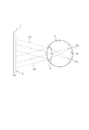
先ず、実施の形態の説明に先立って、本発明に係る画像表示装置の原理について、図1を参照して説明する。 First, prior to the description of the embodiment, the principle of the image display apparatus according to the present invention will be described with reference to FIG.
図1に示すように、観察者が画像表示装置1の観察面2を観察した際、観察面2から眼球3の瞳を通して平行光束L1が入射すると、その光束L1は水晶体4によって網膜5上の位置P1に結像される。また、平行光束L1と異なる角度で観察面2から入射する平行光束L2は、網膜5上の位置P1とは異なる位置P2に結像される。つまり、観察面2から角度の異なる平行光束が眼球3に入射すると、それぞれの平行光束は、網膜5上で異なる位置に結像される。
As shown in FIG. 1, when the observer observes the
本発明に係る画像表示装置の一例では、表示すべき画像の順次の画素の光を、観察面から平行光束としてつまり無限遠からの光として、画素位置に応じてフェーズドアレイにより二次元的に偏向して射出する。これにより、観察者において画像を観察可能とする。 In an example of the image display device according to the present invention, light of sequential pixels of an image to be displayed is two-dimensionally deflected by a phased array as a parallel light beam from the observation surface, that is, as light from infinity according to the pixel position. And inject. Thereby, an observer can observe an image.
以下、本発明の実施の形態について、図を参照して説明する。 Embodiments of the present invention will be described below with reference to the drawings.
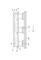
(第1実施の形態)
図2は、第1実施の形態に係る画像表示装置の要部の構成を模式的に示す断面図である。図2に示す画像表示装置100は、光源部200と、観察面として作用する位相シフト部300とを有する。光源部200は、例えば面発光レーザ(VCSEL)201を複数有するVCSELアレイ202を備える。VCSELアレイ202は、例えば特開2005−45243号公報に開示されている公知の構成とすることができ、共通の底部ミラー203及び活性層204と、VCSELごとの頂部ミラー205とを有する。かかる構成のVCSELアレイ202は、底部ミラー203が共通に形成されているので、各VCSEL201から射出されるレーザ光の位相を同期させることができ、コヒーレント光を射出することができる。なお、図2では、図面を明瞭とするために、VCSELアレイ202の構成を省略して示している。
(First embodiment)
FIG. 2 is a cross-sectional view schematically showing a configuration of a main part of the image display device according to the first embodiment. The
VCSELアレイ202は、各VCSEL201のレーザ光が射出されるレーザ射出口206が、x−y軸平面上で例えば図3又は図4に示すように、射出されるレーザ光の波長レベルのピッチで二次元方向に配列されて構成される。図3及び図4は、図2のI−I線からVCSELアレイ202を見た平面図の一部である。図3は、レーザ射出口206が、x軸方向及びy軸方向における配列ピッチの半分のピッチで段違いに配列されている。また、図4は、レーザ射出口206が、x軸方向及びy軸方向に格子状に正方配列されている。なお、図3及び図4では、レーザ射出口206を円形で示しているが、四角形や六角形等の任意の形状とすることができる。また、図2〜図4において、z軸方向は、x及びy軸方向と直交する方向で、各VCSELアレイ201から射出されるレーザ光の方向を示している。これらレーザ射出口の形状及びxyz軸は、他の実施の形態においても同様である。
In the
図2において、位相シフト部300は、VCSELアレイ202のレーザ光の射出側に光学的に結合して配置される。位相シフト部300は、VCSELアレイ202の各VCSEL201に対応する複数の位相シフト素子301を有する。位相シフト素子301は、例えば印加電圧により屈折率が変化するKTN(タンタル酸ニオブ酸カリウム)結晶、LN(ニオブ酸リチウム)結晶、液晶、等の公知の電気光学素子を用いて構成される。以下の説明では、電気光学素子としてKTN結晶302を用いるものとする。
In FIG. 2, the
位相シフト素子301は、VCSEL201からの光の入射側に接合された領域電極部303と、光の射出側に各位相シフト素子301に対して共通に接合された透明な共通電極304とを有している。領域電極部303は、例えば透明な領域電極と、当該領域電極に接続されたスイッチング素子であるTFT(Thin Film Transistor)とを有して構成される。また、領域電極部303側には、各位相シフト素子301を選択するX軸配線305及びY軸配線306が形成される。
The
X軸配線305及びY軸配線306は、後述のX軸配線駆動回路及びY軸配線駆動回路に接続されて、X軸配線駆動回路によりX軸配線305が駆動され、Y軸配線駆動回路によりY軸配線306が駆動される。ここで、X軸配線駆動回路及びY軸配線駆動回路は、各位相シフト素子301をパッシブマトリックス方式により駆動するように構成することもできるが、アクティブマトリックス方式により駆動するように構成するのが好ましい。
The
図2において、位相シフト素子301は、一枚のKTN結晶302に各VCSEL201に対応する領域電極部303を形成することで構成されている。しかし、位相シフト素子301は、図5に示すように、Y軸配線306の単位で分離されたKTN結晶302に領域電極部303を形成して構成してもよい。あるいは、図示しないが、X軸配線単位で分離されたKTN結晶302に領域電極部303を形成して構成してもよい。また、領域電極部303は、例えばスイッチング素子を当該位相シフト素子302の光路外に形成できれば、領域電極のみで構成することができる。この場合、スイッチング素子は、必ずしもTFTとする必要はない。
In FIG. 2, the
ここで、KTN結晶302を有する位相シフト素子301は、図6に示すように、領域電極307と共通電極304との間に電圧Vが印加されると、カー効果によって電圧Vの印加方向(z軸方向)に屈折率分布が生じる。この場合のz軸方向の屈折率変化δn(z)は、下式(1)で表される。ただし、式(1)において、n0は屈折率、ε0は真空の誘電率、εrは比誘電率、dはKTN結晶302のz軸方向の厚さ、zは領域電極307からのz軸方向の距離を示す。
Here, in the

したがって、位相シフト素子301に電圧Vが印加されると、領域電極307と共通電極304との間を透過する光の位相変化Δpは、下式(2)で表される。ただし、式(2)において、λは透過光の波長を示す。
Therefore, when the voltage V is applied to the
次に、図7〜図11を参照して、位相シフト部300が位相シフト素子301をアクティブマトリックス方式により駆動する場合について説明する。なお、以下の説明では、VCSELアレイ202が図4に示した正方配列されている場合を想定している。また、各位相シフト素子301の領域電極部303には、領域電極307とTFT308とが形成されている場合を想定している。図7に示すように、X軸配線305はX軸配線駆動回路310に接続され、Y軸配線306はY軸配線駆動回路311に接続されている。
Next, a case where the
先ず、図7を参照して、VCSELアレイ202の各VCSEL201に対応する位相シフト素子301の駆動回路の構成について説明する。なお、実際の回路では、SN比改善や高速化のための電子部品が付加される場合もあるが、図7は位相シフト素子301の駆動回路の等価回路を示す。KTN結晶302は誘電体として機能するので、キャパシタ「C」として表している。また、領域電極307は符号「E」として示し、反対側の共通電極304は下向きの矢印で表している。
First, the configuration of the drive circuit of the
領域電極Eは、TFT308のドレインDに接続され、TFT308のソースSは対応するY軸配線306、すなわちデータ線に接続されて、Y軸配線駆動回路311により所要の電圧が印加される。TFT308のゲートGは対応するX軸配線305、すなわち走査線に接続されている。なお、KTN結晶Cに印加される電圧を保持するために、領域電極Eと次段のX軸配線305との間に蓄積キャパシタCsが形成されている。なお、図7においては、図面を明瞭とするため、主として一つの位相シフト素子301に対応する部分に符号を示している。
The region electrode E is connected to the drain D of the
図7は、3×3の位相シフト素子(領域電極E)の配列部分を取り出して描いているが、実際にはVCSELアレイは多くのVCSELで構成されており、領域電極EもVCSELの数だけ存在している。そして、Y軸配線駆動回路311からY軸配線306を介して対応するKTN結晶Cの領域電極Eに電圧データに応じた電圧が印加され、X軸配線駆動回路310からX軸配線305を介して対応するTFT308のゲートGに書き込み走査用の制御電圧が印加される。
In FIG. 7, the arrangement portion of the 3 × 3 phase shift elements (region electrodes E) is drawn and drawn, but in reality, the VCSEL array is composed of many VCSELs, and the number of region electrodes E is the same as the number of VCSELs. Existing. A voltage corresponding to the voltage data is applied from the Y-axis
次に、図8を参照して領域電極Eのアクティブマトリックス駆動について説明する。X軸配線駆動回路310により上側のX軸配線305から順番に書き込み制御電圧Vsが加えられる(走査)。現時刻t0では、真ん中のX軸配線305に制御電圧Vsが印加されている。TFT308のゲートGに制御電圧Vsが印加されると、当該X軸配線305に接続されているTFT308は、すべてオンになる。そして、TFT308のドレインDに接続されている領域電極Eに電荷が注入され、各領域電極Eの電位はY軸配線306の電位と同電位になる。これにより、それぞれのVCSEL上の領域電極EにKTN結晶Cに印加する電圧が加わることになる。
Next, active matrix driving of the region electrode E will be described with reference to FIG. The write control voltage Vs is sequentially applied from the upper
つまり、時刻t0における電圧データは、左のY軸配線306から順にV4、V5、V6であり、TFT308がオンになっている中央のX軸配線305に沿った領域電極Eの電位は、それぞれV4、V5、V6となっている。なお、t0より一つ前の制御電圧Vsが上のX軸配線305に加えられた時刻には、Y軸配線306に加えられている電圧はV1、V2、V3であり、対応する領域電極Eに印加されている電圧はV1、V2、V3である。領域電極Eへの印加電圧は、蓄積キャパシタCsによって保持されている。
That is, the voltage data at time t 0 is V 4 , V 5 , V 6 in order from the left Y-
このように、X軸配線305が上から下に順に走査されて、Y軸配線306に送られているKTN印加電圧のデータが各領域電極Eに書き込まれていく。
In this way, the
次に、図9を参照して、位相シフト部300による光束の偏向について説明する。VCSELアレイ202の各VCSEL201からの光は、等位相の平面波で射出されるが、波が進むに従って回折により球面波に近づいていく。この概略球面波で位相シフト部300に入射する。位相シフト部300の各位相シフト素子の領域電極Eに所望の電圧が印加されると、位相シフト部300の各位相シフト素子から射出される光は位相変化を生じた概略球面波となる。位相シフト部300の各位相シフト素子から射出される位相差を有する球面波は、位相シフト素子が波長レベルのピッチで配列されているので、ホイヘンスの原理により包絡面Eを形成する。つまり、VCSELアレイ202から射出された光が一つの波面となる。すなわち、全体として矢印の方向に進む平面波となる。
Next, the light beam deflection by the
ここで、位相シフト素子の配列ピッチをpi、VCSEL201から射出される光の波長をλ、位相シフト素子間の位相差をφ、位相シフト部300からの平面波の出射角をωとすると、
sinω=λφ/πpi ・・・(3)
の関係が成り立つ。
Here, if the arrangement pitch of the phase shift elements is p i , the wavelength of the light emitted from the
sinω = λφ / πp i (3)
The relationship holds.
したがって、図9に示すように、上式(3)に従って位相差φ(例えば、φ1〜φ7)を生じさせれば、VCSELアレイ202からの光束を偏向させることができる。また、与える位相差の大きさを適切に制御すれば、光束の偏向方向を連続的に変化させることができ、いわゆるフェーズドアレイによる光束の走査が可能となる。
Therefore, as shown in FIG. 9, if the phase difference φ (for example, φ1 to φ7) is generated according to the above equation (3), the light beam from the
図10は、図9の位相シフト部300による位相差の制御を観察面側から見た模式図である。図10に示すように、x軸方向の各行の位相シフト素子301には位相差が順次増加又は減少し、y軸方向の各列の位相シフト素子301には同じ位相差を与えれば、x軸方向に光束を偏向することができる。逆に、y軸方向の各列の位相シフト素子301には位相差が順次増加又は減少し、x軸方向の各行の位相シフト素子301には同じ位相差を与えれば、y軸方向に光束を偏向することができる。また、x軸方向及びy軸方向のデータを混合すれば、x軸方向及びy軸方向に同時に偏向することができる。
FIG. 10 is a schematic diagram of the phase difference control by the
したがって、フェーズドアレイにより連続的に偏向を行えば、VCSELアレイ202から射出される光束をラスター状に走査することができる。そのラスター走査に従ってVCSELアレイ202の光強度を変調すれば、画像を表示することができる。あるいは、VCSELアレイ202から観察者までの光路中に光強度変調器を設けて、画像を表示しても良い。これにより、観察者は、位相シフト部300を観察することにより、二次元画像の虚像を観察することができる。
Therefore, if the deflection is continuously performed by the phased array, the light beam emitted from the
また、図11に示すように、包絡面Eが球面波となるように位相差φ1〜φ7を制御することも可能である。この場合、図11に実線で示すように、球の中心が装置の奥側つまり観察者からVCSELアレイ202よりも前方側となる球面波を射出することで、観察者は有限の距離にピントを合わせた場合でも、画像をはっきり見ることができる。また、図11に破線で示すように、球の中心が観察者の後ろ側となる球面波を射出することで、遠視の観察者でも画像を明瞭に観察させることが可能となる。この場合、スクリーンを設置すれば、像を投影することができるので、プロジェクタとしても使用することも可能となる。
Moreover, as shown in FIG. 11, it is also possible to control the phase differences φ1 to φ7 so that the envelope surface E becomes a spherical wave. In this case, as shown by a solid line in FIG. 11, the observer focuses on a finite distance by emitting a spherical wave whose center is on the back side of the apparatus, that is, on the front side of the
以下、具体例について説明する。VCSELアレイ202のVCSEL配列を、図4の正方配列とし、VCSEL間ピッチを1.5μm、観察面の大きさすなわち開口(瞳)の大きさを100mm×50mmとすると、VCSEL数は、66,667×33,333個となる。したがって、図7に示したアクティブマトリックス方式により駆動する場合、X軸配線305は33,333本となり、全領域電極を一回書き換えるのに上から順に33,333回のVs信号を出力すればよいことになる。ここで、図10に示したように、位相シフト部300の全ての位相シフト素子で光束の偏向方向を制御して、SVGA(画素数800×600)の画面をフレームレート30fpsで表示するには、書き換え速度を480,000×30Hz=14.4MHzとし、Y軸配線306への電圧データの送出タイミングは、14.4MHz×33,333=479GHzとすればよい。この場合、Vs信号の幅すなわちTFT308のスイッチング速度は、2psとなる。
Hereinafter, specific examples will be described. If the VCSEL array of the
また、光束の偏向制御は、位相シフト部300の全ての位相シフト素子で行う場合に限らず、位相シフト部300を分割して制御することも可能である。この場合の分割領域は、例えば、回折による広がりが悪影響を与えない0.5mm×0.5mm程度から数mm×数mm程度が好ましい。この場合、異なる区分のVCSELの位相を同期させる必要はなく、各区分間の光束は相互にインコヒーレントである。0.5mm×0.5mmの場合、VCSEL数は、333×333個となる。また、Y軸配線306への電圧データの送出タイミングは、14.4MHz×333=4.8GHzとなり、Vs信号の幅すなわちTFT308のスイッチング速度は、0.2nsとなる。したがって、前者の全ての位相シフト素子で偏向を制御する場合に比べて、X軸配線駆動回路310及びY軸配線駆動回路311の構成が容易になる。
Further, the deflection control of the light beam is not limited to the case where it is performed by all the phase shift elements of the
本実施の形態によると、以下の構成が可能となる。
<VCSELアレイ202が図3に示した配列の場合>
位相シフト素子間=VCSEL間のx軸方向ピッチ:2.4μm
y軸方向ピッチ:1.2μm
KTN結晶の厚みd:1μm
KTN結晶への印加電圧:0〜4.18V(位相差0〜λ)
VCSELアレイの射出光の波長(λ):640nm
走査最大角度(半角):x軸方向18.75度
y軸方向15.5度
観察面の大きさ:100mm×50mm
フレームレート:30fps
X軸配線数=走査線本数:600〜1080本
According to the present embodiment, the following configuration is possible.
<When
Between phase shift elements = pitch in the x-axis direction between VCSELs: 2.4 μm
Y-axis direction pitch: 1.2 μm
KTN crystal thickness d: 1 μm
Applied voltage to KTN crystal: 0 to 4.18 V (
Wavelength (λ) of emission light of the VCSEL array: 640 nm
Maximum scanning angle (half angle): 18.75 degrees in the x-axis direction
Y-axis direction 15.5 degrees Observation surface size: 100 mm x 50 mm
Frame rate: 30 fps
Number of X-axis wirings = Number of scanning lines: 600 to 1080
<VCSELアレイ202が図4に示した配列の場合>
位相シフト素子間=VCSEL間のx軸方向ピッチ:1.5μm
y軸方向ピッチ:1.5μm
KTN結晶の厚みd:1μm
KTN結晶への印加電圧:0〜4.18V(位相差0〜λ)
VCSELアレイの射出光の波長(λ):640nm
走査最大角度(半角):x軸方向25度
y軸方向25度
観察面の大きさ:100mm×50mm
フレームレート:30fps
X軸配線数=走査線本数:600〜1080本
<When
Between phase shift elements = x-axis direction pitch between VCSELs: 1.5 μm
Y-axis direction pitch: 1.5 μm
KTN crystal thickness d: 1 μm
Applied voltage to KTN crystal: 0 to 4.18 V (
Wavelength (λ) of emission light of the VCSEL array: 640 nm
Maximum scanning angle (half angle): 25 degrees in the x-axis direction
Y-axis direction 25 degrees Observation surface size: 100 mm x 50 mm
Frame rate: 30 fps
Number of X-axis wirings = Number of scanning lines: 600 to 1080
(第2実施の形態)
図12は、第2実施の形態に係る画像表示装置の要部の構成を模式的に示す断面図である。図12に示す画像表示装置130は、カラー画像を表示するもので、第1実施の形態の画像表示装置100と光源部の構成が異なるものである。したがって、第1実施の形態と同様の構成要素には、同一参照符号を付して説明を省略する。
(Second Embodiment)
FIG. 12 is a cross-sectional view schematically showing a configuration of a main part of the image display device according to the second embodiment. An
本実施の形態において、光源部230は、例えば、赤色レーザ光(R)を射出するVCSEL231Rを複数有するVCSELアレイ232Rと、緑色レーザ光(G)を射出するVCSEL231Gを複数有するVCSELアレイ232Gと、青色レーザ光(B)を射出するVCSEL231Bを複数有するVCSELアレイ232Bとを備える。VCSELアレイ232R、232G及び232Bは、第1実施の形態で説明したVCSELアレイ202と同様に、それぞれ共通の底部ミラー233及び射出するレーザ光の波長に対応する活性層234と、VCSELごとの頂部ミラー235とを有して構成される。なお、図12では、図面を明瞭とするために、VCSELアレイ232R、232G及び232Bの各々の構成を省略して示している。また、位相シフト部300のX軸配線及びY軸配線の図示を省略している。
In the present embodiment, the
VCSELアレイ232R、232G及び232Bは、各VCSEL231R、231G及び231Bのレーザ射出口236R、236G及び236Bが、x−y軸平面上で例えば図13示すように、波長レベルのピッチで二次元方向に配列されて構成される。なお、図13は、図12のII-II線からVCSELアレイ232R、232G及び232Bを見た平面図の一部である。すなわち、x軸方向の行については、R行、B行、B行、G行の繰り返しパターンとし、y軸方向の列については、B及びGが交互に並ぶ列と、R及びBが交互に並ぶ列との繰り返しパターンとする。また、同色のレーザ射出口のピッチ及び隣接するレーザ射出口のピッチは、例えば、図13に示すように、同色のレーザ射出口についてはx軸方向のピッチが2μm、y軸方向のピッチが2.3μm、隣接するレーザ射出口については、x軸方向のピッチが1μm、y軸方向のピッチが1.15μmとすることができる。
In the
VCSELアレイ232Bは、図14に図13のIII−III線断面を模式的に示すように、レーザ射出口236B側が、第1実施の形態と同様の構成からなる位相シフト部300に光学的に結合される。また、VCSELアレイ232Gは、図15に図13のIV−IV線断面を模式的に示すように、レーザ射出口236G側が導波路237を介して位相シフト部300に光学的に結合される。同様に、VCSELアレイ232Rは、図16に図13のV−V線断面を模式的に示すように、レーザ射出口236R側が導波路238を介して位相シフト部300に光学的に結合される。位相シフト部300は、VCSELアレイ232R、232G及び232Bの各VCSEL231R、231G及び231Bに対応する複数の位相シフト素子301を有している。
The
図13から明らかなように、本実施の形態に係る画像表示装置130は、青色レーザ光を射出するVCSEL231Bの数を多くして、隣接するVCSEL231Bのピッチを小さくしている。その理由は、上式(3)から、波長λが短いと出射角ωが小さくなるため、波長λの短い青色レーザ光を射出するVCSEL231Bについては、数を多くしてピッチを小さくすることにより、所望の出射角ωが得られるようにするためである。また、もちろん、x軸、y軸各方向の画角に応じて、x軸方向とy軸方向のピッチを異なるものとすることができる。
As is apparent from FIG. 13, the
各色のVCSELアレイ232R、232G及び232Bは、表示すべき画素の色情報に応じて、色順次に或いは同時に点灯される。また、位相シフト部300は、第1実施の形態で説明したと同様に、表示すべき画素位置に応じて射出光をフェーズドアレイにより二次元方向に走査する。これにより、観察者は、位相シフト部300を観察することにより、カラー画像を観察することができる。
The
本実施の形態によると、以下の構成が可能となる。
波長:R;640nm、G;530nm、B;450nm
位相シフト素子間=VCSEL間のピッチ:図13の通り
KTN結晶の厚みd:1μm
KTN結晶への印加電圧:0〜4.18V(位相差0〜λ)
走査最大角度(半角):x軸方向15.4度
y軸方向11.3度
観察面の大きさ:200mm×100mm
フレームレート:30fps
X軸配線数=走査線本数:600〜1080本
According to the present embodiment, the following configuration is possible.
Wavelength: R; 640 nm, G; 530 nm, B; 450 nm
Between phase shift elements = Pitch between VCSELs: As shown in FIG. 13 KTN crystal thickness d: 1 μm
Applied voltage to KTN crystal: 0 to 4.18 V (
Maximum scanning angle (half-width): 15.4 degrees in the x-axis direction
11.3 degrees in the y-axis direction Observation surface size: 200 mm x 100 mm
Frame rate: 30 fps
Number of X-axis wirings = Number of scanning lines: 600 to 1080
(第3実施の形態)
図17は、第3実施の形態に係る画像表示装置の要部の構成を模式的に示す断面図である。図17に示す画像表示装置160は、カラー画像を表示するもので、第1実施の形態の画像表示装置100と光源部の構成が異なるものである。したがって、第1実施の形態と同様の構成要素には、同一参照符号を付して説明を省略する。
(Third embodiment)
FIG. 17 is a cross-sectional view schematically showing a configuration of a main part of the image display device according to the third embodiment. An image display device 160 shown in FIG. 17 displays a color image, and is different from the
本実施の形態において、光源部260は、例えば、赤色レーザ光(R)を射出するレーザダイオード261Rと、緑色レーザ光(G)を射出するレーザダイオード261Gと、青色レーザ光(B)を射出するレーザダイオード261Bと、3個のコリメータレンズ262、263、264と、2個のダイクロイックミラー265、266と、ビームエキスパンダ267とを備える。レーザダイオード261Rから射出される赤色レーザ光は、コリメータレンズ262で平行光に変換され、ダイクロイックミラー265及び263を順次透過した後、ビームエキスパンダ267により光束が拡大されて平行光として位相シフト部300に入射される。レーザダイオード261Gから射出される緑色レーザ光は、コリメータレンズ263で平行光に変換され、ダイクロイックミラー265で反射されて赤色レーザ光の光路と同軸に合成された後、ダイクロイックミラー266を透過し、さらにビームエキスパンダ267により光束が拡大されて平行光として位相シフト部300に入射される。レーザダイオード261Bから射出される青色レーザ光は、コリメータレンズ264で平行光に変換され、ダイクロイックミラー266で反射されて赤色レーザ及び緑色レーザ光の光路と同軸に合成された後、ビームエキスパンダ267により光束が拡大されて平行光として位相シフト部300に入射される。
In the present embodiment, the
各色のレーザダイオード261R、261G及び261Bは、表示すべき画素の色情報に応じて、順次に或いは同時に点灯される。また、位相シフト部300は、波長レベルのピッチで二次元方向に配列された複数の位相シフト素子301を有して構成され、第1実施の形態と同様に、表示すべき画素位置に応じて射出光をフェーズドアレイにより二次元方向に走査する。これにより、観察者は、位相シフト部300を観察することにより、カラー画像を観察することができる。
The
なお、本発明は、上記実施の形態にのみ限定されるものではなく、発明の趣旨を逸脱しない範囲で種々の変形または変更が可能である。例えば、カラー画像を表示する場合、光源はRGBの3色に限らず、さらに例えば黄色を加えた4色以上の波長の光を射出するように構成してもよい。また、上記実施の形態では、位相シフトに電気光学結晶による屈折率変化を用いたが、キャリアプラズマ効果による屈折率変化を用いることもできる。 The present invention is not limited to the above-described embodiment, and various modifications or changes can be made without departing from the spirit of the invention. For example, when displaying a color image, the light source is not limited to three colors of RGB, and may be configured to emit light of four or more wavelengths including yellow, for example. In the above embodiment, the refractive index change due to the electro-optic crystal is used for the phase shift. However, the refractive index change due to the carrier plasma effect can also be used.
100、130、160 画像表示装置
200、230、260 光源部
201、231R、231G、231B 面発光レーザ(VCSEL)
202、232R、232G、232B VCSELアレイ
206、236R、236G、236B レーザ射出口
261R、261G、261B レーザダイオード
265、266 ダイクロイックミラー
267 ビームエキスパンダ
300 位相シフト部
301 位相シフト素子
302 KTN結晶
303 領域電極部
304 共通電極
305 X軸配線
306 Y軸配線
308 TFT
310 X軸配線駆動回路
311 Y軸配線駆動回路
100, 130, 160
202, 232R, 232G,
310 X-axis wiring drive circuit 311 Y-axis wiring drive circuit
Claims (6)
二次元方向に配列された複数の位相シフト素子を有し、前記光源部からのコヒーレント光の波面を二次元方向に走査する位相シフト部と、
を備え、
前記光源部は、複数の前記位相シフト素子に対応する複数の面発光レーザを有し、
且つ、複数の前記面発光レーザは、それぞれ波長の異なる光を射出する複数の面発光レーザからなり、波長の短い光を射出する複数の面発光レーザが波長の長い光を射出する複数の面発光レーザよりも短いピッチで配列されている、ことを特徴とする画像表示装置。 A light source that emits coherent light;
A plurality of phase shift elements arranged in a two-dimensional direction, a phase shift unit that scans a wavefront of coherent light from the light source unit in a two-dimensional direction;
Equipped with a,
The light source unit has a plurality of surface emitting lasers corresponding to the plurality of phase shift elements,
The plurality of surface emitting lasers are composed of a plurality of surface emitting lasers that emit light having different wavelengths, and a plurality of surface emitting lasers that emit light having a short wavelength emit light having a long wavelength. They are arranged at a pitch shorter than the laser, the image display device you wherein a.
Priority Applications (3)
| Application Number | Priority Date | Filing Date | Title |
|---|---|---|---|
| JP2013162682A JP6143601B2 (en) | 2013-08-05 | 2013-08-05 | Image display device |
| PCT/JP2014/003681 WO2015019551A1 (en) | 2013-08-05 | 2014-07-10 | Image display device |
| US15/014,431 US9843778B2 (en) | 2013-08-05 | 2016-02-03 | Image display device |
Applications Claiming Priority (1)
| Application Number | Priority Date | Filing Date | Title |
|---|---|---|---|
| JP2013162682A JP6143601B2 (en) | 2013-08-05 | 2013-08-05 | Image display device |
Publications (3)
| Publication Number | Publication Date |
|---|---|
| JP2015031881A JP2015031881A (en) | 2015-02-16 |
| JP2015031881A5 JP2015031881A5 (en) | 2016-09-01 |
| JP6143601B2 true JP6143601B2 (en) | 2017-06-07 |
Family
ID=52460913
Family Applications (1)
| Application Number | Title | Priority Date | Filing Date |
|---|---|---|---|
| JP2013162682A Active JP6143601B2 (en) | 2013-08-05 | 2013-08-05 | Image display device |
Country Status (3)
| Country | Link |
|---|---|
| US (1) | US9843778B2 (en) |
| JP (1) | JP6143601B2 (en) |
| WO (1) | WO2015019551A1 (en) |
Families Citing this family (2)
| Publication number | Priority date | Publication date | Assignee | Title |
|---|---|---|---|---|
| KR102560705B1 (en) | 2015-12-11 | 2023-07-27 | 삼성전자주식회사 | Beam steering apparatus and method of driving beam steering apparatus, and spatial information acqusition apparatus using the same |
| JP7150648B2 (en) | 2019-03-20 | 2022-10-11 | 三菱重工業株式会社 | Ultrasonic flaw detection device, ultrasonic flaw detection method, and ultrasonic flaw detection program |
Family Cites Families (12)
| Publication number | Priority date | Publication date | Assignee | Title |
|---|---|---|---|---|
| US5233673A (en) * | 1991-10-09 | 1993-08-03 | Hughes Aircraft Company | Output steerable optical phased array |
| EP0562742A1 (en) * | 1992-03-25 | 1993-09-29 | Motorola, Inc. | Direct retinal scan display |
| WO1994019765A1 (en) | 1993-02-19 | 1994-09-01 | Norand Corporation | Phased array laser scanner |
| JP3235762B2 (en) * | 1994-12-06 | 2001-12-04 | 日本電信電話株式会社 | 3D display device |
| GB2326263A (en) * | 1997-06-12 | 1998-12-16 | Sharp Kk | Diffractive spatial light modulator and display |
| CN1096004C (en) * | 1997-11-05 | 2002-12-11 | 朱润枢 | Phased array optical equipment and method |
| US6456419B1 (en) * | 2000-09-29 | 2002-09-24 | Innovative Technology Licensing, Llc | Frequency modulated liquid crystal beamsteering device |
| US7397980B2 (en) | 2004-06-14 | 2008-07-08 | Optium Australia Pty Limited | Dual-source optical wavelength processor |
| JP2007011104A (en) * | 2005-07-01 | 2007-01-18 | National Institute Of Information & Communication Technology | Light beam controller and stereoscopic image display apparatus using the same |
| JP5084540B2 (en) * | 2008-02-06 | 2012-11-28 | キヤノン株式会社 | Vertical cavity surface emitting laser |
| US8515217B2 (en) * | 2009-09-02 | 2013-08-20 | Alcatel Lucent | Vertical optically emitting photonic devices with electronic steering capability |
| JP5722657B2 (en) * | 2011-02-17 | 2015-05-27 | 日本電信電話株式会社 | Spatial optical phase modulator |
-
2013
- 2013-08-05 JP JP2013162682A patent/JP6143601B2/en active Active
-
2014
- 2014-07-10 WO PCT/JP2014/003681 patent/WO2015019551A1/en active Application Filing
-
2016
- 2016-02-03 US US15/014,431 patent/US9843778B2/en active Active
Also Published As
| Publication number | Publication date |
|---|---|
| WO2015019551A1 (en) | 2015-02-12 |
| JP2015031881A (en) | 2015-02-16 |
| US20160156885A1 (en) | 2016-06-02 |
| US9843778B2 (en) | 2017-12-12 |
Similar Documents
| Publication | Publication Date | Title |
|---|---|---|
| US10490140B2 (en) | Light deflector and display apparatus | |
| KR101780865B1 (en) | Display device | |
| US8643928B2 (en) | Illumination systems for visual displays | |
| US5802222A (en) | Color image generation systems and applications | |
| JP4930071B2 (en) | Display device | |
| US11144010B2 (en) | Focus modulation optical system and holographic display device having the same | |
| JP6107185B2 (en) | Image forming apparatus and image display apparatus | |
| US10951867B2 (en) | Light emitter architecture for scanning display device | |
| TWI478137B (en) | Display device | |
| JP4850554B2 (en) | 3D display device | |
| JP2008209568A (en) | Electrooptical element and scanning type optical device | |
| JP6728596B2 (en) | Light modulator, optical module, and image display device | |
| JP2008180758A (en) | Display device | |
| CN105467586A (en) | Image display apparatus | |
| JP6549909B2 (en) | Ray control element and stereoscopic display device | |
| JP6143601B2 (en) | Image display device | |
| US20210373321A1 (en) | Display device | |
| JP6305855B2 (en) | Image display device | |
| JP2020077911A (en) | Projector and method for controlling projector | |
| CN110687678B (en) | Display module based on waveguide, image generation module and application thereof | |
| JP3947067B2 (en) | Optical path shift element | |
| KR102595759B1 (en) | Light modulator and holographic display device including the same | |
| US20240134219A1 (en) | Liquid crystal grating and driving method thereof, and three-dimensional display device | |
| JP5417948B2 (en) | Head-mounted display device | |
| IL303770B1 (en) | Image projector with laser scanning over spatial light modulator |
Legal Events
| Date | Code | Title | Description |
|---|---|---|---|
| A521 | Request for written amendment filed |
Free format text: JAPANESE INTERMEDIATE CODE: A523 Effective date: 20160715 |
|
| A621 | Written request for application examination |
Free format text: JAPANESE INTERMEDIATE CODE: A621 Effective date: 20160715 |
|
| TRDD | Decision of grant or rejection written | ||
| A01 | Written decision to grant a patent or to grant a registration (utility model) |
Free format text: JAPANESE INTERMEDIATE CODE: A01 Effective date: 20170425 |
|
| A61 | First payment of annual fees (during grant procedure) |
Free format text: JAPANESE INTERMEDIATE CODE: A61 Effective date: 20170509 |
|
| R151 | Written notification of patent or utility model registration |
Ref document number: 6143601 Country of ref document: JP Free format text: JAPANESE INTERMEDIATE CODE: R151 |
|
| R250 | Receipt of annual fees |
Free format text: JAPANESE INTERMEDIATE CODE: R250 |
|
| R250 | Receipt of annual fees |
Free format text: JAPANESE INTERMEDIATE CODE: R250 |
|
| R250 | Receipt of annual fees |
Free format text: JAPANESE INTERMEDIATE CODE: R250 |
|
| R250 | Receipt of annual fees |
Free format text: JAPANESE INTERMEDIATE CODE: R250 |