JP6139505B2 - Etching system and method for single wafer processing - Google Patents
Etching system and method for single wafer processing Download PDFInfo
- Publication number
- JP6139505B2 JP6139505B2 JP2014502892A JP2014502892A JP6139505B2 JP 6139505 B2 JP6139505 B2 JP 6139505B2 JP 2014502892 A JP2014502892 A JP 2014502892A JP 2014502892 A JP2014502892 A JP 2014502892A JP 6139505 B2 JP6139505 B2 JP 6139505B2
- Authority
- JP
- Japan
- Prior art keywords
- etching
- steam
- substrate
- processing
- mask layer
- Prior art date
- Legal status (The legal status is an assumption and is not a legal conclusion. Google has not performed a legal analysis and makes no representation as to the accuracy of the status listed.)
- Active
Links
Images


Classifications
-
- H—ELECTRICITY
- H01—ELECTRIC ELEMENTS
- H01L—SEMICONDUCTOR DEVICES NOT COVERED BY CLASS H10
- H01L21/00—Processes or apparatus adapted for the manufacture or treatment of semiconductor or solid state devices or of parts thereof
- H01L21/02—Manufacture or treatment of semiconductor devices or of parts thereof
- H01L21/04—Manufacture or treatment of semiconductor devices or of parts thereof the devices having at least one potential-jump barrier or surface barrier, e.g. PN junction, depletion layer or carrier concentration layer
- H01L21/18—Manufacture or treatment of semiconductor devices or of parts thereof the devices having at least one potential-jump barrier or surface barrier, e.g. PN junction, depletion layer or carrier concentration layer the devices having semiconductor bodies comprising elements of Group IV of the Periodic System or AIIIBV compounds with or without impurities, e.g. doping materials
- H01L21/30—Treatment of semiconductor bodies using processes or apparatus not provided for in groups H01L21/20 - H01L21/26
- H01L21/31—Treatment of semiconductor bodies using processes or apparatus not provided for in groups H01L21/20 - H01L21/26 to form insulating layers thereon, e.g. for masking or by using photolithographic techniques; After treatment of these layers; Selection of materials for these layers
- H01L21/3105—After-treatment
- H01L21/311—Etching the insulating layers by chemical or physical means
- H01L21/31105—Etching inorganic layers
- H01L21/31111—Etching inorganic layers by chemical means
-
- H—ELECTRICITY
- H01—ELECTRIC ELEMENTS
- H01L—SEMICONDUCTOR DEVICES NOT COVERED BY CLASS H10
- H01L21/00—Processes or apparatus adapted for the manufacture or treatment of semiconductor or solid state devices or of parts thereof
- H01L21/02—Manufacture or treatment of semiconductor devices or of parts thereof
- H01L21/04—Manufacture or treatment of semiconductor devices or of parts thereof the devices having at least one potential-jump barrier or surface barrier, e.g. PN junction, depletion layer or carrier concentration layer
- H01L21/18—Manufacture or treatment of semiconductor devices or of parts thereof the devices having at least one potential-jump barrier or surface barrier, e.g. PN junction, depletion layer or carrier concentration layer the devices having semiconductor bodies comprising elements of Group IV of the Periodic System or AIIIBV compounds with or without impurities, e.g. doping materials
- H01L21/30—Treatment of semiconductor bodies using processes or apparatus not provided for in groups H01L21/20 - H01L21/26
- H01L21/31—Treatment of semiconductor bodies using processes or apparatus not provided for in groups H01L21/20 - H01L21/26 to form insulating layers thereon, e.g. for masking or by using photolithographic techniques; After treatment of these layers; Selection of materials for these layers
- H01L21/3105—After-treatment
- H01L21/311—Etching the insulating layers by chemical or physical means
-
- H—ELECTRICITY
- H01—ELECTRIC ELEMENTS
- H01L—SEMICONDUCTOR DEVICES NOT COVERED BY CLASS H10
- H01L21/00—Processes or apparatus adapted for the manufacture or treatment of semiconductor or solid state devices or of parts thereof
- H01L21/02—Manufacture or treatment of semiconductor devices or of parts thereof
- H01L21/04—Manufacture or treatment of semiconductor devices or of parts thereof the devices having at least one potential-jump barrier or surface barrier, e.g. PN junction, depletion layer or carrier concentration layer
- H01L21/18—Manufacture or treatment of semiconductor devices or of parts thereof the devices having at least one potential-jump barrier or surface barrier, e.g. PN junction, depletion layer or carrier concentration layer the devices having semiconductor bodies comprising elements of Group IV of the Periodic System or AIIIBV compounds with or without impurities, e.g. doping materials
- H01L21/30—Treatment of semiconductor bodies using processes or apparatus not provided for in groups H01L21/20 - H01L21/26
- H01L21/302—Treatment of semiconductor bodies using processes or apparatus not provided for in groups H01L21/20 - H01L21/26 to change their surface-physical characteristics or shape, e.g. etching, polishing, cutting
- H01L21/306—Chemical or electrical treatment, e.g. electrolytic etching
- H01L21/30604—Chemical etching
- H01L21/30612—Etching of AIIIBV compounds
-
- H—ELECTRICITY
- H01—ELECTRIC ELEMENTS
- H01L—SEMICONDUCTOR DEVICES NOT COVERED BY CLASS H10
- H01L21/00—Processes or apparatus adapted for the manufacture or treatment of semiconductor or solid state devices or of parts thereof
- H01L21/02—Manufacture or treatment of semiconductor devices or of parts thereof
- H01L21/04—Manufacture or treatment of semiconductor devices or of parts thereof the devices having at least one potential-jump barrier or surface barrier, e.g. PN junction, depletion layer or carrier concentration layer
- H01L21/18—Manufacture or treatment of semiconductor devices or of parts thereof the devices having at least one potential-jump barrier or surface barrier, e.g. PN junction, depletion layer or carrier concentration layer the devices having semiconductor bodies comprising elements of Group IV of the Periodic System or AIIIBV compounds with or without impurities, e.g. doping materials
- H01L21/30—Treatment of semiconductor bodies using processes or apparatus not provided for in groups H01L21/20 - H01L21/26
- H01L21/31—Treatment of semiconductor bodies using processes or apparatus not provided for in groups H01L21/20 - H01L21/26 to form insulating layers thereon, e.g. for masking or by using photolithographic techniques; After treatment of these layers; Selection of materials for these layers
- H01L21/3105—After-treatment
- H01L21/311—Etching the insulating layers by chemical or physical means
- H01L21/31144—Etching the insulating layers by chemical or physical means using masks
-
- H—ELECTRICITY
- H01—ELECTRIC ELEMENTS
- H01L—SEMICONDUCTOR DEVICES NOT COVERED BY CLASS H10
- H01L21/00—Processes or apparatus adapted for the manufacture or treatment of semiconductor or solid state devices or of parts thereof
- H01L21/67—Apparatus specially adapted for handling semiconductor or electric solid state devices during manufacture or treatment thereof; Apparatus specially adapted for handling wafers during manufacture or treatment of semiconductor or electric solid state devices or components ; Apparatus not specifically provided for elsewhere
- H01L21/67005—Apparatus not specifically provided for elsewhere
- H01L21/67011—Apparatus for manufacture or treatment
- H01L21/67017—Apparatus for fluid treatment
- H01L21/67063—Apparatus for fluid treatment for etching
- H01L21/67075—Apparatus for fluid treatment for etching for wet etching
- H01L21/67086—Apparatus for fluid treatment for etching for wet etching with the semiconductor substrates being dipped in baths or vessels
-
- B—PERFORMING OPERATIONS; TRANSPORTING
- B08—CLEANING
- B08B—CLEANING IN GENERAL; PREVENTION OF FOULING IN GENERAL
- B08B2203/00—Details of cleaning machines or methods involving the use or presence of liquid or steam
- B08B2203/007—Heating the liquid
-
- B—PERFORMING OPERATIONS; TRANSPORTING
- B08—CLEANING
- B08B—CLEANING IN GENERAL; PREVENTION OF FOULING IN GENERAL
- B08B3/00—Cleaning by methods involving the use or presence of liquid or steam
-
- B—PERFORMING OPERATIONS; TRANSPORTING
- B08—CLEANING
- B08B—CLEANING IN GENERAL; PREVENTION OF FOULING IN GENERAL
- B08B3/00—Cleaning by methods involving the use or presence of liquid or steam
- B08B3/02—Cleaning by the force of jets or sprays
- B08B3/024—Cleaning by means of spray elements moving over the surface to be cleaned
-
- B—PERFORMING OPERATIONS; TRANSPORTING
- B08—CLEANING
- B08B—CLEANING IN GENERAL; PREVENTION OF FOULING IN GENERAL
- B08B3/00—Cleaning by methods involving the use or presence of liquid or steam
- B08B3/04—Cleaning involving contact with liquid
-
- B—PERFORMING OPERATIONS; TRANSPORTING
- B08—CLEANING
- B08B—CLEANING IN GENERAL; PREVENTION OF FOULING IN GENERAL
- B08B3/00—Cleaning by methods involving the use or presence of liquid or steam
- B08B3/04—Cleaning involving contact with liquid
- B08B3/08—Cleaning involving contact with liquid the liquid having chemical or dissolving effect
-
- B—PERFORMING OPERATIONS; TRANSPORTING
- B08—CLEANING
- B08B—CLEANING IN GENERAL; PREVENTION OF FOULING IN GENERAL
- B08B9/00—Cleaning hollow articles by methods or apparatus specially adapted thereto
- B08B9/08—Cleaning containers, e.g. tanks
-
- H—ELECTRICITY
- H01—ELECTRIC ELEMENTS
- H01L—SEMICONDUCTOR DEVICES NOT COVERED BY CLASS H10
- H01L21/00—Processes or apparatus adapted for the manufacture or treatment of semiconductor or solid state devices or of parts thereof
- H01L21/02—Manufacture or treatment of semiconductor devices or of parts thereof
- H01L21/02041—Cleaning
- H01L21/02043—Cleaning before device manufacture, i.e. Begin-Of-Line process
- H01L21/02052—Wet cleaning only
-
- H—ELECTRICITY
- H01—ELECTRIC ELEMENTS
- H01L—SEMICONDUCTOR DEVICES NOT COVERED BY CLASS H10
- H01L21/00—Processes or apparatus adapted for the manufacture or treatment of semiconductor or solid state devices or of parts thereof
- H01L21/02—Manufacture or treatment of semiconductor devices or of parts thereof
- H01L21/02041—Cleaning
- H01L21/02057—Cleaning during device manufacture
-
- H—ELECTRICITY
- H01—ELECTRIC ELEMENTS
- H01L—SEMICONDUCTOR DEVICES NOT COVERED BY CLASS H10
- H01L21/00—Processes or apparatus adapted for the manufacture or treatment of semiconductor or solid state devices or of parts thereof
- H01L21/02—Manufacture or treatment of semiconductor devices or of parts thereof
- H01L21/04—Manufacture or treatment of semiconductor devices or of parts thereof the devices having at least one potential-jump barrier or surface barrier, e.g. PN junction, depletion layer or carrier concentration layer
- H01L21/18—Manufacture or treatment of semiconductor devices or of parts thereof the devices having at least one potential-jump barrier or surface barrier, e.g. PN junction, depletion layer or carrier concentration layer the devices having semiconductor bodies comprising elements of Group IV of the Periodic System or AIIIBV compounds with or without impurities, e.g. doping materials
- H01L21/26—Bombardment with radiation
- H01L21/263—Bombardment with radiation with high-energy radiation
- H01L21/265—Bombardment with radiation with high-energy radiation producing ion implantation
- H01L21/26506—Bombardment with radiation with high-energy radiation producing ion implantation in group IV semiconductors
-
- H—ELECTRICITY
- H01—ELECTRIC ELEMENTS
- H01L—SEMICONDUCTOR DEVICES NOT COVERED BY CLASS H10
- H01L21/00—Processes or apparatus adapted for the manufacture or treatment of semiconductor or solid state devices or of parts thereof
- H01L21/02—Manufacture or treatment of semiconductor devices or of parts thereof
- H01L21/04—Manufacture or treatment of semiconductor devices or of parts thereof the devices having at least one potential-jump barrier or surface barrier, e.g. PN junction, depletion layer or carrier concentration layer
- H01L21/18—Manufacture or treatment of semiconductor devices or of parts thereof the devices having at least one potential-jump barrier or surface barrier, e.g. PN junction, depletion layer or carrier concentration layer the devices having semiconductor bodies comprising elements of Group IV of the Periodic System or AIIIBV compounds with or without impurities, e.g. doping materials
- H01L21/30—Treatment of semiconductor bodies using processes or apparatus not provided for in groups H01L21/20 - H01L21/26
- H01L21/302—Treatment of semiconductor bodies using processes or apparatus not provided for in groups H01L21/20 - H01L21/26 to change their surface-physical characteristics or shape, e.g. etching, polishing, cutting
- H01L21/306—Chemical or electrical treatment, e.g. electrolytic etching
- H01L21/30604—Chemical etching
-
- H—ELECTRICITY
- H01—ELECTRIC ELEMENTS
- H01L—SEMICONDUCTOR DEVICES NOT COVERED BY CLASS H10
- H01L21/00—Processes or apparatus adapted for the manufacture or treatment of semiconductor or solid state devices or of parts thereof
- H01L21/02—Manufacture or treatment of semiconductor devices or of parts thereof
- H01L21/04—Manufacture or treatment of semiconductor devices or of parts thereof the devices having at least one potential-jump barrier or surface barrier, e.g. PN junction, depletion layer or carrier concentration layer
- H01L21/18—Manufacture or treatment of semiconductor devices or of parts thereof the devices having at least one potential-jump barrier or surface barrier, e.g. PN junction, depletion layer or carrier concentration layer the devices having semiconductor bodies comprising elements of Group IV of the Periodic System or AIIIBV compounds with or without impurities, e.g. doping materials
- H01L21/30—Treatment of semiconductor bodies using processes or apparatus not provided for in groups H01L21/20 - H01L21/26
- H01L21/31—Treatment of semiconductor bodies using processes or apparatus not provided for in groups H01L21/20 - H01L21/26 to form insulating layers thereon, e.g. for masking or by using photolithographic techniques; After treatment of these layers; Selection of materials for these layers
- H01L21/3105—After-treatment
- H01L21/311—Etching the insulating layers by chemical or physical means
- H01L21/31127—Etching organic layers
- H01L21/31133—Etching organic layers by chemical means
-
- H—ELECTRICITY
- H01—ELECTRIC ELEMENTS
- H01L—SEMICONDUCTOR DEVICES NOT COVERED BY CLASS H10
- H01L21/00—Processes or apparatus adapted for the manufacture or treatment of semiconductor or solid state devices or of parts thereof
- H01L21/67—Apparatus specially adapted for handling semiconductor or electric solid state devices during manufacture or treatment thereof; Apparatus specially adapted for handling wafers during manufacture or treatment of semiconductor or electric solid state devices or components ; Apparatus not specifically provided for elsewhere
- H01L21/67005—Apparatus not specifically provided for elsewhere
- H01L21/67011—Apparatus for manufacture or treatment
- H01L21/67017—Apparatus for fluid treatment
- H01L21/67028—Apparatus for fluid treatment for cleaning followed by drying, rinsing, stripping, blasting or the like
- H01L21/6704—Apparatus for fluid treatment for cleaning followed by drying, rinsing, stripping, blasting or the like for wet cleaning or washing
- H01L21/67051—Apparatus for fluid treatment for cleaning followed by drying, rinsing, stripping, blasting or the like for wet cleaning or washing using mainly spraying means, e.g. nozzles
-
- H—ELECTRICITY
- H01—ELECTRIC ELEMENTS
- H01L—SEMICONDUCTOR DEVICES NOT COVERED BY CLASS H10
- H01L21/00—Processes or apparatus adapted for the manufacture or treatment of semiconductor or solid state devices or of parts thereof
- H01L21/67—Apparatus specially adapted for handling semiconductor or electric solid state devices during manufacture or treatment thereof; Apparatus specially adapted for handling wafers during manufacture or treatment of semiconductor or electric solid state devices or components ; Apparatus not specifically provided for elsewhere
- H01L21/67005—Apparatus not specifically provided for elsewhere
- H01L21/67011—Apparatus for manufacture or treatment
- H01L21/67017—Apparatus for fluid treatment
- H01L21/67028—Apparatus for fluid treatment for cleaning followed by drying, rinsing, stripping, blasting or the like
- H01L21/6704—Apparatus for fluid treatment for cleaning followed by drying, rinsing, stripping, blasting or the like for wet cleaning or washing
- H01L21/67057—Apparatus for fluid treatment for cleaning followed by drying, rinsing, stripping, blasting or the like for wet cleaning or washing with the semiconductor substrates being dipped in baths or vessels
-
- H—ELECTRICITY
- H01—ELECTRIC ELEMENTS
- H01L—SEMICONDUCTOR DEVICES NOT COVERED BY CLASS H10
- H01L21/00—Processes or apparatus adapted for the manufacture or treatment of semiconductor or solid state devices or of parts thereof
- H01L21/67—Apparatus specially adapted for handling semiconductor or electric solid state devices during manufacture or treatment thereof; Apparatus specially adapted for handling wafers during manufacture or treatment of semiconductor or electric solid state devices or components ; Apparatus not specifically provided for elsewhere
- H01L21/67005—Apparatus not specifically provided for elsewhere
- H01L21/67011—Apparatus for manufacture or treatment
- H01L21/67017—Apparatus for fluid treatment
- H01L21/67063—Apparatus for fluid treatment for etching
- H01L21/67075—Apparatus for fluid treatment for etching for wet etching
- H01L21/6708—Apparatus for fluid treatment for etching for wet etching using mainly spraying means, e.g. nozzles
Description
本願は概して、枚葉式エッチング処理を用いたマスク層のエッチングのエッチング速度と選択性を増大させるエッチング処理システム及び方法の設計に関する。 The present application generally relates to the design of etching systems and methods that increase the etch rate and selectivity of mask layer etching using a single wafer etch process.
相補型金属−酸化物−半導体(CMOS)トランジスタを製造する現在の方法は、活性デバイス領域−たとえば誘電体、金属インターコネクト、歪み、ソース/ドレイン等−を分離及び保護するマスク層を必要とする。シリコン窒化物(Si3N4)又はシリコン酸化物(SiOx)(x>0)は通常マスク層として用いられる。その理由は、Si3N4の電気的特性とモフォロジーが二酸化シリコン(SiO2)と似ており、かつ、シリコン窒化物がSiO2に容易に結合するためである。一般的にはシリコン窒化物は、エッチストップ層として用いられるが、場合によっては(たとえば「デュアルダマシン」プロセスでは)、シリコン窒化物は、慎重に制御された下地の二酸化シリコン層の厚さを変化させることなくエッチングにより除去されなければならない。そのような場合、シリコン窒化物のエッチング速度を二酸化シリコンのエッチング速度によって除することによって計算される、二酸化シリコンに対するシリコン窒化物のエッチング選択性は、プロセスマージンを改善するように可能な限り高いことが理想的である。デバイスは縮小し続けているので、マスク層と下地層の厚さは共に縮小する。超薄膜のエッチング選択性は将来大きな課題になる。 Current methods of fabricating complementary metal-oxide-semiconductor (CMOS) transistors require a mask layer that isolates and protects active device regions, such as dielectrics, metal interconnects, strains, source / drains, and the like. Silicon nitride (Si 3 N 4 ) or silicon oxide (SiO x ) (x> 0) is usually used as a mask layer. This is because the electrical properties and morphology of Si 3 N 4 are similar to silicon dioxide (SiO 2 ), and silicon nitride is easily bonded to SiO 2 . Silicon nitride is typically used as an etch stop layer, but in some cases (eg, in a “dual damascene” process), silicon nitride varies the thickness of the underlying silicon dioxide layer with careful control. It must be removed by etching without. In such cases, the silicon nitride etch selectivity to silicon dioxide, calculated by dividing the silicon nitride etch rate by the silicon dioxide etch rate, should be as high as possible to improve the process margin. Is ideal. As the device continues to shrink, both the mask layer and underlayer thicknesses shrink. Etching selectivity for ultra-thin films will be a major issue in the future.
シリコン窒化物を選択的にエッチングする現在の方法は、様々な化学物質及び方法を用いる。乾式プラズマエッチングも水溶性化学エッチングも、シリコン窒化物の除去に用いられる。水溶性化学物質は、希釈フッ化水素(dHF)、フッ化水素/エチレングリコール、及び、リン酸を含んで良い。様々な化学物質を用いる判断は、シリコン窒化物のエッチング速度と酸化物に対するシリコン窒化物の選択性についての要求によって支配される。水溶性化学物質を用いる方法は、乾式方法と比較してコストが低いため好ましい。リン酸中でのシリコン窒化物のエッチング速度は、温度によって強く影響されることがよく知られている。具体的には、エッチング速度は温度上昇に応じて増大する。ウエットベンチの構成−たとえばリン酸水溶液の槽に基板を浸漬させる構成−では、処理温度は、リン酸水溶液の沸点によって制限される。溶液の沸点は、リン酸水溶液中の水の濃度と周辺圧力の関数である。温度を維持する一の現在の方法は、目標温度(典型的な目標温度の範囲は140℃〜160℃である)での沸騰状態を維持するように、加えられる水の体積と槽に対するヒータ出力のタイミング間隔を調節しながら、この沸騰状態の存在を測定するフィードバックループ制御装置による方法である。リン酸水溶液が水を加えられることなく加熱されるとき、そのリン酸水溶液から水が蒸発することで、そのリン酸水溶液の沸点は上昇する。 Current methods of selectively etching silicon nitride use a variety of chemicals and methods. Both dry plasma etching and water-soluble chemical etching are used to remove silicon nitride. Water-soluble chemicals may include diluted hydrogen fluoride (dHF), hydrogen fluoride / ethylene glycol, and phosphoric acid. The decision to use various chemicals is governed by the requirements for silicon nitride etch rate and silicon nitride selectivity over oxide. A method using a water-soluble chemical substance is preferable because the cost is lower than that of a dry method. It is well known that the etching rate of silicon nitride in phosphoric acid is strongly influenced by temperature. Specifically, the etching rate increases with increasing temperature. In the configuration of a wet bench-for example, a configuration in which a substrate is immersed in a phosphoric acid aqueous solution bath-the processing temperature is limited by the boiling point of the phosphoric acid aqueous solution. The boiling point of the solution is a function of the concentration of water in the aqueous phosphoric acid solution and the ambient pressure. One current method of maintaining the temperature is to add the volume of water added and the heater output to the tank so as to maintain the boiling state at the target temperature (typical target temperature range is 140 ° C to 160 ° C) The feedback loop control device measures the presence of the boiling state while adjusting the timing interval. When the aqueous phosphoric acid solution is heated without adding water, the boiling point of the aqueous phosphoric acid solution rises as water evaporates from the aqueous phosphoric acid solution.
リン酸の温度上昇は、製造のためのシリコン窒化物のエッチング速度増大にとっては好ましく、かつ、低い選択性を犠牲にして製造コストを低下させる。その理由は、現在のリン酸再循環タンクでは、高い沸点を可能にするには、水の濃度を低下させることになるためである。水は、シリコン酸化物又はシリコンに対するシリコン窒化物のエッチング選択性を制御する上で重要である。実験結果は、昇温した状態で非沸騰状態(つまり低含水量)になっても、好ましいエッチング選択性が得られないことを示している。反対に、選択性を改善させるためには、水の濃度を高める(つまり酸をさらに希釈する)ことが好ましいが、これは現実的ではない。槽中での水の濃度を増大させることで、酸の混合物の沸点は減少する。低温では、シリコン窒化物のエッチング速度は、シリコン窒化物のエッチング速度と温度との間で強いアレニウス関係が存在するため、顕著に減少する。 An increase in the temperature of phosphoric acid is preferable for increasing the etching rate of silicon nitride for manufacturing and lowers the manufacturing cost at the expense of low selectivity. The reason is that the current phosphoric acid recirculation tank will reduce the concentration of water to allow a high boiling point. Water is important in controlling the etch selectivity of silicon nitride to silicon oxide or silicon. The experimental results show that preferable etching selectivity cannot be obtained even when the temperature rises and the temperature becomes a non-boiling state (that is, low water content). Conversely, to improve selectivity, it is preferable to increase the concentration of water (ie, further dilute the acid), but this is not practical. By increasing the concentration of water in the bath, the boiling point of the acid mixture decreases. At low temperatures, the silicon nitride etch rate is significantly reduced due to the strong Arrhenius relationship between the silicon nitride etch rate and temperature.
現在の技術においては、たとえば特許文献1は、シリコン窒化物絶縁層をマスクする際に用いられるシリコン酸化層のエッチング速度を、沸騰するリン酸水溶液内で制御する方法を開示している。その方法は、沸騰するリン酸水溶液にシリケート材料を意図的に加える。それに加えて特許文献2は、低固相はんだフラックスの組成を連続的に監視及び制御する方法を開示している。そのフラックスの組成物の比重と略一致する比重を有する溶媒をマスク層の高いエッチング速度を維持し、かつ、シリコン又はシリコン酸化物全体に対するマスク層の高いエッチング選択性をも維持する方法及びシステムが、当技術分野において望まれている。エッチング速度、エッチング選択性、エッチング時間、及び/又はコストの目標を満たすことの可能な、バッチエッチング処理システム及び枚葉式基板システム並びに方法が必要とされている。
In the current technology, for example,
基板上のマスク層のエッチング速度と選択性を増大させる方法及びシステムが供される。当該システムは、前記マスク層とシリコン又はシリコン酸化物の層を含む複数の基板、前記マスク層をエッチングするための処理液体を含んで前記複数の基板を処理するエッチング処理チャンバ、及び、前記エッチング処理チャンバと結合して昇圧してスチーム・水蒸気混合物を供給する沸騰装置を有する。前記スチーム・水蒸気混合物は、選択されたエッチング速度と、前記マスク層とシリコン又はシリコン酸化物とのエッチング選択比の目標値を維持するように、制御された速度で前記エッチング処理チャンバへ導入される。 Methods and systems are provided for increasing the etch rate and selectivity of a mask layer on a substrate. The system includes a plurality of substrates including the mask layer and a layer of silicon or silicon oxide, an etching processing chamber for processing the plurality of substrates including a processing liquid for etching the mask layer, and the etching process A boiling device is connected to the chamber and pressurized to supply a steam / water vapor mixture. The steam / water vapor mixture is introduced into the etch process chamber at a controlled rate to maintain a selected etch rate and a target etch selectivity ratio between the mask layer and silicon or silicon oxide. .
図1を参照すると、概略図10が、従来技術に係るバッチエッチング処理システムでのシリコン窒化物のエッチング方法を表している。前記バッチエッチング処理システムでは、エッチング用化学物質(エッチャント)が、1種類以上の入力ストリーム34と38を用いることによって、複数の基板26が設けられるエッチング処理チャンバ44へ供給される。エッチャントは、オーバーフロータンク42とオーバーフロー噴出口18を用いることによって、再利用、リサイクル、又は供給されて良い。ヒータ22はたとえば、プロセスチャンバ44の側部又は底部にヒータを備えることによって与えられても良い。ヒータ22は外付けであっても良いし、又は内蔵されても良い。
Referring to FIG. 1, a schematic diagram 10 illustrates a silicon nitride etching method in a batch etching processing system according to the prior art. In the batch etching system, an etching chemical (etchant) is supplied to an
図2は、エッチング処理チャンバ66とスピルタンク58を有する、シリコン窒化物をエッチングするための従来技術に係るバッチエッチング処理システム50を表す概略図である。上述したように、ヒータ70は、エッチング処理チャンバ66の前方、後方、及び下方に供されて良く、これらのヒータ70は外付けであっても良いし、又は内蔵されても良く、かつ、これらのヒータ70は、処理チャンバ66内の水溶液94へ流入する熱流束46を供して良い。流出する熱流束は、通水62と水90の蒸発を含む。流入する熱流束が、蒸発と通水により流出する熱流束よりも大きい場合、水溶液の温度は、沸騰するまで上昇する。沸点は、酸の濃度と周辺圧力によって調節される。沸騰中、熱が増大することで、水はさらに沸騰されて急速に流出する。水溶液94の沸点を一定に維持するため、処理チャンバ制御装置(図示されていない)は、ヒータ70と、供給ライン78を介して注入される供給水74を同時に制御しなければならない。流入する供給水が、蒸発により失われる水よりも多い場合、水溶液の温度は減少する。その結果酸が希釈されて、沸点が低下する。反対に、流入する供給水が、蒸発により失われる水よりも少ない場合、水溶液の温度は上昇する。その結果酸が濃縮されて、沸点が上昇する。
FIG. 2 is a schematic diagram illustrating a prior art batch
リン酸中でのシリコン窒化物のエッチング速度は、温度による影響を強く受けることがよく知られている。具体的には、エッチング速度は温度上昇に応じて増大する。シリコン窒化物と二酸化シリコンのエッチングの化学反応は以下である。 It is well known that the etching rate of silicon nitride in phosphoric acid is strongly influenced by temperature. Specifically, the etching rate increases with increasing temperature. The chemical reaction of the etching of silicon nitride and silicon dioxide is as follows.

ラウールの法則は、理想溶液の蒸気圧が、各化学成分の蒸気圧と、その溶液中に存在する成分のモル分率に依存するという法則である。一旦溶液中での成分が平衡に到達すると、その溶液の全蒸気圧pは、
p=p*AxA+p*BxB+・・・
で表される。各成文の個々の蒸気圧は、
pi=p*ixi
で表される。ここで、piは混合物中での成分iの分圧で、p*iは純粋な成分iの蒸気圧で、xiは溶液(混合物)中での成分iのモル分率である。
Raoul's law is that the vapor pressure of an ideal solution depends on the vapor pressure of each chemical component and the mole fraction of components present in the solution. Once the components in the solution reach equilibrium, the total vapor pressure p of the solution is
p = p * A x A + p * B x B + ...
It is represented by The individual vapor pressure of each sentence is
p i = p * i x i
It is represented by Where p i is the partial pressure of component i in the mixture, p * i is the vapor pressure of pure component i, and x i is the molar fraction of component i in the solution (mixture).
リン酸と水の平衡状態の例が図5Aに与えられている。温度を維持する現在のTEL EXPEDIUS法は、目標温度(160℃)での沸騰状態を維持するように、加えられる水の体積と槽に対するヒータ出力のタイミング間隔を調節しながら、この沸騰状態の存在を測定するフィードバックループ制御装置による方法である。リン酸水溶液が水を加えられることなく加熱されるとき、そのリン酸水溶液から水が蒸発することで、そのリン酸水溶液の沸点は上昇する。 An example of the equilibrium state of phosphoric acid and water is given in FIG. 5A. The current TEL EXPEDIUS method of maintaining temperature is the presence of this boiling state, adjusting the volume of water added and the heater output timing interval to the bath to maintain the boiling state at the target temperature (160 ° C). It is a method by the feedback loop control apparatus which measures this. When the aqueous phosphoric acid solution is heated without adding water, the boiling point of the aqueous phosphoric acid solution rises as water evaporates from the aqueous phosphoric acid solution.
リン酸の温度上昇は、製造のためのシリコン窒化物のエッチング速度増大にとっては好ましく、かつ、低い選択性を犠牲にして製造コストを低下させる。その理由は、現在のリン酸再循環タンクでは、高い沸点を可能にするには、水の濃度を低下させることになるためである。水は、SiO2に対するシリコン窒化物のエッチング選択性を制御する上で重要である(化学式1,2を参照のこと)。実験結果は、昇温した状態で非沸騰状態(つまり低含水量)になっても、図5Bのように好ましいエッチング選択性が得られないことを示している。反対に、選択性を改善させるためには、水の濃度を高める(つまり酸をさらに希釈する)ことが好ましいが、これは現実的ではない。槽中での水の濃度を増大させることで、酸の混合物の沸点は減少する。低温では、シリコン窒化物のエッチング速度は、シリコン窒化物のエッチング速度と温度との間で強いアレニウス関係が存在するため、顕著に減少する。
An increase in the temperature of phosphoric acid is preferable for increasing the etching rate of silicon nitride for manufacturing and lowers the manufacturing cost at the expense of low selectivity. The reason is that the current phosphoric acid recirculation tank will reduce the concentration of water to allow a high boiling point. Water is important in controlling the etch selectivity of silicon nitride to SiO 2 (see
処理液体という語句は、使用される溶媒が水又は他の溶媒であって良いことを強調するため、明細書の以降の箇所で用いられる。本発明の焦点は、シリコン窒化物への処理液体の供給温度を増大させることでシリコン窒化物のエッチング速度を増大させながら、シリコン又は二酸化シリコンに対するシリコン窒化物の最適エッチング選択性を維持する新規な方法である。高温は、静止又は回転した1枚の基板に供給される前に、リン酸流へ加圧スチームを注入することによって実現される。スチームが凝集することで、潜熱がリン酸へ向かうように解放される。その結果リン酸の加熱が効率的に行われる。他の利点は、リン酸は自動的に常に水によって飽和されることである。水は、二酸化シリコンに対するシリコン窒化物の高いエッチング選択性を維持するのに必要である。1回通過処理では、選択性の制御を容易にするために溶融シリカがリン酸に供給されることが必要である。循環処理では、シリカは、自然のリン酸中に供給されて良いし、又は、エッチング処理システムを介したシリコン窒化物基板全面で循環されて良い(これは、リン酸槽としても知られるバッチエッチング処理システムにおいて用いられる一般的な処理である)。本発明の実施例では、スチーム噴流が、基板上の中心から端部までのエッチング均一性を保証するように、基板を予熱するのに利用されても良い。 The phrase processing liquid will be used later in the specification to emphasize that the solvent used may be water or other solvents. The focus of the present invention is a novel that maintains the optimum etch selectivity of silicon nitride to silicon or silicon dioxide while increasing the etch rate of silicon nitride by increasing the supply temperature of the treatment liquid to the silicon nitride. Is the method. The high temperature is achieved by injecting pressurized steam into the phosphoric acid stream before being fed to a stationary or rotating single substrate. Aggregating steam releases latent heat toward phosphoric acid. As a result, the phosphoric acid is efficiently heated. Another advantage is that phosphoric acid is always automatically saturated with water. Water is necessary to maintain the high etch selectivity of silicon nitride to silicon dioxide. The single pass process requires that fused silica be supplied to phosphoric acid to facilitate selectivity control. In the circulation process, the silica can be supplied in natural phosphoric acid or it can be circulated across the silicon nitride substrate via an etching treatment system (this is a batch etching also known as a phosphoric acid bath). This is a general process used in a processing system). In embodiments of the present invention, a steam jet may be used to preheat the substrate so as to ensure etch uniformity from center to edge on the substrate.
本発明によって解決される問題はとりわけ、枚葉式基板処理を実用的かつ費用対効果良くできるように、処理液体−たとえばリン酸−を用いるシリコン窒化物エッチング速度の処理を改善することである。リン酸処理は一般的には、「汚れた処理」とみなされ、残った粒子を除去する標準洗浄1(SC1)工程が続いて行われる。枚葉式エッチング処理は本質的に、バッチエッチング処理よりも清浄である。その理由は、欠陥の機構/粒子の再堆積及び/又は前面から背面への汚染が回避されうるからである。シリコン窒化物エッチング処理は、160℃の熱いリン酸中では遅い(30〜60Å/min)。シリコン窒化物のエッチング速度が180Å/minを超えるまで増大しうる場合、枚葉式基板処理装置でのシリコン窒化物処理が実用的となる。シリコン窒化物を加熱するのに直接スチーム注入を使用することによって、シリコン又はシリコン窒化物に対するシリコン窒化物のエッチング選択性を高くするのに必要とされる飽和水の量を維持しながら、高い処理温度を実現することができる。 The problem solved by the present invention is, among other things, to improve silicon nitride etch rate processing using processing liquids, such as phosphoric acid, so that single wafer processing can be practical and cost effective. The phosphoric acid treatment is generally considered a “dirty treatment” followed by a standard wash 1 (SC1) step that removes the remaining particles. The single wafer etch process is inherently cleaner than the batch etch process. The reason is that defect mechanisms / particle redeposition and / or front-to-back contamination can be avoided. The silicon nitride etching process is slow (30-60 liters / min) in hot phosphoric acid at 160 ° C. In the case where the silicon nitride etching rate can be increased to exceed 180 Å / min, silicon nitride processing in a single wafer processing apparatus becomes practical. High processing while maintaining the amount of saturated water required to increase silicon nitride etch selectivity to silicon or silicon nitride by using direct steam injection to heat silicon nitride Temperature can be realized.
一の実施例では、沸騰装置(周辺温度では液体の水を供給する)が、昇圧下でスチーム・水蒸気混合物を供給するのに用いられる。スチーム・水蒸気混合物の温度は、ボイラー内部の圧力によって制御されて良い。続いてスチーム・水蒸気混合物は、熱いリン酸から枚葉式基板処理チャンバへの化学物質供給ラインへ注入される。スチーム・水蒸気混合物は、槽への熱と湿気の供給源を与える。よってその槽は標準状態の沸点よりも高温となり、気相と液相の両方に過剰な水蒸気が導入されることで、二酸化シリコン及びシリコンに対する窒化物のエッチング選択性が維持される。 In one embodiment, a boiling device (providing liquid water at ambient temperature) is used to deliver the steam / steam mixture at elevated pressure . The temperature of the steam / steam mixture may be controlled by the pressure inside the boiler. The steam / water vapor mixture is then injected from the hot phosphoric acid into the chemical supply line to the single wafer substrate processing chamber. The steam / steam mixture provides a source of heat and moisture to the vessel. Therefore, the temperature of the bath becomes higher than the boiling point of the standard state, and excess water vapor is introduced into both the gas phase and the liquid phase, so that the etching selectivity of nitride to silicon dioxide and silicon is maintained.
他の実施例では、スチーム・水蒸気混合物は、エッチング処理チャンバへ流入する前に、昇圧して処理液体と混合される。供給ライン中での沸騰を回避するため十分な圧力が維持されなければならない。続いて処理液体は、周辺圧力でエッチング処理チャンバへ流入する際に、急激な沸騰を開始する。他の実施例では、複数のノズルが基板の上方で用いられて良い。第1ノズルは加熱されたリン酸を導入する。第2ノズル又は他のノズルは、リン酸への導入前に基板表面を予熱するために高温のスチーム・水蒸気混合物を導入する。それにより、基板全体にわたる均一な温度が維持され、ひいてはエッチング均一性が保証され易くなる。この実施例では、ノズルの位置とノズルの数は、基板への熱と処理液体の供給効率を最大化するように設定されて良い。スチーム・水蒸気混合物はまた、温度均一性を維持するように基板背面に注入されても良い。 In another embodiment, the steam / water vapor mixture is pressurized and mixed with the process liquid prior to entering the etch process chamber. Sufficient pressure must be maintained to avoid boiling in the supply line. Subsequently, the processing liquid begins to boil rapidly as it flows into the etching processing chamber at ambient pressure. In other embodiments, multiple nozzles may be used above the substrate. The first nozzle introduces heated phosphoric acid. The second nozzle or other nozzle introduces a hot steam / water vapor mixture to preheat the substrate surface prior to introduction into the phosphoric acid. As a result, a uniform temperature is maintained throughout the substrate, and as a result, etching uniformity is easily ensured. In this embodiment, the position of the nozzles and the number of nozzles may be set so as to maximize the efficiency of supplying heat and processing liquid to the substrate. A steam / water vapor mixture may also be injected into the backside of the substrate to maintain temperature uniformity.
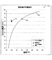
図3は、一の周辺圧力でのリン酸濃度と温度の関数としてリン酸の沸点典型的なグラフ300を表している。処理液体の温度と濃度は、エッチング速度と、シリコン又はシリコン酸化物に対するシリコン窒化物のエッチング選択性を決定する2つの重要な因子である。図3は、リン酸濃度に対するシリコン窒化物のバッチエッチング処理温度の沸騰曲線304を表している。沸騰曲線304を参照して、たとえば処理液体が条件Aの初期設定をとるとすると、処理液体は、約120℃の温度で85質量%のリン酸濃度を有する。処理液体は、沸点が点X(308の参照番号が付されている)によって表されている点に到達するまで加熱される。点Xは、典型的なエッチング処理システムの制御限界をも表す沸騰曲線304中の一点である。上述したように、処理液体の温度は、エッチング速度を増大させるために昇温される。同時にシリコン窒化物のエッチング選択性が維持され、かつ、エッチング均一性が維持される。
FIG. 3 depicts a
図4Aは、一の周辺圧力でのリン酸の濃度の関数としてのリン酸の沸騰曲線404(左側縦軸に表されている)と、エッチング処理システム内での混合物の平衡条件の温度の関数としての蒸気圧曲線408(右側縦軸に表されている)を有する典型的なグラフ400である。リン酸濃度は、水溶液中での質量%として表されている。太い点で表される点(1)での処理液体の初期条件の組は、85%のリン酸組成と120℃の温度に対応するものとする。処理液体は、加熱され、かつ、沸騰曲線404の点線部分によって表される沸点に到達する。加熱は、内蔵又は外付けのヒータを利用してよく、かつ、エッチング処理液体へのスチーム・水蒸気混合物の注入によって実行されて良い。一の実施例では、エッチング処理システムは、沸騰曲線404上の点(2)で表される限界高温を有する。ここで、この限界温度に対応する温度は160℃である。スチームと水蒸気が一緒になったもの(スチーム・水蒸気混合物)は、処理液体が点(3)に到達するまで、エッチング処理システムの底部へ注入される。点(3)は、92質量%のリン酸組成、180℃の温度、及び、約1.0MPaでの蒸気圧に実質的に対応する。スチーム・水蒸気混合物と水溶性リン酸との他の組み合わせが、ある用途の目的を満たすシリコン窒化物のエッチング速度とエッチング選択性を決定するために試されて良い。スチーム・水蒸気混合物の圧力は、0.2〜2.0MPaの範囲であって良い。
FIG. 4A shows a function of the boiling
図4Bを参照して、0.5MPaの圧力が、スチーム・水蒸気混合物の目標圧力として選ばれるものとする。(蒸気圧曲線408上の点Aでの)混合物の対応温度は約152℃である。スチーム・水蒸気混合物が、槽又は枚葉式基板エッチング処理システム中の処理液体へ注入されることで、沸点は、点Aと沸騰曲線404の点A’とを接続する垂直線によって決定される。その結果、平衡状態に対応するリン酸濃度は約86%となる。選ばれた目標圧力が2.0MPaである場合、混合物の対応温度(蒸気圧曲線408上の点B)は約214℃である。同一の方法を用いることによって、沸点は、点Bと沸騰曲線404の点B’とを接続する垂直線によって決定される。その結果、平衡状態に対応するリン酸濃度は約96%となる。よってスチーム・水蒸気混合物の流速と圧力は、処理液体の温度を制御する変数として用いられて良い。スチーム・水蒸気混合物の流速と圧力は、処理液体の沸点、ひいては処理液体中でのリン酸濃度に影響を及ぼす。処理液体の平衡状態のリン酸濃度と温度は、エッチング速度とエッチング選択性に影響を及ぼす。
Referring to FIG. 4B, a pressure of 0.5 MPa shall be chosen as the target pressure for the steam / steam mixture. The corresponding temperature of the mixture (at point A on the vapor pressure curve 408) is about 152 ° C. As the steam / water vapor mixture is injected into the processing liquid in the bath or single wafer substrate etching processing system, the boiling point is determined by the vertical line connecting point A and point A ′ of the boiling
図5Aは、温度(℃)の関数として、立方メートル当たりの水溶性分子のモル数(Aq. mols/m3)として表されるリン酸溶液の組成の第1曲線504と、mols/m3として表される水の第2曲線508を有する典型的なグラフ500を表す。処理液体が160℃〜220℃まで加熱される際、リン酸の濃度は基本的に平坦である。他方水の濃度は、温度の上昇に伴って蒸発により低下する。処理液体のエッチング選択性の変化をさらに示すため、図5Bは、エッチング処理システム内での時間と処理液体の温度の関数としてのリン酸溶液のエッチング選択性の典型的なグラフ500を表している。試験開始時、処理液体(水溶性リン酸)が沸騰し、蒸留水(DIW)が、処理液体を加えるのに用いられ、かつ、二酸化シリコンに対するシリコン窒化物のエッチング選択性554は高い。50分後、DIWを加えるのが中止され、処理液体の温度が約220℃で最高となった。この温度は、ヒータ電力が減少した後に低下する前の温度と略同一である。エッチング選択性曲線564の下方へ向かう傾斜から明らかなように、エッチング選択性も554から558と低下した。DIWを処理液体へ追加するのを中断した後、処理気体は沸騰状態となり、エッチング選択性は558から562へ増大した。本願発明者等は、処理液体が、160〜200℃の範囲で有利で、水溶性リン酸を用いた処理液体にとっては約180℃が好ましいことを発見した。
FIG. 5A shows a
図6Aは、本発明の実施例によるバッチエッチング処理システムの典型的な概略図を表している。複数の基板632がエッチング処理チャンバ640内に設けられている。処理液体628がエッチング処理チャンバ640へ導入される。過剰な処理液体は、オーバーフローコンテナ604へ行き、放出口608を介して廃棄されて良い。スチーム発生装置614には、供給ライン620を介して入力液体が供給される。スチーム発生装置614は、スチーム・水蒸気混合物612を生成するヒータ616によって加熱される。スチーム・水蒸気混合物612は、エッチング処理チャンバ640の底部との接続ライン636によって供給される。制御装置(図示されていない)を用いることで、バッチエッチング処理システム600は、処理液体628及びスチーム・水蒸気混合物612の流速を制御することによって、選択されたエッチング処理速度及び選択されたエッチング選択比を満たすように構成される。処理液体628及びスチーム・水蒸気混合物612は、高圧に加圧されても良いし、されなくても良い。スチーム・水蒸気混合物の圧力は0.2〜2.0MPaの範囲内であって良い。
FIG. 6A represents an exemplary schematic diagram of a batch etching processing system according to an embodiment of the present invention. A plurality of
図6Bは、本発明の実施例による枚葉式基板エッチング処理システムの典型的な概略図を表している。1枚の基板654がステージ662上に載置されている。ステージ662は、基板654を静止させたままにするか、又は、基板654を回転させるように構成される。その一方で、処理液体678が供給ライン682から供給され、かつ、スチーム・水蒸気混合物674が供給ライン670から供給される。スチーム・水蒸気混合物674は、基板654全体にわたって均一な処理を実行するように配置されるノズル666によって、基板654全体にわたって供給ライン670を介して供給される。枚葉式基板処理システム650と相似する多重エッチング処理システムの設定は、複数の配置−たとえば積層、直交、環状、及び、共通の基板搬送システムにより供給可能な他の配置−をとるように構成されて良い。スチームは、余熱すなわち基板654全体にわたって均一な温度を維持するため、スチーム供給ライン658によって基板背面へ供給されて良い。
FIG. 6B represents an exemplary schematic diagram of a single wafer substrate etching system according to an embodiment of the present invention. One substrate 654 is placed on the
図7Aは、本発明の実施例によるノズルを用いてスチーム・水蒸気混合物を供給するバッチエッチング処理システムの典型的な概略図を表している。処理液体738は、エッチング処理チャンバ742の前方と後方に設けられたヒータ716によって加熱されて良い。ヒータ716は外付けであっても良いし、又は内蔵されても良い。ヒータ716は、エッチング処理チャンバ742内の処理液体738に流入する熱流束720を供する。さらに追加の流入する熱流束722が、供給ライン726を介して供給されるスチーム・水蒸気混合物736を処理液体738へ注入することによって供される。流出する熱流束は通水708と水の蒸発734を有する。流入する熱流束が、蒸発による流出する熱流束708と通水による熱流束734よりも大きい場合、処理液体738の温度は沸騰するまで上昇する。沸点は、処理液体738の濃度と周辺圧力によって調節される。沸騰中、熱が増大することで、水はさらに沸騰されて急速に飛び出す。
FIG. 7A represents an exemplary schematic diagram of a batch etching processing system for supplying a steam / water vapor mixture using a nozzle according to an embodiment of the present invention. The
処理液体738の沸騰温度を一定に維持するため、処理チャンバ制御装置(図示されていない)は、ヒータとノズル730を介するスチーム・水蒸気混合物の注入を同時に制御しなければならない。スチーム・水蒸気混合物の供給が、蒸発による水の損失よりも大きい場合、処理液体738の温度は減少する。その結果、処理液体738は希釈され、沸点は低下する。逆に、水の供給が、蒸発による水の損失よりも少ない場合、処理液体738の温度は上昇する。その結果、酸は濃縮され、沸点は上昇する。エッチング処理チャンバ742の底部にノズル730を設けることで、処理液体738内で均一な温度プロファイルを生成するような混合作用が生じる。処理液体738は、第2供給ライン724を介してノズル730へ導入されて良い。余剰の処理液体738はスピルタンク704へ向かう。バッチエッチング処理システム700は、処理液体738の温度を上昇させることによって、マスク層−たとえばシリコン窒化物−のエッチング速度を増大させる方法を供する。シリコン酸化物又はシリコンに対するシリコン窒化物の目標となるエッチング選択性すなわち比もまた、処理液体738のモル濃度を制御する−たとえばスチーム・水蒸気混合物の追加及び/又はノズル730を介して分配されるスチーム・水蒸気混合物の温度の変化−ことによって維持される。
In order to keep the boiling temperature of the
図7Bは、本発明の実施例による処理液体循環システムを有する枚葉式エッチング処理システムの典型的な概略図を表している。処理液体774を循環させることで、化学物質の使用が減少し、かつ、後述するように、左への反応2の平衡を維持するように処理液体中のシリカを高濃度に維持することによって、エッチング選択性が向上する。枚葉式基板エッチング処理システム760を参照すると、1枚の基板796はステージ788上に設けられる。ステージ788は、基板796をエッチング処理チャンバ762内部で静止又は回転させるように構成される。スチーム・水蒸気混合物766は、供給ライン764を用いて供給され、ノズル790を用いることによって基板上に供給される。スチーム796は、スチーム入力ライン768を用いることによって基板796の背面へ供給されることで、基板796の温度は均一に維持される。スチーム769は、スチーム・水蒸気混合物766と同一であって良い。処理液体循環システム783は、エッチング処理チャンバ762の底部と結合する排出ライン786を有する。排出ライン786は、制御バルブ782を通り抜ける。制御バルブ782は、廃棄ライン780を介して処理液体774の一部を廃棄し、かつ、再循環ライン784を介して処理液体774の残りを再循環させる。新たな処理液体774が、処理液体供給ライン776を用いることによって再循環ライン784に導入される。
FIG. 7B depicts an exemplary schematic diagram of a single wafer etch processing system having a processing liquid circulation system according to an embodiment of the present invention. By circulating the
図7Bを参照すると、溶融シリカは、反応2を抑制することによって目標のシリコン窒化物エッチング速度を維持するのを容易にする。一の実施例では、溶融シリカ(Si(OH)4)は、シリカ注入ライン772と供給ライン776を用いることによって注入される。シリカの量は、ある目標の範囲−たとえば10〜30ppmの溶融シリカ−での溶融シリカの量を維持するのに十分なものである。他の実施例では、シリコン窒化物を含む多数の基板796が、再循環する処理液体774中で所望の量の溶融シリカを維持するために処理される。枚葉式基板処理システムを用いる本発明の一の利点は、処理液体中での高濃度のシリカに対する許容度である。リン酸を用いる従来技術に係るバッチエッチング処理システムでは一般的に、シリカの濃度が上昇することで欠陥率が増大する。シリコン酸化物に対するマスク層の安定した選択比の維持を容易にする高濃度シリカの許容度に加えて、枚葉式基板処理システムは、同一ようとであればバッチエッチング処理システムよりも欠陥率が低いので、本質的に有利である。
Referring to FIG. 7B, fused silica facilitates maintaining a target silicon nitride etch rate by inhibiting
図8A、図8B、及び図8Cは、本発明の実施例におけるエッチング処理システム用の搬送システムの概略図である。一の実施例によると、図8Aは、(複数の)基板上で非プラズマ洗浄処理を実行する処理システム800を表している。処理システム800は、第1処理システム816及び該第1処理システム816と結合する第2処理システム812を有する。たとえば、第1処理システム816は、化学処理システム(又は1つの処理チャンバの化学処理部分)を有して良く、かつ、第2処理システム812は、熱処理システム(又は1つの処理チャンバの熱処理部分)を有して良い。
8A, 8B, and 8C are schematic views of a transfer system for an etching processing system in an embodiment of the present invention. According to one embodiment, FIG. 8A depicts a
また図8Aに図示されているように、搬送システム808は、第1処理システム816と第2処理システム812に対して(複数の)基板を搬入出し、かつ、多数の構成要素を備える製造システム804と基板を交換するため、第1処理システム816に結合されて良い。第1処理システム816、第2処理システム812、及び搬送システム808はたとえば、多数の構成要素を備える製造システム804内部に処理用構成要素を有して良い。たとえば多数の構成要素を備える製造システム804は、処理用構成要素−たとえばエッチング処理システム、堆積システム、コーティングシステム、パターニングシステム、計測システム等を含む−に対して(複数の)基板を搬入出することを可能にする。第1システム内で起こる処理と第2システム内で起こる処理とを隔離するため、隔離集合体820が各システムを結合させるのに利用されて良い。たとえば隔離集合体820は、熱的に隔離する断熱集合体と真空で隔離するゲートバルブ集合体のうちの少なくとも1つを有して良い。当然のこととして、処理システム812,816と搬送システム808は任意の順序で設けられて良い。
Also, as shown in FIG. 8A, the
あるいはその代わりに、他の実施例では、図8Bは、基板上で非プラズマ洗浄処理を実行する処理システム850を表している。処理システム850は第1処理システム856と第2処理システム858を有する。たとえば、第1処理システム856は化学処理システムを有し、かつ、第2処理システム858は熱処理システムを有して良い。
Alternatively, in another embodiment, FIG. 8B represents a
また図8Bで表されているように、搬送システム854は、第1処理システム856に対して(複数の)基板を搬入出するために第1処理システム856と結合され、かつ、第2処理システム858に対して(複数の)基板を搬入出するために第2処理システム858と結合されて良い。それに加えて搬送システム854は、(複数の)基板と1つ以上の基板カセット(図示されていない)とを交換して良い。図8Bには2つの処理システムしか図示されていないが、他の処理システムが搬送システム854−たとえばエッチング処理システム、堆積システム、コーティングシステム、パターニングシステム、計測システム等を含む−とアクセスしても良い。第1システム内で起こる処理と第2システム内で起こる処理とを隔離するため、隔離集合体820が各システムを結合させるのに利用されて良い。たとえば隔離集合体820は、熱的に隔離する断熱集合体と真空で隔離するゲートバルブ集合体のうちの少なくとも1つを有して良い。それに加えてたとえば、搬送システム854が、隔離集合体862の一部として機能しても良い。
As shown in FIG. 8B, the
あるいはその代わりに、他の実施例では、図8Cは、(複数の)基板上で非プラズマ洗浄処理を実行する処理システム870を表している。処理システム870は第1処理システム886と第2処理システム882を有する。第1処理システム886は、図示されているように第2処理システム882上に垂直方向に積層されている。たとえば、第1処理システム886は化学処理システムを有し、かつ、第2処理システム882は熱処理システムを有して良い。
Alternatively, in another embodiment, FIG. 8C represents a
また図8Cで表されているように、搬送システム878は、第1処理システム886に対して(複数の)基板を搬入出するために第1処理システム886と結合され、かつ、第2処理システム882に対して(複数の)基板を搬入出するために第2処理システム882と結合されて良い。それに加えて搬送システム878は、(複数の)基板と1つ以上の基板カセット(図示されていない)とを交換して良い。図8Cには2つの処理システムしか図示されていないが、他の処理システムが搬送システム878−たとえばエッチング処理システム、堆積システム、コーティングシステム、パターニングシステム、計測システム等を含む−とアクセスしても良い。第1システム内で起こる処理と第2システム内で起こる処理とを隔離するため、隔離集合体874が各システムを結合させるのに利用されて良い。たとえば隔離集合体874は、熱的に隔離する断熱集合体と真空で隔離するゲートバルブ集合体のうちの少なくとも1つを有して良い。それに加えてたとえば、搬送システム878が、隔離集合体874の一部として機能しても良い。先に示したように、化学処理システムと熱処理システムは、互いに結合する別個の処理チャンバを有して良い。あるいはその代わりに、化学処理システムと熱処理システムは、1つの処理チャンバの構成要素であっても良い。
8C, the
図9は、本発明の実施例における処理液体とスチーム・水蒸気混合物を用いるバッチエッチング処理システムでの基板のマスク層のエッチング速度とエッチング選択性を増大させる方法900の典型的フローチャートである。工程904では、基板内のマスク層の目標エッチング速度及びシリコン酸化物又はシリコンに対する前記マスク層のエッチング選択比が選択される。マスク層は、シリコン窒化物、窒化ガリウム、又は窒化アルミニウム等であって良い。工程908では、昇圧してスチーム・水蒸気混合物が供給される。スチーム・水蒸気混合物は、内蔵のスチーム発生装置によって供されて良いし、又は、製造クラスタ内の汎用スチーム源から供されても良い。工程912では、前記マスク層を選択的にエッチングするために処理液体が供給される。処理液体は、リン酸、フッ化水素、又はフッ化水素/エチレングリコール等を有して良い。工程916では、複数の基板がエッチング処理チャンバ内に設けられる。工程920では、前記処理液体が前記エッチング処理チャンバ内に供給される。供給は、供給ライン又はノズルを用いて実行されて良い。工程924では、前記スチーム・水蒸気混合物が前記エッチング処理チャンバへ注入される。前記スチーム・水蒸気混合物の流速は、前記マスク層の選択されたエッチング速度とエッチング選択比を実現するように制御される。前記スチーム・水蒸気混合物の流速は、図4Aと図4Bに示されているように、処理液体の濃度、水溶液の温度、及び蒸気圧に基づくデータと相関しうる。図4Bの説明で述べたように、スチーム・水蒸気混合物の流速と圧力は、処理液体の温度を制御する変数として用いられて良い。スチーム・水蒸気混合物の流速と圧力は、処理液体の沸点、ひいては処理液体中でのリン酸濃度に影響を及ぼす。処理液体の平衡状態のリン酸濃度と温度は、エッチング速度とエッチング選択性に影響を及ぼす。
FIG. 9 is an exemplary flowchart of a
図10は、本発明の実施例における処理液体とスチーム・水蒸気混合物の混合物を用いるバッチエッチング処理システムでの基板のマスク層のエッチング速度とエッチング選択性を増大させる方法1000の典型的フローチャートである。工程1004では、基板内のマスク層の目標エッチング速度及びシリコン酸化物又はシリコンに対する前記マスク層のエッチング選択比が選択される。マスク層は、シリコン窒化物、窒化ガリウム、又は窒化アルミニウム等であって良い。工程1008では、昇圧してスチーム・水蒸気混合物が供給される。スチーム・水蒸気混合物は、内蔵のスチーム発生装置によって供されて良いし、又は、製造クラスタ内の汎用スチーム源から供されても良い。工程1012では、前記マスク層を選択的にエッチングするために処理液体が供給される。処理液体は、リン酸、フッ化水素、又はフッ化水素/エチレングリコール等を有して良い。工程1016では、複数の基板がエッチング処理チャンバ内に設けられる。工程1020では、混合タンク又は供給ライン内で、前記処理液体が前記スチーム・水蒸気混合物と混合される。供給ライン内での沸騰を回避するため、十分な圧力が維持されなければならない。処理液体は、周辺圧力でエッチング処理チャンバへ流入する際に、急激な沸騰を開始する。
FIG. 10 is an exemplary flowchart of a
図10を参照すると、工程1024では、前記の一つにされた処理液体とスチーム・水蒸気混合物が前記処理チャンバへ注入される。スチーム・水蒸気混合物の流速は、前記マスク層の選択されたエッチング速度とエッチング選択比を実現するように制御される。前記スチーム・水蒸気混合物の流速は、図4Aと図4Bに示されているように、処理液体の濃度、水溶液の温度、及び蒸気圧に基づくデータと相関しうる。図4Bの説明で述べたように、スチーム・水蒸気混合物の流速と圧力は、処理液体の温度を制御する変数として用いられて良い。スチーム・水蒸気混合物の流速と圧力は、処理液体の沸点、ひいては処理液体中でのリン酸濃度に影響を及ぼす。処理液体の平衡状態のリン酸濃度と温度は、エッチング速度とエッチング選択性に影響を及ぼす。
Referring to FIG. 10, in
相関は、目標のエッチング速度と目標のエッチング選択性を満たすのに必要な流速を決定するのに用いられて良い。一の実施例では、処理液体とスチーム・水蒸気混合物は、エッチング処理チャンバへ流入する前に、供給ライン内で混合される。他の実施例では、スチーム・水蒸気混合物と処理液体は、エッチング処理チャンバ内の供給ラインを飛び出す直前に混合される。 The correlation can be used to determine the target etch rate and the flow rate required to meet the target etch selectivity. In one embodiment, the process liquid and the steam / water vapor mixture are mixed in a supply line before entering the etch process chamber. In another embodiment, the steam / water vapor mixture and the processing liquid are mixed just prior to popping a supply line in the etching process chamber.
図11は、本発明の実施例における注入ノズルを用いるバッチエッチング処理システムでの基板のマスク層のエッチング速度とエッチング選択性を増大させる方法の典型的フローチャートである。工程1104では、基板内のマスク層の目標エッチング速度及びシリコン酸化物又はシリコンに対する前記マスク層のエッチング選択比が選択される。マスク層は、シリコン窒化物、窒化ガリウム、又は窒化アルミニウム等であって良い。工程1108では、昇圧してスチーム・水蒸気混合物が供給される。スチーム・水蒸気混合物は、内蔵のスチーム発生装置によって供されて良いし、又は、製造クラスタ内の汎用スチーム源から供されても良い。工程1112では、前記マスク層を選択的にエッチングするために処理液体が供給される。処理液体は、リン酸、フッ化水素、又はフッ化水素/エチレングリコール等を有して良い。工程1116では、複数の基板がエッチング処理チャンバ内に設けられる。工程1120では、前記処理液体が前記エッチング処理チャンバ内に供給される。
FIG. 11 is an exemplary flowchart of a method for increasing the etching rate and etching selectivity of a mask layer of a substrate in a batch etching processing system using an injection nozzle in an embodiment of the present invention. In
工程1124では、前記スチーム・水蒸気混合物と処理液体が一つになった流れが、複数のノズルを用いることによって前記処理チャンバへ注入される。スチーム・水蒸気混合物の流速は、シリコン酸化物又はシリコンに対する前記マスク層の選択されたエッチング速度とエッチング選択比を実現するように制御される。複数のノズルは、エッチング処理チャンバの底部及び/又は側部に設けられて良い。複数のノズルの配置は、温度均一性ひいてはエッチング均一性を保証するように変化して良い。上述したように、前記スチーム・水蒸気混合物の流速は、図4Aと図4Bに示されているように、処理液体の濃度、水溶液の温度、及び蒸気圧に基づくデータと相関しうる。図4Bの説明で述べたように、スチーム・水蒸気混合物の流速と圧力は、処理液体の温度を制御する変数として用いられて良い。スチーム・水蒸気混合物の流速と圧力は、処理液体の沸点、ひいては処理液体中でのリン酸濃度に影響を及ぼす。処理液体の平衡状態のリン酸濃度と温度は、エッチング速度とエッチング選択性に影響を及ぼす。
In
図12は、本発明の実施例における枚葉式基板エッチング処理システムでの基板のマスク層のエッチング速度とエッチング選択性を増大させる方法の典型的フローチャートである。工程1204では、基板内のマスク層の目標エッチング速度及びシリコン酸化物若しくはシリコンに対する前記マスク層のエッチング選択比並びに/又は目標完了時間が選択される。マスク層は、シリコン窒化物、窒化ガリウム、又は窒化アルミニウム等であって良い。工程1208では、昇圧してスチーム・水蒸気混合物が供給される。スチーム・水蒸気混合物は、内蔵のスチーム発生装置によって供されて良いし、又は、製造クラスタ内の汎用スチーム源から供されても良い。工程1212では、前記マスク層を選択的にエッチングするために処理液体が供給される。処理液体は、リン酸、フッ化水素、又はフッ化水素/エチレングリコール等を有して良い。工程1216では、1枚の基板がエッチング処理チャンバ内に設けられる。一の実施例では、2つ以上のエッチング処理チャンバの構成は、これらのチャンバへ処理液体を供給することが可能で、スチーム・水蒸気混合物を供給することが可能で、かつ、基板の搬入出が可能となるようなものである。工程1220では、前記処理液体が前記エッチング処理チャンバ内に供給される。供給は、供給ライン又はノズルを用いて実行されて良い。工程1224では、基板を回転させながら、スチーム・水蒸気混合物及び/又は前記処理液体の前記処理チャンバへの流れが、1つ以上のノズルを用いることによって前記エッチング処理チャンバへ注入される。あるいはその代わりに、ノズルが回転して、基板は静止しても良い。
FIG. 12 is an exemplary flowchart of a method for increasing the etching rate and etching selectivity of a mask layer of a substrate in a single wafer etching system according to an embodiment of the present invention. In
図12を参照すると、一の実施例では、スチーム・水蒸気混合物は、エッチング処理チャンバへ流入する前又はエッチング処理チャンバへの流入後であってノズルから流出する前に、処理液体と混合される。供給ライン中での沸騰を回避するため十分な圧力が維持されなければならない。続いて処理液体は、周辺圧力でエッチング処理チャンバへ流入する際に、急激な沸騰を開始する。他の実施例では、複数のノズルが基板の上方で用いられて良い。第1ノズルは加熱されたリン酸を導入する。第2ノズル又は他のノズルは、リン酸への導入前に基板表面を予熱するために高温のスチームを導入する。それにより、基板全体にわたる均一な温度が維持され、ひいてはエッチング均一性が保証され易くなる。他の実施例では、ノズルの位置とノズルの数は、基板への熱と処理液体の供給効率を最大化するように設定されて良い。他の実施例では、スチーム・水蒸気混合物はまた、温度均一性を維持するように基板背面に注入されても良い。 Referring to FIG. 12, in one embodiment, the steam / water vapor mixture is mixed with the process liquid before entering the etch process chamber or after entering the etch process chamber and exiting the nozzle. Sufficient pressure must be maintained to avoid boiling in the supply line. Subsequently, the processing liquid begins to boil rapidly as it flows into the etching processing chamber at ambient pressure. In other embodiments, multiple nozzles may be used above the substrate. The first nozzle introduces heated phosphoric acid. The second nozzle or other nozzle introduces hot steam to preheat the substrate surface prior to introduction into phosphoric acid. As a result, a uniform temperature is maintained throughout the substrate, and as a result, etching uniformity is easily ensured. In other embodiments, the position of the nozzles and the number of nozzles may be set to maximize the efficiency of supplying heat and processing liquid to the substrate. In other embodiments, the steam / water vapor mixture may also be injected into the backside of the substrate to maintain temperature uniformity.
図13は、本発明の実施例におけるエッチング速度とエッチング選択性を増大させるように構成されるエッチング処理システムを用いて製造クラスタを制御するプロセス制御システムの典型的な概略図である。前記プロファイルパラメータ値は、自動化されたプロセス及び装置制御に用いられる。システム1300は第1製造クラスタ1302と光学計測システム1304を有する。システム1300はまた第2製造クラスタ1306をも有する。基板上の構造のプロファイルパラメータを決定するのに用いられる光学計測システムの詳細については、特許文献3を参照のこと。図13では第2製造クラスタ1306は、第1製造クラスタ1302の後のプロセスを行うものとして表されているが、第2製造クラスタ1306は、製造プロセスの流れにおいて、システム1300内の第1製造クラスタ1302の前にプロセスを行うように設けられても良いことに留意して欲しい。
FIG. 13 is an exemplary schematic diagram of a process control system that controls a manufacturing cluster using an etching processing system configured to increase etch rate and etch selectivity in an embodiment of the present invention. The profile parameter values are used for automated process and device control. The
フォトリソグラフィプロセス−たとえば基板に塗布されたフォトレジスト層の露光及び/又は現像−が、第1製造クラスタ1302を用いて実行されて良い。一の典型的実施例では、光学計測システム1304は光学計測装置1308とプロセッサ1310を有する。光学計測装置1308は、構造からの回折信号を測定するように構成される。プロセッサ1310は、光学計測装置によって測定された測定回折信号を利用し、信号調節装置を用いてその測定回折信号を調節することで、調節された計測出力信号を生成するように構成される。さらにプロセッサ1310は、調節された計測出力信号をシミュレーションによる回折信号と比較するように構成される。上述したように、シミュレーションによる回折信号は、光線追跡を利用した光学計測モデル、構造のプロファイルパラメータの組、及び、電磁回折のマクスウエル方程式に基づく数値解析を用いることによって決定される。一の典型的実施例では、光学計測システム1304はまた、複数のシミュレーションによる回折信号、及び、前記複数のシミュレーションによる回折信号に係る1つ以上のプロファイルパラメータの複数の値を備えるライブラリ1312含む。上述したように、ライブラリ1312は事前に生成されて良い。計測プロセッサ1310は、調節された計測出力信号を、ライブラリ内の複数のシミュレーションによる回折信号と比較して良い。一致したシミュレーションによる回折信号が見つかるとき、ライブラリ内での一致したシミュレーションによる回折信号に係るプロファイルパラメータの1つ以上の値は、構造を作製するための基板塗布において用いられるプロファイルパラメータのうちの1つ以上の値であると推定される。
A photolithography process—for example, exposure and / or development of a photoresist layer applied to the substrate—can be performed using the first manufacturing cluster 1302. In one exemplary embodiment, the
システム1300はまた計測プロセッサ1316をも有する。一の典型的実施例では、プロセッサ1310は、1つ以上のプロファイルパラメータの1つ以上の値を計測プロセッサ1316へ送信して良い。続いて計測プロセッサ1316は、光学計測システム1304を用いて決定された1つ以上のプロファイルパラメータの1つ以上の値に基づいて、第1製造クラスタ1302の1つ以上のプロセスパラメータ又は第1製造クラスタ1302の機器設定を調節して良い。計測プロセッサ1316はまた、光学計測システム1304を用いて決定された1つ以上のプロファイルパラメータの1つ以上の値に基づいて、第2製造クラスタ1306の1つ以上のプロセスパラメータ又は第2製造クラスタ1306の機器設定を調節して良い。上述したように、第2製造クラスタ1306は製造クラスタ1302の前に基板を処理しても良いし、又は、製造クラスタ1302の後に基板を処理しても良い。他の典型的実施例では、プロセッサ1310は、機械学習システム1314への入力としての測定回折信号、及び、機械学習システム1314の期待される出力としてのプロファイルパラメータの組を用いることによって、機械学習システム1314を訓練するように構成される。
図14は、本発明の実施例におけるエッチング速度とエッチング選択性を増大させるように構成されるエッチング処理システムを用いて製造クラスタを制御する方法の典型的なフローチャートである。図13に記載されたシステムを用いることによって、図3〜図12に関して記載されたシステムと方法を用いたエッチング処理後、基板内の構造は、自動化されたプロセス及び装置制御のプロファイルパラメータを決定及び利用するシステムの典型的なブロック図1400と共に記載された方法を用いて測定されて良い。工程1410では、試料構造からの測定された回折信号が光学計測を用いることによって得られる。工程1420では、前記測定された回折信号からの調節された計測出力信号が、光線追跡、校正パラメータ、及び1つ以上の精度基準を用いることによって決定される。工程1430では、前記試料構造の少なくとも1つのプロファイルパラメータが、前記調節された計測出力信号を用いることによって決定される。工程1440では、少なくとも1つの製造プロセスパラメータ又は装置設定が、前記構造の少なくとも1つのプロファイルパラメータを用いて調節される。
FIG. 14 is an exemplary flowchart of a method for controlling a manufacturing cluster using an etching processing system configured to increase etch rate and etch selectivity in an embodiment of the present invention. By using the system described in FIG. 13, after etching using the systems and methods described with respect to FIGS. 3-12, the structure in the substrate determines the automated process and device control profile parameters and It may be measured using the method described in conjunction with the exemplary block diagram 1400 of the system utilized. In
図6Aと図6Bを参照すると、制御装置(図示されていない)は、処理用液体及びスチーム・水蒸気混合物の流速、処理用液体の圧力、バッチ型又は1枚の基板用の基板剥離用途におけるノズルの使用順序を制御するのに用いられて良い。制御装置のメモリ内に記憶されたプログラムは、記憶されたプロセスレシピに従ってレジスト除去システム600と650(図6Aと図6B)の上記構成要素を制御するのに利用される。プロセスシステムの一例はデルコーポレーション(Dell Corporation)から販売されているDELL PRECISION WORKSTATION610(商標)である。制御装置は、レジスト除去システム600と650に対して局所的に設置されても良いし、又はインターネット又はイントラネットを介してレジスト除去システム600と650に対して離れた場所に設置されても良い。よって制御装置は、直接接続、イントラネット、インターネット及びワイヤレス接続のうちの少なくとも1を用いることによってレジスト除去システム600と650とのデータのやり取りをして良い。制御装置は、たとえば顧客側(つまりデバイスメーカー等)のイントラネットと結合して良いし、又はたとえば売り手側(つまり装置製造者等)のイントラネットと結合しても良い。さらに別なコンピュータ(つまり制御装置、サーバー等)が、たとえばレジスト除去システム600と650の制御装置とアクセスすることで、直接接続、イントラネット及びインターネットのうちの少なくとも1つを介してデータのやり取りをして良い。 Referring to FIGS. 6A and 6B, the control device (not shown) is a nozzle for processing liquid and steam / water vapor mixture flow rate, processing liquid pressure, batch type or substrate stripping application for a single substrate. Can be used to control the order of use. A program stored in the memory of the controller is utilized to control the above components of the resist removal systems 600 and 650 (FIGS. 6A and 6B) according to the stored process recipe. An example of a process system is DELL PRECISION WORKSTATION 610 ™ sold by Dell Corporation. The control device may be installed locally with respect to the resist removal systems 600 and 650, or may be installed at a location remote from the resist removal systems 600 and 650 via the Internet or an intranet. Thus, the control device may exchange data between the resist removal systems 600 and 650 using at least one of a direct connection, an intranet, the Internet, and a wireless connection. The control device may be coupled to, for example, an intranet on the customer side (ie, device manufacturer), or may be coupled to an intranet on the seller side (ie, device manufacturer). Another computer (ie, controller, server, etc.) can access the controller of the resist removal system 600 and 650, for example, to exchange data via at least one of a direct connection, an intranet, and the Internet. Good.
Claims (24)
前記マスク層とシリコン又はシリコン酸化物の層を含む基板;
前記基板を静止モード又は回転モードで保持して前記基板をエッチングするエッチング処理チャンバ;
前記エッチング処理チャンバと結合して昇圧下でスチーム・水蒸気混合物を供給する沸騰装置;
前記シリコン又はシリコン酸化物の層に対する前記マスク層のエッチング選択比を実現するように選択される処理液体を含む処理液体源;及び、
供給ラインと2つ以上のノズルを有する処理液体供給システム;
を有し、
前記スチーム・水蒸気混合物と前記処理液体が、前記エッチング処理チャンバへ流入する前に混合され、かつ、前記混合されたスチーム・水蒸気混合物と処理液体が前記供給ライン内で沸騰するのを防止するのに十分な流速と圧力で導入され、
当該エッチング処理システムは、目標エッチング速度と、前記シリコン又はシリコン酸化物の層に対する前記マスク層の目標エッチング選択比を維持するように、前記混合されたスチーム・水蒸気混合物と処理液体の流れを制御するように構成される、
システム。 An etching system for single wafer processing that increases the etching rate and selectivity of a mask layer on a substrate, comprising:
A substrate comprising the mask layer and a layer of silicon or silicon oxide;
An etching process chamber for etching the substrate while holding the substrate in a stationary or rotating mode;
A boiling device coupled to the etching chamber for supplying a steam / water vapor mixture under pressure;
A processing liquid source comprising a processing liquid selected to achieve an etch selectivity of the mask layer to the silicon or silicon oxide layer; and
A processing liquid supply system having a supply line and two or more nozzles;
Have
The steam / water vapor mixture and the processing liquid are mixed before entering the etching process chamber, and the mixed steam / water vapor mixture and the processing liquid are prevented from boiling in the supply line. Introduced with sufficient flow rate and pressure,
The etch processing system controls the flow of the mixed steam / water vapor mixture and process liquid to maintain a target etch rate and a target etch selectivity of the mask layer to the silicon or silicon oxide layer. Configured as
system.
前記処理液体が溶解シリカを含むリン酸水溶液である、
請求項2に記載のシステム。 The mask layer comprises silicon nitride;
The treatment liquid is a phosphoric acid aqueous solution containing dissolved silica.
The system according to claim 2.
前記基板の中心部から端部までの均一な温度を維持するように前記基板を予熱するためにスチームが導入される、
請求項1に記載のシステム。 The substrate has a central portion and an end portion; and
Steam is introduced to preheat the substrate to maintain a uniform temperature from the center to the edge of the substrate.
The system according to claim 1.
前記複数の部分に分かれたエッチング処理チャンバの各部分は、1枚の基板を処理するように構成され、かつ、
前記複数の部分に分かれたエッチング処理チャンバの各部分に対して基板を搬入出することの可能な基板搬送システムをさらに有する、
請求項1に記載のシステム。 The etching chamber has an etching chamber divided into a plurality of portions;
Each part of the etching process chamber divided into a plurality of parts is configured to process a single substrate; and
A substrate transfer system capable of loading and unloading the substrate to and from each portion of the etching process chamber divided into the plurality of portions;
The system according to claim 1.
前記シリカ注入ラインは、前記処理液体へシリカを導入するように構成される、
請求項10に記載のシステム。 The treatment liquid recirculation system has a silica injection line;
The silica injection line is configured to introduce silica into the treatment liquid;
The system according to claim 10.
前記マスク層とシリコン又はシリコン酸化物の層を含む基板;
前記基板を静止モード又は回転モードで保持して前記基板をエッチングするエッチング処理チャンバ;
前記エッチング処理チャンバと結合して昇圧下でスチーム・水蒸気混合物を供給する沸騰装置;
前記シリコン又はシリコン酸化物の層に対する前記マスク層のエッチング選択比を実現するように選択される処理液体を含む処理液体源;及び、
2つ以上のノズルを有する処理液体供給システム;
を有し、
当該エッチング処理システムは、目標エッチング速度と、前記シリコン又はシリコン酸化物の層に対する前記マスク層の目標エッチング選択比を維持するように、前記スチーム・水蒸気混合物と前記処理液体との流れを制御し、
前記2つ以上のノズルは:
前記基板を予熱するようにスチーム・水蒸気混合物を導入する第1ノズル;
混合された前記処理液体とスチーム・水蒸気混合物を導入する第2ノズル;及び、
温度の均一性を維持するように前記基板の背面にスチーム・水蒸気混合物を導入する第3ノズル;
を有する、
システム。 An etching system for single wafer processing that increases the etching rate and selectivity of a mask layer on a substrate, comprising:
A substrate comprising the mask layer and a layer of silicon or silicon oxide;
An etching process chamber for etching the substrate while holding the substrate in a stationary or rotating mode;
A boiling device coupled to the etching chamber for supplying a steam / water vapor mixture under pressure;
A processing liquid source comprising a processing liquid selected to achieve an etch selectivity of the mask layer to the silicon or silicon oxide layer; and
A treatment liquid supply system having two or more nozzles;
Have
The etch processing system controls the flow of the steam / water vapor mixture and the process liquid to maintain a target etch rate and a target etch selectivity of the mask layer to the silicon or silicon oxide layer;
The two or more nozzles are:
A first nozzle for introducing a steam / water vapor mixture to preheat the substrate;
A second nozzle for introducing the mixed treatment liquid and steam / steam mixture; and
A third nozzle that introduces a steam / water vapor mixture to the back of the substrate to maintain temperature uniformity;
Having
system.
前記処理液体が溶解シリカを含むリン酸水溶液である、
請求項13に記載のシステム。 The mask layer comprises silicon nitride;
The treatment liquid is a phosphoric acid aqueous solution containing dissolved silica.
The system according to claim 13.
昇圧下でスチーム・水蒸気混合物の供給を得る工程;
設定されたエッチング選択比でシリコン又はシリコン酸化物に対して前記マスク層を選択的にエッチングするための処理液体の供給を得る工程;
前記エッチング処理チャンバ内に前記基板を設ける工程;
前記処理液体と前記スチーム・水蒸気混合物を混合する工程;及び、
前記混合された処理液体とスチーム・水蒸気混合物を前記エッチング処理チャンバへ注入する工程;
を有し、
前記混合された処理液体とスチーム・水蒸気混合物の流れは、設定されたエッチング速度及びシリコン又はシリコン酸化物に対する前記マスク層の前記設定されたエッチング選択比を維持するように制御される、
方法。 A method for increasing the etching rate and selectivity of a mask layer on a substrate provided in an etching processing system for single wafer processing having an etching processing chamber:
Obtaining a supply of steam / steam mixture at elevated pressure;
Obtaining a supply of processing liquid for selectively etching the mask layer with respect to silicon or silicon oxide at a set etching selectivity;
Providing the substrate in the etching chamber;
Mixing the treatment liquid with the steam / steam mixture; and
Injecting the mixed processing liquid and steam / water vapor mixture into the etching chamber;
Have
The flow of the mixed process liquid and steam / water vapor mixture is controlled to maintain a set etch rate and the set etch selectivity of the mask layer to silicon or silicon oxide.
Method.
前記処理液体が溶解シリカを含むリン酸水溶液である、
請求項15に記載の方法。 The mask layer comprises silicon nitride;
The treatment liquid is a phosphoric acid aqueous solution containing dissolved silica.
The method of claim 15.
前記マスク層がシリコン窒化物である、
請求項15に記載の方法。 The treatment liquid comprises one of phosphoric acid, hydrogen fluoride, or hydrogen fluoride / ethylene glycol, and
The mask layer is silicon nitride;
The method of claim 15.
前記複数の部分に分かれたエッチング処理チャンバの各部分は、1枚の基板を処理するように構成され、かつ、
前記複数の部分に分かれたエッチング処理チャンバの各部分に対して基板を搬入出することの可能な基板搬送システムをさらに有する、
請求項15に記載の方法。 The etching chamber has an etching chamber divided into a plurality of portions;
Each part of the etching process chamber divided into a plurality of parts is configured to process a single substrate; and
A substrate transfer system capable of loading and unloading the substrate to and from each portion of the etching process chamber divided into the plurality of portions;
The method of claim 15.
昇圧下でスチーム・水蒸気混合物の供給を得る工程;
目標エッチング選択比でシリコン又はシリコン酸化物に対して前記マスク層を選択的にエッチングするための処理液体の供給を得る工程;
前記エッチング処理チャンバ内に前記基板を設ける工程;及び、
前記処理液体と前記スチーム・水蒸気混合物を前記エッチング処理チャンバへ注入する工程;
を有し、
前記処理液体と前記スチーム・水蒸気混合物の流れは、目標エッチング速度及びシリコン又はシリコン酸化物に対する前記マスク層の前記目標エッチング選択比を維持するように制御される、
方法。 A method for increasing the etching rate and selectivity of a mask layer on a substrate provided in an etching processing system for single wafer processing having an etching processing chamber:
Obtaining a supply of steam / steam mixture at elevated pressure;
Obtaining a supply of processing liquid for selectively etching the mask layer with respect to silicon or silicon oxide at a target etch selectivity;
Providing the substrate in the etching process chamber; and
Injecting the process liquid and the steam / water vapor mixture into the etching process chamber;
Have
The flow of the treatment liquid and the steam / water vapor mixture is controlled to maintain a target etch rate and the target etch selectivity of the mask layer to silicon or silicon oxide.
Method.
前記処理液体がリン酸水溶液である、
請求項21に記載の方法。 The mask layer comprises silicon nitride;
The treatment liquid is an aqueous phosphoric acid solution;
The method of claim 21.
Applications Claiming Priority (2)
| Application Number | Priority Date | Filing Date | Title |
|---|---|---|---|
| US13/076,396 US9257292B2 (en) | 2011-03-30 | 2011-03-30 | Etch system and method for single substrate processing |
| PCT/US2012/031739 WO2012135792A1 (en) | 2011-03-30 | 2012-03-31 | Etch system and method for single substrate processing |
Publications (3)
| Publication Number | Publication Date |
|---|---|
| JP2014511040A JP2014511040A (en) | 2014-05-01 |
| JP2014511040A5 JP2014511040A5 (en) | 2015-05-14 |
| JP6139505B2 true JP6139505B2 (en) | 2017-05-31 |
Family
ID=46925615
Family Applications (1)
| Application Number | Title | Priority Date | Filing Date |
|---|---|---|---|
| JP2014502892A Active JP6139505B2 (en) | 2011-03-30 | 2012-03-31 | Etching system and method for single wafer processing |
Country Status (5)
| Country | Link |
|---|---|
| US (2) | US9257292B2 (en) |
| JP (1) | JP6139505B2 (en) |
| KR (1) | KR101928118B1 (en) |
| TW (1) | TWI527111B (en) |
| WO (1) | WO2012135792A1 (en) |
Families Citing this family (27)
| Publication number | Priority date | Publication date | Assignee | Title |
|---|---|---|---|---|
| US20120248061A1 (en) * | 2011-03-30 | 2012-10-04 | Tokyo Electron Limited | Increasing masking layer etch rate and selectivity |
| US9257292B2 (en) | 2011-03-30 | 2016-02-09 | Tokyo Electron Limited | Etch system and method for single substrate processing |
| US9875916B2 (en) | 2012-07-09 | 2018-01-23 | Tokyo Electron Limited | Method of stripping photoresist on a single substrate system |
| TWI576938B (en) | 2012-08-17 | 2017-04-01 | 斯克林集團公司 | Substrate processing apparatus and substrate processing method |
| US10249509B2 (en) | 2012-11-09 | 2019-04-02 | Tokyo Electron Limited | Substrate cleaning method and system using atmospheric pressure atomic oxygen |
| JP2014099480A (en) * | 2012-11-13 | 2014-05-29 | Fujifilm Corp | Semiconductor substrate etching method and semiconductor element manufacturing method |
| US9735026B2 (en) | 2012-11-27 | 2017-08-15 | Tokyo Electron Limited | Controlling cleaning of a layer on a substrate using nozzles |
| JP6352385B2 (en) | 2013-03-15 | 2018-07-04 | ティーイーエル エフエスアイ,インコーポレイティド | Processing system and method for providing a heated etching solution |
| JP6302708B2 (en) * | 2013-03-29 | 2018-03-28 | 芝浦メカトロニクス株式会社 | Wet etching equipment |
| JP6529625B2 (en) * | 2013-03-29 | 2019-06-12 | 芝浦メカトロニクス株式会社 | Wet etching system |
| JP6308910B2 (en) * | 2013-11-13 | 2018-04-11 | 東京エレクトロン株式会社 | Substrate cleaning method, substrate cleaning system, and storage medium |
| JP6473592B2 (en) * | 2014-09-29 | 2019-02-20 | 株式会社Screenホールディングス | Substrate processing apparatus and substrate processing method |
| US10079150B2 (en) * | 2015-07-23 | 2018-09-18 | Spts Technologies Limited | Method and apparatus for dry gas phase chemically etching a structure |
| TWI629720B (en) | 2015-09-30 | 2018-07-11 | 東京威力科創股份有限公司 | Method and apparatus for dynamic control of the temperature of a wet etch process |
| TW201713751A (en) * | 2015-10-06 | 2017-04-16 | 聯華電子股份有限公司 | Acid replenishing system and method for acid tank |
| US10325779B2 (en) * | 2016-03-30 | 2019-06-18 | Tokyo Electron Limited | Colloidal silica growth inhibitor and associated method and system |
| US10515820B2 (en) | 2016-03-30 | 2019-12-24 | Tokyo Electron Limited | Process and apparatus for processing a nitride structure without silica deposition |
| JP6645900B2 (en) * | 2016-04-22 | 2020-02-14 | キオクシア株式会社 | Substrate processing apparatus and substrate processing method |
| CN106583308A (en) * | 2016-12-13 | 2017-04-26 | 成都绿迪科技有限公司 | Circulating water flushing device for silicon single crystal rod |
| US10460925B2 (en) | 2017-06-30 | 2019-10-29 | United Microelectronics Corp. | Method for processing semiconductor device |
| CN108746042B (en) * | 2018-03-26 | 2020-09-01 | 江苏金晖光伏有限公司 | Cleaning method for single and polycrystalline silicon wafers cut by diamond wire saw |
| WO2019218300A1 (en) * | 2018-05-17 | 2019-11-21 | Yangtze Memory Technologies Co., Ltd. | System and method for improved chemical etching |
| US11075218B2 (en) * | 2019-05-22 | 2021-07-27 | Sandisk Technologies Llc | Method of making a three-dimensional memory device using silicon nitride etching end point detection |
| CN113070261A (en) * | 2021-03-30 | 2021-07-06 | 苏州阿洛斯环境发生器有限公司 | Single-point double-fluid cleaning method and device |
| JP2022165461A (en) * | 2021-04-20 | 2022-11-01 | 東京エレクトロン株式会社 | Substrate processing apparatus and substrate processing method |
| KR102389567B1 (en) * | 2021-05-04 | 2022-04-25 | 연세대학교 산학협력단 | Etching composition for silicon nitride layer and etching method using the same |
| CN115376915A (en) * | 2022-10-27 | 2022-11-22 | 合肥新晶集成电路有限公司 | Selective etching method and apparatus |
Family Cites Families (32)
| Publication number | Priority date | Publication date | Assignee | Title |
|---|---|---|---|---|
| US3709749A (en) | 1969-12-01 | 1973-01-09 | Fujitsu Ltd | Method of etching insulating films |
| US4092211A (en) | 1976-11-18 | 1978-05-30 | Northern Telecom Limited | Control of etch rate of silicon dioxide in boiling phosphoric acid |
| JPH0350724A (en) * | 1989-07-19 | 1991-03-05 | Hitachi Ltd | Wet etching apparatus |
| US5332145A (en) | 1993-06-07 | 1994-07-26 | Compaq Computer Corporation | Methods for continuously controlling flux composition during manufacture of printed circuits |
| JP2605594B2 (en) * | 1993-09-03 | 1997-04-30 | 日本電気株式会社 | Method for manufacturing semiconductor device |
| US5885903A (en) | 1997-01-22 | 1999-03-23 | Micron Technology, Inc. | Process for selectively etching silicon nitride in the presence of silicon oxide |
| US5786276A (en) * | 1997-03-31 | 1998-07-28 | Applied Materials, Inc. | Selective plasma etching of silicon nitride in presence of silicon or silicon oxides using mixture of CH3F or CH2F2 and CF4 and O2 |
| US6037273A (en) | 1997-07-11 | 2000-03-14 | Applied Materials, Inc. | Method and apparatus for insitu vapor generation |
| US6087373A (en) | 1997-09-23 | 2000-07-11 | Merck & Co., Inc. | Thrombin inhibitors |
| US5856003A (en) * | 1997-11-17 | 1999-01-05 | Taiwan Semiconductor Manufacturing Company, Ltd. | Method for forming pseudo buried layer for sub-micron bipolar or BiCMOS device |
| US6117351A (en) | 1998-04-06 | 2000-09-12 | Micron Technology, Inc. | Method for etching dielectric films |
| US6207068B1 (en) | 1998-11-18 | 2001-03-27 | Advanced Micro Devices, Inc. | Silicon nitride etch bath system |
| US6399517B2 (en) * | 1999-03-30 | 2002-06-04 | Tokyo Electron Limited | Etching method and etching apparatus |
| TW512131B (en) * | 2000-06-08 | 2002-12-01 | Mosel Vitelic Inc | Apparatus and method for controlling boiling conditions of hot phosphoric acid solution with pressure adjustment |
| US6943900B2 (en) | 2000-09-15 | 2005-09-13 | Timbre Technologies, Inc. | Generation of a library of periodic grating diffraction signals |
| JP2003205464A (en) * | 2002-01-11 | 2003-07-22 | Tokyo Seimitsu Co Ltd | Abrasive mixing device and feeder in cmp device |
| US20040060902A1 (en) | 2002-02-05 | 2004-04-01 | Evans John D. | Microprotrusion array and methods of making a microprotrusion |
| US7976718B2 (en) | 2003-12-30 | 2011-07-12 | Akrion Systems Llc | System and method for selective etching of silicon nitride during substrate processing |
| US20070289732A1 (en) | 2004-03-11 | 2007-12-20 | Pillion John E | Apparatus for conditioning the temperature of a fluid |
| US7601272B2 (en) | 2005-01-08 | 2009-10-13 | Applied Materials, Inc. | Method and apparatus for integrating metrology with etch processing |
| SG177201A1 (en) | 2006-12-21 | 2012-01-30 | Advanced Tech Materials | Compositions and methods for the selective removal of silicon nitride |
| US7694688B2 (en) * | 2007-01-05 | 2010-04-13 | Applied Materials, Inc. | Wet clean system design |
| JP4471131B2 (en) * | 2007-02-19 | 2010-06-02 | セイコーエプソン株式会社 | PROCESSING DEVICE AND SEMICONDUCTOR DEVICE MANUFACTURING METHOD |
| US7682905B2 (en) | 2007-05-09 | 2010-03-23 | Spansion Llc | Self aligned narrow storage elements for advanced memory device |
| KR101532224B1 (en) | 2007-05-18 | 2015-06-30 | 티이엘 에프에스아이, 인코포레이티드 | Process for treatment of substrates with water vapor or steam |
| US8093128B2 (en) | 2007-05-25 | 2012-01-10 | Cypress Semiconductor Corporation | Integration of non-volatile charge trap memory devices and logic CMOS devices |
| US8282766B2 (en) | 2008-11-19 | 2012-10-09 | Austriamicrosystems Ag | Etch apparatus and method of etching silicon nitride |
| JP5384966B2 (en) * | 2009-02-23 | 2014-01-08 | 浜松ホトニクス株式会社 | Surface treatment equipment |
| US20120015523A1 (en) * | 2010-07-15 | 2012-01-19 | Jerry Dustin Leonhard | Systems and methods for etching silicon nitride |
| CN110189995A (en) | 2010-12-10 | 2019-08-30 | 东京毅力科创Fsi公司 | Method for selectively removing nitride from substrate |
| US9257292B2 (en) * | 2011-03-30 | 2016-02-09 | Tokyo Electron Limited | Etch system and method for single substrate processing |
| US9355874B2 (en) * | 2011-09-24 | 2016-05-31 | Taiwan Semiconductor Manufacturing Company, Ltd. | Silicon nitride etching in a single wafer apparatus |
-
2011
- 2011-03-30 US US13/076,396 patent/US9257292B2/en active Active
-
2012
- 2012-03-30 TW TW101111461A patent/TWI527111B/en active
- 2012-03-31 WO PCT/US2012/031739 patent/WO2012135792A1/en active Application Filing
- 2012-03-31 KR KR1020137028699A patent/KR101928118B1/en active IP Right Grant
- 2012-03-31 JP JP2014502892A patent/JP6139505B2/en active Active
-
2016
- 2016-02-09 US US15/019,248 patent/US9852920B2/en active Active
Also Published As
| Publication number | Publication date |
|---|---|
| KR101928118B1 (en) | 2018-12-11 |
| TWI527111B (en) | 2016-03-21 |
| TW201246354A (en) | 2012-11-16 |
| JP2014511040A (en) | 2014-05-01 |
| WO2012135792A1 (en) | 2012-10-04 |
| US20160155647A1 (en) | 2016-06-02 |
| US20120247505A1 (en) | 2012-10-04 |
| KR20140130623A (en) | 2014-11-11 |
| US9852920B2 (en) | 2017-12-26 |
| US9257292B2 (en) | 2016-02-09 |
Similar Documents
| Publication | Publication Date | Title |
|---|---|---|
| JP6139505B2 (en) | Etching system and method for single wafer processing | |
| JP6081442B2 (en) | Increase mask layer etch rate and selectivity | |
| TWI555078B (en) | Method for providing a heated etching solution | |
| CN109791870A (en) | The low temperature of high-quality silicon oxide film is formed in semiconductor devices manufacture | |
| CN104934350A (en) | Substrate processing apparatus and substrate processing method using substrate processing apparatus | |
| US10607849B2 (en) | Substrate liquid processing apparatus, substrate liquid processing method, and computer-readable storage medium storing substrate liquid processing program | |
| KR20080071988A (en) | Process for removing material from substrates | |
| JP6276922B2 (en) | Sequential stepwise mixing method for resist batch stripping process | |
| TWI518768B (en) | Sequential stage mixing for single substrate strip processing | |
| TW201440906A (en) | Controlling cleaning of a layer on a substrate using nozzles | |
| US20220223405A1 (en) | Processing of Semiconductors Using Vaporized Solvents | |
| TW201117290A (en) | Apparatus and method for low-k dielectric repair | |
| TWI745590B (en) | Method of etching porous membrane | |
| US9513556B2 (en) | Method and system of process chemical temperature control using an injection nozzle | |
| JP2018157042A (en) | Process liquid supply device, substrate processing apparatus, and process liquid supply method | |
| WO2019087702A1 (en) | Substrate treatment device and substrate treatment method | |
| WO2018180054A1 (en) | Substrate processing method and substrate processing device | |
| Hattori et al. | Novel Single-Wafer Single-Chamber Dry and Wet Hybrid System for Stripping and In Situ Cleaning of High-Dose Ion-Implanted Photoresists | |
| KR20180101598A (en) | System and method for determining completion of a post heat treatment of a dry etching process | |
| WO2012117943A1 (en) | Halogen elimination device for processing substrate to be processed, device for processing substrate to be processed, and method for processing substrate to be processed. | |
| JP2008016548A (en) | High-pressure processing method | |
| CN114730705A (en) | Gas supply method, substrate processing method, and gas supply apparatus | |
| JP2003115479A (en) | Semiconductor device manufacturing method and wet processor | |
| Mézerette et al. | Analysis of thermally activated kinetics and uniformity of photoresist ashing process on 300 mm wafers |
Legal Events
| Date | Code | Title | Description |
|---|---|---|---|
| A521 | Request for written amendment filed |
Free format text: JAPANESE INTERMEDIATE CODE: A523 Effective date: 20150325 |
|
| A621 | Written request for application examination |
Free format text: JAPANESE INTERMEDIATE CODE: A621 Effective date: 20150325 |
|
| A131 | Notification of reasons for refusal |
Free format text: JAPANESE INTERMEDIATE CODE: A131 Effective date: 20160607 |
|
| A521 | Request for written amendment filed |
Free format text: JAPANESE INTERMEDIATE CODE: A523 Effective date: 20160803 |
|
| A131 | Notification of reasons for refusal |
Free format text: JAPANESE INTERMEDIATE CODE: A131 Effective date: 20161206 |
|
| A521 | Request for written amendment filed |
Free format text: JAPANESE INTERMEDIATE CODE: A523 Effective date: 20170113 |
|
| TRDD | Decision of grant or rejection written | ||
| A01 | Written decision to grant a patent or to grant a registration (utility model) |
Free format text: JAPANESE INTERMEDIATE CODE: A01 Effective date: 20170425 |
|
| A61 | First payment of annual fees (during grant procedure) |
Free format text: JAPANESE INTERMEDIATE CODE: A61 Effective date: 20170427 |
|
| R150 | Certificate of patent or registration of utility model |
Ref document number: 6139505 Country of ref document: JP Free format text: JAPANESE INTERMEDIATE CODE: R150 |
|
| R250 | Receipt of annual fees |
Free format text: JAPANESE INTERMEDIATE CODE: R250 |
|
| R250 | Receipt of annual fees |
Free format text: JAPANESE INTERMEDIATE CODE: R250 |
|
| R250 | Receipt of annual fees |
Free format text: JAPANESE INTERMEDIATE CODE: R250 |
|
| R250 | Receipt of annual fees |
Free format text: JAPANESE INTERMEDIATE CODE: R250 |