JP6133896B2 - Unallocated memory access using physical addresses - Google Patents
Unallocated memory access using physical addresses Download PDFInfo
- Publication number
- JP6133896B2 JP6133896B2 JP2014551429A JP2014551429A JP6133896B2 JP 6133896 B2 JP6133896 B2 JP 6133896B2 JP 2014551429 A JP2014551429 A JP 2014551429A JP 2014551429 A JP2014551429 A JP 2014551429A JP 6133896 B2 JP6133896 B2 JP 6133896B2
- Authority
- JP
- Japan
- Prior art keywords
- physical address
- memory
- cache
- memory access
- processor
- Prior art date
- Legal status (The legal status is an assumption and is not a legal conclusion. Google has not performed a legal analysis and makes no representation as to the accuracy of the status listed.)
- Expired - Fee Related
Links
Images


Classifications
-
- G—PHYSICS
- G06—COMPUTING; CALCULATING OR COUNTING
- G06F—ELECTRIC DIGITAL DATA PROCESSING
- G06F12/00—Accessing, addressing or allocating within memory systems or architectures
- G06F12/02—Addressing or allocation; Relocation
- G06F12/08—Addressing or allocation; Relocation in hierarchically structured memory systems, e.g. virtual memory systems
- G06F12/0802—Addressing of a memory level in which the access to the desired data or data block requires associative addressing means, e.g. caches
- G06F12/0806—Multiuser, multiprocessor or multiprocessing cache systems
- G06F12/0811—Multiuser, multiprocessor or multiprocessing cache systems with multilevel cache hierarchies
-
- G—PHYSICS
- G06—COMPUTING; CALCULATING OR COUNTING
- G06F—ELECTRIC DIGITAL DATA PROCESSING
- G06F12/00—Accessing, addressing or allocating within memory systems or architectures
- G06F12/02—Addressing or allocation; Relocation
- G06F12/08—Addressing or allocation; Relocation in hierarchically structured memory systems, e.g. virtual memory systems
- G06F12/0802—Addressing of a memory level in which the access to the desired data or data block requires associative addressing means, e.g. caches
- G06F12/0888—Addressing of a memory level in which the access to the desired data or data block requires associative addressing means, e.g. caches using selective caching, e.g. bypass
-
- G—PHYSICS
- G06—COMPUTING; CALCULATING OR COUNTING
- G06F—ELECTRIC DIGITAL DATA PROCESSING
- G06F12/00—Accessing, addressing or allocating within memory systems or architectures
- G06F12/02—Addressing or allocation; Relocation
- G06F12/08—Addressing or allocation; Relocation in hierarchically structured memory systems, e.g. virtual memory systems
- G06F12/10—Address translation
- G06F12/1027—Address translation using associative or pseudo-associative address translation means, e.g. translation look-aside buffer [TLB]
Description
米国特許法第119条に基づく優先権の主張
本特許出願は、本出願の譲受人に譲渡され、参照により本明細書に明確に組み込まれる、2012年1月10日に出願された「Non-Allocating Memory Access with Physical Address」と題する米国仮出願第61/584,964号の優先権を主張する。
Priority claim under 35 USC 119 This patent application is filed on Jan. 10, 2012, filed on Jan. 10, 2012, assigned to the assignee of the present application and expressly incorporated herein by reference. Claims priority of US Provisional Application No. 61 / 584,964 entitled “Allocating Memory Access with Physical Address”.
開示する実施形態は、物理アドレスを使用するメモリアクセス動作を対象とする。より詳細には、例示的な実施形態は、仮想から物理へのアドレス変換をバイパスして1つまたは複数の中間レベルのキャッシュを割り当てることを回避するように設計されたメモリアクセス命令を対象とする。 The disclosed embodiments are directed to memory access operations that use physical addresses. More particularly, the exemplary embodiments are directed to memory access instructions designed to bypass the virtual-to-physical address translation and avoid allocating one or more intermediate level caches. .
当技術分野においてよく知られているように、仮想メモリは仮想アドレスによってアドレス指定され得る。仮想アドレス空間は、従来、連続する仮想メモリアドレスのブロック、すなわち「ページ」に分割される。プログラムは仮想アドレスに関して記述され得るが、プロセッサによるプログラム命令の実行のために、物理アドレスへの変換が必要なことがある。仮想アドレスを対応する物理アドレスにマッピングするために、ページテーブルが採用され得る。メモリ管理ユニット(MMU)は、変換を扱うために、仮想から物理へのアドレスマッピングを保持するページテーブルを参照するために従来から使用されている。連続する仮想アドレスは、連続する物理アドレスに好都合にマッピングされないことがあるので、所望の変換のために、MMUは、いくつかのページテーブルを通って歩くこと(「ページテーブルウォーク」として知られている)が必要であることがある。 As is well known in the art, virtual memory can be addressed by virtual addresses. The virtual address space is conventionally divided into contiguous blocks of virtual memory addresses, or “pages”. Although a program can be described in terms of virtual addresses, conversion to physical addresses may be necessary for execution of program instructions by the processor. A page table can be employed to map a virtual address to a corresponding physical address. Memory management units (MMUs) are traditionally used to reference page tables that hold virtual to physical address mappings to handle translations. Because consecutive virtual addresses may not be conveniently mapped to consecutive physical addresses, for the desired translation, the MMU walks through several page tables (known as a “page table walk”). May be necessary).
MMUは、変換ルックアサイドバッファ(TLB)などのハードウェアを含み得る。TLBは、タグ付きハードウェア参照用テーブルにおいて頻繁にアクセスされるページの変換をキャッシュすることができる。それにより、仮想アドレスがTLB内でヒットする場合、ページテーブルウォークに関連するコストを負担しなくても、対応する物理アドレス変換をTLBから再利用することができる。 The MMU may include hardware such as a translation lookaside buffer (TLB). The TLB can cache translations of frequently accessed pages in a tagged hardware lookup table. Thereby, when a virtual address hits in the TLB, the corresponding physical address translation can be reused from the TLB without incurring the cost associated with the page table walk.
MMUはまた、ソフトウェア内でページテーブルウォークを実行するように構成され得る。ソフトウェアページテーブルウォークは、しばしば、ページテーブルエントリ(PTE)の仮想アドレスが知られておらず、したがってPTEが、関連するプロセッサのキャッシュまたはメインメモリのうちの一方に設置されているかどうかも知られていないという制約を受ける。したがって、変換プロセスは、単調で時間がかかることがある。 The MMU may also be configured to perform a page table walk in software. Software page table walks often do not know the virtual address of the page table entry (PTE), so it is also known whether the PTE is located in one of the associated processor's cache or main memory. There is no restriction. Thus, the conversion process can be tedious and time consuming.
変換プロセスは、「ハイパーバイザ」または仮想計算機マネージャ(VMM)に関連する追加の欠点に遭遇することがある。VMMは、2つ以上のオペレーティングシステム(「ゲスト」として当技術分野で知られている)がホスト処理システム上で並行して動作する(run)ことを可能にし得る。VMMは、仮想オペレーティングプラットフォームを提供し、ゲストオペレーティングシステムの実行を管理することができる。しかしながら、従来のVMMは、ゲストによってアクセスされるメモリ要素(データ/命令)について、「キャッシュされる」または「キャッシュされない」などのキャッシュ可能性のタイプへの可視性を持たない。したがって、ゲストは、メモリ要素のキャッシュ可能性のタイプを変更することが可能であり、そのことが、VMMに気付かれないことがある。さらに、VMMは、ゲストによって変えられ得る仮想から物理へのアドレスマッピングを追跡することができないことがある。知られているアーキテクチャは、ゲストに特有の仮想から物理へのアドレスの一時マッピングを保持するための機構を採用するが、そのようなマッピング機構は、非常に遅い傾向がある。 The conversion process may encounter additional shortcomings associated with a “hypervisor” or virtual machine manager (VMM). A VMM may allow two or more operating systems (known in the art as “guests”) to run in parallel on a host processing system. VMM provides a virtual operating platform and can manage the execution of guest operating systems. However, conventional VMMs do not have visibility into the types of cacheability such as “cached” or “not cached” for memory elements (data / instructions) accessed by the guest. Thus, the guest can change the cacheability type of the memory element, which may not be noticed by the VMM. In addition, the VMM may not be able to track the virtual to physical address mapping that can be changed by the guest. Although known architectures employ a mechanism for maintaining a temporary mapping of virtual to physical addresses that is unique to guests, such mapping mechanisms tend to be very slow.
追加の欠点は、デバッガに関連することがある。デバッグソフトウェアまたはハードウェアは、時々、デバッグされる処理システム内の特定のアドレスに存在するデータ値を照会するために命令を使用し得る。照会されたデータ値を返すことは、関連するアドレスのキャッシュ可能性のタイプに応じて、キャッシュイメージに影響を及ぼすことがある。その上、ページテーブルウォークまたはTLBアクセスは、デバッガによってトリガされ得、そのことが、処理システムのリソースに影響することがある。 An additional drawback may be related to the debugger. Debug software or hardware may sometimes use instructions to query data values that exist at specific addresses within the processing system being debugged. Returning the queried data value may affect the cache image depending on the type of cacheability of the associated address. Moreover, a page table walk or TLB access can be triggered by a debugger, which can affect the resources of the processing system.
したがって、当技術分野において、処理システムにおける仮想から物理へのアドレス変換に関連する上述の欠点を回避する必要がある。 Therefore, there is a need in the art to avoid the above-mentioned drawbacks associated with virtual to physical address translation in processing systems.
本発明の例示的な実施形態は、仮想から物理へのアドレス変換をバイパスして1つまたは複数の中間レベルのキャッシュを割り当てることを回避するように設計されたメモリアクセス命令のためのシステムおよび方法を対象とする。 Exemplary embodiments of the present invention are systems and methods for memory access instructions designed to bypass virtual to physical address translation and avoid allocating one or more intermediate level caches Is targeted.
たとえば、例示的な実施形態は、メモリアクセスのために物理アドレスを指定するステップと、仮想から物理へのアドレス変換をバイパスするステップと、物理アドレスを使用してメモリアクセスを実行するステップとを含む、メモリにアクセスするための方法を対象とする。 For example, exemplary embodiments include specifying a physical address for memory access, bypassing virtual to physical address translation, and performing memory access using the physical address. Intended for methods for accessing memory.
別の例示的な実施形態は、プロセッサによってメモリにアクセスするためのメモリアクセス命令を対象とし、メモリアクセス命令は、メモリアクセスに対するアドレスに対応する第1のフィールドと、アクセスモードに対応する第2のフィールドと、アクセスモードの第1のモードにおいて、第1のフィールド内のアドレスを物理アドレスとなるように決定し、仮想から物理へのアドレス変換をバイパスし、物理アドレスを用いてメモリアクセスを実行するように、実行論理に指令するように構成されたオペレーションコードを含む第3のフィールドとを備える。オペレーションコードは、アクセスモードの第2のモードにおいて、第1のフィールド内のアドレスを仮想アドレスとなるように決定し、物理アドレスを決定するために仮想アドレスから仮想から物理へのアドレス変換を実行し、物理アドレスを用いてメモリアクセスを実行するように、実行論理に指令するようにさらに構成される。 Another exemplary embodiment is directed to a memory access instruction for accessing memory by a processor, the memory access instruction including a first field corresponding to an address for memory access and a second field corresponding to an access mode. In the first mode of the field and the access mode, the address in the first field is determined to be a physical address, the virtual-to-physical address translation is bypassed, and the memory access is executed using the physical address A third field including an operation code configured to command the execution logic. The operation code determines the address in the first field to be a virtual address in the second mode of the access mode, and performs virtual address to virtual address conversion to determine the physical address. , Further configured to direct execution logic to perform memory accesses using physical addresses.
別の例示的な実施形態は、レジスタファイルを備えるプロセッサと、メモリと、仮想から物理にアドレスを変換するように構成された変換ルックアサイドバッファ(TLB)と、メモリアクセス命令がメモリアクセスと、関連する物理アドレスとを指定することに応答して、メモリアクセス命令に対する仮想から物理へのアドレス変換をバイパスし、物理アドレスを用いてメモリアクセスを実行するように構成された実行論理とを備える処理システムを対象とする。 Another exemplary embodiment includes a processor comprising a register file, a memory, a translation lookaside buffer (TLB) configured to translate an address from virtual to physical, and a memory access instruction associated with the memory access. A processing system comprising: execution logic configured to bypass virtual-to-physical address translation for a memory access instruction and to perform memory access using the physical address in response to designating a physical address to be executed Is targeted.
別の例示的な実施形態は、メモリアクセスのために物理アドレスを指定するための手段と、仮想から物理へのアドレス変換をバイパスするための手段と、物理アドレスを使用してメモリアクセスを実行するための手段とを含む、メモリにアクセスするためのシステムを対象とする。 Another exemplary embodiment provides a means for specifying a physical address for memory access, a means for bypassing virtual to physical address translation, and performing a memory access using the physical address. And a means for accessing a memory.
別の例示的な実施形態は、処理システムによって実行されたときに、メモリにアクセスするための動作を処理システムに実行させるコードを含む非一時的コンピュータ可読記憶媒体を対象とし、非一時的コンピュータ可読記憶媒体は、メモリアクセスに対する物理アドレスを指定するためのコードと、仮想から物理へのアドレス変換をバイパスするためのコードと、物理アドレスを使用してメモリアクセスを実行するためのコードとを含む。 Another exemplary embodiment is directed to a non-transitory computer readable storage medium that includes code that, when executed by a processing system, causes the processing system to perform an operation to access the memory. The storage medium includes code for designating a physical address for memory access, code for bypassing virtual to physical address translation, and code for executing memory access using the physical address.
添付の図面は、本発明の実施形態の説明を助けるために提示され、実施形態の限定ではなく、実施形態の例示のためのみに提供される。 The accompanying drawings are presented to aid in the description of embodiments of the invention and are provided for illustration of the embodiments only, not limitation of the embodiments.
本発明の特定の実施形態を対象とする以下の説明および関連する図面で、本発明の態様が開示される。本発明の範囲から逸脱することなく、代替の実施形態が考案され得る。さらに、本発明の関連する詳細を不明瞭にしないように、本発明のよく知られている要素は詳細に記載されないか、または省略される。 Aspects of the invention are disclosed in the following description and related drawings directed to specific embodiments of the invention. Alternate embodiments may be devised without departing from the scope of the invention. Furthermore, well-known elements of the invention will not be described in detail or will be omitted so as not to obscure the relevant details of the invention.
「例示的な」という言葉は、「例、実例、または例示として機能すること」を意味するために本明細書で使用される。「例示的な」として本明細書で説明される任意の実施形態は、必ずしも他の実施形態よりも好ましいか、または有利であると解釈されるべきではない。同様に、「本発明の実施形態」という用語は、本発明のすべての実施形態が、論じられた特徴、利点または動作モードを含むことを必要としない。 The word “exemplary” is used herein to mean “serving as an example, instance, or illustration”. Any embodiment described herein as "exemplary" is not necessarily to be construed as preferred or advantageous over other embodiments. Similarly, the term “embodiments of the present invention” does not require that all embodiments of the present invention include the discussed features, advantages or modes of operation.
本明細書で使用される用語は、特定の実施形態の説明のみを目的とするものであり、本発明の実施形態を限定するものではない。本明細書で使用する単数形「a」、「an」、および「the」は、文脈が別段に明確に示すのでなければ、複数形をも含むものとする。さらに、本明細書で使用される「備える(comprises)」、「備えている(comprising)」、「含む(includes)」、および/または「含んでいる(including)」という用語は、述べられた特徴、整数、ステップ、動作、要素、および/または構成要素の存在を明示するが、1つまたは複数の他の特徴、整数、ステップ、動作、要素、構成要素、および/またはそれらのグループの存在または追加を排除しないことを理解されたい。 The terminology used herein is for the purpose of describing particular embodiments only and is not intended to be limiting of embodiments of the invention. As used herein, the singular forms “a”, “an”, and “the” are intended to include the plural forms as well, unless the context clearly indicates otherwise. Further, as used herein, the terms “comprises”, “comprising”, “includes”, and / or “including” are stated. Clarify the presence of a feature, integer, step, action, element, and / or component, but the presence of one or more other features, integers, steps, actions, elements, components, and / or groups thereof Or it should be understood that no addition is excluded.
さらに、多くの実施形態が、たとえばコンピューティングデバイスの要素によって実行されるべき、一連の動作に関して説明される。本明細書で説明される様々な動作は、特定の回路(たとえば、特定用途向け集積回路(ASIC))によって、1つまたは複数のプロセッサによって実行されるプログラム命令によって、あるいは両方の組合せによって実行され得ることを認識されよう。加えて、本明細書で説明されるこれらの一連の動作は、実行時に、関連するプロセッサに本明細書で説明される機能を実行させるコンピュータ命令の対応するセットを記憶した、任意の形式のコンピュータ可読記憶媒体内で全体として具現化されるものと見なされ得る。したがって、本発明の様々な態様は、請求する主題の範囲内にすべて入ることが企図されているいくつかの異なる形式で具現化され得る。さらに、本明細書で説明される実施形態ごとに、任意のそのような実施形態の対応する形式は、本明細書では、たとえば、説明されるアクションを実行する「ように構成された論理」として説明されることがある。 Moreover, many embodiments are described in terms of a series of operations that are to be performed by, for example, elements of a computing device. The various operations described herein are performed by particular circuitry (e.g., application specific integrated circuits (ASICs)), by program instructions executed by one or more processors, or a combination of both. Recognize that you get. In addition, these series of operations described herein may be any form of computer that stores a corresponding set of computer instructions that, when executed, cause an associated processor to perform the functions described herein. It can be considered as embodied as a whole in a readable storage medium. Thus, various aspects of the invention may be embodied in a number of different forms that are all intended to fall within the scope of the claimed subject matter. Further, for each embodiment described herein, the corresponding form of any such embodiment is described herein as, for example, "logic configured to" perform the actions described. May be explained.
例示的な実施形態は、仮想的にアドレス指定されたメモリ空間を備える処理システムに関する。実施形態は、仮想アドレスの代わりに物理アドレスを指定する命令および方法を含み得る。例示的なメモリアクセス命令は、ロードまたはストアであり得る。詳細に説明するように、例示的なメモリアクセス命令は、ソフトウェアページテーブルウォークを簡単にし、VMM機能を改善し、デバッガをより容易にし得る。 An exemplary embodiment relates to a processing system comprising a virtually addressed memory space. Embodiments may include instructions and methods for specifying physical addresses instead of virtual addresses. An exemplary memory access instruction can be a load or a store. As will be described in detail, the example memory access instructions may simplify software page table walks, improve VMM functionality, and make the debugger easier.
次に図1を参照すると、例示的な処理システム100が示される。処理システム100は、CPUまたはプロセッサコアであってよいプロセッサ102を備え得る。プロセッサ102は、1つまたは複数のスレッド、1つまたは複数のレジスタファイル(レジスタファイル104としてまとめて示す)、および当技術分野でよく知られている他の構成要素をサポートし得る1つまたは複数の実行パイプライン(図示せず)を備え得る。プロセッサ102は、I-キャッシュ108およびD-キャッシュ110などのローカル(またはL1)キャッシュ、ならびにL2キャッシュなど、1つまたは複数のより高いレベルのキャッシュ(明確には示さず)に結合され得る。キャッシュは、最終的に、メモリ112などのメインメモリと通信することができる。プロセッサ102は、キャッシュまたはメモリ112上でメモリアクセス動作(ロード/ストア)を実行するために、仮想から物理へのアドレスの変換を得るためにMMU 106と情報交換し得る。MMU 106は、ページテーブルウォークを実行するために、TLB(図示せず)と追加のハードウェア/ソフトウェアとを含み得る。仮想計算機マネージャVMM 114は、プロセッサ102と通信しているように示される。VMM 114は、処理システム100上で動作するために、1つまたは複数のゲスト116をサポートし得る。処理システム100の図示された構成は例示のためだけであり、開示する実施形態の範囲を逸脱することなく、当業者は、処理システム100に対して好適な変更ならびに追加の構成要素および接続を認識するであろう。
Referring now to FIG. 1, an
引き続き図1を参照しながら、例示的なメモリアクセス命令120が次に説明される。命令120は、図1において、命令を実行中に形成され得る通信経路を表す破線で示される。命令120の実施態様が、処理システム100の特定の構成に適合するように好適に変更され得ることは、当業者には認識されよう。さらに、本明細書において、明確には説明されていない「実行論理」について参照がなされるが、例示的な実施形態による、処理システム100における命令120の実行に関与する様々な動作を実行するために利用される適切な論理ブロックおよびハードウェアモジュールを全体的に備えていることを理解されたい。当業者は、そのような実行論理に対する好適な実施態様を認識するであろう。
With continued reference to FIG. 1, an exemplary
例示的な一実施形態では、命令120は、ロードに対して、従来技術で知られている仮想アドレスではなく物理アドレスを直接指定し得る、ロード命令である。ロードに対して物理アドレスを指定することによって、命令120は、仮想から物理へのアドレス変換の必要性を回避し、したがって、命令120の実行は、MMU 106にアクセスすることを回避し得る(図1参照)。したがって、命令120の実行は、ロードに対する物理アドレスを使用して、I-キャッシュ108およびD-キャッシュ110などのキャッシュを直接照会することによって進むことができる。
In one exemplary embodiment, the
1つのシナリオでは、ロードに対する物理アドレスは、キャッシュのうちの1つの中でヒットし得る。たとえば、命令120の実行は、最初にローカルキャッシュを照会し、ミスがあれば、実行は次のレベルのキャッシュに進み、ヒットがあるまでそのように進むことができる。どのキャッシュレベルがヒットを生成するかにかかわらず、ロードに対する物理アドレスに対応するデータ値は、ヒットするキャッシュから引き出され、レジスタファイル104に直接送達され得る。
In one scenario, the physical address for the load may hit in one of the caches. For example, execution of
ロードに対する物理アドレスがいずれのキャッシュにおいてもヒットしないシナリオでは、対応するデータ値は、メインメモリ112からフェッチされ得る。しかしながら、これは、キャッシュされないロードまたは非割当てロードとして扱われる。言い換えれば、キャッシュは、ミスに続くデータ値によって更新されることない。処理システム100上でデバッグ動作を実行するデバッガ(図示せず)の一例では、命令120は、デバッガによって、物理アドレスに対するロード要求に続いて生成され得る。上記の例示的な命令120の実行は、命令120の非割当ての性質によって、キャッシュイメージがデバッガの要求によって乱されることがないままであることが確認され得る。従来の実施態様と比較して、処理システム100は、したがって、キャッシュイメージに影響を及ぼすデバッガによる正常動作の途絶を免れたままであり得る。
In scenarios where the physical address for the load does not hit in any cache, the corresponding data value can be fetched from the
別の例示的な実施形態では、命令120は、ストアに対して、従来技術で知られている仮想アドレスではなく物理アドレスを直接指定し得る、ストア命令であってよい。上記で説明したロード命令の動作と同様に、ストア命令は、最初にローカルキャッシュを照会し、ヒットがある場合にストアが実行され得る。命令120のオペレーションコードによって、少なくとも2種類のストア動作、ライトスルーおよびライトバック、が指定され得る。ライトスルーのストアでは、I-キャッシュ108およびD-キャッシュ110などのキャッシュが物理アドレスを用いて照会され、ヒットした場合に、次のより高いレベルのキャッシュ階層、最終的にはメインメモリであるメモリ112が、同様に照会されて更新され得る。一方、ライトバックのストアに対して、ヒットした場合に、ストア動作は、より高いレベルのキャッシュ階層に進むことなく終了する。
In another exemplary embodiment,
ライトバックとライトスルーの両ストアに対して、ミスが遭遇される(encountered)場合、ストアは、物理アドレスを用いて次のレベルのキャッシュ、したがって必要ならばメインメモリ112を照会するために進むことができる。しかしながら、ミスは、ロードと同様に、例示的な実施形態では、キャッシュ割当てを伴うことはない。図2を参照しながら詳細に説明するように、そのような非割当てストア動作に対していくつかの実施形態では、専用のバッファまたはデータアレイが含まれることがある。
If a miss is encountered for both write-back and write-through stores, the store proceeds to query the next level cache, and therefore
次に図2を参照すると、命令120の例示的なハードウェア実施態様が示される。構成要素アレイ、すなわち、データ値を記憶するデータアレイ210、データアレイ210に記憶された対応するデータの物理アドレスの選択されたビットを含むタグアレイ202、対応するセットに対して関連する状態情報を記憶する状態アレイ204、および対応する割当てに対して取り替えられるべき方法を必要とするロード動作またはストア動作を割り当てるために関連する方法情報を記憶する取り替えポインタアレイ206を備えるために、D-キャッシュ110など、拡張された概念のキャッシュが示される。命令120の実行に対してアクセスされないが、DTLB 214は、頻繁にアクセスされるアドレスに対する仮想から物理へのアドレス変換を保持し得る。DTLB 214は、たとえば、MMU 106内に含まれてよい。
With reference now to FIG. 2, an exemplary hardware implementation of
第1に、ロードに関して、例示的なロードに対する命令120がプロセッサ102による処理のために受信されるとき、ロードに対する命令120内に指定される物理アドレスフィールドが引き出される。物理アドレスフィールドが、ロードアドレスに対するタグに関連するビットに対応するPA[タグビット]208a、ロードアドレスに関連するセットに対応するPA[セットビット]208b、およびD-キャッシュ110内でヒットするロードアドレスに対するデータアレイ210内のロケーションに対応するPA[データアレイビット]208cのフィールドに対してパースされる。一実施態様では、PA[データアレイビット]208cは、PA[セットビット]208bと、ロードアドレスのロケーションを指定するためのラインオフセット値との組合せによって形成され得る。たとえば、データアレイ210は、キャッシュラインブロックを備え得る。ラインオフセット値は、ロードに対する物理アドレスと、バイト、ハーフワード、ワード、ダブルワードなど、ロードのサイズとに基づいて、キャッシュラインブロック内に設置されたデータの所望のバイトを指定するために使用され得る。
First, for a load, when an
命令120の実行はまた、DTLB 214から導出され得るビットに対してPA[タグビット]208aを選択器216に直接選択させ、同様にDTLB 214による仮想から物理へのアドレス変換を抑制し得る、コマンドSelect PA Directly 216をアサートすることを含み得る。タグアレイ202および状態アレイ204は、PA[セットビット]208bを使用してアクセスされ得、次いで、比較器218は、タグビットPA[タグビット]208aがタグアレイ202内に存在するかどうか、およびそれらの状態情報が適切(たとえば、「有効」)であるかどうかを比較し得る。比較器218がヒット/ミスライン220上でヒットを生成し、ロードアドレスが存在しかつ有効であることを確認した場合、PA[データアレイビット]208cおよび取り替えポインタアレイ206から導出された関連する方法情報が、命令120によって指定される例示的なロード命令に対する所望のデータ値を引き出すために、データアレイ210にアクセスするために共同して使用され得る。次いで、所望のデータ値がリードデータライン224から読み出され、たとえば、プロセッサ102のレジスタファイル104内に直接転送され得る。
Execution of
ロードを指定する命令120の例示的な実施形態によってD-キャッシュ110からのデータを照会して引き出す上記の実施態様では、D-キャッシュ110などのキャッシュイメージは、変更されないままであり得る。言い換えれば、ヒットが存在したかまたはミスが存在したかにかかわらず、タグアレイ202、状態アレイ204、取り替えポインタアレイ206、およびデータアレイ210は変更されない。
In the embodiment described above, the cache image , such as D-
次にストアを参照すると、ライトスルーとライトバックの両ストアに対して、動作は同様である。たとえば、命令120が物理アドレスへのデータのストアを指定する場合、一実施態様では、ローカルキャッシュのD-キャッシュ110が、ライトスルーとライトバックの両ストアに対して照会され、物理アドレスが発見された場合、図2に示すデータアレイ210内に含まれ得る専用のアレイのライトデータアレイ222に書き込まれ得る。ライトスルーのストアの場合、動作は、上記で説明したように、次のより高いレベルのキャッシュ(図示せず)を照会し更新することに進むことができ、一方、ライトバックの場合、動作は、ライトデータアレイ222に書き込むことによって終了することができる。
Next, referring to the store, the operation is the same for both the write-through and write-back stores. For example, if
ライトスルーとライトバックの両ストアに対して、物理アドレスが発見されない場合、すなわちミスがある場合、D-キャッシュ110のアレイに対する更新はいずれもスキップされ、データは、メモリ112内の物理アドレスロケーションに直接書き込まれ得る。言い換えれば、ストアは、非割当てストアとして扱われ得る。命令120によって指定されるそのような例示的なストア動作は、たとえば、デバッガによってデバッグ動作において使用され得る。
If the physical address is not found for both the write-through and write-back stores, that is, there is a miss, any updates to the array of D-
D-キャッシュ110に関連するデータに対して命令120によって指定されるロード/ストア命令と同様に、例示的な実施形態はまた、I-キャッシュ108に関連する命令値に対するロード/ストア命令を含み得る。たとえば、上記で説明した命令120と同様に実行され得る物理アドレスフェッチ命令が、指定され得る。物理アドレスフェッチ命令は、非割当て方式で物理アドレスに対応する命令値を特定するために使用され得る。したがって、I-キャッシュ108が、最初に照会され得る。ヒットが遭遇される場合、命令内で指定される物理アドレスから命令値をフェッチすることによって、所望のフェッチ動作が進むことができる。ミスが遭遇される場合、I-キャッシュ108の割当てはスキップされ、実行は、任意の次のレベルのキャッシュ、および必要ならば最終的にメインメモリ112を照会するために進むことができる。
Similar to the load / store instructions specified by
上記の説明は、全体的に、命令120の各例に対してMMU 106/DTLB 214をバイパスすることを対象としてきたが、いくつかの実施形態では、命令120の変形態が、追加または代替として含まれ得る。一般性を喪失することなく、命令120の変形態が、命令120'(図示せず)として指定されてよく、命令120'は、MMUまたはTLBのバイパスを制御するための特定のモードビットを含み得る。たとえば、命令120'のモードビットによって定義される第1のモードでは、命令120'内で指定されるアドレス値は仮想アドレスとして扱われ、MMU 106は、仮想から物理へのアドレス変換に対してアクセスされ得る。一方、命令120'のモードビットによって定義される第2のモードでは、アドレス値は物理アドレスとして扱われ、MMU 106はバイパスされ得る。
While the above description has generally been directed to bypassing the
したがって、いくつかの実施形態では、命令120'は、以下のフィールドを備え得る。命令120'の第1のフィールドは、上記で説明したモードに基づいて仮想アドレスまたは物理アドレスとなるように決定され得るメモリアクセスに対するアドレスに対応することができる。命令120'の第2のフィールドは、上記の第1のモードか第2のモードかを選択するためのアクセスモードに対応し、命令120'の第3のフィールドは、命令120'のオペレーションコード(または当業界で知られているオペコード(OpCode))を含み得る。アクセスモードが第1のモードに設定される場合、実行論理は、物理アドレスとなるように第1のフィールド内のアドレスを決定し、MMU 106/DTLB 214における仮想から物理へのアドレス変換をバイパスし、物理アドレスを用いてメモリアクセスを実行することができる。一方、アクセスモードが第2に設定され、実行論理は、仮想アドレスとなるように第1のフィールド内のアドレスを決定し、MMU 106/DTLB 214を起動することによって物理アドレスを決定するために仮想アドレスから、任意の必要な仮想から物理へのアドレス変換を実行し、物理アドレスを用いてメモリアクセスを実行するように進むことができる。
Thus, in some embodiments,
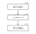
実施形態は、本明細書で開示するプロセス、機能および/またはアルゴリズムを実行するための様々な方法を含むことが諒解されよう。たとえば、図3に示すように、実施形態は、メモリアクセスに対する物理アドレスを指定するステップ(たとえば、命令120はビット208a、208b、および208cを含む物理アドレスを指定する)-ブロック302と、アドレス変換をバイパスするステップ(たとえば、DTLB 214をバイパスする)-ブロック304と、物理アドレスを使用してメモリアクセスを実行するステップ(たとえば、選択器216は、DTLB 214からの仮想から物理へのアドレス変換の代わりに、物理アドレスビット208a、208b、および208cを選択するように構成される)-ブロック306とを含むメモリ(たとえば、D-キャッシュ210)にアクセスするための方法を含み得る。
It will be appreciated that embodiments include various methods for performing the processes, functions and / or algorithms disclosed herein. For example, as shown in FIG. 3, the embodiment includes the step of specifying a physical address for memory access (eg,
情報および信号は、多種多様な技術および技法のいずれかを使用して表され得ることを当業者は諒解されよう。たとえば、上記の説明全体にわたって言及され得るデータ、命令、コマンド、情報、信号、ビット、シンボル、およびチップは、電圧、電流、電磁波、磁界または磁性粒子、光場または光学粒子、あるいはそれらの任意の組合せによって表され得る。 Those skilled in the art will appreciate that information and signals may be represented using any of a variety of different technologies and techniques. For example, data, instructions, commands, information, signals, bits, symbols, and chips that may be referred to throughout the above description are voltages, currents, electromagnetic waves, magnetic fields or magnetic particles, light fields or optical particles, or any of them Can be represented by a combination.
さらに、本明細書で開示した実施形態に関連して説明した様々な例示的な論理ブロック、モジュール、回路、およびアルゴリズムステップは、電子ハードウェア、コンピュータソフトウェア、または両方の組合せとして実装できることを、当業者は諒解されよう。ハードウェアとソフトウェアのこの互換性を明確に示すために、様々な例示的な構成要素、ブロック、モジュール、回路、およびステップを、上記では概してそれらの機能に関して説明した。そのような機能をハードウェアとして実装するか、またはソフトウェアとして実装するかは、特定の適用例および全体的なシステムに課される設計制約に依存する。当業者は、説明した機能を特定の適用例ごとに様々な方法で実装し得るが、そのような実装の決定は、本発明の範囲からの逸脱を生じるものと解釈すべきではない。 Further, it is understood that the various exemplary logic blocks, modules, circuits, and algorithm steps described in connection with the embodiments disclosed herein can be implemented as electronic hardware, computer software, or a combination of both. The contractor will be understood. To clearly illustrate this interchangeability of hardware and software, various illustrative components, blocks, modules, circuits, and steps have been described above generally in terms of their functionality. Whether such functionality is implemented as hardware or software depends upon the particular application and design constraints imposed on the overall system. Those skilled in the art may implement the described functionality in a variety of ways for each particular application, but such implementation decisions should not be construed as departing from the scope of the present invention.
本明細書で開示された実施形態と関連して説明された方法、シーケンス、および/またはアルゴリズムは、ハードウェアで、プロセッサによって実行されるソフトウェアモジュールで、またはその2つの組合せで直接具現化され得る。ソフトウェアモジュールは、RAMメモリ、フラッシュメモリ、ROMメモリ、EPROMメモリ、EEPROMメモリ、レジスタ、ハードディスク、リムーバブルディスク、CD-ROM、または当技術分野で知られている任意の他の形態の記憶媒体中に常駐し得る。例示的な記憶媒体は、プロセッサが記憶媒体から情報を読み取り、かつ記憶媒体に情報を書き込むことができるように、プロセッサに結合される。代替として、記憶媒体はプロセッサと一体であり得る。 The methods, sequences, and / or algorithms described in connection with the embodiments disclosed herein may be directly embodied in hardware, software modules executed by a processor, or a combination of the two. . Software modules reside in RAM memory, flash memory, ROM memory, EPROM memory, EEPROM memory, registers, hard disks, removable disks, CD-ROMs, or any other form of storage medium known in the art Can do. An exemplary storage medium is coupled to the processor such that the processor can read information from, and write information to, the storage medium. In the alternative, the storage medium may be integral to the processor.
図4を参照すると、例示的な実施形態に従って構成されたマルチコアプロセッサを含むワイヤレスデバイスの特定の例示的な実施形態のブロック図が示され、全体的に400と表される。デバイス400は、デジタル信号プロセッサ(DSP)464を含む。処理システム100と同様に、DSP 464は、図1のMMU 106と、レジスタファイル104を備えるプロセッサ102と、I-キャッシュ108と、D-キャッシュ110とを含み、それらは図示のメモリ432と結合され得る。デバイス400は、前述の実施形態で説明したように、仮想から物理へのアドレス変換を実行することなく、命令120と120'とを実行するように構成され得る。図4は、DSP464およびディスプレイ428に結合された、ディスプレイコントローラ426も示している。コーダ/デコーダ(CODEC)434(たとえば、オーディオおよび/または音声CODEC)は、DSP464に結合され得る。ワイヤレスコントローラ440(モデムを含むことができる)などの他の構成要素も示されている。スピーカ436およびマイクロフォン438は、CODEC434に結合され得る。図4は、ワイヤレスコントローラ440が、ワイヤレスアンテナ442に結合され得ることも示している。特定の一実施形態では、DSP464、ディスプレイコントローラ426、メモリ432、CODEC434、およびワイヤレスコントローラ440は、システムインパッケージまたはシステムオンチップデバイス422内に含まれる。
With reference to FIG. 4, a block diagram of a particular exemplary embodiment of a wireless device including a multi-core processor configured in accordance with the exemplary embodiment is shown and generally designated 400.
ある特定の実施形態では、入力デバイス430および電源444が、システムオンチップデバイス422に結合される。さらに、ある特定の実施形態では、図4に示すように、ディスプレイ428、入力デバイス430、スピーカ436、マイクロフォン438、ワイヤレスアンテナ442、および電源444は、システムオンチップデバイス422の外部にある。ただし、ディスプレイ428、入力デバイス430、スピーカ436、マイクロフォン438、ワイヤレスアンテナ442、および電源444の各々は、インターフェースまたはコントローラのような、システムオンチップデバイス422の構成要素に結合され得る。
In certain embodiments,
図4はワイヤレス通信デバイスを示しているが、DSP464およびメモリ432は、セットトップボックス、音楽プレーヤ、ビデオプレーヤ、娯楽ユニット、ナビゲーションデバイス、携帯情報端末(PDA)、固定ロケーションデータユニット、またはコンピュータ内に組み込むこともできることに留意されたい。プロセッサ(たとえばDSP464)も、そのようなデバイス内に組み込むことができる。
Although FIG. 4 shows a wireless communication device, the
したがって、本発明の一実施形態は、物理アドレスを使用してメモリにアクセスし、仮想から物理へのアドレス変換のために構成されたMMUをバイパスするための方法を具現するコンピュータ可読媒体を含み得る。したがって、本発明は図示の例に限定されず、本明細書で説明した機能を実行するためのいかなる手段も、本発明の実施形態中に含まれる。 Accordingly, one embodiment of the present invention may include a computer readable medium embodying a method for accessing a memory using a physical address and bypassing an MMU configured for virtual to physical address translation. . Accordingly, the present invention is not limited to the illustrated examples, and any means for performing the functions described herein are included in embodiments of the present invention.
上記の開示は本発明の例示的な実施形態を示すが、添付の特許請求の範囲によって規定される本発明の範囲から逸脱することなく、本明細書において様々な変更および修正を行えることに留意されたい。本明細書で説明された本発明の実施形態による方法クレームの機能、ステップおよび/または動作は、特定の順序で実行されなくてもよい。さらに、本発明の要素は、単数形で説明または請求されていることがあるが、単数形に限定することが明示的に述べられていない限り、複数形が企図される。 While the above disclosure illustrates exemplary embodiments of the present invention, it is noted that various changes and modifications can be made herein without departing from the scope of the present invention as defined by the appended claims. I want to be. The functions, steps and / or actions of a method claim according to embodiments of the invention described herein may not be performed in a particular order. Further, although elements of the invention may be described or claimed in the singular, the plural is contemplated unless expressly stated to be limited to the singular.
100 処理システム
102 プロセッサ
104 レジスタファイル
106 メモリ管理ユニット(MMU)
108 I-キャッシュ
110 D-キャッシュ
112 メインメモリ
114 仮想計算機マネージャ(VMM)
116 ゲスト
120 メモリアクセス命令
202 タグアレイ
204 状態アレイ
206 置き換えポインタアレイ
208a PA[タグビット]
208b PA[セットビット]
208c PA[データアレイビット]
210 データアレイ
214 DTLB
216 コマンドSelect PA Directly
218 比較器
220 ヒット/ミスライン
222 ライトデータアレイ
224 リードデータライン
400 マルチコアプロセッサを含むワイヤレスデバイスのブロック図
422 システムインパッケージまたはシステムオンチップデバイス
426 ディスプレイコントローラ
428 ディスプレイ
430 入力デバイス
432 メモリ
434 コーダ/デコーダ(CODEC)
436 スピーカ
438 マイクロフォン
440 ワイヤレスコントローラ
442 ワイヤレスアンテナ
444 電源
464 デジタル信号プロセッサ(DSP)
100 treatment system
102 processor
104 Register file
106 Memory management unit (MMU)
108 I-Cash
110 D-cache
112 Main memory
114 Virtual Machine Manager (VMM)
116 guests
120 Memory access instruction
202 tag array
204 state array
206 Replacement pointer array
208a PA [Tag Bit]
208b PA [Set bit]
208c PA [Data array bit]
210 Data array
214 DTLB
216 Command Select PA Directly
218 Comparator
220 hit / miss line
222 Write data array
224 Read data line
Block diagram of a wireless device containing 400 multi-core processors
422 System in package or system on chip device
426 display controller
428 display
430 input devices
432 memory
434 Coder / Decoder (CODEC)
436 speaker
438 microphone
440 wireless controller
442 Wireless antenna
444 power supply
464 Digital Signal Processor (DSP)
Claims (13)
プロセッサによってメモリアクセス要求を開始するステップと、
前記メモリアクセスに対する物理アドレスを指定するステップと、
仮想から物理へのアドレス変換をバイパスするステップと、
前記物理アドレスに基づいて前記プロセッサと前記メモリとの間で構成される1つまたは複数のレベルのキャッシュをトラバースするステップと、
ミスが遭遇される任意の中間キャッシュレベルのキャッシュ状態を変更することなく、前記物理アドレスを使用してヒットが最初に遭遇された前記キャッシュレベルまたはメモリから前記メモリアクセスを実行するステップとを含む、方法。 A method for accessing memory, comprising:
Initiating a memory access request by the processor;
Designating a physical address for the memory access;
Bypassing virtual to physical address translation;
Traversing one or more levels of cache configured between the processor and the memory based on the physical address;
Performing the memory access from the cache level or memory where a hit was first encountered using the physical address without changing the cache state of any intermediate cache level where a miss is encountered; Method.
前記メモリアクセスを実行するステップが、前記ヒットが最初に遭遇された前記キャッシュレベルまたはメモリから前記プロセッサに直接前記物理アドレスに関連するデータを返すステップを含む、請求項1に記載の方法。 The memory access is a load request;
2. The method of claim 1, wherein performing the memory access comprises returning data associated with the physical address directly from the cache level or memory where the hit was first encountered to the processor.
前記メモリアクセスを実行するステップが、前記ヒットが最初に遭遇された前記キャッシュレベルまたはメモリに前記プロセッサから直接前記ストア要求に関連するデータを書き込むステップを含む、請求項1に記載の方法。 The memory access is a store request;
It said step of performing a memory access includes the step of writing the Lud over data related to the store request directly from the processor in the cache level or memory the hit is encountered first, the method according to claim 1 .
メモリと、
仮想から物理にアドレスを変換するように構成された変換ルックアサイドバッファ(TLB)と、
関連する物理アドレスを指定するメモリアクセス命令が前記プロセッサによって開始されることに応答して、
前記メモリアクセス命令に対する仮想から物理へのアドレス変換をバイパスし、
前記物理アドレスに基づいて前記プロセッサと前記メモリとの間で構成される1つまたは複数のレベルのキャッシュをトラバースし、
ミスが遭遇される任意の中間キャッシュレベルのキャッシュ状態を変更することなく、前記物理アドレスを用いてヒットが最初に遭遇された前記キャッシュレベルまたはメモリから前記メモリアクセスを実行する
ように構成された実行論理部とを備える、処理システム。 A processor with a register file;
Memory,
A translation lookaside buffer (TLB) configured to translate addresses from virtual to physical;
In response to a memory access instruction specifying an associated physical address being initiated by the processor,
Bypass virtual to physical address translation for the memory access instructions;
Traverse one or more levels of cache configured between the processor and the memory based on the physical address;
Execution configured to perform the memory access from the cache level or memory where a hit was first encountered using the physical address without changing the cache state of any intermediate cache level where a miss is encountered A processing system comprising a logic unit.
Applications Claiming Priority (5)
| Application Number | Priority Date | Filing Date | Title |
|---|---|---|---|
| US201261584964P | 2012-01-10 | 2012-01-10 | |
| US61/584,964 | 2012-01-10 | ||
| US13/398,927 | 2012-02-17 | ||
| US13/398,927 US20130179642A1 (en) | 2012-01-10 | 2012-02-17 | Non-Allocating Memory Access with Physical Address |
| PCT/US2013/021050 WO2013106583A1 (en) | 2012-01-10 | 2013-01-10 | Non-allocating memory access with physical address |
Publications (3)
| Publication Number | Publication Date |
|---|---|
| JP2015503805A JP2015503805A (en) | 2015-02-02 |
| JP2015503805A5 JP2015503805A5 (en) | 2017-04-13 |
| JP6133896B2 true JP6133896B2 (en) | 2017-05-24 |
Family
ID=48744770
Family Applications (1)
| Application Number | Title | Priority Date | Filing Date |
|---|---|---|---|
| JP2014551429A Expired - Fee Related JP6133896B2 (en) | 2012-01-10 | 2013-01-10 | Unallocated memory access using physical addresses |
Country Status (6)
| Country | Link |
|---|---|
| US (1) | US20130179642A1 (en) |
| EP (1) | EP2802993A1 (en) |
| JP (1) | JP6133896B2 (en) |
| KR (1) | KR20140110070A (en) |
| CN (1) | CN104067246B (en) |
| WO (1) | WO2013106583A1 (en) |
Families Citing this family (22)
| Publication number | Priority date | Publication date | Assignee | Title |
|---|---|---|---|---|
| US9645941B2 (en) * | 2013-09-26 | 2017-05-09 | Cavium, Inc. | Collapsed address translation with multiple page sizes |
| US9208103B2 (en) * | 2013-09-26 | 2015-12-08 | Cavium, Inc. | Translation bypass in multi-stage address translation |
| US9268694B2 (en) | 2013-09-26 | 2016-02-23 | Cavium, Inc. | Maintenance of cache and tags in a translation lookaside buffer |
| US9639476B2 (en) * | 2013-09-26 | 2017-05-02 | Cavium, Inc. | Merged TLB structure for multiple sequential address translations |
| US20150161057A1 (en) * | 2013-12-05 | 2015-06-11 | Qualcomm Incorporated | System and method for providing client-side address translation in a memory management system |
| WO2016064403A1 (en) * | 2014-10-23 | 2016-04-28 | Hewlett Packard Enterprise Development Lp | Supervisory memory management unit |
| US20160210231A1 (en) * | 2015-01-21 | 2016-07-21 | Mediatek Singapore Pte. Ltd. | Heterogeneous system architecture for shared memory |
| GB2536880B (en) * | 2015-03-24 | 2021-07-28 | Advanced Risc Mach Ltd | Memory management |
| US10078597B2 (en) * | 2015-04-03 | 2018-09-18 | Via Alliance Semiconductor Co., Ltd. | System and method of distinguishing system management mode entries in a translation address cache of a processor |
| US10180908B2 (en) * | 2015-05-13 | 2019-01-15 | Qualcomm Incorporated | Method and apparatus for virtualized control of a shared system cache |
| US9672159B2 (en) * | 2015-07-02 | 2017-06-06 | Arm Limited | Translation buffer unit management |
| US10223289B2 (en) * | 2015-07-07 | 2019-03-05 | Qualcomm Incorporated | Secure handling of memory caches and cached software module identities for a method to isolate software modules by means of controlled encryption key management |
| US20170046158A1 (en) * | 2015-08-14 | 2017-02-16 | Qualcomm Incorporated | Determining prefetch instructions based on instruction encoding |
| US10019380B2 (en) * | 2015-09-25 | 2018-07-10 | Qualcomm Incorporated | Providing memory management functionality using aggregated memory management units (MMUs) |
| US10102168B2 (en) * | 2016-02-09 | 2018-10-16 | Avago Technologies General Ip (Singapore) Pte. Ltd. | Scalable low-latency mesh interconnect for switch chips |
| DE102017000530B4 (en) | 2016-02-09 | 2023-12-21 | Avago Technologies International Sales Pte. Limited | Scalable, low-latency machine network interconnection structure for switch chips |
| US20170255569A1 (en) * | 2016-03-01 | 2017-09-07 | Qualcomm Incorporated | Write-allocation for a cache based on execute permissions |
| US9823854B2 (en) * | 2016-03-18 | 2017-11-21 | Qualcomm Incorporated | Priority-based access of compressed memory lines in memory in a processor-based system |
| US11221971B2 (en) | 2016-04-08 | 2022-01-11 | Qualcomm Incorporated | QoS-class based servicing of requests for a shared resource |
| US10482021B2 (en) * | 2016-06-24 | 2019-11-19 | Qualcomm Incorporated | Priority-based storage and access of compressed memory lines in memory in a processor-based system |
| US10061698B2 (en) * | 2017-01-31 | 2018-08-28 | Qualcomm Incorporated | Reducing or avoiding buffering of evicted cache data from an uncompressed cache memory in a compression memory system when stalled write operations occur |
| CN116431530B (en) * | 2023-02-08 | 2024-03-15 | 北京超弦存储器研究院 | CXL memory module, memory processing method and computer system |
Family Cites Families (33)
| Publication number | Priority date | Publication date | Assignee | Title |
|---|---|---|---|---|
| US5307477A (en) * | 1989-12-01 | 1994-04-26 | Mips Computer Systems, Inc. | Two-level cache memory system |
| DE4323929A1 (en) * | 1992-10-13 | 1994-04-14 | Hewlett Packard Co | Software-managed, multi-level cache storage system |
| US5623632A (en) * | 1995-05-17 | 1997-04-22 | International Business Machines Corporation | System and method for improving multilevel cache performance in a multiprocessing system |
| US5742840A (en) * | 1995-08-16 | 1998-04-21 | Microunity Systems Engineering, Inc. | General purpose, multiple precision parallel operation, programmable media processor |
| US5740399A (en) * | 1995-08-23 | 1998-04-14 | International Business Machines Corporation | Modified L1/L2 cache inclusion for aggressive prefetch |
| US6085291A (en) * | 1995-11-06 | 2000-07-04 | International Business Machines Corporation | System and method for selectively controlling fetching and prefetching of data to a processor |
| US5737751A (en) * | 1996-03-26 | 1998-04-07 | Intellectual Business Machines Corporation | Cache memory management system having reduced reloads to a second level cache for enhanced memory performance in a data processing system |
| US5956507A (en) * | 1996-05-14 | 1999-09-21 | Shearer, Jr.; Bennie L. | Dynamic alteration of operating system kernel resource tables |
| US5892970A (en) * | 1996-07-01 | 1999-04-06 | Sun Microsystems, Inc. | Multiprocessing system configured to perform efficient block copy operations |
| US5983332A (en) * | 1996-07-01 | 1999-11-09 | Sun Microsystems, Inc. | Asynchronous transfer mode (ATM) segmentation and reassembly unit virtual address translation unit architecture |
| US5960465A (en) * | 1997-02-27 | 1999-09-28 | Novell, Inc. | Apparatus and method for directly accessing compressed data utilizing a compressed memory address translation unit and compression descriptor table |
| US6014740A (en) * | 1997-04-11 | 2000-01-11 | Bmc Software, Inc. | Single instruction method of seizing control of program execution flow in a multiprocessor computer system |
| US6145054A (en) * | 1998-01-21 | 2000-11-07 | Sun Microsystems, Inc. | Apparatus and method for handling multiple mergeable misses in a non-blocking cache |
| US6341325B2 (en) * | 1999-01-12 | 2002-01-22 | International Business Machines Corporation | Method and apparatus for addressing main memory contents including a directory structure in a computer system |
| US6385712B1 (en) * | 1999-10-25 | 2002-05-07 | Ati International Srl | Method and apparatus for segregation of virtual address space |
| US6625714B1 (en) * | 1999-12-17 | 2003-09-23 | Hewlett-Packard Development Company, L.P. | Parallel distributed function translation lookaside buffer |
| US6741258B1 (en) * | 2000-01-04 | 2004-05-25 | Advanced Micro Devices, Inc. | Distributed translation look-aside buffers for graphics address remapping table |
| US6711653B1 (en) * | 2000-03-30 | 2004-03-23 | Intel Corporation | Flexible mechanism for enforcing coherency among caching structures |
| US6549997B2 (en) * | 2001-03-16 | 2003-04-15 | Fujitsu Limited | Dynamic variable page size translation of addresses |
| US6889308B1 (en) * | 2002-01-18 | 2005-05-03 | Advanced Micro Devices, Inc. | Method and apparatus for protecting page translations |
| JP4220476B2 (en) * | 2002-11-18 | 2009-02-04 | エイアールエム リミテッド | Virtual-physical memory address mapping in systems with secure and non-secure domains |
| US20040193833A1 (en) * | 2003-03-27 | 2004-09-30 | Kathryn Hampton | Physical mode addressing |
| US7076635B1 (en) * | 2003-09-04 | 2006-07-11 | Advanced Micro Devices, Inc. | Method and apparatus for reducing instruction TLB accesses |
| US7302528B2 (en) * | 2004-11-19 | 2007-11-27 | Intel Corporation | Caching bypass |
| US9280473B2 (en) * | 2004-12-02 | 2016-03-08 | Intel Corporation | Method and apparatus for accessing physical memory from a CPU or processing element in a high performance manner |
| US7237065B2 (en) * | 2005-05-24 | 2007-06-26 | Texas Instruments Incorporated | Configurable cache system depending on instruction type |
| JP5076411B2 (en) * | 2005-11-30 | 2012-11-21 | ソニー株式会社 | Storage device, computer system |
| US7376807B2 (en) * | 2006-02-23 | 2008-05-20 | Freescale Semiconductor, Inc. | Data processing system having address translation bypass and method therefor |
| US20080229026A1 (en) * | 2007-03-15 | 2008-09-18 | Taiwan Semiconductor Manufacturing Co., Ltd. | System and method for concurrently checking availability of data in extending memories |
| US9710384B2 (en) * | 2008-01-04 | 2017-07-18 | Micron Technology, Inc. | Microprocessor architecture having alternative memory access paths |
| JP2009093559A (en) * | 2007-10-11 | 2009-04-30 | Nec Corp | Processor, information processing device and cache control method of processor |
| US8145874B2 (en) * | 2008-02-26 | 2012-03-27 | Qualcomm Incorporated | System and method of data forwarding within an execution unit |
| US8185692B2 (en) * | 2009-02-09 | 2012-05-22 | Oracle America, Inc. | Unified cache structure that facilitates accessing translation table entries |
-
2012
- 2012-02-17 US US13/398,927 patent/US20130179642A1/en not_active Abandoned
-
2013
- 2013-01-10 JP JP2014551429A patent/JP6133896B2/en not_active Expired - Fee Related
- 2013-01-10 WO PCT/US2013/021050 patent/WO2013106583A1/en active Application Filing
- 2013-01-10 CN CN201380005026.9A patent/CN104067246B/en not_active Expired - Fee Related
- 2013-01-10 KR KR1020147022169A patent/KR20140110070A/en not_active Application Discontinuation
- 2013-01-10 EP EP13700444.6A patent/EP2802993A1/en not_active Withdrawn
Also Published As
| Publication number | Publication date |
|---|---|
| WO2013106583A1 (en) | 2013-07-18 |
| JP2015503805A (en) | 2015-02-02 |
| CN104067246B (en) | 2018-07-03 |
| KR20140110070A (en) | 2014-09-16 |
| EP2802993A1 (en) | 2014-11-19 |
| CN104067246A (en) | 2014-09-24 |
| US20130179642A1 (en) | 2013-07-11 |
Similar Documents
| Publication | Publication Date | Title |
|---|---|---|
| JP6133896B2 (en) | Unallocated memory access using physical addresses | |
| US9619387B2 (en) | Invalidating stored address translations | |
| US11650926B2 (en) | Virtual cache synonym detection using alias tags | |
| JP6081672B2 (en) | Efficient address translation caching in processors that support many different address spaces | |
| KR101587361B1 (en) | Merged TLB Structure for Multiple Sequential Address Translations | |
| KR101598353B1 (en) | translation bypass in multi-stage address translation | |
| US9465748B2 (en) | Instruction fetch translation lookaside buffer management to support host and guest O/S translations | |
| JP5680642B2 (en) | IOMMU with two-level address translation for I / O and computational load reduction devices in peripheral interconnects | |
| US9645941B2 (en) | Collapsed address translation with multiple page sizes | |
| US9436616B2 (en) | Multi-core page table sets of attribute fields | |
| US9367470B2 (en) | Bounded cache searches | |
| JP6960933B2 (en) | Write-Allocation of Cache Based on Execution Permission | |
| US20110023027A1 (en) | I/o memory management unit including multilevel address translation for i/o and computation offload | |
| JP2015503805A5 (en) | ||
| KR20130048191A (en) | Address mapping in virtualized processing system | |
| TWI641947B (en) | Method and apparatus for managing address translation and caching | |
| US20180157601A1 (en) | Apparatus and method for avoiding conflicting entries in a storage structure | |
| TW201633145A (en) | Managing reuse information for memory pages | |
| JP7449694B2 (en) | Configurable skew associativity in translation index buffers | |
| TW201633137A (en) | Managing reuse information with multiple translation stages | |
| JP7155629B2 (en) | Arithmetic processing device, information processing device, and method of controlling arithmetic processing device | |
| US8527736B1 (en) | Systems and methods for improving address translation speed |
Legal Events
| Date | Code | Title | Description |
|---|---|---|---|
| A521 | Written amendment |
Free format text: JAPANESE INTERMEDIATE CODE: A523 Effective date: 20151210 |
|
| A621 | Written request for application examination |
Free format text: JAPANESE INTERMEDIATE CODE: A621 Effective date: 20151210 |
|
| A977 | Report on retrieval |
Free format text: JAPANESE INTERMEDIATE CODE: A971007 Effective date: 20161128 |
|
| A131 | Notification of reasons for refusal |
Free format text: JAPANESE INTERMEDIATE CODE: A131 Effective date: 20161212 |
|
| A524 | Written submission of copy of amendment under section 19 (pct) |
Free format text: JAPANESE INTERMEDIATE CODE: A524 Effective date: 20170307 |
|
| TRDD | Decision of grant or rejection written | ||
| A01 | Written decision to grant a patent or to grant a registration (utility model) |
Free format text: JAPANESE INTERMEDIATE CODE: A01 Effective date: 20170327 |
|
| A61 | First payment of annual fees (during grant procedure) |
Free format text: JAPANESE INTERMEDIATE CODE: A61 Effective date: 20170420 |
|
| R150 | Certificate of patent or registration of utility model |
Ref document number: 6133896 Country of ref document: JP Free format text: JAPANESE INTERMEDIATE CODE: R150 |
|
| R250 | Receipt of annual fees |
Free format text: JAPANESE INTERMEDIATE CODE: R250 |
|
| LAPS | Cancellation because of no payment of annual fees |