JP6133280B2 - Single switch driver device with LC filter for driving load, especially LED unit - Google Patents
Single switch driver device with LC filter for driving load, especially LED unit Download PDFInfo
- Publication number
- JP6133280B2 JP6133280B2 JP2014515319A JP2014515319A JP6133280B2 JP 6133280 B2 JP6133280 B2 JP 6133280B2 JP 2014515319 A JP2014515319 A JP 2014515319A JP 2014515319 A JP2014515319 A JP 2014515319A JP 6133280 B2 JP6133280 B2 JP 6133280B2
- Authority
- JP
- Japan
- Prior art keywords
- power
- coupled
- driver device
- output terminal
- voltage
- Prior art date
- Legal status (The legal status is an assumption and is not a legal conclusion. Google has not performed a legal analysis and makes no representation as to the accuracy of the status listed.)
- Active
Links
- 239000003990 capacitor Substances 0.000 claims description 59
- 238000006243 chemical reaction Methods 0.000 claims description 44
- 238000005286 illumination Methods 0.000 claims description 5
- 230000000712 assembly Effects 0.000 claims 1
- 238000000429 assembly Methods 0.000 claims 1
- 238000010586 diagram Methods 0.000 description 14
- 238000007781 pre-processing Methods 0.000 description 10
- 238000001914 filtration Methods 0.000 description 4
- 230000006870 function Effects 0.000 description 4
- 238000000034 method Methods 0.000 description 3
- 238000003860 storage Methods 0.000 description 3
- 238000013459 approach Methods 0.000 description 2
- 230000007423 decrease Effects 0.000 description 2
- 230000001419 dependent effect Effects 0.000 description 2
- 238000013461 design Methods 0.000 description 2
- 241001672648 Vieira Species 0.000 description 1
- 230000008901 benefit Effects 0.000 description 1
- 230000008859 change Effects 0.000 description 1
- 230000001010 compromised effect Effects 0.000 description 1
- 238000012937 correction Methods 0.000 description 1
- 230000008878 coupling Effects 0.000 description 1
- 238000010168 coupling process Methods 0.000 description 1
- 238000005859 coupling reaction Methods 0.000 description 1
- 238000002955 isolation Methods 0.000 description 1
- 238000004519 manufacturing process Methods 0.000 description 1
- 230000008447 perception Effects 0.000 description 1
- 239000013641 positive control Substances 0.000 description 1
- 230000004044 response Effects 0.000 description 1
- 238000005549 size reduction Methods 0.000 description 1
Images


Classifications
-
- H—ELECTRICITY
- H05—ELECTRIC TECHNIQUES NOT OTHERWISE PROVIDED FOR
- H05B—ELECTRIC HEATING; ELECTRIC LIGHT SOURCES NOT OTHERWISE PROVIDED FOR; CIRCUIT ARRANGEMENTS FOR ELECTRIC LIGHT SOURCES, IN GENERAL
- H05B45/00—Circuit arrangements for operating light-emitting diodes [LED]
- H05B45/30—Driver circuits
- H05B45/37—Converter circuits
- H05B45/3725—Switched mode power supply [SMPS]
- H05B45/375—Switched mode power supply [SMPS] using buck topology
-
- H—ELECTRICITY
- H05—ELECTRIC TECHNIQUES NOT OTHERWISE PROVIDED FOR
- H05B—ELECTRIC HEATING; ELECTRIC LIGHT SOURCES NOT OTHERWISE PROVIDED FOR; CIRCUIT ARRANGEMENTS FOR ELECTRIC LIGHT SOURCES, IN GENERAL
- H05B45/00—Circuit arrangements for operating light-emitting diodes [LED]
- H05B45/30—Driver circuits
- H05B45/37—Converter circuits
- H05B45/3725—Switched mode power supply [SMPS]
- H05B45/385—Switched mode power supply [SMPS] using flyback topology
-
- Y—GENERAL TAGGING OF NEW TECHNOLOGICAL DEVELOPMENTS; GENERAL TAGGING OF CROSS-SECTIONAL TECHNOLOGIES SPANNING OVER SEVERAL SECTIONS OF THE IPC; TECHNICAL SUBJECTS COVERED BY FORMER USPC CROSS-REFERENCE ART COLLECTIONS [XRACs] AND DIGESTS
- Y02—TECHNOLOGIES OR APPLICATIONS FOR MITIGATION OR ADAPTATION AGAINST CLIMATE CHANGE
- Y02B—CLIMATE CHANGE MITIGATION TECHNOLOGIES RELATED TO BUILDINGS, e.g. HOUSING, HOUSE APPLIANCES OR RELATED END-USER APPLICATIONS
- Y02B20/00—Energy efficient lighting technologies, e.g. halogen lamps or gas discharge lamps
- Y02B20/30—Semiconductor lamps, e.g. solid state lamps [SSL] light emitting diodes [LED] or organic LED [OLED]
Description
本発明は、負荷、特に一つ又は複数のLEDを備えるLEDユニットを駆動するためのドライバ装置に関する。また、本発明は照明装置に関する。 The present invention relates to a driver device for driving a load, in particular an LED unit comprising one or more LEDs. The present invention also relates to a lighting device.
レトロフィットランプ等のオフラインアプリケーション用のLEDドライバの分野において、高効率性、高電力密度、長寿命、高力率、及び低コスト等の特徴に対応するソリューションが求められている。既存のソリューションのほぼ全てがこれらの要件のいずれかを満たしているが、提案されるドライバ回路は、現在及び将来のコンセント(電源)規格に適合しつつ、コンセント電力の形式をLEDに適した形式に適切に調整しなければならない。力率を所定の下限以上に維持するとともに、最大光知覚フリッカーを保証する(好ましくはゼロ)ことは極めて重要である。 In the field of LED drivers for off-line applications such as retrofit lamps, there is a need for solutions that address features such as high efficiency, high power density, long life, high power factor, and low cost. Almost all existing solutions meet any of these requirements, but the proposed driver circuit is compatible with current and future outlet (power) standards, while the outlet power type is suitable for LEDs. Must be adjusted appropriately. It is extremely important to maintain the power factor above a predetermined lower limit and to ensure maximum light perception flicker (preferably zero).
また、オフラインコンバータにおいて高力率及び低高調波歪を実現するためには、コンセントからのエネルギーを、供給される電圧波形に比例して同期的に引き出さなければならない場合が多い。このタスクを、負荷に送られるエネルギーの形式を不適切に損なうことなく最適に達成するために、従来、独立した前処理(事前調整)段階を有する電力コンバータアーキテクチャが用いられてきた。 Further, in order to realize a high power factor and low harmonic distortion in an off-line converter, it is often necessary to extract energy from an outlet synchronously in proportion to a supplied voltage waveform. Traditionally, power converter architectures with independent pre-processing (preconditioning) stages have been used to optimally accomplish this task without undue loss of the type of energy delivered to the load.
典型的には、電源サイクル(又は供給サイクル、すなわち、電源電圧又は供給電圧のサイクル)を通して出力電力を一定に保ちつつ高力率を得るために、二段階の直列電力段が用いられる。これらのアーキテクチャにおいて、第一段階は電源電流を適合(変調)させ、第二段階は負荷への電力変換を行う。 Typically, a two-stage series power stage is used to obtain a high power factor while keeping the output power constant throughout the power cycle (or supply cycle, ie, the supply voltage or supply voltage cycle). In these architectures, the first stage adapts (modulates) the supply current and the second stage performs power conversion to the load.
しかし、複雑さ及びコストに関する理由から、二段階のうちの一つが本質的には必要ではない、従来「単段式」として知られる単純化されたパワートレイン(伝動機構)ソリューションが採用されている。このような単純化の結果、上記要求事項が大きく損なわれる可能性があり、且つ/又は、コンバータの性能が、特にサイズ、信頼性、及び寿命に関して、大きく低下する可能性がある。後者については、通常、一定の出力電力供給を保証する場合、負荷に並列な大きな低周波保持容量を用いなければならないことに主に起因する。 However, for reasons of complexity and cost, a simplified powertrain solution known as a “single stage” is employed, where one of the two stages is not essentially necessary. . As a result of such simplification, the above requirements can be severely compromised and / or the performance of the converter can be significantly degraded, particularly with respect to size, reliability, and lifetime. The latter is mainly due to the fact that usually a large low frequency holding capacitor in parallel with the load must be used to guarantee a constant output power supply.
単段式のソリューションに関する文献は一般的である。一例は、Robert Erickson、Michael Madigan著、「フライバックコンバータに基づく単純な高力率整流器の設計」、応用パワーエレクトロニクス会議及び展示会IEEE議事録、1990、pp.792−801である。 The literature on single-stage solutions is common. One example is Robert Ericsson, Michael Madigan, “Designing a Simple High Power Factor Rectifier Based on a Flyback Converter,” Applied Power Electronics Conference and Exhibition, IEEE Proceedings, 1990, pp. 11-27. 792-801.
二段式アプローチと単段式アプローチとの間にある中間ソリューションは、組み込まれた前処理段階を有する単段式コンバータである。このようなソリューションは、負荷及び電源(コンセント)の要求事項を満たしつつ、部品数の削減及び高電力密度を提供する。単一の電力変換段階を有する他の実施形態は、不連続導通モードで動作する昇圧コンバータを組み込むことで高力率(high power factors(HPF))を実現する。これらのコンバータは、実際には前述の二つの電力変換段階を組み合わせる。 An intermediate solution between the two-stage approach and the single-stage approach is a single-stage converter with an integrated pre-processing stage. Such a solution provides reduced component count and high power density while meeting load and power supply (outlet) requirements. Other embodiments having a single power conversion stage achieve high power factor (HPF) by incorporating a boost converter operating in discontinuous conduction mode. These converters actually combine the two power conversion stages described above.
「一定DCリンク電圧を有する高力率電子安定器」、Ricardo de Oliveira Brioschi、Jose Luiz F.Vieira著、パワーエレクトロニクスIEEE議事録、vol.13、no.6、1998には、コンパクトな蛍光ランプ用のHPFコンバータが記載されている。この例では、ハーフブリッジが、昇圧コンバータとLC並列共振コンバータとによって共有され、LC並列共振コンバータは、ゼロ電圧スイッチング(zero voltage switching (ZVS))を得るために共振以上で動作する。ZVSをさらにサポートするために、バス電圧は一定に制御される。しかし、このようなHPFコンバータは、通常大きなバス容量及び出力整流器を必要とし、電源電圧幅及び負荷(駆動)電圧幅が狭い。 "High power factor electronic ballast with constant DC link voltage", Richard de Oliveira Brioschi, Jose Luiz F. Vieira, Power Electronics IEEE Minutes, vol. 13, no. 6, 1998 describes a compact HPF converter for fluorescent lamps. In this example, the half bridge is shared by the boost converter and the LC parallel resonant converter, and the LC parallel resonant converter operates above resonance in order to obtain zero voltage switching (ZVS). In order to further support ZVS, the bus voltage is controlled constant. However, such an HPF converter usually requires a large bus capacity and an output rectifier, and has a narrow power supply voltage width and load (drive) voltage width.
R.Venkatraman、A.K.S.Bhat、Mark Edmunds著、「高調波歪が低減されたソフトスイッチング単段式AC−DCコンバータ」、エアロスペース及びエレクトロニクスシステムIEEE議事録、vol.36、no.4、2000年10月は、統合電力段階の他の例を示す。この文献は、一定電源負荷のために、高周波変圧器が分離した、ゼロ電圧スイッチング(ZVS)、高力率及び低高調波歪を有する単段式AC−DCコンバータを提示し、考察する。 R. Venkatraman, A.M. K. S. Bhat, Mark Edmunds, “Soft switching single-stage AC-DC converter with reduced harmonic distortion”, Aerospace and Electronics System IEEE Proceedings, vol. 36, no. 4, October 2000 shows another example of the integrated power stage. This document presents and discusses a single stage AC-DC converter with zero voltage switching (ZVS), high power factor and low harmonic distortion, separated by a high frequency transformer for constant power loads.
本発明の目的は、負荷、特に一つ以上のLEDを有するLEDユニットを駆動するためのドライバ装置を提供することであり、とりわけ高力率、実質的に一定負荷、小サイズ、高効率性、長寿命、及び低コストを提供するドライバ装置を提供することである。また、本発明の他の目的は、対応する照明装置を提供することである。 The object of the present invention is to provide a driver device for driving a load, in particular an LED unit having one or more LEDs, in particular a high power factor, a substantially constant load, a small size, a high efficiency, It is an object of the present invention to provide a driver device that provides long life and low cost. Another object of the present invention is to provide a corresponding lighting device.
本発明の一側面によれば、
負荷、特に一つ以上のLEDを含むLEDユニット用のドライバ装置であって、
外部電源から整流電源電圧を受ける電力入力端子と、
負荷を駆動するための駆動電圧及び/又は電流を供給する電力出力端子と、
いずれもスイッチノードに結合された単一のスイッチング要素とエネルギー保持要素とを含む、前記電力入力端子に結合された単段式電力変換ユニットであって、前記電力出力端子は単段式電力変換ユニットの出力部によって表される、前記単段式電力変換ユニットと、
前記スイッチノードに結合された、フィルタインダクタとフィルタコンデンサとを含むフィルタユニットと、
前記スイッチング要素を制御する制御ユニットと
を有する、ドライバ装置が提供される。
According to one aspect of the invention,
A driver device for a load, in particular an LED unit comprising one or more LEDs,
A power input terminal for receiving a rectified power supply voltage from an external power supply;
A power output terminal for supplying a driving voltage and / or current for driving a load;
A single stage power conversion unit coupled to the power input terminal, both including a single switching element and an energy holding element coupled to a switch node, wherein the power output terminal is a single stage power conversion unit The single-stage power conversion unit represented by the output of
A filter unit coupled to the switch node and including a filter inductor and a filter capacitor;
And a control unit for controlling the switching element.
本発明の他の側面によれば、一つ以上の照明ユニットを含む照明アセンブリ、特に一つ以上のLEDを含むLEDユニットと、前記照明アセンブリを駆動する本発明が提供するドライバ装置とを有する照明装置が提供される。 According to another aspect of the present invention, an illumination assembly comprising one or more illumination units, in particular an LED unit comprising one or more LEDs, and a driver device provided by the present invention for driving the illumination assembly. An apparatus is provided.
本発明の実施形態は、従属請求項において定義される。上記照明装置は、上記装置の従属請求項において定義される実施形態と同様及び/又は同一の好適な実施形態を有する。 Embodiments of the invention are defined in the dependent claims. The lighting device has a preferred embodiment similar to and / or identical to the embodiment defined in the dependent claims of the device.
本発明は、一定な出力電力を負荷に送達する一方で高力率を達成する、前処理ユニットが組み込まれた単段式電力コンバータ(電力変換ユニット)を提供するという着想に基づく。これは、フィルタユニットの要素によって表されるローパスフィルタが組み込まれた電力コンバータを適切に制御することによって実現される。通常、変換機能を実施するには単一のスイッチしか必要とされない。提案されるドライバ装置は、特に電力出力端子に結合された高電圧LEDストリングを使用するオフラインLEDドライバを対象とする。 The present invention is based on the idea of providing a single stage power converter (power conversion unit) incorporating a pre-processing unit that delivers constant output power to a load while achieving a high power factor. This is achieved by appropriately controlling a power converter incorporating a low pass filter represented by the elements of the filter unit. Usually only a single switch is required to perform the conversion function. The proposed driver device is particularly intended for off-line LED drivers that use high voltage LED strings coupled to power output terminals.
LED用の二段式オフラインドライバと比較して、高コスト、複雑性、及び大きな部品数という、電源及び負荷の両方の要求事項を満たすための課題が解決される。これは、提案されるドライバ装置及び方法が、慣用的な部品を好適に用いながら、単純性及び少部品数を備えることによる。 Compared to a two-stage offline driver for LEDs, the problem of meeting both power supply and load requirements of high cost, complexity and large number of parts is solved. This is due to the fact that the proposed driver apparatus and method provides simplicity and a small number of parts while preferably using conventional parts.
LED用の単段式オフラインドライバと比較して、下記の問題が解決される。出力電力を一定に保ちながら、電源サイクル又はコンセントサイクル間の低周波保持容量電圧変動を小さくする(例えば、20〜80%)ことによって、大きな低周波コンデンサを省くことができる。これは、サイズの小型化、並びに特に高温動作における長寿命及び高信頼性につながる。また、電源及び負荷のいずれの要求事項も損なうことなく部品数を削減することが必要である。これは、電力段(パワーステージ)及び電力段に組み込まれた前処理機能の動作によって本質的に達成される。また、大きな低周波保持容量を用いたとしても、単段式では知覚フリッカーを完全に排除できないおそれがある。提案されるソリューションは、一定出力電流を可能にし、知覚フリッカーを最小化できる。 Compared with the single-stage offline driver for LED, the following problems are solved. A large low-frequency capacitor can be omitted by reducing the low-frequency holding capacity voltage fluctuation (for example, 20 to 80%) between the power supply cycle and the outlet cycle while keeping the output power constant. This leads to size reduction and long life and high reliability, especially in high temperature operation. In addition, it is necessary to reduce the number of parts without damaging any requirements of the power source and the load. This is essentially achieved by the operation of the power stage and the pre-processing function incorporated in the power stage. Further, even if a large low frequency holding capacitor is used, there is a possibility that perceptual flicker cannot be completely eliminated by the single stage type. The proposed solution allows a constant output current and can minimize perceptual flicker.
本発明によれば、多様な負荷及び入力電圧範囲に対応する多様な実施形態として、電力変換ユニットの多様な基本構成が提供される。全ての構成において、デューティサイクル若しくはスイッチング周波数の操作、又はバーストモード動作によって、実質的にゼロ負荷電流までの全負荷範囲にかけて制御することができる。 According to the present invention, various basic configurations of the power conversion unit are provided as various embodiments corresponding to various loads and input voltage ranges. In all configurations, control over the full load range up to substantially zero load current can be achieved by duty cycle or switching frequency manipulation or burst mode operation.
電源(供給)電圧は、電源によって供給される整流周期供給電圧でもよい。例えば、コンセント電圧電源から電源(又は電力入力端子)への入力電圧としてACコンセント電圧が供給される場合、供給されたAC入力電圧、例えばコンセント電圧を(整流周期)供給電圧に整流する整流器ユニットが(ドライバ装置の一部として又は電力入力端子に結合される外部ユニットとして)用いられる。このような整流器ユニットは、例えばよく知られている半波又は全波整流器である。したがって、供給電圧は、AC入力電圧のいずれの極性に関しても同じ極性を有する。 The power supply (supply) voltage may be a rectification cycle supply voltage supplied by the power supply. For example, when an AC outlet voltage is supplied as an input voltage from the outlet voltage power supply to the power supply (or power input terminal), a rectifier unit that rectifies the supplied AC input voltage, for example, the outlet voltage into a supply voltage (rectification cycle). Used as part of the driver device or as an external unit coupled to the power input terminal. Such a rectifier unit is, for example, the well-known half-wave or full-wave rectifier. Thus, the supply voltage has the same polarity with respect to any polarity of the AC input voltage.
あるいは、例えば他の箇所に設けられた整流器(前記外部電力電源を表す)から整流周期電源電圧がすでに電力入力端子に供給されている場合、電力入力端子には、供給される電源電圧を変調するための一般的な要素(増幅器等)が付加的に結合されないか、又は、一般的な要素しか結合されない。 Alternatively, for example, when a rectification cycle power supply voltage is already supplied to the power input terminal from a rectifier (representing the external power supply) provided at another location, the power supply voltage supplied to the power input terminal is modulated. Common elements (such as amplifiers) are not additionally coupled, or only common elements are coupled.
提案のドライバ装置には多様な実施形態が存在し、それらはドライバ装置の多様な要素の結合(方法)によって主に区別される。 There are various embodiments of the proposed driver device, which are mainly distinguished by the combination (method) of the various elements of the driver device.
一実施形態においては、前記フィルタインダクタと前記フィルタコンデンサとが直列に結合され、前記フィルタユニットの高電圧端子が前記スイッチノードに結合される。 In one embodiment, the filter inductor and the filter capacitor are coupled in series, and the high voltage terminal of the filter unit is coupled to the switch node.
一実施形態においては、前記フィルタユニットの低電圧端子が基準電位、特にグランド電位に結合され、且つ/又は電力出力端子に結合された電力入力端子に結合される。他の実施形態においては、前記フィルタユニットの低電圧端子が、電力入力端子に接続されていない電力出力端子に結合される。装置内のコンバータからの電圧及び電流ストレスは異なり得る。最良のオプションは、各場合における利用可能な部品の種類に依存し得る。 In one embodiment, the low voltage terminal of the filter unit is coupled to a reference potential, in particular a ground potential, and / or to a power input terminal coupled to a power output terminal. In another embodiment, the low voltage terminal of the filter unit is coupled to a power output terminal that is not connected to a power input terminal. The voltage and current stress from the converter in the device can be different. The best option may depend on the type of parts available in each case.
前記単段式電力変換ユニットは、Cuk型、SEPIC型、又はZeta型コンバータを含み得る。Chi K.Tse著、「ゼロ次スイッチングネットワーク及びスイッチングコンバータにおける力率補正への適用」、回路及びシステムI:基礎的原理と応用IEEE議事録、vol.44、no.8、1997年8月は、基本的なCuk、SEPIC、Zetaトポロジーの基礎的な説明を提供する。 The single-stage power conversion unit may include a Cuk type, a SEPIC type, or a Zeta type converter. Chi K. Tse, “Application to Power Factor Correction in Zero-Order Switching Networks and Switching Converters”, Circuits and Systems I: Fundamental Principles and Applications IEEE Minutes, vol. 44, no. 8, August 1997 provides a basic description of basic Cuk, SEPIC, Zeta topologies.
前記単段式電力変換ユニットはCuk型コンバータを含み、当該Cuk型コンバータは、第一電力入力端子と前記スイッチノードとの間に結合された第1インダクタと、前記スイッチノードと中間ノードとの間に結合された前記エネルギー保持要素と、前記中間ノードと第1電力出力端子との間に結合された第2インダクタと、前記中間ノードと第2電力出力端子との間に結合されたダイオードとを有する。 The single-stage power conversion unit includes a Cuk-type converter, the Cuk-type converter being connected between a first inductor coupled between a first power input terminal and the switch node, and between the switch node and the intermediate node. A second inductor coupled between the intermediate node and the first power output terminal, and a diode coupled between the intermediate node and the second power output terminal. Have.
前記単段式電力変換ユニットはSEPIC型コンバータを含み、当該SEPIC型コンバータは、第1電力入力端子と前記スイッチノードとの間に結合された第1インダクタと、前記スイッチノードと中間ノードとの間に結合された前記エネルギー保持要素、特に中間コンデンサと、前記中間ノードと第1電力出力端子との間に結合されたダイオードと、前記中間ノードと第2電力出力端子との間に結合された第2インダクタとを有する。 The single-stage power conversion unit includes a SEPIC type converter, which includes a first inductor coupled between a first power input terminal and the switch node, and between the switch node and an intermediate node. The energy holding element, particularly the intermediate capacitor, the diode coupled between the intermediate node and the first power output terminal, and the second coupled between the intermediate node and the second power output terminal. 2 inductors.
これらの実施形態において、好ましくは、前記スイッチング要素は、前記スイッチノードと第2電力入力端子との間に結合される。 In these embodiments, preferably, the switching element is coupled between the switch node and a second power input terminal.
他の実施形態においては、前記単段式電力変換ユニットはZeta型コンバータを含み、当該Zeta型コンバータは、第1電力入力端子と前記スイッチノードとの間に結合された前記スイッチング要素と、前記スイッチノードと第2電力入力端子との間に結合された第1インダクタと、前記第1インダクタに直列に結合された第1ダイオードと、前記スイッチノードと中間ノードとの間に結合された前記エネルギー保持要素、特に中間コンデンサと、前記中間ノードと第1電力出力端子との間に結合された第2インダクタと、前記中間ノードと第2電力出力端子との間に結合された第2ダイオードとを有する。 In another embodiment, the single stage power conversion unit includes a Zeta type converter, the Zeta type converter including the switching element coupled between a first power input terminal and the switch node, and the switch. A first inductor coupled between a node and a second power input terminal; a first diode coupled in series with the first inductor; and the energy holding coupled between the switch node and an intermediate node. An element, in particular an intermediate capacitor, a second inductor coupled between the intermediate node and the first power output terminal, and a second diode coupled between the intermediate node and the second power output terminal. .
多様な実施形態は、様々な用途及び様々な電圧での使用のために提供され、所定の目的を果たすよう設計されている。多くの場合、最適な実施形態の選択はトレードオフを伴う。 Various embodiments are provided for use in a variety of applications and a variety of voltages and are designed to serve a predetermined purpose. In many cases, the selection of the optimal embodiment involves tradeoffs.
好適には、高周波分離(デカップリング)のために、電力入力端子間に結合される入力バイパス(デカップリング)コンデンサ、及び/又は電力出力端子間に結合される出力バイパスコンデンサがさらに設けられる。 Preferably, for high frequency isolation (decoupling), an input bypass (decoupling) capacitor coupled between the power input terminals and / or an output bypass capacitor coupled between the power output terminals is further provided.
広義には、スイッチング要素は、トランジスタ(例えばMOSFET)及び他の被制御スイッチング手段を含む多様な方法で実現され得る。 In a broad sense, the switching element can be implemented in a variety of ways, including transistors (eg, MOSFETs) and other controlled switching means.
制御ユニットは、エネルギー保持要素の両端の電圧を所定の閾値未満に保つ、且つ/又は入力電流を変調して、出力電流を一定に保つ。スイッチング要素のゼロ電圧スイッチングは提案のドライバ装置の設計(部品)によって提供される。制御のタスクは、出力電流を(場合によっては基準電流(セットポイント)に基づいて)一定に保ち、バス電圧(エネルギー保持要素の両端の電圧)をプリセット限界以下に保つ、且つ/又は入力電流を変調する。 The control unit keeps the voltage across the energy holding element below a predetermined threshold and / or modulates the input current to keep the output current constant. Zero voltage switching of the switching element is provided by the proposed driver device design (component). The control task is to keep the output current constant (possibly based on a reference current (setpoint)), keep the bus voltage (voltage across the energy holding element) below a preset limit, and / or reduce the input current Modulate.
本発明の上記及び他の側面は、下記において説明される実施形態を参照して説明されることによって明瞭になるであろう。
図1は、既知の二段式ドライバ装置10の一実施形態を概略的に示す。ドライバ装置10は、整流器ユニット12、整流器ユニット12の出力に結合された第1段前処理ユニット14、第1段前処理ユニット14の出力に結合された第2段変換ユニット16、及び第1段前処理ユニット14と第2段変換ユニット16との間のノード15に結合された充電コンデンサ18を有する。整流器ユニット12は、好ましくは、例えば外部コンセント電圧電源20から供給されるAC入力電圧V20を整流電圧V12に整流する全波又は半波整流器等の既知の整流器ユニットを備える。本実施形態において、負荷22は二つのLED23を有するLEDユニットであり、第2段変換ユニット16の出力に結合される。第2段変換ユニット16の出力信号、具体的には駆動電圧V16及び駆動電流I16は、負荷22を駆動するために用いられる。
FIG. 1 schematically illustrates one embodiment of a known two-
第1段前処理ユニット14は、整流電圧V12を中間DC電圧V14に前処理(予備調整)し、第2段変換ユニット16は中間DC電圧V14を所望のDC駆動電圧V16に変換する。充電コンデンサ18は電荷を蓄電するために、すなわち、中間DC電圧V14によって充電され、これによって整流電圧V12の低周波信号をフィルタリングし、第二段変換ユニット16の実質的に一定な出力信号、特に負荷22を流れる一定の駆動電流I16を保証する。このようなドライバ装置内の上記要素14、16、18は広く使用されているため、本明細書でこれ以上詳しく説明しない。
The first
通常、ドライバ装置10は、広いスペースやコストの代償に前述の高力率及び低フリッカー(明滅、ゆらぎ)という要求を満たすが、特にレトロフィット用途においては、これらは大幅に限定される可能性がある。第1段前処理ユニット14のサイズは、特に低又は中程度のスイッチング周波数で動作する昇圧コンバータ等のスイッチモード電源(switched mode power supply(SMPS))を備える場合、関連する受動部品によって主に決定される。これらのフィルタ部品のサイズを小さくするためにスイッチング周波数を上げると、ハードスイッチングSMPS内で急激なエネルギー損失が起こるおそれがあり、より大きなヒートシンクが必要になる。
Typically, the
図2a及び図2bは、既知のドライバ装置30a、30bの実施形態を概略的に示す。ドライバ装置30は、整流器ユニット32(図1に示す二段式ドライバ装置10の整流器ユニット12と同一のものでもよい)と、整流器ユニット32の出力に結合される変換ユニット34(例えば、図2bに示す実施形態ではフライバックコンバータ、又は図2aに示す実施形態では降圧コンバータ)とを備える。また、図2aの実施形態においては、整流器ユニット32と変換ユニット34との間のノード33に充電コンデンサ36a(低周波入力保持容量)が結合されている。図2bの実施形態においては、変換ユニット34と負荷22との間のノード35に充電コンデンサ36b(低周波出力保持容量)が結合されている。整流器ユニットは、例えば外部コンセント電圧電源(電源とも呼ぶ)20から供給されるAC入力電圧V20を整流電圧V32に整流する。整流電圧V32は、負荷22を駆動するための所望のDC駆動電圧V34に変換される。
2a and 2b schematically show an embodiment of a known
保持容量18(図1)及び36a、36b(図2a、2b)は、主に、整流電圧V12の低周波成分をフィルタリング除去して、負荷への定電流を実現するために設けられる。したがって、このような容量(コンデンサ)は、特に負荷に対して並列に配置され、LEDが負荷である場合には大きなサイズを有する。 The holding capacitors 18 (FIG. 1) and 36a, 36b (FIGS. 2a, 2b) are provided mainly for filtering out low frequency components of the rectified voltage V12 and realizing a constant current to the load. Therefore, such a capacitor (capacitor) is arranged in parallel with the load, and has a large size when the LED is a load.
図1及び2のドライバ装置は、例えばRobert Erickson、Michael Madigan著、「フライバックコンバータに基づく単純な高力率整流器の設計」応用パワーエレクトロニクス会議及び展示会IEEE予稿集、1990、pp. 792−801に記載されている。 1 and 2 are described in, for example, Robert Erickson, Michael Madigan, “Designing a Simple High Power Factor Rectifier Based on a Flyback Converter”, Applied Power Electronics Conference and Exhibition IEEE Proceedings, 1990, pp. 1- 792-801.
これら単段式ドライバ装置30a、bのほとんどは、図1に例示されるような二段式ドライバ装置に比べてハードウェア部品の個数が少ないが、AC入力電圧の低周波成分をフィルタリング除去する充電コンデンサのサイズの制限のため、通常、高力率及び低知覚フリッカーを提供することができない。また、知覚フリッカーを低減するための大きな保持容量の使用のため、単段式ドライバ装置は負荷(例えばランプ)のサイズ、寿命、及び最高動作温度を著しく損なうおそれがある。
Most of these single-
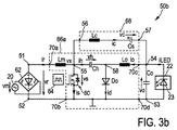
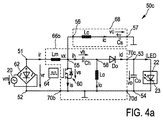
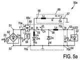
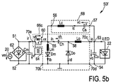
図3〜5は、本発明に係るドライバ装置の三つの基本的構成のいくつかの実施形態を示す。各構成(図3は構成1の実施形態を、図4は構成2の実施形態を、図5は構成3の実施形態を示す)は、単段式電力変換ユニット及びフィルタユニットを含む提案ドライバ装置の二つの実施形態によって示される。各提案構成に対して、フィルタコンデンサ(低周波数保持容量とも呼ぶ)Csをグランド又は負荷に接続する二つの異なる実施形態を説明する。
3-5 show several embodiments of the three basic configurations of the driver device according to the present invention. Each configuration (FIG. 3 shows an embodiment of
三つの構成は全て自己安定挙動を示し、これは、(低周波)保持容量Csの両端で所定の電圧リップルで出力電流を一定に制御することを可能にする。一実施形態においては、電力変換ユニットの昇圧インダクタLmは、非連続導通モード用に設計され、このために追加ダイオード(Dm)が昇圧インダクタに直列に結合される。また、全ての構成が高電圧負荷、例えば複数の高電圧LEDストリングに適しているが、低電圧も可能である。負荷が変わる可能性があるので、スイッチング周波数を変えることによってコンデンサ電圧を一定に制御することができる。出力電流が減少するにつれ、スイッチング周波数が上がる。したがって、各構成のタイプ1の実施形態(図3a、4a、5aの実施形態)とタイプ2の実施形態(図3b、4b、5bの実施形態)とは大部分において同等であるが、パフォーマンス、コンデンサの両端の電圧ストレス、及びスイッチに関して異なる。両タイプは似ているため、主にタイプ2の実施形態を以下に説明する。
All three configurations exhibit self-stable behavior, which allows the output current to be controlled constant with a predetermined voltage ripple across the (low frequency) holding capacitor Cs. In one embodiment, the boost inductor Lm of the power conversion unit is designed for a discontinuous conduction mode, for which an additional diode (Dm) is coupled in series with the boost inductor. Also, all configurations are suitable for high voltage loads, such as multiple high voltage LED strings, but low voltages are possible. Since the load may change, the capacitor voltage can be controlled to be constant by changing the switching frequency. As the output current decreases, the switching frequency increases. Thus, the
図6〜10に示すダイアグラムは、図3、4、及び5に示す三つの構成に関する。図6〜11は図3a、4a、5aに示す第1、第3、及び第5実施形態の低周波定常状態波形(図6、8、9)及び高周波スイッチング波形(図7、10)を示す。実施系チア50b及び50dのスイッチング波形は同等であるため、実施形態50dのスイッチング波形は別々に繰り返して示されない。全ての場合において、直列接続LEDユニットを含むLED負荷が10W定電力で動作するよう選択され、これは出力電力が一定でなければならないことを意味する。整流AC入力信号は、ヨーロッパコンセントに言及する。他の種類の負荷及び電源も使用可能である。ここに示される全ての実施形態において、最終的な力率(power factor(PF))は90%以上であり、全高調波歪(total harmonic distortion(THD))は40%未満である。
The diagrams shown in FIGS. 6-10 relate to the three configurations shown in FIGS. FIGS. 6-11 show the low frequency steady state waveforms (FIGS. 6, 8, 9) and the high frequency switching waveforms (FIGS. 7, 10) of the first, third, and fifth embodiments shown in FIGS. 3a, 4a, 5a. . Since the switching waveforms of the working
デューティサイクルはスイッチ動作に言及することに留意されたい。例えば、100%デューティサイクルは、スイッチング要素60が常にオン(閉)であることを示す。切り替えられたノードの電圧は、vxで表される。
Note that duty cycle refers to switch operation. For example, a 100% duty cycle indicates that the switching
図3aは、本発明に係るドライバ装置50aの第1実施形態を概略的に示す。ドライバ装置50aは、整流器62によって整流される、外部電源20(例えば電源電圧vmを供給するコンセント電圧電源)からの整流電源電圧vrを受ける電源入力端子51、52を備える。ドライバ装置50aは、負荷22を駆動するための駆動電圧vo及び/又は電流ioを供給するための電力出力端子53、54をさらに備える。この文脈において、本実施形態における電流ioは負荷22を流れる電流であることに留意されたい(以下で説明される、図4a、5aに示す実施形態でも同様)。これは全ての実施形態には当てはまらない。
FIG. 3a schematically shows a first embodiment of a
また、ドライバ装置50aは、単段式電力変換ユニット66aを有し、当該ユニットの入力端子70a、70bは電力入力端子51、52に結合され、出力端子70c、70dは電力出力端子53、54に結合される。電力変換ユニット66aは一つのスイッチング要素60とエネルギー保持要素Ch、具体的には一つのコンデンサを有し、両方ともにスイッチノード55に結合される。
The
また、ドライバ装置50aはフィルタインダクタLcとフィルタコンデンサCsとを有するフィルタユニット68を有する。フィルタユニット68の(フィルタインダクタLcに接続される)高電圧端子56はスイッチノード55に結合され、一方、フィルタユニット68の(フィルタコンデンサCsに接続される)低電圧端子57は、グランドに結合されている。
The
スイッチング要素60を制御するために、制御ユニット64(例えば、適切に設計又はプログラムされたコントローラ、プロセッサ、又はコンピュータ)が提供される。
In order to control the switching
該当する実施形態においては、高周波バイパス(デカップリング)のために、電力入力端子51、52の間に結合される(任意の)入力バイパスコンデンサCm(図5参照(図3及び4には示されていない))と、電力出力端子53、54の間に結合される(任意の)出力バイパスコンデンサCoが追加される。低電力入力端子52及び高電力出力端子53はともにグランドに結合される。
In the relevant embodiment, an (optional) input bypass capacitor Cm (see FIG. 5 (shown in FIGS. 3 and 4) coupled between
CuK型電力変換ユニット66aは、高電力入力端子51とスイッチノード55との間に結合された第1インダクタLmを有する。エネルギー保持要素Ch、具体的には中間コンデンサは、スイッチノード55と中間ノード58との間に結合される。第2インダクタLoは、中間ノード58と第1電力出力端子54との間に結合される。最後に、ダイオードDoが中間ノード58と低電力出力端子54との間に結合される。スイッチング要素60は、スイッチノード55と低電力入力端子52との間に結合される。
CuK type
図3bは、本発明に係るドライバ装置50bの第2実施形態を概略的に示す。ドライバ装置50aの第1実施形態と比較すると、フィルタユニット68の低電圧端子57はグランドではなく低電力出力端子54に結合される。他の要素及び結合部はドライバ装置50aの第1実施形態と同様である。
FIG. 3b schematically shows a second embodiment of the driver device 50b according to the present invention. Compared to the first embodiment of the
したがって、ドライバ装置50a、50bの第1及び第2実施形態においては、回路はCuk型電力コンバータを、直列接続された高周波フィルタインダクタLcと低周波(コンセント周波数)保持容量Csとを含み、スイッチノード55と負荷との間(第2実施形態の場合)、又はスイッチノード55とグランドとの間(第1実施形態の場合)に接続される、ローパスフィルタと組み合わせる。パフォーマンス(性能)並びにコンデンサ及びスイッチの両端でのストレス電圧は、両実施形態で関連し得る。
Therefore, in the first and second embodiments of the
また、第2実施形態の場合、出力インダクタ電流ioは出力負荷電流及び保持容量電流の両方を運ぶ。スイッチ要素60の両端の最大ストレス電圧はコンデンサChの両端の電圧であり、Vo/dである(dはデューティサイクル)。通常、保持容量電圧vcはコンセント整流器電圧vr及び出力負荷電圧voより高い。
In the second embodiment, the output inductor current io carries both the output load current and the storage capacitor current. The maximum stress voltage across the
図6に示すように、平均入力電流ir(av)は、整流コンセント電圧vrのゼロ交差にてゼロになる。デューティサイクルdは出力負荷電圧voに比例し、保持容量電圧vcに反比例する。図7は、電源(コンセント)サイクル電圧のゼロ交差から3ms後の高スイッチング周波波形を示す。図7は、入力電流irの不連続導通動作モードを示す。スイッチ60がオフの間は常にダイオード電流idが存在するため、出力での連続導通モードが保証される。ただし、これは必須ではなく、出力での非連続導通モードが許容されてもよい。
As shown in FIG. 6, the average input current ir (av) becomes zero at the zero crossing of the rectified outlet voltage vr. The duty cycle d is proportional to the output load voltage vo and inversely proportional to the storage capacitor voltage vc. FIG. 7 shows a high switching frequency waveform 3 ms after the zero crossing of the power supply (outlet) cycle voltage. FIG. 7 shows the discontinuous conduction operation mode of the input current ir. Since the diode current id is always present while the
この例において、保持容量Csは1μF(100nF/W)程度に低くてもよく、一方、一定な出力電力及び高力率が保証される。ステップダウン変換により、負荷電圧voを電源ピーク電圧(例えば、USコンセント電源の場合は70V)より著しく低くすることができる。Cukコンバータのローパスフィルタは良好な高周波フィルタリングを提供し、負荷22における低電流リップルを維持する。
In this example, the holding capacitor Cs may be as low as 1 μF (100 nF / W), while ensuring a constant output power and high power factor. By step-down conversion, the load voltage vo can be made significantly lower than the power supply peak voltage (for example, 70 V in the case of US outlet power supply). The low-pass filter of the Cuk converter provides good high frequency filtering and maintains low current ripple at the
図6に例示される定常状態波形、及び図7に例示される電源サイクルから位相角0.18πにおける高周波波形において(両図ともにドライバ装置50bの第2実施形態の場合を示す)、vm=120Veff、60Hz、スイッチング周波数200kHz、Lm=400μH、Lc=Lo=2mH、Po=10W、vo=70V、Cs=1μF、PF=95%、THD=23%、スイッチ両端の最大電圧ストレス=337Vである。「av」は、スイッチングサイクルにかけての平均成分を示し、「d」はデューティサイクルを示す。
In a steady state waveform illustrated in FIG. 6 and a high-frequency waveform at a phase angle of 0.18π from the power cycle illustrated in FIG. 7 (both diagrams show the case of the second embodiment of the driver device 50b), vm = 120Veff 60 Hz, switching
図4a及び4bは本発明に係るドライバ装置50c、50dの第3及び第4実施形態を概略的に示す。これらの実施形態はドライバ装置50a、50bと実質的に同一であるが、これらの実施形態では、Cuk型電力変換ユニット65aがSEPIC型電力変換ユニット65bに置き換えられている。また、電力出力端子53、54及び負荷22の極性が逆転されている。
4a and 4b schematically show third and fourth embodiments of
SEPIC型電力変換ユニット65bは、高電力入力端子51とスイッチノード55との間に結合された第1インダクタLmを有する。エネルギー保持要素Ch、具体的には中間コンデンサは、スイッチノード55と中間ノード58との間に結合される。ダイオードDoが中間ノード58と高電力出力端子53との間に結合される。最後に、第2インダクタLoが中間ノード58と低電力入力端子52との間に結合される。スイッチング要素60は、スイッチノード55と低電力入力端子52との間に結合される。
The SEPIC type power conversion unit 65 b has a first inductor Lm coupled between the high
したがって、ドライバ装置50c、50dの第3及び第4実施形態においては、回路はSEPIC型電力コンバータを、直列接続された高周波フィルタインダクタLcと低周波(コンセント周波数)保持容量Csとを含み、スイッチノード55と負荷との間(第4実施形態の場合)、又はスイッチノード55とグランドとの間(第3実施形態の場合)に接続される、ローパスフィルタと組み合わせる。パフォーマンス、並びにコンデンサ両端及びスイッチ両端のストレス電圧は両実施形態間で関連し得る。また、第4実施形態の場合において、出力インダクタ電流ioは、平均で出力負荷電流idマイナス保持容量電流ihを運ぶ。スイッチ60両端の最大ストレス電圧は、コンデンサCh両端の電圧vhプラス出力電圧voに等しい。通常、保持容量電圧vhは出力電圧voより高く、実質的にピーク電圧の30%より大きく振動できる。
Therefore, in the third and fourth embodiments of the
図8に示すように、平均入力電流ir(av)は、整流コンセント電圧vrのゼロ交差においてゼロになる。デューティサイクルdは出力負荷電圧voに比例し、保持容量電圧vhプラス出力負荷電圧voの2倍に反比例する。高スイッチング周波数波形は図に示す第2実施形態のものと同等である。 As shown in FIG. 8, the average input current ir (av) becomes zero at the zero crossing of the rectified outlet voltage vr. The duty cycle d is proportional to the output load voltage vo, and inversely proportional to the holding capacity voltage vh plus twice the output load voltage vo. The high switching frequency waveform is equivalent to that of the second embodiment shown in the figure.
この例において、保持容量Chは4μF程度に低くでもよく、一定な出力電力及び高力率を保証する。ステップダウン変換により、負荷電圧voは電源ピーク電圧(例えば、USコンセント電源の場合30V)より著しく低くなり得る。 In this example, the holding capacitor Ch may be as low as 4 μF, guaranteeing constant output power and high power factor. Due to the step-down conversion, the load voltage vo can be significantly lower than the power supply peak voltage (eg, 30V for US outlet power).
図8に例示の定常状態波形(ドライバ装置50dの第4実施形態に対応)において、vm=120Veff、60Hz、スイッチング周波数200kHz、Lm=300μH、Lc=Lo=2mH、Po=10W、vo=30V、Cs=4μF、PF=92%、THD=35%、スイッチ間の最大電圧ストレス=228Vである。
In the steady state waveform illustrated in FIG. 8 (corresponding to the fourth embodiment of the
図5a及び5bは、本発明に係るドライバ装置50e、50fの第5および第6実施形態を概略的に示す。これらの実施形態はドライバ装置50c、50dの実施形態と実質的に同一であるが、これらの実施形態ではSEPIC型電力変換ユニット65bがZeta型電力変換ユニット65cによって置き換えられている。また、コンデンサCs及びChの極性が逆転されている。
FIGS. 5a and 5b schematically show fifth and sixth embodiments of
Zeta型電力変換ユニット65cは、高電力入力端子51とスイッチノード55との間に結合されたスイッチング要素60を有する。第1インダクタLmがスイッチノード55と低電力入力端子52との間に結合されている。第1ダイオードDmが第1インダクタLmと直列に結合されている。エネルギー保持要素Ch、具体的には中間コンデンサは、スイッチノード55と中間ノード58との間に結合されている。第2インダクタLoが中間ノード58と高電力出力端子53との間に結合されている。最後に、第2ダイオードDoが中間ノード58と低電力出力端子54との間に結合されている。
Zeta type power conversion unit 65 c has a switching
よって、ドライバ装置50e、50fの第5および第6実施形態において、回路はZeta型の電力コンバータを、直列接続された高周波フィルタインダクタLcと低周波(コンセント周波数)保持容量Csとを有し、スイッチノード55と負荷との間(第6実施形態の場合)、又はスイッチノード55とグランドとの間(第5実施形態の場合)に接続される、ローパスフィルタを組み合わせる。パフォーマンス並びにコンデンサ両端及びスイッチ両端のストレス電圧における違いは両実施形態間で関連し得る。また、第6実施形態の場合、出力インダクタ電流ioは出力負荷電流id及び保持容量電流ihの両方を運ぶ。スイッチ60両端の最大ストレス電圧はコンデンサCh両端の電圧vhプラス整流コンセント電圧vrに等しい。通常、保持容量電圧vhはコンセント整流電圧vr及び出力負荷電圧voより高い。
Therefore, in the fifth and sixth embodiments of the
図9に示すように、この実施形態においては(他の構成と異なり)、平均入力電流ir(av)は整流コンセント電圧vrのゼロ交差においてゼロにならない。デューティサイクルdは出力負荷電圧voに比例し、整流コンセント電圧vrマイナス保持容量電圧vhに反比例する。 As shown in FIG. 9, in this embodiment (unlike other configurations), the average input current ir (av) does not become zero at the zero crossing of the rectified outlet voltage vr. The duty cycle d is proportional to the output load voltage vo and inversely proportional to the rectified outlet voltage vr minus the holding capacity voltage vh.
図10は、電源(コンセント)サイクル電圧のゼロ交差から3ms後の高スイッチング周波数波形を示す。図10は、昇圧インダクタLmの非連続動作モードを示す。スイッチ60がオフの間はダイオード電流idが常に存在するため、出力では連続導通モードが保証される。ただし、これは必須ではなく、出力での非連続導通モードが許容され得る。
FIG. 10 shows a high switching frequency waveform 3 ms after the zero crossing of the power supply (outlet) cycle voltage. FIG. 10 shows the discontinuous operation mode of the boost inductor Lm. Since the diode current id is always present while the
この例において、保持容量は2μF(200nF/W)程度に低くてもよく、それても一定な出力電力及び高力率を保証する。ステップダウン変換により、負荷電圧voは電源ピーク電圧(例えば、USコンセント電源の場合は100V)より著しく低くなり得る。Zeta型段階のローパスフィルタは良好な高周波フィルタリングを提供し、LED負荷における低電流リップルを維持する。いくつかの動作条件においては整流入力電流irが負になり得るため、好ましくは、入力にて高周波デカップリング(バイパス)コンデンサCmが用いられる。 In this example, the holding capacitance may be as low as 2 μF (200 nF / W), yet guarantees a constant output power and high power factor. Due to the step-down conversion, the load voltage vo can be significantly lower than the power supply peak voltage (eg, 100V for US outlet power). The Zeta type stage low pass filter provides good high frequency filtering and maintains low current ripple in the LED load. Since the rectified input current ir can be negative under some operating conditions, a high frequency decoupling (bypass) capacitor Cm is preferably used at the input.
図9に示す定常状態波形、及び図10に示す電源(コンセント)サイクルから位相角0.18πの高周波波形(ともにドライバ装置50fの第6実施形態の場合)において、vm=120Veff、60Hz、スイッチング周波数200kHz、Lm=400μH、Lc=Lo=4mH、Po=10W、vo=100V、Cs=2μF、PF=94%、THD=36%、スイッチ間最大電圧ストレス=398Vである。
In the steady-state waveform shown in FIG. 9 and the high-frequency waveform having a phase angle of 0.18π from the power supply (outlet) cycle shown in FIG. 10 (both in the case of the sixth embodiment of the driver device 50f), vm = 120 Veff, 60 Hz, switching
次に、本発明に係る制御方法及び制御装置が説明される。図11は、制御ユニット64’の第1実施形態を含むドライバ装置50gの他の実施形態を示す(ドライバ装置の他の部品は単一のブロック50’で概略的に示す)。LED電流iLEDが比較要素64aにおいて測定され、(プリセット又は可変の)基準電流iLED_refと比較される。制御誤差err_iはコントローラブロック64b(PI)内で処理され、操作変数としてのデューティサイクルdとなる。(ゲート)ドライバブロック64cにおいて、プリセットスイッチング周波数fsと合わせて、スイッチング要素60の制御信号S60を表すゲート駆動信号が形成される。
Next, a control method and a control apparatus according to the present invention will be described. FIG. 11 shows another embodiment of the
図12は、スイッチング要素60(のゲートの)タイミングダイアグラムを示す。 FIG. 12 shows a timing diagram of the switching element 60 (of the gate).
典型的には降圧コンバータで行われるように、デューティサイクルは基本的には制御誤差に関連付けられる。ドライバ装置50gの実施形態に関しては、正の制御誤差err_i(小さすぎる電流)はdの増加を引き起こし、その逆も同様である。
As typically done in a buck converter, the duty cycle is basically related to the control error. For the embodiment of the
自己安定挙動は、Cs両端の電圧ストレスの限界を超えることなく適切な電力バランスを保証する。これは提案の回路配置及び採用の制御スキームによって得られる。例えば、出力から取り出される平均電力より入力から引き込まれる平均電力が大きい場合、バス電圧vcが高くなり、dが減少するように制御され、入力電力が減らされる。他の実施形態も同様に動作可能である。ドライバ装置50a、50c、50eの実施形態に対して、ドライバ装置50b、50d、50fの実施形態ではデューティサイクルの意味が切り替えらえる、すなわち、dが1−dに置き換えられる。バス電圧及びコンセント電流(PF)等の他の動作特性は、通常明確には制御されない。これらの特性は、設計及び動作選択及び許容範囲による。
Self-stabilizing behavior ensures proper power balance without exceeding the voltage stress limits across Cs. This is obtained by the proposed circuit arrangement and adopted control scheme. For example, when the average power drawn from the input is larger than the average power drawn from the output, the bus voltage vc is increased and d is controlled to decrease, and the input power is reduced. Other embodiments can operate similarly. Compared with the embodiments of the
他の実施形態においては、最大バス電圧も上記制御によって明確に制御され、特に、スイッチング周波数も操作することによって明確に制御される。出力電流を制御するためにdを操作する一方、バス電圧の増加(例えば、高コンセント電圧又は高出力電圧に由来する)に対応してfsが上昇される。代わりに、T_on及びT_offを別々に制御してもよいが、この場合もスイッチングパターンは同様になる。 In other embodiments, the maximum bus voltage is also explicitly controlled by the above control, in particular, it is also explicitly controlled by manipulating the switching frequency. While d is manipulated to control the output current, fs is raised in response to an increase in bus voltage (eg, derived from a high outlet voltage or a high output voltage). Alternatively, T_on and T_off may be controlled separately, but in this case, the switching pattern is the same.
基準信号iLED_refが可変で定格最大値よりはるかに低い場合、バス電圧が過度に高くなるのを防ぐため(すなわち、過度の昇圧を防ぐため)、他の実施形態においては上記制御はバーストモードに入る、すなわち、fsより低い(例えば、10〜1000分の1)バースト頻度にてコンバータのスイッチをオフにする。PFを改善するために、又は所定の種類の壁コンセントディマーへの適合を高めるために、バス電圧制御のための周波数変調に加えて、又はその代わりに、入力電流の変調にfsを用いてもよい。 If the reference signal iLED_ref is variable and much lower than the rated maximum, to prevent the bus voltage from becoming too high (ie to prevent excessive boosting), in other embodiments the control enters burst mode. That is, the converter is switched off at a burst frequency lower than fs (for example, 10 to 1000 times). In addition to or instead of frequency modulation for bus voltage control, fs may be used to modulate the input current in order to improve PF or to enhance the fit to a given type of wall outlet dimmer. Good.
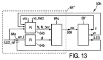
図13は、制御ユニット64”の第2実施形態を含むドライバ装置50hの他の実施形態を示す。図11の実施形態に対して、制御ユニット64”は、さらに第2コントローラブロック64d(PI)を有し、操作変数としてのスイッチング周波数fs、fs_brstが(ゲート)ドライバブロック64cに供給される。第2コントローラブロック64dは、入力基準電流iLED_refとしてバス電圧vc、入力電流ir、入力電圧vm、及び最大バス電圧vc_maxを受ける。
FIG. 13 shows another embodiment of the
本発明によれば、前処理ユニットが組み込まれ、且つ、高力率を備える一方で負荷に一定な出力電流を供給する単段式電力コンバータトポロジーを備えるドライバ装置が提案される。少数の部品しか必要なく、ハーフ/フルスイッチブリッジや大きな電界コンデンサは必要ない。これは、ローパスフィルタが一体化された(組み込まれた)電力コンバータを適切に制御することで達成される。上記変換機能の実行には、通常一つのスイッチ(例えば、MOSFETトランジスタ)しか要求されない。ドライバ装置は、高電圧LEDストリングを使用するオフラインLEDドライバに好適に適用可能である。 In accordance with the present invention, a driver device is proposed that incorporates a preprocessing unit and has a single stage power converter topology that provides a constant output current to the load while having a high power factor. Only a few components are needed, and half / full switch bridges and large field capacitors are not needed. This is achieved by appropriately controlling a power converter with an integrated (incorporated) low pass filter. Only one switch (eg, a MOSFET transistor) is normally required to perform the conversion function. The driver device can be suitably applied to an off-line LED driver using a high voltage LED string.
本発明の実施形態によれば、一つの昇圧インダクタが非連続導通モードで動作する。これを強化するために、ダイオードが好適に直列に結合される(入力整流器ブリッジのものか、又は専用のもの)。高スイッチング周波数電流成分をフィルタリング除去するために、好ましくは二つのインダクタが用いられる。好ましくは、一つの高周波バイパスコンデンサが出力に結合され、またいくつかの場合においては、二つ目が入力(整流ブリッジの出力)に結合される。 According to an embodiment of the present invention, one boost inductor operates in a discontinuous conduction mode. To enhance this, diodes are preferably coupled in series (either from the input rectifier bridge or dedicated). Two inductors are preferably used to filter out the high switching frequency current components. Preferably, one high frequency bypass capacitor is coupled to the output, and in some cases the second is coupled to the input (the output of the rectifier bridge).
スイッチノードは、さらに第3インダクタ、具体的には高周波インダクタに接続され、高周波インダクタは、小さな低周波保持容量に直列接続されることによってフィルタを形成する。スイッチノードはさらに中間保持要素として用いられる高周波コンデンサに接続され、スイッチングサイクル内で出力にエネルギーを運ぶ。整流器コンセントは昇圧インダクタ又はスイッチのいずれかに接続されてもよい。 The switch node is further connected to a third inductor, specifically a high frequency inductor, and the high frequency inductor forms a filter by being connected in series to a small low frequency holding capacitor. The switch node is further connected to a high frequency capacitor used as an intermediate holding element and carries energy to the output within the switching cycle. The rectifier outlet may be connected to either a boost inductor or a switch.
低周波保持容量の一方の端子はグランド又は負荷のいずれに結合されてもよい。また、負荷(例えばLED)電流のみが一定に制御されてもよいし(例えば、デューティサイクルによって)、周波数を操作するとともにLED電流及びバス電圧の両方を二つのループで制御してもよい。 One terminal of the low frequency holding capacitor may be coupled to either ground or a load. Also, only the load (eg, LED) current may be controlled to be constant (eg, by duty cycle) or the frequency may be manipulated and both the LED current and bus voltage may be controlled in two loops.
本発明は、コンシューマー(消費者)用及び「プロシューマ―(生産消費者)」用ドライバに適用され、例えば2W以上で、照明装置に組み込まれて使用されたり、又はHV LED用の外部LEDドライバ等に適用される。他の適用例は、THD要求(例えば、20%)及びHV LEDストリング負荷が緩和された非コンセント独立プロフェッショナル(又は生産者用)ドライバである。 The present invention is applied to a consumer (consumer) driver and a "prosumer (production consumer)" driver. For example, an external LED driver for HV LED or the like that is incorporated in a lighting device at 2 W or more. Applies to Other applications are non-outlet independent professional (or producer) drivers with reduced THD requirements (eg, 20%) and HV LED string load.
以上、本発明を記載及び図面によって詳細に記述及び描写してきたが、記述及び描写はあくまで説明のためであって限定をするものではない。本発明は、開示された実施形態に限定されない。図面、明細書、及び特許請求の範囲を参照することで、当業者は、発明を実施するにあたり、開示された実施形態の他の変形例を理解及び実行できるであろう。 Although the present invention has been described and illustrated in detail with reference to the drawings and the drawings, the description and the description are only for the purpose of explanation and are not intended to be limiting. The invention is not limited to the disclosed embodiments. With reference to the drawings, the specification, and the claims, those skilled in the art will understand and implement other variations of the disclosed embodiments in carrying out the invention.
特許請求の範囲において、「有する(又は備える、含む)」という単語は他の要素又はステップを除外せず、要素は複数を除外しない。一つの要素又は他のユニットが請求項に記載の複数の項目の機能を満たしてもよい。いくつかの手段が異なる独立請求項に記載されているからといって、これらの手段の組み合わせを好適に用いることができないとは限らない。 In the claims, the word “comprising” does not exclude other elements or steps, and an element does not exclude a plurality. One element or other unit may fulfill the functions of several items recited in the claims. The mere fact that certain measures are recited in different independent claims does not necessarily indicate that a combination of these measures cannot be used to advantage.
請求項内の参照符号は特許請求の範囲を限定しない。
Reference numerals in the claims do not limit their scope.
Claims (12)
第1電力入力端子及び第2電力入力端子を含み、外部電源から整流電源電圧を受ける電力入力端子と、
前記第1電力入力端子及び前記第2電力入力端子のいずれとも直接接続されていない第1電力出力端子及び第2電力出力端子を含み、負荷を駆動するための駆動電圧及び/又は電流を供給する電力出力端子と、
いずれもスイッチノードに結合された単一のスイッチング要素及びエネルギー保持要素を含む、前記電力入力端子に結合された単段式電力変換ユニットであって、前記電力出力端子は単段式電力変換ユニットの出力部によって表される、前記単段式電力変換ユニットと、
前記スイッチノードと前記第1電力入力端子及び前記第2電力入力端子のいずれか一方との間に結合された第1インダクタと、
前記スイッチノードと前記第1電力出力端子との間に結合された、フィルタインダクタ及びフィルタコンデンサを含むフィルタユニットと、
前記スイッチング要素を制御する制御ユニットと
を有し、
前記エネルギー保持要素は、前記スイッチノードと中間ノードとの間に結合され、
前記中間ノードと前記第1電力出力端子及び前記第2電力出力端子のいずれか一方との間に第2インダクタが結合され、
前記中間ノードと前記第1電力出力端子及び前記第2電力出力端子のいずれか他方との間にダイオードが結合される、
ドライバ装置。 A driver device for a load,
A power input terminal including a first power input terminal and a second power input terminal and receiving a rectified power supply voltage from an external power supply;
Including a first power output terminal and a second power output terminal that are not directly connected to either the first power input terminal or the second power input terminal, and supplies a drive voltage and / or current for driving a load A power output terminal;
A single stage power conversion unit coupled to the power input terminal, both including a single switching element and an energy holding element coupled to a switch node, wherein the power output terminal of the single stage power conversion unit Represented by the output unit, the single-stage power conversion unit;
A first inductor coupled between the switch node and one of the first power input terminal and the second power input terminal ;
A filter unit including a filter inductor and a filter capacitor coupled between the switch node and the first power output terminal ;
A control unit for controlling the switching element,
The energy holding element is coupled between the switch node and an intermediate node;
A second inductor is coupled between the intermediate node and one of the first power output terminal and the second power output terminal ;
A diode is coupled between the intermediate node and one of the first power output terminal and the second power output terminal ;
Driver device.
前記スイッチング要素は、前記スイッチノードと前記第2電力出力端子との間に結合され、
前記第2インダクタは、前記中間ノードと前記第1電力出力端子との間に結合され、
前記ダイオードは、前記中間ノードと前記第2電力出力端子との間に結合される、請求項1に記載のドライバ装置。 The single-stage power conversion unit includes a Cuk type converter,
The switching element is coupled between the switch node and the second power output terminal;
The second inductor is coupled between the intermediate node and the first power output terminal,
Said diode, said coupled between the intermediate node and the second power output terminal, the driver device according to claim 1.
前記スイッチング要素は、前記スイッチノードと前記第2電力出力端子との間に結合され、
前記第2インダクタは、前記中間ノードと前記第2電力出力端子との間に結合され、
前記ダイオードは、前記中間ノードと前記第1電力出力端子との間に結合される、請求項1に記載のドライバ装置。 The single-stage power conversion unit includes a SEPIC type converter,
The switching element is coupled between the switch node and the second power output terminal;
The second inductor is coupled between the intermediate node and the second power output terminal,
Said diode, said coupled between the intermediate node and the first power output terminal, the driver device according to claim 1.
前記スイッチング要素は、前記第1電力入力端子と前記スイッチノードとの間に結合され、
前記第1インダクタに直列に他のダイオードが結合され、
前記第2インダクタは、前記中間ノードと前記第1電力出力端子との間に結合され、
前記ダイオードは、前記中間ノードと前記第2電力出力端子との間に結合される、請求項1に記載のドライバ装置。 The single-stage power conversion unit includes a Zeta type converter,
It said switching element is coupled between said first power input terminal and the switch node,
Another diode is coupled in series with the first inductor;
The second inductor is coupled between the intermediate node and the first power output terminal,
Before Kida diode, said coupled between the intermediate node and the second power output terminal, the driver device according to claim 1.
前記照明アセンブリを駆動する、請求項1乃至11の何れか一項に記載のドライバ装置と
を有する、照明装置。 And illumination assemblies comprising one or more lighting units,
Driving the illumination assembly, and a driver device according to any one of claims 1 to 11, the lighting device.
Applications Claiming Priority (3)
| Application Number | Priority Date | Filing Date | Title |
|---|---|---|---|
| EP11170268.4 | 2011-06-17 | ||
| EP11170268 | 2011-06-17 | ||
| PCT/IB2012/052936 WO2012172472A1 (en) | 2011-06-17 | 2012-06-11 | Single switch driver device having lc filter, for driving a load, in particular an led unit |
Publications (3)
| Publication Number | Publication Date |
|---|---|
| JP2014520366A JP2014520366A (en) | 2014-08-21 |
| JP2014520366A5 JP2014520366A5 (en) | 2015-07-30 |
| JP6133280B2 true JP6133280B2 (en) | 2017-05-24 |
Family
ID=46458569
Family Applications (1)
| Application Number | Title | Priority Date | Filing Date |
|---|---|---|---|
| JP2014515319A Active JP6133280B2 (en) | 2011-06-17 | 2012-06-11 | Single switch driver device with LC filter for driving load, especially LED unit |
Country Status (5)
| Country | Link |
|---|---|
| US (1) | US9210749B2 (en) |
| EP (1) | EP2721906B1 (en) |
| JP (1) | JP6133280B2 (en) |
| CN (1) | CN103609198B (en) |
| WO (1) | WO2012172472A1 (en) |
Families Citing this family (19)
| Publication number | Priority date | Publication date | Assignee | Title |
|---|---|---|---|---|
| DE102010041632A1 (en) * | 2010-09-29 | 2012-03-29 | Osram Gesellschaft mit beschränkter Haftung | Circuit arrangement for operating at least two semiconductor light sources |
| JP6127290B2 (en) * | 2013-05-28 | 2017-05-17 | 国立研究開発法人宇宙航空研究開発機構 | Charger / discharger with equalization function using both converter and multi-stage voltage doubler rectifier circuit |
| CN106465502B (en) | 2014-05-30 | 2018-10-12 | 飞利浦照明控股有限公司 | Driver for driving load |
| JP6429148B2 (en) | 2014-11-20 | 2018-11-28 | パナソニックIpマネジメント株式会社 | Lighting device and lighting apparatus using the same |
| JP6270698B2 (en) * | 2014-11-26 | 2018-01-31 | 新電元工業株式会社 | LED driver device |
| US9723667B1 (en) * | 2015-04-09 | 2017-08-01 | Universal Lighting Technologies, Inc. | Output tuning and dimming interface for an LED driver |
| US9693411B1 (en) * | 2015-04-09 | 2017-06-27 | Universal Lighting Technologies, Inc. | LED driver configuration and dimming interface for dynamic adjustment of driver operating parameters |
| DE102015210710A1 (en) * | 2015-06-11 | 2016-12-15 | Tridonic Gmbh & Co Kg | Clocked flyback converter circuit |
| FR3040839B1 (en) * | 2015-09-04 | 2019-10-25 | Commissariat A L'energie Atomique Et Aux Energies Alternatives | ELECTRONIC CONVERTER AND LIGHTING SYSTEM COMPRISING SUCH A CONVERTER |
| US9769896B1 (en) | 2015-12-04 | 2017-09-19 | Universal Lighting Technologies, Inc. | LED driver with offline tuning interface using hot and neutral inputs |
| CN105792421B (en) * | 2016-04-05 | 2017-08-08 | 江南大学 | A kind of no bridge type LED drive power |
| CN106413202B (en) * | 2016-11-25 | 2018-03-16 | 哈尔滨工业大学 | Primary-side-control LED drive circuit based on SEPIC Yu Flyback circuits |
| US10264641B1 (en) | 2017-07-05 | 2019-04-16 | Universal Lighting Technologies, Inc. | Lighting system and method for dynamically regulating driven current to an analog or digital dimming interface |
| US10588205B1 (en) | 2018-01-26 | 2020-03-10 | Universal Lighting Technologies, Inc. | Isolated digital control device for LED driver using NFC technology |
| US10595383B1 (en) | 2018-01-26 | 2020-03-17 | Universal Lighting Technologies, Inc. | Device and method for programming or configuring of NFC equipped LED driver |
| US10560993B1 (en) | 2018-03-08 | 2020-02-11 | Universal Lighting Technologies, Inc. | Dimming controller for LED driver and method of indirect power estimation |
| WO2020149870A1 (en) * | 2018-12-28 | 2020-07-23 | Huawei Technologies Co., Ltd. | Hybrid power converter and method |
| TWI699969B (en) * | 2019-10-24 | 2020-07-21 | 瑞昱半導體股份有限公司 | Filter and operation method |
| CN114205954A (en) * | 2021-12-30 | 2022-03-18 | 福州大学 | Electrolytic-capacitor-free control method for improved Sepic-LED driving circuit |
Family Cites Families (14)
| Publication number | Priority date | Publication date | Assignee | Title |
|---|---|---|---|---|
| JPH0832160B2 (en) * | 1990-01-31 | 1996-03-27 | 三菱電機株式会社 | Pulse power supply |
| JPH05176532A (en) * | 1991-09-25 | 1993-07-13 | Yamaha Corp | Power circuit |
| US5442539A (en) * | 1992-10-02 | 1995-08-15 | California Institute Of Technology | CuK DC-to-DC switching converter with input current shaping for unity power factor operation |
| US5442534A (en) | 1993-02-23 | 1995-08-15 | California Institute Of Technology | Isolated multiple output Cuk converter with primary input voltage regulation feedback loop decoupled from secondary load regulation loops |
| US20030066555A1 (en) | 2000-12-04 | 2003-04-10 | Hui Ron Shu Yuen | Maximum power tracking technique for solar panels |
| KR100497393B1 (en) * | 2003-06-20 | 2005-06-23 | 삼성전자주식회사 | Apparatus for improving power factor of power supply in a plasma display panel driving system and design method thereof |
| US7847783B2 (en) * | 2005-10-11 | 2010-12-07 | O2Micro International Limited | Controller circuitry for light emitting diodes |
| US7889519B2 (en) * | 2006-01-12 | 2011-02-15 | Massachusetts Institute Of Technology | Methods and apparatus for a resonant converter |
| JP5169039B2 (en) * | 2007-06-29 | 2013-03-27 | Nec東芝スペースシステム株式会社 | DC-DC converter |
| JP2009089564A (en) * | 2007-10-03 | 2009-04-23 | Nec Toshiba Space Systems Ltd | Dc/dc converter |
| EP2299569B1 (en) * | 2009-09-21 | 2014-07-16 | BIONIC Engineering 5D+ AG | Direct current converter and direct current conversion method |
| JP5759668B2 (en) * | 2009-10-02 | 2015-08-05 | Fdk株式会社 | Multi-series LED drive circuit |
| CN101867289B (en) | 2010-05-19 | 2012-05-30 | 杭州矽力杰半导体技术有限公司 | Switch power supply with constant voltage/constant current output and control method thereof |
| TWI454041B (en) * | 2011-12-06 | 2014-09-21 | Champion Elite Co Ltd | Piezoelectric resonant light emitting diode driving circuit |
-
2012
- 2012-06-11 EP EP12732709.6A patent/EP2721906B1/en active Active
- 2012-06-11 CN CN201280029663.5A patent/CN103609198B/en active Active
- 2012-06-11 US US14/125,787 patent/US9210749B2/en active Active
- 2012-06-11 WO PCT/IB2012/052936 patent/WO2012172472A1/en active Application Filing
- 2012-06-11 JP JP2014515319A patent/JP6133280B2/en active Active
Also Published As
| Publication number | Publication date |
|---|---|
| EP2721906A1 (en) | 2014-04-23 |
| WO2012172472A1 (en) | 2012-12-20 |
| JP2014520366A (en) | 2014-08-21 |
| EP2721906B1 (en) | 2017-08-16 |
| CN103609198A (en) | 2014-02-26 |
| US9210749B2 (en) | 2015-12-08 |
| US20140117868A1 (en) | 2014-05-01 |
| CN103609198B (en) | 2016-10-19 |
Similar Documents
| Publication | Publication Date | Title |
|---|---|---|
| JP6133280B2 (en) | Single switch driver device with LC filter for driving load, especially LED unit | |
| JP6118316B2 (en) | DC-DC driver device with input and output filters for driving a load, in particular an LED unit | |
| US9497814B2 (en) | Driver device and driving method for driving a load, in particular an LED unit | |
| CN104902613B (en) | Mixing dimming control technique for LED driver | |
| JP5981337B2 (en) | Low cost power supply circuit and method | |
| CN202652596U (en) | Circuit for controlling dimming level of one or more light emitting diodes | |
| US9258858B2 (en) | Active capacitor circuit | |
| CN103262650A (en) | Synchronous regulation for led string driver | |
| WO2008152565A2 (en) | Supply circuit, in particular for leds | |
| WO2017045075A1 (en) | Current ripple sensing controller for a single-stage led driver | |
| Agrawal et al. | A review of different DC/DC converters for power quality improvement in LED lighting load | |
| KR20150047951A (en) | Led power supply and led lighting apparatus using the same | |
| KR101454158B1 (en) | Electrolytic Capacitor-less Power Supply for Lighting LED Drive and 120Hz Ripple Reduction Method of the Same | |
| Padmavathi et al. | A survey on efficient converter driver techniques for LED lighting applications | |
| US8519638B2 (en) | Electronic ballast for a high intesity discharge lamp | |
| JP2021529422A (en) | LED driver and LED lighting system for use with high frequency electronic ballasts | |
| JP6328394B2 (en) | Dimming lighting device | |
| JP2014082156A (en) | Lighting device | |
| KR102059635B1 (en) | Led power supply and control method thereof | |
| Balasubramanian et al. | Programmable LED drivers | |
| da Fonseca et al. | Single stage high power factor converter using coupled input boost inductor BCM without eletrolytic capacitor to drive power LED |
Legal Events
| Date | Code | Title | Description |
|---|---|---|---|
| A521 | Request for written amendment filed |
Free format text: JAPANESE INTERMEDIATE CODE: A523 Effective date: 20150609 |
|
| A621 | Written request for application examination |
Free format text: JAPANESE INTERMEDIATE CODE: A621 Effective date: 20150609 |
|
| A977 | Report on retrieval |
Free format text: JAPANESE INTERMEDIATE CODE: A971007 Effective date: 20160720 |
|
| A131 | Notification of reasons for refusal |
Free format text: JAPANESE INTERMEDIATE CODE: A131 Effective date: 20160816 |
|
| A711 | Notification of change in applicant |
Free format text: JAPANESE INTERMEDIATE CODE: A711 Effective date: 20160927 |
|
| A521 | Request for written amendment filed |
Free format text: JAPANESE INTERMEDIATE CODE: A523 Effective date: 20161110 |
|
| TRDD | Decision of grant or rejection written | ||
| A01 | Written decision to grant a patent or to grant a registration (utility model) |
Free format text: JAPANESE INTERMEDIATE CODE: A01 Effective date: 20170321 |
|
| A61 | First payment of annual fees (during grant procedure) |
Free format text: JAPANESE INTERMEDIATE CODE: A61 Effective date: 20170419 |
|
| R150 | Certificate of patent or registration of utility model |
Ref document number: 6133280 Country of ref document: JP Free format text: JAPANESE INTERMEDIATE CODE: R150 |
|
| S531 | Written request for registration of change of domicile |
Free format text: JAPANESE INTERMEDIATE CODE: R313531 |
|
| S533 | Written request for registration of change of name |
Free format text: JAPANESE INTERMEDIATE CODE: R313533 |
|
| R350 | Written notification of registration of transfer |
Free format text: JAPANESE INTERMEDIATE CODE: R350 |
|
| R250 | Receipt of annual fees |
Free format text: JAPANESE INTERMEDIATE CODE: R250 |
|
| R250 | Receipt of annual fees |
Free format text: JAPANESE INTERMEDIATE CODE: R250 |
|
| R250 | Receipt of annual fees |
Free format text: JAPANESE INTERMEDIATE CODE: R250 |
|
| R250 | Receipt of annual fees |
Free format text: JAPANESE INTERMEDIATE CODE: R250 |