JP6124555B2 - Solid-state imaging device and distance measuring device using the same - Google Patents
Solid-state imaging device and distance measuring device using the same Download PDFInfo
- Publication number
- JP6124555B2 JP6124555B2 JP2012241700A JP2012241700A JP6124555B2 JP 6124555 B2 JP6124555 B2 JP 6124555B2 JP 2012241700 A JP2012241700 A JP 2012241700A JP 2012241700 A JP2012241700 A JP 2012241700A JP 6124555 B2 JP6124555 B2 JP 6124555B2
- Authority
- JP
- Japan
- Prior art keywords
- waveguide
- solid
- photoelectric conversion
- imaging device
- state imaging
- Prior art date
- Legal status (The legal status is an assumption and is not a legal conclusion. Google has not performed a legal analysis and makes no representation as to the accuracy of the status listed.)
- Expired - Fee Related
Links
Images


Classifications
-
- G—PHYSICS
- G02—OPTICS
- G02B—OPTICAL ELEMENTS, SYSTEMS OR APPARATUS
- G02B7/00—Mountings, adjusting means, or light-tight connections, for optical elements
- G02B7/28—Systems for automatic generation of focusing signals
-
- H—ELECTRICITY
- H04—ELECTRIC COMMUNICATION TECHNIQUE
- H04N—PICTORIAL COMMUNICATION, e.g. TELEVISION
- H04N25/00—Circuitry of solid-state image sensors [SSIS]; Control thereof
- H04N25/70—SSIS architectures; Circuits associated therewith
- H04N25/703—SSIS architectures incorporating pixels for producing signals other than image signals
- H04N25/704—Pixels specially adapted for focusing, e.g. phase difference pixel sets
Landscapes
- Physics & Mathematics (AREA)
- General Physics & Mathematics (AREA)
- Optics & Photonics (AREA)
- Engineering & Computer Science (AREA)
- Multimedia (AREA)
- Signal Processing (AREA)
- Solid State Image Pick-Up Elements (AREA)
- Focusing (AREA)
- Automatic Focus Adjustment (AREA)
- Transforming Light Signals Into Electric Signals (AREA)
Description
本発明は、固体撮像素子、その固体撮像素子を用いた測距装置、その測距装置を用いたデジタルスチルカメラやデジタルビデオカメラなどの撮像装置等に関する。 The present invention relates to a solid-state imaging device, a distance measuring device using the solid-state imaging device, an imaging device such as a digital still camera and a digital video camera using the distance measuring device, and the like.
デジタルスチルカメラやビデオカメラにおいて、AF(自動焦点調節)用距離検出技術が知られている。このようなAF用距離検出技術に関し、特許文献1では、固体撮像素子の一部の画素に測距機能を持たせ、位相差方式で検出するようにした固体撮像素子が提案されている。この位相差方式とは、結像光学系の瞳上の異なる領域を通過した光の像を比較し、ステレオ画像による三角測量を用いて被写体距離を検出する方法である。これによると、従来のコントラスト方式とは異なり、被写体距離を測定するためにレンズを動かす必要が無いため、高速高精度なAFが可能となる。また、動画撮影時にリアルタイムAFが可能になる。特許文献1では、測距画素の構造として、複数の光電変換部上に導波路を設けた固体撮像素子が開示されている。結像光学系の瞳上の異なる領域を通過した光を、導波路端面に結像面を有するマイクロレンズを用いて、異なる2つの導波路に結合させることで、異なる光電変換部に導き、距離を測定することができる。
For digital still cameras and video cameras, AF (automatic focus adjustment) distance detection technology is known. With regard to such AF distance detection technology,
しかしながら、特許文献1の固体撮像素子では、固体撮像素子の周辺部や明るい結像光学系に対する固体撮像素子において、測距画素に大きな角度で入射する光束が多くなると、測距精度が悪化することがある。測距画素に大きな角度で入射する光束は、導波路で高次の固有モードと結合し易く、導波路内に電場分布が広がった導波モードで伝播し、画素内の複数の光電変換部に到達する。そのため、各瞳領域を通過した光を異なる光電変換部に選択的に導くことが困難となり、測距精度が悪化することがある。本発明は、上記課題に鑑み、測距画素に大きな角度で入射する光束が多い条件においても、高精度な測距を行うことができ、特に画素サイズの小さい場合においても、高精度の測距が可能となる固体撮像素子に関する技術の提供を目的とする。
However, in the solid-state imaging device of
本発明の一側面の固体撮像素子は、複数の光電変換部と、該複数の光電変換部よりも光の入射側に設けられた導波路と、を有する画素を含む固体撮像素子である。そして、前記導波路は、コア部材と、前記コア部材よりも屈折率が低い媒質により形成されるクラッド部材と、を有し、前記複数の光電変換部と前記導波路の間に、前記導波路から射出された光が伝搬する、該導波路の前記コア部材よりも屈折率が低い媒質を有する層が設けられており、前記複数の光電変換部の間の領域に対応する位置に、少なくとも一部が前記層の中に含まれている散乱部が設けられており、前記散乱部は、周囲の媒質よりも屈折率が低い、光を透過する媒質からなることを特徴とする。また、本発明の他の一側面の固体撮像素子は、複数の光電変換部と、該複数の光電変換部よりも光の入射側に設けられた導波路と、を有する画素を含む固体撮像素子であって、前記導波路は、コア部材と、前記コア部材よりも屈折率が低い媒質により形成されるクラッド部材と、を有し、前記複数の光電変換部と前記導波路の間に、該導波路の前記コア部材よりも屈折率が低い媒質を有する層が設けられており、当該固体撮像素子の中央部に位置する画素よりも、当該固体撮像素子の周辺部に位置する画素の方が、前記層の厚みが厚くなっていることを特徴とする。また、本発明の他の一側面の固体撮像素子は、複数の光電変換部と、該複数の光電変換部よりも光の入射側に設けられた導波路と、を有する画素を含む固体撮像素子であって、前記導波路は、コア部材と、前記コア部材よりも屈折率が低い媒質により形成されるクラッド部材と、を有し、前記複数の光電変換部と前記導波路の間に、前記導波路から射出された光が伝搬する、該導波路の前記コア部材よりも屈折率が低い媒質を有する層が設けられており、前記複数の光電変換部の間の領域に対応する位置に、周囲の媒質よりも屈折率が低い媒質からなる散乱部が設けられており、当該固体撮像素子の中央部に位置する画素よりも、当該固体撮像素子の周辺部に位置する画素の方が、前記散乱部の大きさが大きいことを特徴とする。また、本発明の他の一側面の固体撮像素子は、複数の光電変換部と、該複数の光電変換部よりも光の入射側に設けられた導波路と、を有する画素を含む固体撮像素子であって、前記導波路は、コア部材と、前記コア部材よりも屈折率が低い媒質により形成されるクラッド部材と、を有し、前記複数の光電変換部と前記導波路の間に、前記導波路から射出された光が伝搬する、該導波路の前記コア部材よりも屈折率が低い媒質を有する層が設けられており、前記複数の光電変換部の間の領域に対応する位置に、周囲の媒質よりも屈折率が低い媒質からなる散乱部が設けられており、前記層の中において、前記光電変換部よりも外側の部分に対応する部分に光吸収部が形成されており、当該固体撮像素子の中央部に位置する画素よりも、当該固体撮像素子の周辺部に位置する画素の方が、前記光吸収部の大きさが大きいことを特徴とする。 The solid-state imaging device of one aspect of the present invention is a solid-state imaging element including pixels having a plurality of photoelectric conversion unit, and a waveguide provided on a light incident side than the plurality of photoelectric conversion unit. The waveguide includes a core member and a clad member formed of a medium having a refractive index lower than that of the core member, and the waveguide is interposed between the plurality of photoelectric conversion units and the waveguide. A layer having a medium having a refractive index lower than that of the core member of the waveguide through which light emitted from the waveguide propagates is provided , and at least one position is provided at a position corresponding to a region between the plurality of photoelectric conversion units. A scattering portion is provided in which the portion is included in the layer, and the scattering portion is made of a light transmitting medium having a refractive index lower than that of the surrounding medium . The solid-state imaging device of another aspect of the present invention, the solid-state imaging device including the pixel having a plurality of photoelectric conversion unit, and a waveguide provided on a light incident side than the plurality of photoelectric conversion units The waveguide includes a core member and a clad member formed of a medium having a refractive index lower than that of the core member, and the waveguide is interposed between the plurality of photoelectric conversion units and the waveguide. A layer having a medium having a refractive index lower than that of the core member of the waveguide is provided , and the pixel located in the peripheral part of the solid-state image sensor is more than the pixel located in the center part of the solid-state image sensor. The thickness of the layer is increased. According to another aspect of the present invention, a solid-state imaging device includes a pixel having a plurality of photoelectric conversion units and a waveguide provided on the light incident side of the plurality of photoelectric conversion units. The waveguide includes a core member and a clad member formed of a medium having a refractive index lower than that of the core member, and the waveguide is between the plurality of photoelectric conversion units and the waveguide. A layer having a medium having a refractive index lower than that of the core member of the waveguide through which light emitted from the waveguide propagates is provided, and at a position corresponding to a region between the plurality of photoelectric conversion units, A scattering portion made of a medium having a refractive index lower than that of the surrounding medium is provided, and the pixel located in the peripheral portion of the solid-state imaging device is more than the pixel located in the central portion of the solid-state imaging device. The size of the scattering portion is large. According to another aspect of the present invention, a solid-state imaging device includes a pixel having a plurality of photoelectric conversion units and a waveguide provided on the light incident side of the plurality of photoelectric conversion units. The waveguide includes a core member and a clad member formed of a medium having a refractive index lower than that of the core member, and the waveguide is between the plurality of photoelectric conversion units and the waveguide. A layer having a medium having a refractive index lower than that of the core member of the waveguide through which light emitted from the waveguide propagates is provided, and at a position corresponding to a region between the plurality of photoelectric conversion units, A scattering portion made of a medium having a refractive index lower than that of the surrounding medium is provided, and a light absorption portion is formed in a portion corresponding to a portion outside the photoelectric conversion portion in the layer, More solid pixel than the pixel located in the center Towards the pixels located on the periphery of the image element, characterized in that the magnitude of the said light-absorbing portion.
本発明によれば、大きな角度で入射する光束を多く含む条件においても、高精度な測距を行うことができる。特に画素サイズが小さい場合においても、高精度の測距が可能となる固体撮像素子などを実現することができる。 According to the present invention, high-precision distance measurement can be performed even under conditions that include a large amount of light beams incident at a large angle. In particular, even when the pixel size is small, it is possible to realize a solid-state imaging device or the like that enables highly accurate distance measurement.
本発明では、固体撮像素子に形成された複数の画素のうちの少なくとも一部の画素を、複数の光電変換部を備えこれよりも光の入射側に導波路を形成した測距画素とする。そして、光電変換部と導波路の間に、導波路のコアを形成する媒質の屈折率よりも低い屈折率の媒質からなる層を設ける。この層の存在により、大きな角度で導波路に入射する光束を多く含む条件においても、高精度な測距を行うことができる。 In the present invention, at least some of the plurality of pixels formed in the solid-state imaging device are the ranging pixels having a plurality of photoelectric conversion units and having a waveguide on the light incident side. A layer made of a medium having a refractive index lower than that of the medium forming the waveguide core is provided between the photoelectric conversion unit and the waveguide. Due to the presence of this layer, high-precision distance measurement can be performed even under a condition that includes a large amount of light incident on the waveguide at a large angle.
以下、図を用いて、本発明の実施形態における固体撮像素子、それを用いた測距装置などについて説明する。その際、全ての図において同一の機能を有するものは同一の数字を付け、その繰り返しの説明は省略ないし簡略化する。
(実施形態1)
<撮像素子の構成>
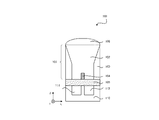
図1は、実施形態1における固体撮像素子の一部に配置された測距画素100の概略図である。測距画素100は、光の入射側より、導波路101、基板110を有している。基板110は、検出する波長帯域で吸収を有するSiなどの材料であり、Bイオン打ち込みなどで、内部の少なくとも一部の領域に、光を電荷に変換する光電変換部111、112が形成される。基板110には図示しない電極や配線部が設けられており、光電変換部111、112で発生した電荷は配線によって信号処理回路に転送される。図1の構造を上から見た形状は、例えば、正方形や円であり、2つの光電変換部111、112の形状は正方形や円を2分する中心線の両側の長方形や半円である。
Hereinafter, a solid-state imaging device according to an embodiment of the present invention, a distance measuring device using the same, and the like will be described with reference to the drawings. In that case, the same numerals are assigned to the same functions in all the drawings, and the repeated description thereof is omitted or simplified.
(Embodiment 1)
<Configuration of image sensor>
FIG. 1 is a schematic diagram of a ranging
導波路101は、コア102、及びコア102よりも屈折率が低い媒質から形成されるクラッド103からなっている。コア102の射出端には、導波路101を伝搬する光の一部を乱す散乱部104が設けられている。散乱部104は、光電変換部111と光電変換部112の間の画素分離部113の上に設けられる。散乱部104を設けることで、画素分離部113に入射する光を低減し、光電変換部111、112に入射する光を増加することができる。散乱部104を形成する材料は、周囲の媒質であるコア102を形成する材料よりも屈折率が低い必要がある。なぜなら、散乱部104を形成する材料がコア102を形成する材料よりも屈折率が高い場合、光が屈折率の高い散乱部104に誘引され、画素分離部113に入射する光が増えてしまうためである。
The
更に、導波路101と基板110の間に、コア102よりも屈折率が低い媒質で形成された層105が設けられている。以上の屈折率の大小関係を実現するためには、例えば、コア102をSiN、クラッド103、散乱部104、層105をSiO2で形成すればよい。層105を設けたことによって、測距画素100に大きな角度で入射する光束が多い場合でも、高精度な測距が可能な撮像素子が実現できる。以下でその理由を説明する。
Further, a
<測距の原理>
まず、本発明の固体撮像素子を用いた測距の原理について図2を用いて説明する。カメラレンズなどの結像光学系の射出瞳120上で、異なる位置を通った光束は、測距画素100に対し異なる角度で入射する光束となる。異なる角度で入射した光束は、導波路101への入射角に応じ、異なった導波モードに変換されて導波路101を伝搬する。導波モードは、導波路の持つ複数の固有モードの和で表される。固有モードは、導波路の形状と屈折率によって一意に決定される。導波路に入射した光束は、複数の固有モードと結合し、伝播する。入射角によって、導波モードを構成する固有モードの割合は異なり、それによって、各導波モードが有する波数ベクトルが異なる。一般に、高次のモードほど伝搬方向とは垂直な方向の波数成分が大きく、導波路内を斜めにジグザグに伝搬する。
<Principles of ranging>
First, the principle of distance measurement using the solid-state imaging device of the present invention will be described with reference to FIG. On the
導波路101の形状と屈折率を適切な値に設計することで、光束の入射角に応じて、異なる光電変換部に選択的に光束を導くことができる。図2のように、導波路101は、射出瞳のうち+x側領域からの光束121の光を、主に1次の固有モード131に結合させ、-x側領域からの光束122を、主に1次の固有モード132に結合させている。図2は、固有モード131と固有モード132の空間分布を示しており、直線部は振幅が小さい領域を、湾曲部は振幅が大きい領域を示している。1次の固有モード131に結合した光は導波路101中を真っすぐ伝搬して、光電変換部111に選択的に導かれる。同様に、1次の固有モード132に結合した光は光電変換部112に選択的に導かれる。光電変換部111で検出された像と光電変換部112で検出された像は信号処理部によって比較され、公知の手法を用いて距離が検出される。
By designing the shape and refractive index of the
<測距精度が向上する理由>
次に、コア102よりも屈折率の低い層105を設けたことによって測距精度が向上する理由について述べる。図3は、光束121、122の入射角度が大きい場合の、導波路101中の光の伝搬の様子を示す。光束121の入射角度が大きい場合、光束121は導波路101の入射端において位相が揃っていない状態で入射するため、1次の固有モード131に加えて、より高次の固有モード133にも結合する。前述したように、固有モード131に結合した光は、導波路101内を真っすぐ伝搬する。そして、導波路101の射出端において、光電変換部111側の領域151から真っすぐ層105に入る。一方、高次の固有モード133に結合した光は導波路内をジグザグに伝搬し、導波路101の射出端において、光電変換部111側の領域151と光電変換部112側の領域152から斜めに層105に入る。高次の固有モード133に結合した光のうち、領域151から射出される光を光141、領域152から射出される光を142と呼ぶ。
<Reasons for improved ranging accuracy>
Next, the reason why the ranging accuracy is improved by providing the
以上より、固有モード131に結合して真っすぐ伝搬する光と斜めに伝搬する光141が領域151から層105に入射し、斜めに伝搬する光142が領域152から層105に入射する。固有モード131に結合した真っすぐ伝搬する光は層105をそのまま真っすぐ伝搬し、光電変換部111に導かれる。一方、光141及び光142は層105中を斜めに伝搬する。この時、斜めに伝搬する光141及び光142の伝搬角度は、領域152において導波路内よりも大きくなる。なぜなら、層105の屈折率はコア102よりも小さいため、スネルの法則に従って、高屈折率のコア102から層105に入射する光は伝搬角が大きくなるように屈折するからである。そのため、光141及び光142は光電変換部111及び光電変換部112の外側に逃げ、光142が光電変換部112に入射することが防げる。従って、光束121のうち光電変換部111に入射する光の割合が相対的に増加する。
From the above, light propagating straightly coupled to the
同様に、光束122についても、層105を設けたことにより、導波路101の高次モードに結合した光が光電変換部111に入射することが防げ、より選択的に光束122を光電変換部112に導くことができる。以上より、層105を設けたことで、光束121と光束122を、各々選択的に光電変換部111と光電変換部112に導くことができ、高精度な測距が可能となる。また、導波路内の導波モードが異なるという特性を用いることで、特に画素が小さい場合でも(この場合、画素が小さいほど導波路が細くなるため、同じ次数の導波モードでも、斜めに伝搬するようになる)、異なる瞳領域を通過した光束を異なる光電変換部に導き、高精度な測距が可能となる。
Similarly, by providing the
<計算による効果の実証>
図4に測距画素100の導波路101を伝播し、光電変換部111及び光電変換部112に入射する光量の、入射角度依存性を示す。横軸は入射光(図2の光束121のようにx軸の正方向に傾いて入射した光を想定している)の入射角度、縦軸は光電変換部111、112に入射する光量を示している。実線は層105を設けた場合、破線は層105を設けなかった場合を示している。図4より、層105を設けたことで、特に大きな角度で入射した光束に対して、光電変換部112に入射する光量が減少していることが分かる。即ち、光電変換部111に選択的に入射する光の割合が増加している。これは、高次の固有モード133に結合した光が、層105によって光電変換部112に入射しないためである。同様の理由で、図2の光束122のようにx軸の負方向に傾いて入射した光を想定する場合は、光電変換部111に入射する光量が減少して光電変換部112に選択的に入射する光の割合が増加する。
<Demonstration of effect by calculation>
FIG. 4 shows the incident angle dependence of the amount of light that propagates through the
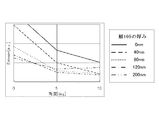
<低屈折率層の厚みについて>
層105において光142が光電変換部112に入射されることを防ぐために、層105の厚みは厚い方が好ましい。図5−1と図5−2は、光電変換部112に入射する光量の、層105に対する膜厚依存性を示す。図5−1より、層105の厚みが40nm以上であれば、光束121の入射角が比較的大きい時の光電変換部112へ入射する光量が低減できるため、高精度な測距が可能となる。図5−2より、光束121の入射角度が比較的小さい時でも、層105の厚みが120nm以上であれば、光電変換部112へ入射する光量が低減できるため、更に好ましい。ここでも、同様の理由で、図2のようにx軸の負方向に傾いて入射した光を想定する場合は、光電変換部111に入射する光量が減少して光電変換部112に選択的に入射する光の割合が増加する。また、層105は、複数の媒質から形成されている多層構造であっても良い。層105が多層構造の場合、層105全体の平均屈折率がコア102の平均屈折率よりも低ければ良い。
<About the thickness of the low refractive index layer>
In order to prevent the light 142 from being incident on the
<中央部と周辺部で層厚を変える>
測距画素100を複数配置する場合、層105は、固体撮像素子の周辺部に位置する測距画素100にのみ設けても良い。なぜなら、固体撮像素子の中央部よりも周辺部の方が測距画素100に入射する光束の入射角が大きいため、層105による測距精度向上の効果が大きいためである。同様の理由で、中央部に位置する測距画素よりも、周辺部に位置する測距画素の層105の厚みを厚くしても良い。ただし、後述する製造方法の観点からは、層105の厚みは全ての測距画素で同じである方が好ましい。
<Change the layer thickness between the central part and the peripheral part>
When a plurality of ranging
<測距画素の配置>
測距画素100を固体撮像素子の全画素として配置すれば、固体撮像素子の全領域の測距が可能となる。測距画素に含まれる光電変換部111、112で取得した信号を積算し、撮像画像の画像信号として利用することができる。各測距画素100を離散的に配置し、その間に撮像用画素を設けてもよい。この時、撮像用画素で取得した信号を用いて、近接する測距画素の画像信号を生成しても良い。複数の測距画素のうち、一部の測距画素を、図1に示す測距画素の構造をz軸周りに90度回転し、射出瞳をy軸方向に分割して測距を行う画素にしても良い。射出瞳をx軸方向に分割した画素では、x軸方向にコントラストを有する被写体の測距が可能となり、射出瞳をy軸方向に分割した画素では、y軸方向にコントラストを有する被写体の測距が可能となる。
<Range of ranging pixels>
If the ranging
<テーパ、マイクロレンズ、カラーフィルタ>
また、図1に示す測距画素では、散乱部104を導波路中に設けたが、散乱部104を設けなくても良い。但し、散乱部104を設けた方が画素分離部113に入射する光を減らすことができるため、好ましい。なお、導波路のコア102は、入射端に向かって径が広がるテーパ形状を有していることが望ましい。コア102をテーパ形状にすると、画素に入射した光束を、導波路のコア102に効率良く導くことができるため、三つの点から好ましい。一つ目は、光電変換部111、112に射出される光量が多くなり、像のSN比が向上する。二つ目は、画素間のクラッド103に、配線(不図示)を設ける空間を確保することができる。三つ目は、光が伝播する領域を画素の特定領域に限定し、隣接する画素に光が漏れて生じるクロストークを軽減することができる。
<Taper, microlens, color filter>
In the ranging pixel shown in FIG. 1, the scattering
また、図6のように、導波路101の上にマイクロレンズ106を配置しても良い。マイクロレンズ106を設けることにより、画素に入射した光束を、導波路のコア102に、更に効率良く導くことができる。各画素にはカラーフィルタを設けてもよい。これにより、導波路に入射する光の波長帯域を限定することができ、入射した光を所望の導波モードで伝搬させやすくなり、異なる瞳領域からの光を、異なる光電変換部に、より選択的に導くことができる。なお、図1では測距画素100中に設けられる光電変換部を2つとしたが、3つ以上の光電変換部が設けられていても良い。例えば、x軸方向に2分割、y軸方向に2分割した4つの光電変換部を用いれば、x軸方向とy軸方向の瞳分割を、同一画素内で行うことができる。射出瞳120をより詳細に分割することができ、より高精度な測距が行える。この構成において、散乱部104が設けられる場合、上から見た画素分離部113のパターンに対応して散乱部104が形成される。
Further, as shown in FIG. 6, the microlens 106 may be disposed on the
<製造方法>
続いて、固体撮像素子中の測距画素100の製造方法について図7を用いて説明する。まず、図7(a)のように、基板110(シリコン)に、光電変換部を形成する部分以外を覆うレジストをフォトリソグラフィによって作製し、イオン注入によって光電変換部111、112を作製する。アッシングでレジストを除去した後、図7(b)のように、基板上に、層105(SiO2)、後に散乱部104となる部分(SiO2)をスパッタなどによって成膜する。続いて、図7(c)のように、散乱部104を、フォトリソグラフィとドライエッチによって作製する。そして、アッシングでレジストを除去する。その後、導波路や配線を形成するプロセスは、上記特許文献1などに記載の公知の手法を用いればよい。導波路のコア102は、層105や散乱部104を形成するSiO2よりも屈折率の大きいSiNを用いればよい。
<Manufacturing method>
Next, a manufacturing method of the ranging
<測距装置及び撮像装置>
図8に、本発明の固体撮像素子を用いた測距装置190を示した。測距装置190は、被写体の像を固体撮像素子上に結像する光学系191、制御用のCPU192、測距画素100を有する固体撮像素子193、配線194、信号処理部195を有する。光電変換部111及び光電変換部112で取得した信号を配線194によって転送し、各々の像の出力信号を信号処理部195で比較することで被写体の距離情報を取得して、測距を行っている。以上の構成要素に加え、固体撮像素子で得られる画像を表示する表示装置、シャッター機構、システム制御部の動作用の定数、変数、各種プログラムなどを記憶するメモリ等を備えれば、図8の装置はカメラなどの撮像装置として捉えることもできる。こうしたカメラでは、測距装置の固体撮像素子193により、光学系で結像された被写体像を取得することもできる。
<Ranging device and imaging device>
FIG. 8 shows a
(実施形態2)
<散乱部が低屈折率膜の中>
図9は、実施形態2における固体撮像素子の一部に配置された測距画素200の概略図である。測距画素200は、実施形態1における測距画素100に対し、散乱部204が層105中に位置していることが異なる。更に、散乱部204を形成する材料は、層105中で、散乱部204の周囲を形成する材料よりも屈折率が低い。例えば、コア102をSiNで、クラッド及び層105のうち散乱部204以外の部分をSiONで、散乱部204をSiO2で形成すればよい。
(Embodiment 2)
<The scattering part is in the low refractive index film>
FIG. 9 is a schematic diagram of the ranging
<利点とその理由>
散乱部204を層105中に設けたことで、測距精度の向上に加えて感度が向上するため、更に好ましい。その理由について説明する。導波路101中に散乱部を設けた場合、散乱部の脇ではコア102の幅が狭くなる。そのため、導波路101を伝搬する光が狭い領域に閉じ込められ、導波路101の射出端では回折によって拡がり、層105に入射する。よって、光電変換部111や光電変換部112に入射する光量が減ってしまう。一方、層105中に散乱部204を設けた場合、コア102の幅は広いままである。そのため、導波路101の射出端での回折はあまり生じず、光は層105に真っすぐ入射する。層105に入射した光は散乱部204によって回折を生じるが、導波路101中の散乱部の影響に比べて小さい。以下に理由を述べる。
<Advantages and Reasons>
It is more preferable to provide the
層105は導波路101と異なり、コア102とクラッド103という屈折率差を持つ部分を有さない上、層105の屈折率はコア102の屈折率よりも低い。そのため、導波路101中に散乱部を設けた場合に比べ、狭い領域に光が閉じ込められていない。従って、散乱部を導波路101内に設けた場合よりも、散乱部204を層105内に設けた場合の方が、回折による光の拡がりが小さい。以上により、層105中に散乱部204を設けた方が更に好ましい。なお、散乱部204を層105中に設けた場合、散乱部204を形成する材料は、層105のうち、散乱部204の周囲を形成する材料よりも屈折率が低い必要がある。散乱部204を形成する材料として、層105のうちの散乱部204の周囲よりも高い屈折率の材料を用いると、導波路101から層105に入射した光が散乱部204に誘引され、画素分離部113に入射する光が増えてしまうためである。
Unlike the
<計算による効果の実証>
図10に測距画素200において、光電変換部111と光電変換部112に入射する光量の和(感度に相当)を示した。横軸は入射光の入射角度、縦軸は光電変換部に入射する光量を示している。実線は本実施形態の測距画素200、点線は実施形態1に記載の測距画素100、破線は図4にも比較例として示した層105を設けていない場合である。図10より、散乱部204を層105中に設けたことで、散乱部104を導波路101中に設けた場合に比べ、入射光量が増大していることが分かる。測距画素200の感度は、比較例として示した層105を設けていない場合とほぼ同等であり、特に、入射角が小さい時は測距画素200の方が高い。これは、前述したように層105中に散乱部204を設けた方が、導波路101中に散乱部を設けた場合に比べ、回折による光の拡がりが小さいためである。
<Demonstration of effect by calculation>
FIG. 10 shows the sum of the amounts of light incident on the
以上より、測距画素200を以下の構成とすることで、測距精度と感度がともに向上する固体撮像素子が提供できるため、更に好ましい。即ち、導波路101と基板110の間にコア102よりも屈折率が低い媒質で形成された層105を設け、層105中に、散乱部204の周囲の材料よりも屈折率が低い媒質で形成された散乱部204を設けた構成とすれば良い。
As described above, it is more preferable to provide the ranging
<散乱部の形状>
散乱部の幅は、狭いと画素分離部113に入射する光を十分に散乱できず、広いと光電変換部111、112に入射する光を減衰させてしまう。好ましくは、検出する波長の0.1倍から2倍程度であることが好ましい。散乱部の高さは、十分な散乱強度を稼ぐために、検出する波長の0.1倍以上であることが好ましい。なお、散乱部204は必ずしも層105に完全に包含されている必要はなく、図11のように層105と導波路101に跨っていても良い。すなわち、散乱部204の少なくとも一部が層105の中に含まれていればよい。散乱部204の下部は基板110に近い方が、感度が向上するため好ましい。なぜなら、散乱部204が基板110に近い方が、回折が生じる場所が基板110の上面に近いため、光が回折によって拡がる前に基板に入射するためである。
<Shape of scattering part>
If the width of the scattering portion is narrow, the light incident on the
図12は、光電変換部111と光電変換部112に入射する光量の和の、散乱部204の下面と基板110の上面間の距離に対する依存性を示す。図12より、散乱部204の下面と基板110の上面間の距離(すなわち散乱部と画素分離部の間の距離)は20nm以下であることが好ましい。また、固体撮像素子中に複数の測距画素200を設ける場合、散乱部204の形状を画素毎に変えても良い。例えば、固体撮像素子の中央部と周辺部では、入射する光束の角度が異なるため、それに応じて散乱部204の形状を変え、測距性能や感度を向上させることができる。具体的には、固体撮像素子の周辺部の画素では、散乱部204の形状(幅及び高さのうちの少なくとも一方)を大きくして、入射角が大きい光束に対する測距性能を向上させればよい。一方、固体撮像素子の中央部の画素では、散乱部204の形状を小さくして、入射角が小さい光束に対する感度を向上させればよい。このことは、実施形態1のように散乱部104を導波路101内に設けた場合についても言うことができる。
FIG. 12 shows the dependence of the sum of the amounts of light incident on the
<セルフアライメントプロセス>
特に、散乱部204を層105の最下部に設ける場合、以下に述べるセルフアラインの製造方法を用いることで、散乱部204と画素分離部113の位置ずれを防止できる。散乱部204が画素分離部113の位置ずれが少ないほど、画素分離部113に入射する光を低減できるため、好ましい。
<Self-alignment process>
In particular, when the
具体的に図13を用いて、測距画素200の製造方法を説明する。まず、図13(a)のように、基板110(シリコン)上に、後に散乱部204となる膜(第1の材料、例えばSiO2)を、散乱部204の高さまでスパッタなどによって成膜する。次に、図13(b)のように、フォトリソグラフィとエッチングによって、後に光電変換部111、112が形成される部分を露出し、開口部を設ける(除去工程)。続いて、図13(c)のように、イオン注入により光電変換部111、112を形成し、アッシングによってレジストを除去する(注入工程)。この工程により、画素分離部113の直上に、散乱部204が形成される。図7に記載の製造方法では、光電変換部111、112を形成するためのレジストパターン(図7(a))と、散乱部104を形成するためのレジストパターン(図7(c))が異なっていたため、2つのパターンの位置合わせが必要であった。しかし、図13のように、散乱部204を、光電変換部111、112を作製するためのマスクとして利用することで、高精度な位置合わせをせずに、散乱部204と画素分離部113を位置ずれ無く形成できる。
The manufacturing method of the ranging
次に、図13(d)のように層105を形成する材料(第1の材料よりも屈折率の大きい第2の材料、例えばSiON)をスパッタなどによって成膜し、CMPなどによって平坦化を行う(埋め込み工程)。なお、図13(d)からわかるように、この製造方法を用いた場合、層105のうち、光電変換部111、112の外側は散乱部204と同一の材料(SiO2)で形成される。このように、層105は必ずしも同一の材料で形成されていなくても、コア102を形成する材料よりも屈折率の低い材料で形成されていればよい。さらに、散乱部204を形成する材料の屈折率が、散乱部204の周囲の材料よりも低ければよい。図13の製造方法では、層105はSiO2とSiONで形成され、散乱部はSiO2で形成される。従って、コア102をSiNなどの、SiO2とSiONの双方よりも屈折率の高い材料で形成すればよい。
Next, as shown in FIG. 13D, a material for forming the layer 105 (a second material having a higher refractive index than the first material, for example, SiON) is formed by sputtering or the like, and planarized by CMP or the like. Perform (embedding step). As can be seen from FIG. 13D, when this manufacturing method is used, the outside of the
なお、図13(d)に示す工程の後、図13(e)のように再度のフォトリソグラフィとドライエッチ、アッシング、成膜、CMPによって層105の中において、光電変換部111、112の外側の部分に対応する部分に光吸収部207を設けても良い。光吸収部207は、例えば、有機材料や金属からなる。吸収部207によって、導波路101の高次の固有モード133に結合し、領域152から層105に入射する光142が、隣接画素などに入射してノイズとなることを防げる。吸収部207と光電変換部111、112の間に要求される位置合わせ精度は、散乱部204と画素分離部113の間に要求される位置合わせ精度に比べて小さい。従って、散乱部204をセルフアラインの製造方法で形成し、吸収部207は位置合わせを用いた複数回のフォトリソグラフィで形成することが好ましい。なお、吸収部207も層105に含まれるため、コア102よりも低い屈折率の材料で形成されている必要がある。以後の導波路や配線を形成するプロセスは、上記特許文献1などに記載の公知の手法を用いればよい。
After the step shown in FIG. 13D, outside the
固体撮像素子中に複数の測距画素200を設ける場合、吸収部207の形状を画素毎に変えても良い。例えば、固体撮像素子の中央部と周辺部では、入射する光束の角度が異なるため、それに応じて吸収部207の形状を変え、測距性能や感度を向上させることができる。具体的には、固体撮像素子の周辺部の画素では、吸収部207の形状を大きくして、入射角が大きい光束に対する測距性能を向上させればよい。一方、固体撮像素子の中央部の画素では、吸収部207の形状を小さくして、入射角が小さい光束に対する感度を向上させればよい。
When providing a plurality of ranging
以上、本発明の好ましい実施形態について説明したが、本発明はこれらの実施形態に限定されず、その要旨の範囲内で種々の変形及び変更が可能である。上述した本発明による撮像素子は、測距装置をはじめとして、測距装置を必要とするデジタルカメラなどの撮像装置に用いることができる。その際、撮像素子は、その構成に応じて、被写体の像を結像する光学系に対して適宜位置決めすればよい。 As mentioned above, although preferable embodiment of this invention was described, this invention is not limited to these embodiment, A various deformation | transformation and change are possible within the range of the summary. The above-described image sensor according to the present invention can be used in an imaging apparatus such as a distance measuring apparatus and a digital camera that requires the ranging apparatus. At that time, the image sensor may be appropriately positioned with respect to the optical system that forms an image of the subject according to the configuration.
100:測距画素(画素)、101:導波路、102:コア、105:層、111、112:光電変換部 100: ranging pixel (pixel), 101: waveguide, 102: core, 105: layer, 111, 112: photoelectric conversion unit
Claims (13)
前記導波路は、コア部材と、前記コア部材よりも屈折率が低い媒質により形成されるクラッド部材と、を有し、
前記複数の光電変換部と前記導波路の間に、前記導波路から射出された光が伝搬する、該導波路の前記コア部材よりも屈折率が低い媒質を有する層が設けられており、
前記複数の光電変換部の間の領域に対応する位置に、少なくとも一部が前記層の中に含まれている散乱部が設けられており、
前記散乱部は、周囲の媒質よりも屈折率が低い、光を透過する媒質からなることを特徴とする固体撮像素子。 A solid-state imaging device including a plurality of photoelectric conversion unit, and a waveguide provided on a light incident side than the plurality of photoelectric conversion unit, a pixel having,
The waveguide has a core member and a clad member formed of a medium having a refractive index lower than that of the core member,
A layer having a medium having a refractive index lower than that of the core member of the waveguide through which light emitted from the waveguide propagates is provided between the plurality of photoelectric conversion units and the waveguide .
At a position corresponding to a region between the plurality of photoelectric conversion units, a scattering unit at least part of which is included in the layer is provided,
The scattering unit is a solid-state imaging device characterized by being made of a light transmitting medium having a refractive index lower than that of the surrounding medium .
前記導波路は、コア部材と、前記コア部材よりも屈折率が低い媒質により形成されるクラッド部材と、を有し、
前記複数の光電変換部と前記導波路の間に、前記導波路から射出された光が伝搬する、該導波路の前記コア部材よりも屈折率が低い媒質を有する層が設けられており、
当該固体撮像素子の中央部に位置する画素よりも、当該固体撮像素子の周辺部に位置する画素の方が、前記層の厚みが厚くなっていることを特徴とする固体撮像素子。 A solid-state imaging device including a pixel having a plurality of photoelectric conversion units and a waveguide provided on the light incident side of the plurality of photoelectric conversion units,
The waveguide has a core member and a clad member formed of a medium having a refractive index lower than that of the core member,
A layer having a medium having a refractive index lower than that of the core member of the waveguide through which light emitted from the waveguide propagates is provided between the plurality of photoelectric conversion units and the waveguide.
The solid than the pixel positioned at the center of the imaging device, the solid-state towards the pixels located on the periphery of the image pickup device, the solid-state imaging device characterized in that the thickness of the layer is thicker.
前記導波路は、コア部材と、前記コア部材よりも屈折率が低い媒質により形成されるクラッド部材と、を有し、
前記複数の光電変換部と前記導波路の間に、前記導波路から射出された光が伝搬する、該導波路の前記コア部材よりも屈折率が低い媒質を有する層が設けられており、
前記複数の光電変換部の間の領域に対応する位置に、周囲の媒質よりも屈折率が低い媒質からなる散乱部が設けられており、
当該固体撮像素子の中央部に位置する画素よりも、当該固体撮像素子の周辺部に位置する画素の方が、前記散乱部の大きさが大きいことを特徴とする固体撮像素子。 A solid-state imaging device including a pixel having a plurality of photoelectric conversion units and a waveguide provided on the light incident side of the plurality of photoelectric conversion units,
The waveguide has a core member and a clad member formed of a medium having a refractive index lower than that of the core member,
A layer having a medium having a refractive index lower than that of the core member of the waveguide through which light emitted from the waveguide propagates is provided between the plurality of photoelectric conversion units and the waveguide.
A scattering portion made of a medium having a refractive index lower than that of the surrounding medium is provided at a position corresponding to a region between the plurality of photoelectric conversion portions,
Than the pixel positioned at the center of the solid-state imaging device, the solid-state towards the pixels located on the periphery of the image pickup device, wherein the scattering portion of it is a large size you wherein solid-state imaging device.
前記導波路は、コア部材と、前記コア部材よりも屈折率が低い媒質により形成されるクラッド部材と、を有し、
前記複数の光電変換部と前記導波路の間に、前記導波路から射出された光が伝搬する、該導波路の前記コア部材よりも屈折率が低い媒質を有する層が設けられており、
前記複数の光電変換部の間の領域に対応する位置に、周囲の媒質よりも屈折率が低い媒質からなる散乱部が設けられており、
前記層の中において、前記光電変換部よりも外側の部分に対応する部分に光吸収部が形成されており、
当該固体撮像素子の中央部に位置する画素よりも、当該固体撮像素子の周辺部に位置する画素の方が、前記光吸収部の大きさが大きいことを特徴とする固体撮像素子。 A solid-state imaging device including a pixel having a plurality of photoelectric conversion units and a waveguide provided on the light incident side of the plurality of photoelectric conversion units,
The waveguide has a core member and a clad member formed of a medium having a refractive index lower than that of the core member,
A layer having a medium having a refractive index lower than that of the core member of the waveguide through which light emitted from the waveguide propagates is provided between the plurality of photoelectric conversion units and the waveguide.
A scattering portion made of a medium having a refractive index lower than that of the surrounding medium is provided at a position corresponding to a region between the plurality of photoelectric conversion portions,
In the layer, a light absorbing portion is formed in a portion corresponding to a portion outside the photoelectric conversion portion,
Than the pixel positioned at the center of the solid-state imaging device, towards the pixels located on the periphery of the solid-state imaging device, the light absorbing portion is large size you wherein solid-state imaging device.
前記複数の光電変換部からの複数の出力信号を用いて被写体の距離情報を取得する信号処理部と、を有することを特徴とする測距装置。 And the solid-state image sensor of any crab of claims 1 to 11,
A distance measuring apparatus comprising: a signal processing unit that acquires distance information of a subject using a plurality of output signals from the plurality of photoelectric conversion units.
Priority Applications (2)
| Application Number | Priority Date | Filing Date | Title |
|---|---|---|---|
| JP2012241700A JP6124555B2 (en) | 2012-11-01 | 2012-11-01 | Solid-state imaging device and distance measuring device using the same |
| US14/043,582 US9307170B2 (en) | 2012-11-01 | 2013-10-01 | Solid-state image sensor and range finder using the same |
Applications Claiming Priority (1)
| Application Number | Priority Date | Filing Date | Title |
|---|---|---|---|
| JP2012241700A JP6124555B2 (en) | 2012-11-01 | 2012-11-01 | Solid-state imaging device and distance measuring device using the same |
Publications (3)
| Publication Number | Publication Date |
|---|---|
| JP2014093343A JP2014093343A (en) | 2014-05-19 |
| JP2014093343A5 JP2014093343A5 (en) | 2015-12-10 |
| JP6124555B2 true JP6124555B2 (en) | 2017-05-10 |
Family
ID=50546769
Family Applications (1)
| Application Number | Title | Priority Date | Filing Date |
|---|---|---|---|
| JP2012241700A Expired - Fee Related JP6124555B2 (en) | 2012-11-01 | 2012-11-01 | Solid-state imaging device and distance measuring device using the same |
Country Status (2)
| Country | Link |
|---|---|
| US (1) | US9307170B2 (en) |
| JP (1) | JP6124555B2 (en) |
Families Citing this family (10)
| Publication number | Priority date | Publication date | Assignee | Title |
|---|---|---|---|---|
| JP6226606B2 (en) | 2013-07-23 | 2017-11-08 | キヤノン株式会社 | Color filter array, solid-state imaging device, imaging device |
| JP2015164284A (en) | 2014-01-28 | 2015-09-10 | キヤノン株式会社 | Solid-state image sensor, movement information acquisition apparatus and imaging apparatus |
| JP6173259B2 (en) | 2014-06-02 | 2017-08-02 | キヤノン株式会社 | Photoelectric conversion device and imaging system |
| JP6444066B2 (en) | 2014-06-02 | 2018-12-26 | キヤノン株式会社 | Photoelectric conversion device and imaging system |
| JP2016031993A (en) * | 2014-07-28 | 2016-03-07 | キヤノン株式会社 | Solid state image pickup device and camera |
| JP6558998B2 (en) | 2015-07-28 | 2019-08-14 | キヤノン株式会社 | Imaging device |
| JP2017069553A (en) * | 2015-09-30 | 2017-04-06 | キヤノン株式会社 | Solid-state imaging device, method of manufacturing the same, and camera |
| US10204943B2 (en) | 2016-08-10 | 2019-02-12 | Canon Kabushiki Kaisha | Image sensor, method of manufacturing the same, and camera with pixel including light waveguide and insulation film |
| JP6895724B2 (en) * | 2016-09-06 | 2021-06-30 | キヤノン株式会社 | Image sensor and image sensor |
| US10014338B2 (en) * | 2016-10-12 | 2018-07-03 | Samsung Electronics Co., Ltd. | Image sensor |
Family Cites Families (17)
| Publication number | Priority date | Publication date | Assignee | Title |
|---|---|---|---|---|
| JP2006190766A (en) * | 2005-01-05 | 2006-07-20 | Sony Corp | Solid-state imaging element |
| JP2008091771A (en) | 2006-10-04 | 2008-04-17 | Matsushita Electric Ind Co Ltd | Solid-state image pickup device and its manufacturing method |
| US7822300B2 (en) * | 2007-11-20 | 2010-10-26 | Aptina Imaging Corporation | Anti-resonant reflecting optical waveguide for imager light pipe |
| JP5422889B2 (en) * | 2007-12-27 | 2014-02-19 | 株式会社ニコン | Solid-state imaging device and imaging apparatus using the same |
| JP2009272596A (en) * | 2008-04-09 | 2009-11-19 | Sony Corp | Solid-state imaging device, method of manufacturing the same, and electronic instrument |
| JP5428451B2 (en) * | 2009-03-30 | 2014-02-26 | ソニー株式会社 | Solid-state imaging device, manufacturing method thereof, and imaging device |
| JP5539014B2 (en) * | 2009-05-21 | 2014-07-02 | キヤノン株式会社 | Solid-state image sensor |
| US7923799B2 (en) * | 2009-06-09 | 2011-04-12 | Aptina Imaging Corporation | Image sensors with light guides |
| JP2011040454A (en) * | 2009-08-07 | 2011-02-24 | Sony Corp | Solid-state imaging device, method for manufacturing the solid-state imaging device, and electronic apparatus |
| JP5538803B2 (en) * | 2009-10-07 | 2014-07-02 | キヤノン株式会社 | Solid-state imaging device and camera equipped with the same |
| JP2012043939A (en) * | 2010-08-18 | 2012-03-01 | Sony Corp | Imaging element and imaging apparatus |
| JP5574926B2 (en) | 2010-11-17 | 2014-08-20 | キヤノン株式会社 | Solid-state image sensor |
| JP5834398B2 (en) * | 2010-11-22 | 2015-12-24 | 株式会社ニコン | Imaging device and imaging apparatus |
| JP5736755B2 (en) * | 2010-12-09 | 2015-06-17 | ソニー株式会社 | SOLID-STATE IMAGING DEVICE, ITS MANUFACTURING METHOD, AND ELECTRONIC DEVICE |
| JP5812610B2 (en) | 2011-01-18 | 2015-11-17 | キヤノン株式会社 | Solid-state imaging device and imaging system having solid-state imaging device |
| JP5956718B2 (en) * | 2011-01-20 | 2016-07-27 | キヤノン株式会社 | Imaging device and imaging apparatus |
| JP2012182332A (en) * | 2011-03-02 | 2012-09-20 | Sony Corp | Imaging element and imaging device |
-
2012
- 2012-11-01 JP JP2012241700A patent/JP6124555B2/en not_active Expired - Fee Related
-
2013
- 2013-10-01 US US14/043,582 patent/US9307170B2/en active Active
Also Published As
| Publication number | Publication date |
|---|---|
| JP2014093343A (en) | 2014-05-19 |
| US9307170B2 (en) | 2016-04-05 |
| US20140118589A1 (en) | 2014-05-01 |
Similar Documents
| Publication | Publication Date | Title |
|---|---|---|
| JP6124555B2 (en) | Solid-state imaging device and distance measuring device using the same | |
| JP5506517B2 (en) | Solid-state image sensor | |
| JP5812610B2 (en) | Solid-state imaging device and imaging system having solid-state imaging device | |
| JP5631176B2 (en) | Solid-state image sensor and camera | |
| JP6172982B2 (en) | Imaging apparatus and camera system | |
| US9443891B2 (en) | Solid-state image sensor and imaging device | |
| JP6091204B2 (en) | Solid-state imaging device and imaging apparatus | |
| JP6271900B2 (en) | Solid-state imaging device and imaging apparatus using the same | |
| US9565381B2 (en) | Solid-state image sensor and image-capturing device | |
| US8610228B2 (en) | Solid-state image sensor | |
| CN105280655A (en) | Photoelectric conversion apparatus and imaging system | |
| US9219855B2 (en) | Image sensor, ranging apparatus, and imaging apparatus | |
| JP6034629B2 (en) | Image pickup device and image pickup apparatus using the same | |
| JP4532968B2 (en) | Focus detection device | |
| JP6001030B2 (en) | Solid-state image sensor and camera | |
| JP2017054991A (en) | Imaging device and imaging apparatus using the same | |
| JP4708721B2 (en) | Solid-state image sensor | |
| JP2010074218A (en) | Solid-state image pickup element and method of manufacturing the same, and image pickup apparatus using the solid-state image pickup element | |
| KR20090051353A (en) | Method for manufacturing an image sensor | |
| JP2008147568A (en) | Image sensor and imaging device |
Legal Events
| Date | Code | Title | Description |
|---|---|---|---|
| A521 | Request for written amendment filed |
Free format text: JAPANESE INTERMEDIATE CODE: A523 Effective date: 20151019 |
|
| A621 | Written request for application examination |
Free format text: JAPANESE INTERMEDIATE CODE: A621 Effective date: 20151019 |
|
| A977 | Report on retrieval |
Free format text: JAPANESE INTERMEDIATE CODE: A971007 Effective date: 20160816 |
|
| A131 | Notification of reasons for refusal |
Free format text: JAPANESE INTERMEDIATE CODE: A131 Effective date: 20160823 |
|
| A521 | Request for written amendment filed |
Free format text: JAPANESE INTERMEDIATE CODE: A523 Effective date: 20161017 |
|
| TRDD | Decision of grant or rejection written | ||
| A01 | Written decision to grant a patent or to grant a registration (utility model) |
Free format text: JAPANESE INTERMEDIATE CODE: A01 Effective date: 20170307 |
|
| A61 | First payment of annual fees (during grant procedure) |
Free format text: JAPANESE INTERMEDIATE CODE: A61 Effective date: 20170404 |
|
| R151 | Written notification of patent or utility model registration |
Ref document number: 6124555 Country of ref document: JP Free format text: JAPANESE INTERMEDIATE CODE: R151 |
|
| RD03 | Notification of appointment of power of attorney |
Free format text: JAPANESE INTERMEDIATE CODE: R3D03 |
|
| LAPS | Cancellation because of no payment of annual fees |