JP6118045B2 - Semiconductor memory device - Google Patents
Semiconductor memory device Download PDFInfo
- Publication number
- JP6118045B2 JP6118045B2 JP2012170078A JP2012170078A JP6118045B2 JP 6118045 B2 JP6118045 B2 JP 6118045B2 JP 2012170078 A JP2012170078 A JP 2012170078A JP 2012170078 A JP2012170078 A JP 2012170078A JP 6118045 B2 JP6118045 B2 JP 6118045B2
- Authority
- JP
- Japan
- Prior art keywords
- management information
- block
- blocks
- predetermined number
- block group
- Prior art date
- Legal status (The legal status is an assumption and is not a legal conclusion. Google has not performed a legal analysis and makes no representation as to the accuracy of the status listed.)
- Expired - Fee Related
Links
Images


Landscapes
- Techniques For Improving Reliability Of Storages (AREA)
Description
本発明は、半導体記憶装置に関する。 The present invention relates to a semiconductor memory device.
メモリコントローラと、フラッシュメモリ等のメモリセルアレイとを備えたメモリシステムが実用化されている。NAND型のフラッシュメモリ等においては、製造時に発生する先天性不良ブロックや、出荷後の通常使用によって発生する後天性不良ブロックが、ランダムに存在する。これらの不良ブロックを避けて使用する必要があるため、所定の管理情報によって不良ブロックの位置が管理される。 A memory system including a memory controller and a memory cell array such as a flash memory has been put into practical use. In a NAND flash memory or the like, there are randomly acquired congenital defective blocks that occur at the time of manufacture, and acquired defective blocks that occur due to normal use after shipment. Since it is necessary to avoid these bad blocks and use them, the position of the bad block is managed by predetermined management information.
制御対象メモリであるメモリセルアレイ内に管理情報を格納しようとすると、格納先のブロックが先天性不良ブロックであった場合や、格納時には先天性不良ブロックではなかったがその後に後天性不良ブロックとなった場合に、管理情報の一部又は全部のデータが破壊又は喪失されてしまう可能性がある。また、管理情報を更新するために新たな管理情報を書き込んでいる最中に、ユーザの誤操作等によって強制的に電源が遮断されてしまうと、管理情報の一部又は全部のデータが破壊又は喪失されてしまう可能性がある。管理情報が破壊又は喪失されると、その後はメモリシステムの正常動作が阻害される。 If you try to store management information in the memory cell array that is the memory to be controlled, if the storage block is a congenital defective block, or it was not a congenital defective block at the time of storage, it will later become an acquired defective block. In this case, some or all of the management information data may be destroyed or lost. Also, if the power is forcibly shut down due to a user's mistaken operation while writing new management information to update the management information, some or all of the data in the management information is destroyed or lost. There is a possibility of being. If the management information is destroyed or lost, then the normal operation of the memory system is hindered.
そこで、背景技術に係るメモリシステムでは、制御対象メモリとは別の専用の不揮発性メモリを用意し、当該不揮発性メモリ内に管理情報を格納することによって、管理情報の破壊等が防止されている。他の方法として、メモリコントローラ内の不揮発のメモリ領域に管理情報を格納し、あるいはDIPスイッチの設定によって管理情報をメモリコントローラに与えることで、管理情報の破壊等が防止されている。 Therefore, in the memory system according to the background art, by preparing a dedicated non-volatile memory different from the control target memory and storing the management information in the non-volatile memory, destruction of the management information is prevented. . As another method, management information is stored in a non-volatile memory area in the memory controller, or management information is given to the memory controller by setting a DIP switch, thereby preventing destruction of the management information.
なお、下記特許文献1には、コントローラとフラッシュメモリとを備えたメモリシステムが開示されている。不良ブロックのリスト等を含む管理情報は、複数の分割片に分割されて、各分割片がフラッシュメモリ内に個別に保存されている。また、コントローラ内には、DRAM等の揮発性メモリを用いた管理メモリが実装されている。複数の分割片がフラッシュメモリから管理メモリに読み出されることにより、管理メモリ内に管理情報が保存される。
上述したように背景技術に係るメモリシステムでは、制御対象メモリとは別の専用の不揮発性メモリ内に管理情報が格納される。従って、制御対象メモリとは別に専用の不揮発性メモリを追加する必要があるため、製造コストが増大するとともに制御が複雑化する。 As described above, in the memory system according to the background art, management information is stored in a dedicated non-volatile memory different from the control target memory. Therefore, since it is necessary to add a dedicated non-volatile memory in addition to the control target memory, the manufacturing cost increases and the control becomes complicated.
本発明はかかる問題を解決するために成されたものであり、不良ブロックの存在や強制的な電源遮断等に起因して正常動作が阻害されるという事態を回避しつつ、管理情報を制御対象メモリに格納することが可能な半導体記憶装置を得ることを目的とする。 The present invention has been made to solve such a problem, and management information is controlled while avoiding a situation in which normal operation is hindered due to the presence of a defective block or forced power shutdown. An object is to obtain a semiconductor memory device that can be stored in a memory.
本発明の第1の態様に係る半導体記憶装置は、それぞれがデータの消去単位である複数のブロックを有する記憶部と、前記記憶部を制御する制御部と、を備え、前記記憶部が有する全ブロックには、前記制御部が前記記憶部を管理するために必要な管理情報を格納するためのブロックとして限定的に割り当てられた、4個以上である第1所定数個のブロックから成る第1ブロック群と、第1ブロック群以外の第2ブロック群と、が含まれ、第1ブロック群の中から前記制御部によって選択された、3個以上かつ第1所定数個未満である第2所定数個のブロックの各々に、同一内容の管理情報が格納されており、管理情報は、第1管理情報と、第1管理情報よりも書き換え頻度の高い第2管理情報と、を含み、第1管理情報は第1ブロック群内に格納され、第2管理情報は第2ブロック群内に格納され、第1管理情報には、第2ブロック群内において第2管理情報を格納しているブロックを示す第1位置情報が含まれ、前記制御部は、正常な第1管理情報が格納されている正常ブロックを、第1ブロック群の中から特定し、ある1個の正常ブロックに格納されている第1管理情報と、当該第1管理情報に記述されている第1ブロック群内の他の2個のブロックを示す第2位置情報に基づき特定される2個の第1管理情報とを用いて多数決を行うことによって、1個の妥当な第1管理情報を特定し、当該妥当な第1管理情報に含まれている第1位置情報に基づいて、第2ブロック群の中から第2管理情報を取得することを特徴とするものである。
A semiconductor memory device according to a first aspect of the present invention includes a storage unit having a plurality of blocks, each of which is a data erasing unit, and a control unit that controls the storage unit, and all of the storage unit has A first block composed of a first predetermined number of blocks of four or more, which is limitedly assigned as a block for storing management information necessary for the control unit to manage the storage unit. A second predetermined group that includes a block group and a second block group other than the first block group, and that is selected by the control unit from the first block group and that is three or more and less than the first predetermined number Management information having the same content is stored in each of several blocks. The management information includes first management information and second management information having a higher rewrite frequency than the first management information. Management information in the first block group The second management information is stored in the second block group, and the first management information includes first position information indicating a block storing the second management information in the second block group, The control unit identifies a normal block in which normal first management information is stored from the first block group, the first management information stored in a certain normal block, and the first block By making a majority decision using two pieces of first management information specified based on the second position information indicating the other two blocks in the first block group described in the management information, The first management information is identified, and the second management information is acquired from the second block group based on the first position information included in the valid first management information. It is.
第1の態様に係る半導体記憶装置によれば、4個以上である第1所定数個のブロックから成る第1ブロック群が、管理情報を格納するためのブロックとして限定的に割り当てられている。そして、第1ブロック群の中から制御部によって選択された、3個以上かつ第1所定数個未満である第2所定数個のブロックの各々に、同一内容の管理情報が格納されている。従って、第2所定数個のブロックに格納されている第2所定数個の第1管理情報のうちの一つが破壊又は喪失された場合であっても、制御部は、破壊又は喪失されていない残りの第1管理情報を、記憶部から取得することができる。その結果、不良ブロックの存在や強制的な電源遮断等に起因して正常動作が阻害されるという事態を回避しつつ、管理情報を制御対象メモリに格納することが可能となる。
また、第1の態様に係る半導体記憶装置によれば、管理情報は、第1管理情報と、第1管理情報よりも書き換え頻度の高い第2管理情報とを含む。そして、第1管理情報は第1ブロック群内に格納され、第2管理情報は第2ブロック群内に格納される。書き換え頻度に応じて管理情報を第1管理情報と第2管理情報とに分割し、限定的に割り当てられた第1ブロック群内には、書き換え頻度の低い第1管理情報を格納することにより、第1ブロック群内ではデータの書き換えが頻繁には発生しない。その結果、第1ブロック群内における後天性不良ブロックの発生が抑制されるため、装置の信頼性を向上することが可能となる。
また、第1の態様に係る半導体記憶装置によれば、制御部は、正常な第1管理情報が格納されている正常ブロックを、第1ブロック群の中から特定する。そして、特定したある1個の正常ブロックに格納されている第1管理情報と、当該第1管理情報に記述されている第1ブロック群内の他の2個のブロックを示す第2位置情報に基づき特定される2個の第1管理情報とを用いて多数決を行うことによって、1個の妥当な第1管理情報を特定する。従って、更新が繰り返されることで第1ブロック群内に複数バージョンの第1管理情報が格納されている場合であっても、妥当な第1管理情報を適切に特定することが可能となる。また、多数決を行う対象を3個の第1管理情報に限定することによって、簡易に多数決を行うことができるため、処理の所要時間を短縮することが可能となる。また、多数決を行う対象を、更新時に併せて書き込まれた同一内容の第1管理情報に限定できるため、多数決によって妥当な第1管理情報を特定できる可能性を高めることが可能となる。
According to the semiconductor memory device according to the first aspect, the first block group including the first predetermined number of blocks of four or more is limitedly assigned as a block for storing the management information. Then, the management information having the same content is stored in each of the second predetermined number of blocks, which is selected by the control unit from the first block group and is less than the first predetermined number. Therefore, even if one of the second predetermined number of first management information stored in the second predetermined number of blocks is destroyed or lost, the control unit is not destroyed or lost. The remaining first management information can be acquired from the storage unit. As a result, it is possible to store the management information in the control target memory while avoiding the situation where the normal operation is hindered due to the presence of a defective block or forced power cut-off.
Further, according to the semiconductor memory device according to the first aspect, the management information includes the first management information and the second management information that is rewritten more frequently than the first management information. The first management information is stored in the first block group, and the second management information is stored in the second block group. By dividing the management information into the first management information and the second management information according to the rewrite frequency, and storing the first management information with a low rewrite frequency in the limited first block group, Data rewriting does not occur frequently in the first block group. As a result, since the occurrence of acquired defective blocks in the first block group is suppressed, the reliability of the apparatus can be improved.
Further, according to the semiconductor memory device according to the first aspect, the control unit identifies a normal block in which normal first management information is stored from the first block group. The first management information stored in one specified normal block and the second position information indicating the other two blocks in the first block group described in the first management information By making a majority decision using the two pieces of first management information specified based on the information, one piece of reasonable first management information is specified. Therefore, even when multiple versions of the first management information are stored in the first block group by repeating the update, it is possible to appropriately specify the appropriate first management information. In addition, by limiting the target of majority decision to the three pieces of first management information, the majority decision can be easily made, so that the time required for processing can be shortened. In addition, since the target of the majority decision can be limited to the first management information having the same contents written at the time of the update, it is possible to increase the possibility that the appropriate first management information can be specified by the majority decision.
本発明の第2の態様に係る半導体記憶装置は、第1の態様に係る半導体記憶装置において特に、第2管理情報には、不良ブロックを示す位置情報が含まれることを特徴とするものである。
The semiconductor memory device according to the second aspect of the present invention is characterized in that, in the semiconductor memory device according to the first aspect , the second management information includes position information indicating a defective block. .
第2の態様に係る半導体記憶装置によれば、第2管理情報には、不良ブロックを示す位置情報が含まれる。従って、制御部は、第1管理情報を記憶部から読み出すことによって、第2管理情報を格納しているブロックを示す位置情報を取得でき、また、当該位置情報に基づいて第2管理情報を記憶部から読み出すことによって、不良ブロックを示す位置情報を取得することが可能となる。
According to the semiconductor memory device according to the second aspect , the second management information includes position information indicating a defective block. Therefore, the control unit can acquire the position information indicating the block storing the second management information by reading the first management information from the storage unit, and stores the second management information based on the position information. By reading from the part, it is possible to acquire position information indicating a defective block.
本発明の第3の態様に係る半導体記憶装置は、第2の態様に係る半導体記憶装置において特に、第1管理情報には、第1ブロック群内の不良ブロックを示す位置情報が含まれ、第2管理情報には、第2ブロック群内の不良ブロックを示す位置情報が含まれることを特徴とするものである。
In the semiconductor memory device according to the third aspect of the present invention, particularly in the semiconductor memory device according to the second aspect, the first management information includes position information indicating a defective block in the first block group. The 2 management information includes position information indicating defective blocks in the second block group.
第3の態様に係る半導体記憶装置によれば、第1管理情報には、第1ブロック群内の不良ブロックを示す位置情報が含まれ、第2管理情報には、第2ブロック群内の不良ブロックを示す位置情報が含まれる。従って、第1ブロック群内で後天性不良ブロックが発生した場合には、第1管理情報のみを更新すればよく、第2管理情報の更新を省略することができる。同様に、第2ブロック群内で後天性不良ブロックが発生した場合には、第2管理情報のみを更新すればよく、第1管理情報の更新を省略することができる。
According to the semiconductor memory device of the third aspect, the first management information includes position information indicating a defective block in the first block group, and the second management information includes a defect in the second block group. Position information indicating a block is included. Therefore, when an acquired defective block occurs in the first block group, only the first management information needs to be updated, and the update of the second management information can be omitted. Similarly, when an acquired defective block occurs in the second block group, only the second management information needs to be updated, and the update of the first management information can be omitted.
本発明の第4の態様に係る半導体記憶装置は、第1〜第3のいずれか一つの態様に係る半導体記憶装置において特に、第2ブロック群の中から選択された、2個以上である第3所定数個のブロックの各々に、同一内容の第2管理情報が格納されており、第1管理情報には、第2管理情報を格納している第3所定数個のブロックを示す第1位置情報が含まれており、前記制御部は、妥当な第1管理情報に含まれている第1位置情報に基づいて第3所定数個のブロックを特定し、当該第3所定数個のブロックに格納されている第3所定数個の第2管理情報の中から、1個の第2管理情報を取得することを特徴とするものである。
The semiconductor memory device according to the fourth aspect of the present invention is, in the semiconductor memory device according to any one of the first to third aspects, particularly two or more selected from the second block group. in each of the three predetermined number of blocks, the second management information of the same content are stored, the first management information, first shows a third predetermined number of blocks storing the
第4の態様に係る半導体記憶装置によれば、第2ブロック群の中から選択された、2個以上である第3所定数個のブロックの各々に、同一内容の第2管理情報が格納されている。そして、制御部は、妥当な第1管理情報に含まれている第1位置情報に基づいて第3所定数個のブロックを特定し、当該第3所定数個のブロックに格納されている第3所定数個の第2管理情報の中から、1個の第2管理情報を取得する。従って、第3所定数個のブロックに格納されている第3所定数個の第2管理情報のうちの一つが破壊又は喪失された場合であっても、制御部は、破壊又は喪失されていない残りの第2管理情報を、記憶部から取得することができる。その結果、不良ブロックの存在や強制的な電源遮断等に起因して正常動作が阻害されるという事態を回避しつつ、管理情報を制御対象メモリに格納することが可能となる。
According to the semiconductor memory device of the fourth aspect, the second management information having the same contents is stored in each of the third predetermined number of blocks that are two or more selected from the second block group. ing. Then, the control unit, third identifying a predetermined number of blocks based on the first position information included in the valid first management information, third stored in said third predetermined number of blocks One second management information is acquired from a predetermined number of second management information. Therefore, even if one of the third predetermined number of second management information stored in the third predetermined number of blocks is destroyed or lost, the control unit is not destroyed or lost. The remaining second management information can be acquired from the storage unit. As a result, it is possible to store the management information in the control target memory while avoiding the situation where the normal operation is hindered due to the presence of a defective block or forced power cut-off.
本発明の第5の態様に係る半導体記憶装置は、第1〜第3のいずれか一つの態様に係る半導体記憶装置において特に、第2ブロック群の中から選択された、2個以上である第3所定数個のブロックに、バージョンが異なる第3所定数個の第2管理情報が格納されており、第1管理情報には、第2管理情報を格納している第3所定数個のブロックを示す第1位置情報が含まれており、前記制御部は、妥当な第1管理情報に含まれている第1位置情報に基づいて第3所定数個のブロックを特定し、当該第3所定数個のブロックに格納されている第3所定数個の第2管理情報の中から、1個の第2管理情報を取得することを特徴とするものである。
The semiconductor memory device according to the fifth aspect of the present invention is, in the semiconductor memory device according to any one of the first to third aspects, particularly two or more selected from the second block group. 3 Predetermined number of blocks stores third predetermined number of second management information having different versions, and the first management information includes third predetermined number of blocks storing second management information the includes a first position information indicating the control unit, third identifying a predetermined number of blocks based on the first position information included in the valid first management information, said third predetermined One second management information is obtained from a third predetermined number of second management information stored in several blocks.
第5の態様に係る半導体記憶装置によれば、第2ブロック群の中から選択された、2個以上である第3所定数個のブロックに、バージョンが異なる第3所定数個の第2管理情報が格納されている。そして、制御部は、妥当な第1管理情報に含まれている第1位置情報に基づいて第3所定数個のブロックを特定し、当該第3所定数個のブロックに格納されている第3所定数個の第2管理情報の中から、1個の第2管理情報を取得する。従って、第3所定数個のブロックに格納されている第3所定数個の第2管理情報のうちの一つが破壊又は喪失された場合であっても、制御部は、破壊又は喪失されていない残りの第2管理情報を、記憶部から取得することができる。その結果、不良ブロックの存在や強制的な電源遮断等に起因して正常動作が阻害されるという事態を回避しつつ、管理情報を制御対象メモリに格納することが可能となる。
According to the semiconductor memory device according to a fifth aspect, selected from among the second block group, the third predetermined number of blocks is two or more, the second management version several different third predetermined Information is stored. Then, the control unit, third identifying a predetermined number of blocks based on the first position information included in the valid first management information, third stored in said third predetermined number of blocks One second management information is acquired from a predetermined number of second management information. Therefore, even if one of the third predetermined number of second management information stored in the third predetermined number of blocks is destroyed or lost, the control unit is not destroyed or lost. The remaining second management information can be acquired from the storage unit. As a result, it is possible to store the management information in the control target memory while avoiding the situation where the normal operation is hindered due to the presence of a defective block or forced power cut-off.
本発明の第6の態様に係る半導体記憶装置は、第1〜第5のいずれか一つの態様に係る半導体記憶装置において特に、前記制御部は、第1ブロック群の中から、先天性不良ブロックを除外することにより、正常ブロックを特定することを特徴とするものである。
The semiconductor memory device according to a sixth aspect of the present invention is the semiconductor memory device according to any one of the first to fifth aspects, and in particular, the control unit includes a congenital defective block from the first block group. The normal block is specified by excluding.
第6の態様に係る半導体記憶装置によれば、制御部は、第1ブロック群の中から先天性不良ブロックを除外することにより、正常ブロックを特定する。従って、先天性不良ブロックが正常ブロックとして特定されるという事態を回避できるため、妥当な第1管理情報を適切に特定することが可能となる。
According to the semiconductor memory device of the sixth aspect, the control unit specifies a normal block by excluding a congenital defective block from the first block group. Therefore, it is possible to avoid a situation in which a congenital defective block is specified as a normal block, and it is possible to appropriately specify appropriate first management information.
本発明の第7の態様に係る半導体記憶装置は、第1〜第6のいずれか一つの態様に係る半導体記憶装置において特に、前記制御部は、第1ブロック群の中から、所定の無効フラグが付加された無効ブロックを除外することにより、正常ブロックを特定することを特徴とするものである。
The semiconductor memory device according to a seventh aspect of the present invention is the semiconductor memory device according to any one of the first to sixth aspects, and in particular, the control unit includes a predetermined invalid flag from the first block group. The normal block is specified by excluding the invalid block to which is added.
第7の態様に係る半導体記憶装置によれば、制御部は、第1ブロック群の中から無効ブロックを除外することにより、正常ブロックを特定する。従って、無効ブロックが正常ブロックとして特定されるという事態を回避できるため、妥当な第1管理情報を適切に特定することが可能となる。
According to the semiconductor memory device of the seventh aspect, the control unit specifies the normal block by excluding the invalid block from the first block group. Therefore, since it is possible to avoid a situation where an invalid block is specified as a normal block, it is possible to appropriately specify appropriate first management information.
本発明の第8の態様に係る半導体記憶装置は、第1〜第7のいずれか一つの態様に係る半導体記憶装置において特に、前記制御部は、第1ブロック群の中から、格納している第1管理情報にデータの誤りが生じている異常ブロックを除外することにより、正常ブロックを特定することを特徴とするものである。
The semiconductor memory device according to an eighth aspect of the present invention is the semiconductor memory device according to any one of the first to seventh aspects, and in particular, the control unit stores the first block group. A normal block is specified by excluding an abnormal block in which a data error has occurred in the first management information.
第8の態様に係る半導体記憶装置によれば、制御部は、第1ブロック群の中から異常ブロックを除外することにより、正常ブロックを特定する。従って、異常ブロックが正常ブロックとして特定されるという事態を回避できるため、妥当な第1管理情報を適切に特定することが可能となる。
According to the semiconductor memory device of the eighth aspect, the control unit specifies the normal block by excluding the abnormal block from the first block group. Accordingly, it is possible to avoid a situation in which an abnormal block is specified as a normal block, and it is possible to appropriately specify appropriate first management information.
本発明の第9の態様に係る半導体記憶装置は、それぞれがデータの消去単位である複数のブロックを有する記憶部と、前記記憶部を制御する制御部と、を備え、前記記憶部が有する全ブロックには、前記制御部が前記記憶部を管理するために必要な管理情報を格納するためのブロックとして限定的に割り当てられた、4個以上である第1所定数個のブロックから成る第1ブロック群と、第1ブロック群以外の第2ブロック群と、が含まれ、第1ブロック群の中から前記制御部によって選択された、3個以上かつ第1所定数個未満である第2所定数個のブロックの各々に、同一内容の管理情報が格納されており、管理情報は、第1管理情報と、第1管理情報よりも書き換え頻度の高い第2管理情報と、を含み、第1管理情報は第1ブロック群内に格納され、第2管理情報は第2ブロック群内に格納され、前記制御部は、第1管理情報を更新する必要が生じた場合には、第1ブロック群の中で第2所定数個の空きブロックを確保し、当該第2所定数個の空きブロックの各々に、更新後の第1管理情報をそれぞれ書き込み、第2所定数個の空きブロックの中の一の空きブロックに書き込む第1管理情報に、第2所定数個の空きブロックの中の他の空きブロックを示す位置情報を含めて書き込むことを特徴とするものである。
A semiconductor memory device according to a ninth aspect of the present invention includes a storage unit having a plurality of blocks, each of which is a data erasing unit, and a control unit that controls the storage unit, and all of the storage unit has A first block consisting of a first predetermined number of blocks of four or more, which is assigned to the block in a limited manner as a block for storing management information necessary for the control unit to manage the storage unit and block group, and a second block group other than the first block group, contains, selected by the control unit from the first block group, three or more and the first second predetermined a predetermined less than several Management information having the same content is stored in each of several blocks. The management information includes first management information and second management information having a higher rewrite frequency than the first management information. Management information is the first block group The second management information is stored in the second block group, and the control unit, when it becomes necessary to update the first management information, is a second predetermined number of blocks in the first block group. The first block is reserved, the updated first management information is written in each of the second predetermined number of free blocks, and the first predetermined block is written in one of the second predetermined number of free blocks. The management information is written together with position information indicating other empty blocks among the second predetermined number of empty blocks.
第9の態様に係る半導体記憶装置によれば、4個以上である第1所定数個のブロックから成る第1ブロック群が、管理情報を格納するためのブロックとして限定的に割り当てられている。そして、第1ブロック群の中から制御部によって選択された、3個以上かつ第1所定数個未満である第2所定数個のブロックの各々に、同一内容の管理情報が格納されている。従って、第2所定数個のブロックに格納されている第2所定数個の第1管理情報のうちの一つが破壊又は喪失された場合であっても、制御部は、破壊又は喪失されていない残りの第1管理情報を、記憶部から取得することができる。その結果、不良ブロックの存在や強制的な電源遮断等に起因して正常動作が阻害されるという事態を回避しつつ、管理情報を制御対象メモリに格納することが可能となる。
また、第9の態様に係る半導体記憶装置によれば、管理情報は、第1管理情報と、第1管理情報よりも書き換え頻度の高い第2管理情報とを含む。そして、第1管理情報は第1ブロック群内に格納され、第2管理情報は第2ブロック群内に格納される。書き換え頻度に応じて管理情報を第1管理情報と第2管理情報とに分割し、限定的に割り当てられた第1ブロック群内には、書き換え頻度の低い第1管理情報を格納することにより、第1ブロック群内ではデータの書き換えが頻繁には発生しない。その結果、第1ブロック群内における後天性不良ブロックの発生が抑制されるため、装置の信頼性を向上することが可能となる。
また、第9の態様に係る半導体記憶装置によれば、制御部は、第1管理情報を更新する必要が生じた場合には、第1ブロック群の中で第2所定数個の空きブロックを確保し、当該第2所定数個の空きブロックの各々に、更新後の第1管理情報をそれぞれ書き込む。これにより、更新後においても、同一内容の第2所定個数の第1管理情報を、第1ブロック群に格納することが可能となる。
また、第9の態様に係る半導体記憶装置によれば、制御部は、第2所定数個の空きブロックの中の一の空きブロックに書き込む第1管理情報に、第2所定数個の空きブロックの中の他の空きブロックを示す位置情報を含めて書き込む。従って、多数決を行う対象を、更新時に併せて書き込まれた同一内容の第1管理情報に限定できるため、多数決によって妥当な第1管理情報を特定できる可能性を高めることが可能となる。
本発明の第10の態様に係る半導体記憶装置は、第9の態様に係る半導体記憶装置において特に、前記制御部は、第1管理情報の誤り検出符号を、第1管理情報に含めて書き込むことを特徴とするものである。
第10の態様に係る半導体記憶装置によれば、制御部は、第1管理情報の誤り検出符号を、第1管理情報に含めて書き込む。従って、誤り検出符号を用いて多数決を行うことができ、その結果、妥当な第1管理情報を適切に特定する精度を向上することが可能となる。また、誤り検出符号を用いてデータの誤りが生じているか否かを判定することができ、その結果、第1ブロック群の中から正常ブロックを特定する際に、データの誤りが生じている異常ブロックを除外することが可能となる。
According to the semiconductor memory device of the ninth aspect, the first block group composed of the first predetermined number of blocks of four or more is limitedly assigned as a block for storing management information. Then, selected by the control unit from the first block group, in each of three or more and a second predetermined number of blocks first are given below a few, the management information of the same content is stored. Therefore, even if one of the second predetermined number of first management information stored in the second predetermined number of blocks is destroyed or lost, the control unit is not destroyed or lost. The remaining first management information can be acquired from the storage unit. As a result, it is possible to store the management information in the control target memory while avoiding the situation where the normal operation is hindered due to the presence of a defective block or forced power cut-off.
According to the semiconductor memory device of the ninth aspect, the management information includes the first management information and the second management information that is rewritten more frequently than the first management information. The first management information is stored in the first block group, and the second management information is stored in the second block group. By dividing the management information into the first management information and the second management information according to the rewrite frequency, and storing the first management information with a low rewrite frequency in the limited first block group, Data rewriting does not occur frequently in the first block group. As a result, since the occurrence of acquired defective blocks in the first block group is suppressed, the reliability of the apparatus can be improved.
According to the semiconductor memory device of the ninth aspect, when the control unit needs to update the first management information, the control unit allocates the second predetermined number of empty blocks in the first block group. The updated first management information is written in each of the second predetermined number of empty blocks. Thereby, even after the update, the second predetermined number of first management information having the same contents can be stored in the first block group.
According to the semiconductor memory device of the ninth aspect, the control unit adds the second predetermined number of empty blocks to the first management information to be written in one empty block of the second predetermined number of empty blocks. Is written including position information indicating other empty blocks. Therefore, since the target of majority decision can be limited to the first management information having the same contents written together at the time of update, it is possible to increase the possibility of specifying appropriate first management information by majority decision.
A semiconductor memory device according to a tenth aspect of the present invention is the semiconductor memory device according to the ninth aspect, in which the control unit writes the error detection code of the first management information in the first management information. It is characterized by.
According to the semiconductor memory device of the tenth aspect, the control unit writes the error detection code of the first management information included in the first management information. Therefore, a majority decision can be made using the error detection code, and as a result, it is possible to improve the accuracy of appropriately identifying the appropriate first management information. In addition, it is possible to determine whether or not a data error has occurred using an error detection code. As a result, when a normal block is identified from the first block group, an abnormality in which a data error has occurred Blocks can be excluded.
本発明の第11の態様に係る半導体記憶装置は、第9又は第10の態様に係る半導体記憶装置において特に、前記制御部は、第1ブロック群の中から、先天性不良ブロックを除外することにより、空きブロックを確保することを特徴とするものである。
A semiconductor memory device according to an eleventh aspect of the present invention is the semiconductor memory device according to the ninth or tenth aspect, in which the control unit excludes a congenital defective block from the first block group. Thus, an empty block is secured.
第11の態様に係る半導体記憶装置によれば、制御部は、第1ブロック群の中から、先天性不良ブロックを除外することにより、空きブロックを確保する。従って、更新後の第1管理情報を書き込むブロックとして、先天性不良ブロックが選択されるという事態を回避することが可能となる。
According to the semiconductor memory device of the eleventh aspect, the control unit secures an empty block by excluding the congenital defective block from the first block group. Therefore, it is possible to avoid a situation where a congenital defective block is selected as a block in which the updated first management information is written.
本発明の第12の態様に係る半導体記憶装置は、第9〜第11のいずれか一つの態様に係る半導体記憶装置において特に、前記制御部は、第1ブロック群の中から、後天性不良ブロックを除外することにより、空きブロックを確保することを特徴とするものである。
A semiconductor memory device according to a twelfth aspect of the present invention is the semiconductor memory device according to any one of the ninth to eleventh aspects, in particular, the control unit includes an acquired defective block from the first block group. This is characterized in that an empty block is secured by excluding.
第12の態様に係る半導体記憶装置によれば、制御部は、第1ブロック群の中から、後天性不良ブロックを除外することにより、空きブロックを確保する。従って、更新後の第1管理情報を書き込むブロックとして、後天性不良ブロックが選択されるという事態を回避することが可能となる。
According to the semiconductor memory device in the twelfth aspect, the control unit secures an empty block by excluding the acquired defective block from the first block group. Therefore, it is possible to avoid a situation where an acquired defective block is selected as a block in which the updated first management information is written.
本発明の第13の態様に係る半導体記憶装置は、第9〜第12のいずれか一つの態様に係る半導体記憶装置において特に、前記制御部は、第1ブロック群の中から、更新前の第1管理情報が格納されている第2所定数個のブロックを除外することにより、空きブロックを確保することを特徴とするものである。
The semiconductor memory device according to a thirteenth aspect of the present invention is the semiconductor memory device according to any one of the ninth to twelfth aspects, and in particular, the control unit includes a first block group from the first block group before the update. An empty block is secured by excluding the second predetermined number of blocks in which one management information is stored.
第13の態様に係る半導体記憶装置によれば、制御部は、第1ブロック群の中から、更新前の第1管理情報が格納されている第2所定数個のブロックを除外することにより、空きブロックを確保する。従って、第1管理情報の更新処理中にユーザの誤操作等によって強制的に電源が遮断され、それによって更新後の第1管理情報が消去された場合等であっても、更新前の第1管理情報は記憶部内に残されているため、それを用いて再起動を行うことが可能となる。
According to the semiconductor memory device of the thirteenth aspect, the control unit excludes, from the first block group, the second predetermined number of blocks in which the first management information before update is stored, Reserve free blocks. Accordingly, even when the power is forcibly shut down due to a user's erroneous operation or the like during the update process of the first management information, and the first management information after the update is thereby deleted, the first management before the update is performed. Since the information remains in the storage unit, it can be restarted using the information.
本発明の第14の態様に係る半導体記憶装置は、第9〜第13のいずれか一つの態様に係る半導体記憶装置において特に、前記制御部は、第2所定数個の空きブロックの中の1個の空きブロックへの第1管理情報の書き込みが完了すると、更新前の第1管理情報が格納されていた第2所定数個のブロックの中の1個のブロックに対して、所定の無効フラグを付加することを特徴とするものである。
The semiconductor memory device according to the fourteenth aspect of the present invention is the semiconductor memory device according to any one of the ninth to thirteenth aspects, and in particular, the control unit is configured to select one of the second predetermined number of empty blocks. When the writing of the first management information to the empty blocks is completed, a predetermined invalid flag is set for one block in the second predetermined number of blocks in which the first management information before the update is stored. Is added.
第14の態様に係る半導体記憶装置によれば、制御部は、1個の空きブロックへの第1管理情報の書き込みが完了すると、更新前の第1管理情報が格納されていた1個のブロックに対して、所定の無効フラグを付加する。これにより、第1管理情報が格納されているブロックとして、少なくとも第2所定数個のブロックを常に確保することが可能となる。しかも、データを消去するのではなく無効フラグを付加するため、消去に伴うメモリセルへのストレスを回避できる。その結果、第1ブロック群内における後天性不良ブロックの発生が抑制されるため、装置の信頼性を向上することが可能となる。
According to the semiconductor memory device of the fourteenth aspect, when the writing of the first management information to one empty block is completed, the control unit stores one block in which the first management information before update is stored. For this, a predetermined invalid flag is added. As a result, at least the second predetermined number of blocks can always be secured as the blocks in which the first management information is stored. Moreover, since an invalid flag is added instead of erasing data, stress on the memory cell due to erasure can be avoided. As a result, since the occurrence of acquired defective blocks in the first block group is suppressed, the reliability of the apparatus can be improved.
本発明の第15の態様に係る半導体記憶装置は、第9〜第13のいずれか一つの態様に係る半導体記憶装置において特に、前記制御部は、第2所定数個の空きブロックの中の1個の空きブロックへの第1管理情報の書き込みが完了すると、更新前の第1管理情報が格納されていた第2所定数個のブロックの中の1個のブロックに対して、データの消去を行うことを特徴とするものである。
A semiconductor memory device according to a fifteenth aspect of the present invention is the semiconductor memory device according to any one of the ninth to thirteenth aspects, and in particular, the control unit is configured to select one of the second predetermined number of empty blocks. When the writing of the first management information to the empty blocks is completed, the data is erased from one of the second predetermined number of blocks in which the first management information before the update is stored. It is characterized by doing.
第15の態様に係る半導体記憶装置によれば、制御部は、第2所定数個の空きブロックの中の1個の空きブロックへの第1管理情報の書き込みが完了すると、更新前の第1管理情報が格納されていた第2所定数個のブロックの中の1個のブロックに対して、データの消去を行う。これにより、第1管理情報が格納されているブロックとして、少なくとも第2所定数個のブロックを常に確保することが可能となる。
According to the semiconductor memory device in the fifteenth aspect, when the writing of the first management information to one empty block in the second predetermined number of empty blocks is completed, the control unit completes the first before update. Data is erased from one of the second predetermined number of blocks in which the management information is stored. As a result, at least the second predetermined number of blocks can always be secured as the blocks in which the first management information is stored.
本発明の第16の態様に係る半導体記憶装置は、第1〜第15のいずれか一つの態様に係る半導体記憶装置において特に、先天性不良ブロックを除外した第1所定数個のブロックが、第1ブロック群として割り当てられることを特徴とするものである。
The semiconductor memory device according to the sixteenth aspect of the present invention is the semiconductor memory device according to any one of the first to fifteenth aspects, in particular, the first predetermined number of blocks excluding the congenital defective blocks are It is assigned as one block group.
第16の態様に係る半導体記憶装置によれば、先天性不良ブロックを除外した第1所定数個のブロックが、第1ブロック群として割り当てられる。従って、第1ブロック群を構成するブロックとして、必ず第1所定数個のブロックを確保できるため、装置の信頼性を向上することが可能となる。
According to the semiconductor memory device in the sixteenth aspect, the first predetermined number of blocks excluding the congenital defective blocks are assigned as the first block group. Therefore, since the first predetermined number of blocks can be secured as the blocks constituting the first block group, the reliability of the apparatus can be improved.
本発明によれば、不良ブロックの存在や強制的な電源遮断等に起因して正常動作が阻害されるという事態を回避しつつ、管理情報を制御対象メモリに格納することが可能な半導体記憶装置を得ることができる。 According to the present invention, a semiconductor storage device capable of storing management information in a control target memory while avoiding a situation in which normal operation is hindered due to the presence of a defective block or forced power-off Can be obtained.
以下、本発明の実施の形態について、図面を用いて詳細に説明する。なお、異なる図面において同一の符号を付した要素は、同一又は相応する要素を示すものとする。 Hereinafter, embodiments of the present invention will be described in detail with reference to the drawings. In addition, the element which attached | subjected the same code | symbol in different drawing shall show the same or corresponding element.
<実施の形態1>
図1は、本発明の実施の形態1に係る半導体記憶装置1の構成を簡略化して示す図である。半導体記憶装置1は、メモリコントローラ2(制御部)と、メモリコントローラ2によって制御される制御対象メモリ3(記憶部)とを備えている。制御対象メモリ3は、不揮発性のメモリであり、例えばNAND型フラッシュメモリによって構成されている。
<
FIG. 1 is a diagram showing a simplified configuration of a
図2は、制御対象メモリ3のメモリ空間の一部を抜き出して示す図である。メモリ空間は、複数のブロックB1〜BNに分割されている。ブロックは、データの消去の単位である。制御対象メモリ3が有する全ブロックB1〜BNは、第1ブロック群R1と第2ブロック群R2とに分類されている。
FIG. 2 is a diagram illustrating a part of the memory space of the
第1ブロック群R1は、後述する第1管理情報を格納するためのブロックの集合であり、全ブロックB1〜BNの中から限定された特定の複数個のブロックが、第1ブロック群R1として割り当てられている。本実施の形態の例では、ブロックB1〜B10の合計10個のブロックが、第1ブロック群R1として割り当てられている。 The first block group R1 is a set of blocks for storing first management information to be described later, and a specific plurality of blocks limited among all the blocks B1 to BN are assigned as the first block group R1. It has been. In the example of the present embodiment, a total of 10 blocks B1 to B10 are allocated as the first block group R1.
第2ブロック群R2は、第1ブロック群R1以外のブロックの集合である。第2ブロック群R2には、ユーザが使用する任意のデータが格納される。また、第2ブロック群R2には、後述する第2管理情報が格納される。 The second block group R2 is a set of blocks other than the first block group R1. Arbitrary data used by the user is stored in the second block group R2. The second block group R2 stores second management information to be described later.
管理情報は、メモリコントローラ2が制御対象メモリ3を管理するために必要な情報であり、本実施の形態の例において、管理情報は第1管理情報と第2管理情報とに分割されている。
The management information is information necessary for the
第1管理情報には、第2管理情報を格納しているブロックの所在を示す位置情報が含まれる。位置情報としては、例えばブロックアドレスが用いられる。 The first management information includes position information indicating the location of the block storing the second management information. As the position information, for example, a block address is used.
また、第1管理情報には、誤り検出符号が含まれる。誤り検出符号は、その第1管理情報にデータの誤りが生じているか否かの判定に使用される。また、誤り検出符号は、妥当な第1管理情報を特定するための多数決(詳細は後述する)に使用される。誤り検出符号としては、チェックサム、CRC(Cyclic Redundancy Check)、又はメッセージダイジェスト等を使用することができる。本実施の形態の例では、誤り検出符号としてCRCが使用される。 The first management information includes an error detection code. The error detection code is used to determine whether or not a data error has occurred in the first management information. Further, the error detection code is used for majority decision (details will be described later) for specifying appropriate first management information. As an error detection code, a checksum, CRC (Cyclic Redundancy Check), message digest, or the like can be used. In the example of the present embodiment, CRC is used as the error detection code.
また、第1管理情報には、固有のID情報(本明細書において「管理情報ID」と称す)が含まれる。管理情報IDは、第1管理情報のバージョンを示すものであり、第1管理情報が更新される度に管理情報IDの値も更新される。本実施の形態の例では、第1管理情報が更新される度に「1」ずつインクリメントされる整数値が、管理情報IDとして使用される。管理情報IDは、妥当な第1管理情報を特定するための多数決(詳細は後述する)に使用される。 The first management information includes unique ID information (referred to as “management information ID” in this specification). The management information ID indicates the version of the first management information, and the value of the management information ID is updated every time the first management information is updated. In the example of the present embodiment, an integer value incremented by “1” each time the first management information is updated is used as the management information ID. The management information ID is used in a majority vote (details will be described later) for specifying appropriate first management information.
また、第1管理情報には、第1ブロック群R1の中に不良ブロックが存在している場合に、その不良ブロックの所在を示す位置情報が含まれる。不良ブロックには、制御対象メモリ3の製造時に発生する先天性不良ブロックと、出荷後の通常使用によって発生する後天性不良ブロックとが含まれる。
The first management information includes position information indicating the location of the defective block when there is a defective block in the first block group R1. The defective blocks include congenital defective blocks that occur when the
第1管理情報を更新する場合には、第1ブロック群R1のうち、更新前の第1管理情報を格納しているブロックとは異なるブロックに、更新後の第1管理情報が書き込まれる。書き込み中に該当ブロックが後天性不良ブロックとなった場合には、第1ブロック群R1内の別のブロックに、更新後の第1管理情報が書き込まれる。 When the first management information is updated, the updated first management information is written in a block different from the block storing the first management information before the update in the first block group R1. When the corresponding block becomes an acquired defective block during writing, the updated first management information is written to another block in the first block group R1.
第2管理情報には、第2ブロック群R2の中に不良ブロックが存在している場合に、その不良ブロックの所在を示す位置情報が含まれる。また、第2管理情報には、汎用領域の場所や制御対象メモリ3へのアクセス速度等の、メモリコントローラ2が制御対象メモリ3を管理するために必要な様々な情報が含まれる。
The second management information includes position information indicating the location of the defective block when there is a defective block in the second block group R2. The second management information includes various information necessary for the
第2管理情報を更新する場合には、第2ブロック群R2のうち、更新前の第2管理情報を格納しているブロックと同一のブロックに、更新後の第2管理情報が上書きされる。書き込み中に該当ブロックが後天性不良ブロックとなった場合には、第2ブロック群R2内の別の任意のブロック(但し不良ブロックは除く)に、更新後の第2管理情報が書き込まれる。第1管理情報には第2管理情報を格納しているブロックの位置情報が含まれているため、第2管理情報を格納するブロックが変更された場合には、第1管理情報を更新する必要がある。 When the second management information is updated, the updated second management information is overwritten on the same block as the block storing the second management information before the update in the second block group R2. When the corresponding block becomes an acquired defective block during writing, the updated second management information is written in another arbitrary block (excluding the defective block) in the second block group R2. Since the first management information includes the position information of the block storing the second management information, it is necessary to update the first management information when the block storing the second management information is changed. There is.
各管理情報内に含めている情報の性質上、第2管理情報は第1管理情報よりも更新頻度(書き換え頻度)が高いといえる。例えば、第2ブロック群R2の中のユーザデータ領域内で後天性不良ブロックが発生した場合には、第2管理情報は更新する必要があるが、第1管理情報の更新は不要である。第2ブロック群R2のブロック数は第1ブロック群R1のブロック数よりもはるかに大きいため、第2ブロック群R2内で後天性不良ブロックが発生する確率は、第1ブロック群R1内で後天性不良ブロックが発生する確率よりも十分に高い。従って、第1管理情報は更新せずに第2管理情報を更新するという状況は、逆の状況よりも多く発生する。 From the nature of the information included in each management information, it can be said that the second management information has a higher update frequency (rewrite frequency) than the first management information. For example, when an acquired bad block occurs in the user data area in the second block group R2, the second management information needs to be updated, but the first management information does not need to be updated. Since the number of blocks in the second block group R2 is much larger than the number of blocks in the first block group R1, the probability that an acquired defective block will occur in the second block group R2 is acquired in the first block group R1. It is sufficiently higher than the probability that a bad block will occur. Therefore, the situation of updating the second management information without updating the first management information occurs more frequently than the opposite situation.
図3は、使用が想定されている制御対象メモリ3の種類を示す図である。本実施の形態では、ページサイズ、ブロックサイズ、総ブロック数、読み出しサイクル、及び先天性不良フラグの位置が異なる、複数種類(この例では4種類)のメモリの使用が想定されている。なお、各メモリには、メモリの種類を識別するための固有のID情報(本明細書において「メモリID」と称す)が付与されている。メモリIDには、ページサイズ及びブロックサイズの情報が含まれている。
FIG. 3 is a diagram illustrating the types of the
以下、本実施の形態に係る半導体記憶装置1に関して、(1)管理情報の格納例、(2)管理情報の取得処理、(3)管理情報の更新処理を、順に説明する。
Hereinafter, (1) management information storage example, (2) management information acquisition process, and (3) management information update process will be described in order with respect to the
(1)管理情報の格納例
本実施の形態に係る半導体記憶装置1では、第1ブロック群R1に属する10個のブロックB1〜B10の中から選択された3個のブロックに、同一内容の第1管理情報が格納される。但し、「10個」及び「3個」の値は一例であり、この値には限定されない。
(1) Example of storing management information In the
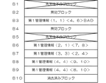
図4は、第1ブロック群R1を示す図である。この例において、ブロックB1,B5は先天性不良ブロックであり、ブロックB2,B4は無効ブロック(詳細は後述する)である。 FIG. 4 is a diagram illustrating the first block group R1. In this example, blocks B1 and B5 are congenital defective blocks, and blocks B2 and B4 are invalid blocks (details will be described later).
ブロックB3,B6〜B9には第1管理情報が格納されている。第1管理情報に付した丸括弧内の数字は、管理情報ID値(左側)及びCRC値(右側)を示している。説明の便宜上、第1管理情報を書き込む際のCRC値は、管理情報ID値と同一の値をとるものとする。データの誤りが生じていない正常ブロックに関しては、CRC値と管理情報ID値とは一致し、一方、後天性不良ブロックになったこと等に起因してデータの誤りが生じている異常ブロックに関しては、CRC値と管理情報ID値とは一致しない。この例において、ブロックB6に格納されている第1管理情報(2,1)に関しては、CRC値と管理情報ID値とが一致していない。従って、ブロックB6は後天性不良ブロックである。 Blocks B3, B6 to B9 store first management information. The numbers in parentheses attached to the first management information indicate the management information ID value (left side) and the CRC value (right side). For convenience of explanation, it is assumed that the CRC value when the first management information is written takes the same value as the management information ID value. For a normal block in which no data error has occurred, the CRC value and the management information ID value match, while on the other hand, for an abnormal block in which a data error has occurred due to an acquired bad block, etc. The CRC value does not match the management information ID value. In this example, regarding the first management information (2, 1) stored in the block B6, the CRC value does not match the management information ID value. Therefore, the block B6 is an acquired defective block.
また、図4に示した例では、最新の第1管理情報は第1管理情報(4,4)である。ここで、第1管理情報(4,4)はブロックB8,B9の2個のブロックにしか格納されていないが、その理由は、ブロックB10のデータを消去した後、第1管理情報(4,4)を書き込む前に、ユーザによって電源が強制的に遮断された状況を想定しているためである。従って、ブロックB10は消去済みブロックとなっている。 In the example shown in FIG. 4, the latest first management information is the first management information (4, 4). Here, the first management information (4, 4) is stored only in the two blocks B8 and B9. The reason is that after the data in the block B10 is erased, the first management information (4, 4) is stored. This is because it is assumed that the power supply is forcibly cut off by the user before 4) is written. Therefore, the block B10 is an erased block.
また、ブロックB3内に表記している「BAD」は、第1管理情報をブロックB3に書き込む際に、ブロックB3が後天性不良ブロックとなったことを表している。但し、ブロックB3に格納されている第1管理情報(1,1)に関しては、管理情報ID値とCRC値とが一致している。そのため、管理情報ID値とCRC値との比較によっては、ブロックB3が後天性不良ブロックであるとは判定できない。 Further, “BAD” written in the block B3 indicates that the block B3 has become an acquired defective block when the first management information is written in the block B3. However, regarding the first management information (1, 1) stored in the block B3, the management information ID value matches the CRC value. Therefore, it cannot be determined that the block B3 is an acquired defective block by comparing the management information ID value and the CRC value.
なお、第1管理情報をブロックに書き込む際にそのブロックが後天性不良ブロックとなった場合には、その第1管理情報に付した管理情報ID値をメモリコントローラが保持しておき、それ以降に第1管理情報を更新する際には、その管理情報ID値を使用しないようにしても良い。これにより、サイクリックカウンタを用いて管理情報ID値を生成する場合に、後天性不良ブロックに格納されている古い第1管理情報と、それ以降に更新された新たな第1管理情報とで、管理情報ID値が偶然に一致するという事態が回避される。 When the first management information is written into the block, if the block becomes an acquired defect block, the memory controller holds the management information ID value attached to the first management information, and thereafter When updating the first management information, the management information ID value may not be used. Thereby, when generating the management information ID value using the cyclic counter, the old first management information stored in the acquired defective block and the new first management information updated after that, A situation in which the management information ID values coincide by chance is avoided.
図5は、ブロックB1〜B10の各ブロックに関して、ブロック内のページの割り当てを示す図である。1ブロックは複数のページに分割されている。ページは、データの書き込み及び読み出しの単位である。この例では、ページP0は先天性不良フラグが付加されるページであり、ページPNは無効フラグが付加されるページであり、ページPMは第1管理情報が書き込まれるページである。なお、第1管理情報はブロック内の複数のページに格納されていても良い。 FIG. 5 is a diagram showing allocation of pages in the blocks with respect to the blocks B1 to B10. One block is divided into a plurality of pages. A page is a unit for writing and reading data. In this example, page P0 is a page to which a congenital defect flag is added, page PN is a page to which an invalid flag is added, and page PM is a page to which first management information is written. The first management information may be stored on a plurality of pages in the block.
あるブロックが先天性不良ブロックである場合には、そのブロックのページP0に先天性不良フラグが付加される。先天性不良フラグが付加されるページは、図3に示したように制御対象メモリ3の種類によって異なる。
When a certain block is a congenital defective block, a congenital defective flag is added to page P0 of the block. The page to which the congenital defect flag is added differs depending on the type of the
あるブロックのデータが無効である場合には、そのブロックのページPNに無効フラグが付加される。無効フラグが付加されるページは、制御対象メモリ3の種類によらず共通である。
When data of a certain block is invalid, an invalid flag is added to the page PN of that block. The page to which the invalid flag is added is common regardless of the type of the
(2)管理情報の取得処理
図6〜11は、半導体記憶装置1の起動時にメモリコントローラ2が実行する管理情報の取得処理を順に示す図である。第1ブロック群R1は、図4に示した状態になっているものとする。
(2) Management Information Acquisition Processing FIGS. 6 to 11 are diagrams sequentially illustrating management information acquisition processing executed by the
まず、メモリコントローラ2は、メモリIDを要求するリードコマンドを制御対象メモリ3に発行することにより、制御対象メモリ3からメモリIDを取得する。メモリIDにはページサイズ及びブロックサイズの情報が含まれているため、メモリIDを取得することにより、制御対象メモリ3内の任意のページへのアクセスが可能となる。
First, the
<先天性不良ブロックの探索ステップ>
次に図6を参照して、メモリコントローラ2は、第1ブロック群R1に属する全てのブロックB1〜B10を対象として、先天性不良ブロックを探索する。具体的には、ブロックB1〜B10の各ブロックに関して、先天性不良フラグの格納ページにアクセスすることにより、各ブロックが先天性不良ブロックであるか否かを判定する。
<Step of searching for congenital defective blocks>
Next, referring to FIG. 6, the
この時点では制御対象メモリ3の種類が判明していないため、先天性不良フラグの格納ページを一意には特定できない。従って、メモリコントローラ2は、使用が想定されている全種類のメモリに関する先天性不良フラグの格納ページに順にアクセスする。図3に示した例では、メモリコントローラ2は、第0ページの第0バイト、第0ページの第2048バイト、第128ページの第0バイト、及び第256ページの第8192バイトに順にアクセスすることにより、いずれかの格納ページに先天性不良フラグが付加されているか否かを判定する。また、その際の制御対象メモリ3へのアクセス速度は、使用が想定されている全種類のメモリを正常に動作させることが可能な最も遅い速度とする。図3に示した例では、4種類のメモリのうち最も遅い50nsの読み出しサイクルでアクセスを行う。
At this time, since the type of the
なお、メモリIDとメモリ種類とを関連付けるテーブル情報を予め作成してメモリコントローラ2内に保持しておき、メモリコントローラ2が制御対象メモリ3からメモリIDを取得した後に当該テーブル情報を参照することにより、メモリ種類を特定するように構成してもよい。この場合には、特定したメモリ種類に対応したアクセス速度で、特定したメモリ種類に対応した格納ページにアクセスすることにより、先天性不良フラグが付加されているか否かを判定することができる。
Note that table information that associates the memory ID with the memory type is created in advance and stored in the
探索の結果、ブロックB1〜B10内に先天性不良ブロックが存在している場合には、メモリコントローラ2は、そのブロックを取得対象ブロックの候補から除外する。図6に示した例では、先天性不良ブロックであるブロックB1,B5が候補から除外される。このステップで除外されずに残ったブロックB2〜B4,B6〜B10を、本明細書において「良ブロック」と称す。
As a result of the search, if a congenital defective block exists in the blocks B1 to B10, the
<無効ブロックの探索ステップ>
次に図7を参照して、メモリコントローラ2は、良ブロックB2〜B4,B6〜B10を対象として、無効ブロックを探索する。具体的には、各良ブロックに関して、無効フラグの格納ページ(図5に示したページPN)にアクセスすることにより、各良ブロックが無効ブロックであるか否かを判定する。
<Invalid block search step>
Next, referring to FIG. 7, the
上記と同様に、制御対象メモリ3へのアクセス速度は、使用が想定されている全種類のメモリを正常に動作させることが可能な最も遅い速度とする。但し、メモリIDに基づいてメモリ種類を特定できる場合には、特定したメモリ種類に対応した適切なアクセス速度でアクセスすればよい。
Similarly to the above, the access speed to the
探索の結果、良ブロック内に無効ブロックが存在している場合には、メモリコントローラ2は、そのブロックを取得対象ブロックの候補から除外する。図7に示した例では、無効ブロックであるブロックB2,B4が候補から除外される。このステップで除外されずに残ったブロックB3,B6〜B10を、本明細書において「有効ブロック」と称す。
If there is an invalid block in the good block as a result of the search, the
<異常ブロックの探索ステップ>
次に図8を参照して、メモリコントローラ2は、有効ブロックB3,B6〜B10を対象として、データの誤りが生じているブロックを探索する。具体的には、各有効ブロックに関して、第1管理情報の格納ページ(図5に示したページPM)にアクセスして第1管理情報を読み出し、読み出した第1管理情報に対してCRC演算を行う。そして、演算により求めたCRC値と、読み出した第1管理情報内に含まれているCRC値とを比較する。メモリコントローラ2は、両CRC値が一致する場合には、そのブロックはデータの誤りが生じていないブロック(本明細書において「正常ブロック」と称す)であると判定し、一方、両CRC値が一致しない場合には、そのブロックはデータの誤りが生じているブロック(本明細書において「異常ブロック」と称す)であると判定する。
・書き込み又は消去時に後天性不良ブロックとなった
・書き込み又は消去時に電源が強制遮断されたことにより正常に終了されなかった
・消去状態でデータが何も書き込まれていない
等の理由で両CRC値が一致しない場合には、そのブロックは異常ブロックと判定されることとなる。
<Abnormal block search step>
Next, with reference to FIG. 8, the
・ Acquired bad block at the time of writing or erasing ・ It was not completed normally due to the power being forcibly cut off at the time of writing or erasing ・ Both CRC values because no data was written in the erased state If they do not match, the block is determined to be an abnormal block.
上記と同様に、制御対象メモリ3へのアクセス速度は、使用が想定されている全種類のメモリを正常に動作させることが可能な最も遅い速度とする。但し、メモリIDに基づいてメモリ種類を特定できる場合には、特定したメモリ種類に対応した適切なアクセス速度でアクセスすればよい。
Similarly to the above, the access speed to the
探索の結果、有効ブロック内に異常ブロックが存在している場合には、メモリコントローラ2は、そのブロックを取得対象ブロックの候補から除外する。図8に示した例では、異常ブロックであるブロックB6,B10が候補から除外される。
As a result of the search, when an abnormal block exists in the effective block, the
<妥当な第1管理情報の特定ステップ>
次に、メモリコントローラ2は、残った正常ブロックの中から4個の正常ブロックを任意に選択する。例えば、ブロックアドレスの小さい順に4個の正常ブロックを選択する。この例では残った正常ブロックがブロックB3,B7〜B9の4個であるため、全ての正常ブロックが選択される。なお、この時点で残った正常ブロックが2個以下である場合は、後述する多数決を行えないため、その制御対象メモリ3は故障であると判定する。また、この時点で残った正常ブロックが3個である場合は、後述する多数決を1回だけ行う。
<Appropriate first management information specifying step>
Next, the
次に図9を参照して、メモリコントローラ2は、選択した4個の正常ブロックB3,B7〜B9の中から、3個の正常ブロックを任意に選択する。この例では、ブロックアドレスの小さい順に3個の正常ブロックB3,B7,B8を選択する。そして、各正常ブロックB3,B7,B8に格納されている第1管理情報に含まれている管理情報ID値及びCRC値を相互に比較することにより、1回目の多数決を行う。メモリコントローラ2は、3個の第1管理情報のうちの2個以上で管理情報ID値及びCRC値が一致した場合には、その第1管理情報は妥当であると判定する。この例では、3個の第1管理情報の管理情報ID値及びCRC値はそれぞれ(1,1)(3,3)(4,4)であり、相互に一致しないため、妥当な第1管理情報はないと判定される。
Next, referring to FIG. 9, the
次に図10を参照して、メモリコントローラ2は、選択した4個の正常ブロックB3,B7〜B9の中から、他の3個の正常ブロックを任意に選択する。この例では、ブロックアドレスの大きい順に3個の正常ブロックB7〜B9を選択する。そして、各正常ブロックB7〜B9に格納されている第1管理情報に含まれている管理情報ID値及びCRC値を相互に比較することにより、2回目の多数決を行う。この例では、3個の第1管理情報の管理情報ID値及びCRC値はそれぞれ(3,3)(4,4)(4,4)であり、(4,4)が2個以上で一致する。従って、ブロックB8,B9に格納されている第1管理情報が、妥当な第1管理情報であると判定される。
Next, referring to FIG. 10, the
なお、1回目の多数決によって妥当な第1管理情報を特定できた場合には、2回目の多数決は省略される。また、2回目の多数決によっても妥当な第1管理情報を特定できない場合には、その制御対象メモリ3は故障と判定される。但し、正常ブロックが5個以上残っている場合には、4個の正常ブロックの選択をやり直して、再び多数決を行っても良い。
In addition, when the appropriate first management information can be specified by the first majority decision, the second majority decision is omitted. Further, if the appropriate first management information cannot be specified even by the second majority decision, it is determined that the
<第2管理情報の取得ステップ>
次に図11を参照して、メモリコントローラ2は、特定した2個以上の妥当な第1管理情報の中から、任意の1個の第1管理情報を確定する。例えば、ブロックB8,B9の中でブロックアドレスの最も小さいブロックB8を選択し、ブロックB8に格納されている第1管理情報(4,4)を、妥当な第1管理情報として確定する。
<Second management information acquisition step>
Next, referring to FIG. 11, the
次に、メモリコントローラ2は、確定した妥当な第1管理情報に含まれている位置情報(第2管理情報を格納しているブロックの所在を示す位置情報)に基づいて、第2ブロック群R2の中から第2管理情報を読み出すことにより、第2管理情報を取得する。
Next, the
(3)管理情報の更新処理
第2管理情報の格納ブロックが後天性不良ブロックとなった場合等には、第2管理情報の格納ブロックを、第2ブロック群R2内の他のブロックに変更する必要がある。ここで、第1管理情報には第2管理情報の格納ブロックの位置情報が含まれているため、第2管理情報の格納ブロックを変更する場合には、第1管理情報の内容も更新する必要がある。また、第1管理情報には第1ブロック群R1の不良ブロックの位置情報が含まれているため、第1ブロック群R1内で後天性不良ブロックが発生した場合等には、第1管理情報の内容を更新する必要がある。以下、第1管理情報を更新する手順について説明する。
(3) Management information update process When the storage block of the second management information becomes an acquired defect block, the storage block of the second management information is changed to another block in the second block group R2. There is a need. Here, since the first management information includes the location information of the storage block of the second management information, when the storage block of the second management information is changed, it is necessary to update the contents of the first management information. There is. In addition, since the first management information includes the position information of the defective block in the first block group R1, when an acquired defective block occurs in the first block group R1, the first management information The content needs to be updated. Hereinafter, a procedure for updating the first management information will be described.
図12〜16は、メモリコントローラ2が実行する第1管理情報の更新処理を順に示す図である。
12 to 16 are diagrams sequentially illustrating the update process of the first management information executed by the
図12を参照して、現在有効な第1管理情報(つまり更新前の第1管理情報)は、ブロックB8,B9に格納されている第1管理情報(4,4)である。また、起動時に妥当な第1管理情報を特定するための多数決の候補となった第1管理情報は、ブロックB7〜B9に格納されている第1管理情報である。以下、ブロックB7〜B9を「多数決対象ブロック」と称す。 Referring to FIG. 12, the first management information that is currently valid (that is, the first management information before update) is the first management information (4, 4) stored in blocks B8 and B9. Further, the first management information that is a candidate for majority decision for specifying the appropriate first management information at the time of activation is the first management information stored in the blocks B7 to B9. Hereinafter, the blocks B7 to B9 are referred to as “majority target blocks”.
次に図13を参照して、メモリコントローラ2は、第1ブロック群R1の中から、更新後の第1管理情報を格納すべき空きブロックを確保する。具体的には、ブロックB1〜B10の中から、先天性不良ブロック、後天性不良ブロック、及び多数決対象ブロックを除外して、3個の空きブロックを確保する。第1管理情報には第1ブロック群R1内の不良ブロックの位置情報が含まれているため、現在有効な第1管理情報(4,4)を参照することにより、第1ブロック群R1内の先天性不良ブロック及び後天性不良ブロックを特定することができる。この例では、無効ブロックであるブロックB2,B4と、消去済みブロックであるブロックB10とが、空きブロックとして確保される。なお、確保できる空きブロックが2個以下である場合は、その制御対象メモリ3は故障であると判定される。
Next, referring to FIG. 13, the
次に図14を参照して、メモリコントローラ2は、3個の空きブロックの中の任意の1個の空きブロックのデータを消去した後、更新後の第1管理情報(5,5)をそのブロックに書き込む。この例では、ブロックB10のデータが消去された後に、第1管理情報(5,5)がブロックB10に書き込まれる。なお、空きブロックのデータを消去する際、又は第1管理情報(5,5)を書き込む際に、該当ブロックが後天性不良ブロックとなった場合には、メモリコントローラ2は、第1管理情報に含まれている不良ブロックの位置情報を更新するとともに、空きブロックの確保処理からやり直す。
Next, referring to FIG. 14, the
次に図15を参照して、メモリコントローラ2は、3個の多数決対象ブロックの中の任意の1個のブロックに対して、無効フラグを付加する。この例では、ブロックB7に無効フラグが付加される。なお、無効フラグを付加する際に該当ブロックが後天性不良ブロックとなった場合には、メモリコントローラ2は、第1管理情報に含まれている不良ブロックの位置情報を更新するとともに、空きブロックの確保処理からやり直す。
Next, referring to FIG. 15, the
次に図16を参照して、メモリコントローラ2は、3個の空きブロックの中の次の空きブロックB2のデータを消去した後、第1管理情報(5,5)をそのブロックB2に書き込む。その後、3個の多数決対象ブロックの中の次のブロックB8に対して、無効フラグを付加する。次に、メモリコントローラ2は、3個の空きブロックの中の最後の空きブロックB4のデータを消去した後、第1管理情報(5,5)をそのブロックB4に書き込む。その後、3個の多数決対象ブロックの中の最後のブロックB9に対して、無効フラグを付加する。これにより、3個の空きブロックB2,B4,B10に同一内容の第1管理情報(5,5)が格納される。
Next, referring to FIG. 16, the
なお、多数決対象ブロックB7〜B9に無効フラグを付加する代わりに、データの消去を行っても良い。この場合、1個の空きブロックへの第1管理情報の書き込みと、1個の多数決対象ブロックに対するデータの消去とが、交互に3回繰り返されることとなる。 Note that data may be erased instead of adding an invalid flag to the majority decision target blocks B7 to B9. In this case, the writing of the first management information to one empty block and the erasure of data for one majority target block are alternately repeated three times.
<実施の形態1の具体例1>
図17は、第1ブロック群R1の他の例を示す図である。この例において、ブロックB5,B9は先天性不良ブロックであり、ブロックB1,B2,B10は無効ブロックである。また、ブロックB4,B8は後天性不良ブロックである。但し、ブロックB4,B8に関しては管理情報ID値とCRC値とが一致している。また、ブロックB3,B6,B7には、第1管理情報(6,6)が格納されている。
<Specific Example 1 of
FIG. 17 is a diagram illustrating another example of the first block group R1. In this example, blocks B5 and B9 are congenital defective blocks, and blocks B1, B2 and B10 are invalid blocks. Blocks B4 and B8 are acquired defective blocks. However, regarding the blocks B4 and B8, the management information ID value matches the CRC value. The blocks B3, B6, and B7 store the first management information (6, 6).
図17に示した第1ブロック群R1を対象とした管理情報の取得処理について、簡単に説明する。まず、先天性不良ブロックであるブロックB5,B9が除外される。次に、無効ブロックであるブロックB1,B2,B10が除外される。次に、異常ブロックの探索が行われるが、この例では異常ブロックが存在しないため、異常ブロックとしてはどのブロックも除外されない。次に、4個の正常ブロックとしてブロックB3,B4,B6,B7が選択される。 The management information acquisition process for the first block group R1 shown in FIG. 17 will be briefly described. First, blocks B5 and B9 that are congenital defective blocks are excluded. Next, blocks B1, B2, and B10 that are invalid blocks are excluded. Next, an abnormal block is searched, but since no abnormal block exists in this example, no block is excluded as an abnormal block. Next, blocks B3, B4, B6, and B7 are selected as four normal blocks.
次に、先頭3個の正常ブロックB3,B4,B6を対象とする1回目の多数決が行われ、その結果、ブロックB3,B6に格納されている第1管理情報(6,6)が妥当な第1管理情報として特定される。 Next, the first majority decision is performed for the first three normal blocks B3, B4, and B6. As a result, the first management information (6, 6) stored in the blocks B3 and B6 is valid. It is specified as the first management information.
次に、ブロックB3,B6のいずれかに格納されている第1管理情報(6,6)に基づいて、第2ブロック群R2の中から第2管理情報が読み出される。 Next, based on the first management information (6, 6) stored in one of the blocks B3, B6, the second management information is read out from the second block group R2.
<実施の形態1の具体例2>
図18は、第1ブロック群R1の他の例を示す図である。この例において、ブロックB5,B9は先天性不良ブロックであり、ブロックB1,B2,B10は無効ブロックである。また、ブロックB4,B6は後天性不良ブロックである。但し、ブロックB4,B6に関しては管理情報ID値とCRC値とが一致している。また、ブロックB3,B7,B8には、第1管理情報(7,7)が格納されている。
<Specific Example 2 of
FIG. 18 is a diagram illustrating another example of the first block group R1. In this example, blocks B5 and B9 are congenital defective blocks, and blocks B1, B2 and B10 are invalid blocks. Blocks B4 and B6 are acquired defective blocks. However, regarding the blocks B4 and B6, the management information ID value matches the CRC value. The blocks B3, B7, B8 store the first management information (7, 7).
図18に示した第1ブロック群R1を対象とした管理情報の取得処理について、簡単に説明する。まず、先天性不良ブロックであるブロックB5,B9が除外される。次に、無効ブロックであるブロックB1,B2,B10が除外される。次に、異常ブロックの探索が行われるが、この例では異常ブロックが存在しないため、異常ブロックとしてはどのブロックも除外されない。次に、4個の正常ブロックとしてブロックB3,B4,B6,B7が選択される。 The management information acquisition process for the first block group R1 shown in FIG. 18 will be briefly described. First, blocks B5 and B9 that are congenital defective blocks are excluded. Next, blocks B1, B2, and B10 that are invalid blocks are excluded. Next, an abnormal block is searched, but since no abnormal block exists in this example, no block is excluded as an abnormal block. Next, blocks B3, B4, B6, and B7 are selected as four normal blocks.
次に、先頭3個の正常ブロックB3,B4,B6を対象とする1回目の多数決が行われるが、多数決が成立しないため、妥当な第1管理情報はないと判定される。 Next, the first majority vote for the first three normal blocks B3, B4, and B6 is performed. However, since the majority vote is not established, it is determined that there is no valid first management information.
次に、末尾3個の正常ブロックB4,B6,B7を対象とする2回目の多数決が行われるが、多数決が成立しないため、妥当な第1管理情報はないと判定される。その結果、その制御対象メモリ3は故障であると判定される。
Next, a second majority vote is performed for the last three normal blocks B4, B6, and B7. However, since the majority vote is not established, it is determined that there is no valid first management information. As a result, it is determined that the
<実施の形態2>
以下、本発明の実施の形態2に係る半導体記憶装置1について、上記実施の形態1との相違点を中心に説明する。
<
Hereinafter, the
上記実施の形態1と同様に、第1管理情報には、第2管理情報の格納ブロックを示す位置情報が含まれる。また、第1管理情報には、管理情報IDが含まれる。また、第1管理情報には、第1ブロック群R1内の不良ブロックを示す位置情報が含まれる。 Similar to the first embodiment, the first management information includes position information indicating a storage block for the second management information. The first management information includes a management information ID. Further, the first management information includes position information indicating a defective block in the first block group R1.
また、本実施の形態では、上記に加えて、第1管理情報には、自身と同一内容の第1管理情報が格納された他の2個のブロックを示す位置情報(本明細書において「グループアドレス」と称す)が含まれる。 Further, in the present embodiment, in addition to the above, the first management information includes position information (in the present specification, “group” indicating the other two blocks storing the first management information having the same content as the first management information). Address).
さらに、第1管理情報には、誤り検出符号が含まれる。本実施の形態の例では、グループアドレスを含めた全域のCRC値と、グループアドレスを除いた部分のCRC値とが、第1管理情報内に含められる。グループアドレスを含めた全域のCRC値は、その第1管理情報にデータの誤りが生じているか否かの判定に使用される。また、グループアドレスを除いた部分のCRC値は、妥当な第1管理情報を特定するための多数決に使用される。 Further, the first management information includes an error detection code. In the example of the present embodiment, the CRC value of the entire area including the group address and the CRC value of the part excluding the group address are included in the first management information. The entire CRC value including the group address is used to determine whether or not a data error has occurred in the first management information. The CRC value excluding the group address is used for the majority vote for specifying the appropriate first management information.
以下、本実施の形態に係る半導体記憶装置1に関して、(1)管理情報の格納例、(2)管理情報の取得処理、(3)管理情報の更新処理を、順に説明する。
Hereinafter, (1) management information storage example, (2) management information acquisition process, and (3) management information update process will be described in order with respect to the
(1)管理情報の格納例
図19は、第1ブロック群R1を示す図である。この例において、ブロックB1,B5は先天性不良ブロックであり、ブロックB2,B4は無効ブロックであり、ブロックB10は消去済みブロックである。
(1) Storage Example of Management Information FIG. 19 is a diagram showing the first block group R1. In this example, blocks B1 and B5 are congenital bad blocks, blocks B2 and B4 are invalid blocks, and block B10 is an erased block.
ブロックB3,B6〜B9には第1管理情報が格納されている。第1管理情報に付した丸括弧内の数字は、管理情報ID値及びCRC値を示している。第1管理情報に付した山括弧内の数字は、グループアドレスを示している。例えば、ブロックB7に第1管理情報(3,3)を書き込む際に、ブロックB2,B4にも同一内容の第1管理情報(3,3)が書き込まれたことを意味している。 Blocks B3, B6 to B9 store first management information. The numbers in parentheses attached to the first management information indicate the management information ID value and the CRC value. Numbers in angle brackets attached to the first management information indicate group addresses. For example, when the first management information (3, 3) is written in the block B7, it means that the first management information (3, 3) having the same contents is written in the blocks B2, B4.
(2)管理情報の取得処理
図20〜25は、半導体記憶装置1の起動時にメモリコントローラ2が実行する管理情報の取得処理を順に示す図である。第1ブロック群R1は、図19に示した状態になっているものとする。
(2) Management Information Acquisition Processing FIGS. 20 to 25 are diagrams sequentially illustrating management information acquisition processing executed by the
まず、メモリコントローラ2は、メモリIDを要求するリードコマンドを制御対象メモリ3に発行することにより、制御対象メモリ3からメモリIDを取得する。
First, the
<先天性不良ブロックの探索ステップ>
次に図20を参照して、メモリコントローラ2は、第1ブロック群R1に属する全てのブロックB1〜B10を対象として、先天性不良ブロックを探索する。
<Step of searching for congenital defective blocks>
Next, referring to FIG. 20, the
探索の結果、ブロックB1〜B10内に先天性不良ブロックが存在している場合には、メモリコントローラ2は、そのブロックを取得対象ブロックの候補から除外する。図20に示した例では、先天性不良ブロックであるブロックB1,B5が候補から除外される。
As a result of the search, if a congenital defective block exists in the blocks B1 to B10, the
<無効ブロックの探索ステップ>
次に図21を参照して、メモリコントローラ2は、良ブロックB2〜B4,B6〜B10を対象として、無効ブロックを探索する。
<Invalid block search step>
Next, referring to FIG. 21, the
探索の結果、良ブロック内に無効ブロックが存在している場合には、メモリコントローラ2は、そのブロックを取得対象ブロックの候補から除外する。図21に示した例では、無効ブロックであるブロックB2,B4が候補から除外される。
If there is an invalid block in the good block as a result of the search, the
<異常ブロックの探索ステップ>
次に図22を参照して、メモリコントローラ2は、有効ブロックB3,B6〜B10を対象として、データの誤りが生じているブロックを探索する。具体的には、各有効ブロックに関して、第1管理情報の格納ページにアクセスして第1管理情報を読み出し、グループアドレスを含めた第1管理情報の全域に対してCRC演算を行う。そして、演算により求めた全域のCRC値と、読み出した第1管理情報内に含まれている全域のCRC値とを比較する。メモリコントローラ2は、両CRC値が一致する場合には、そのブロックは正常ブロックであると判定し、一方、両CRC値が一致しない場合には、そのブロックは異常ブロックであると判定する。
<Abnormal block search step>
Next, with reference to FIG. 22, the
探索の結果、有効ブロック内に異常ブロックが存在している場合には、メモリコントローラ2は、そのブロックを取得対象ブロックの候補から除外する。図22に示した例では、異常ブロックであるブロックB6,B10が候補から除外される。
As a result of the search, when an abnormal block exists in the effective block, the
<妥当な第1管理情報の特定ステップ>
次に図23を参照して、メモリコントローラ2は、残った正常ブロックB3,B7〜B9の中から1個の正常ブロックを任意に選択する。例えば、ブロックアドレスが最も小さい正常ブロックB3を選択する。そして、正常ブロックB3に格納されている第1管理情報に含まれているグループアドレス<4,6>を参照することにより、ブロックB3,B4,B6を対象とする多数決を行う。具体的には、各ブロックB3,B4,B6に格納されている第1管理情報に含まれている管理情報ID値及びCRC値(グループアドレスを除いた部分のCRC値)を相互に比較することにより、1回目の多数決を行う。この例では、ブロックB4,B6は正常ブロックではなく、多数決の候補から除外されるため、1回目の多数決は成立しない。
<Appropriate first management information specifying step>
Next, referring to FIG. 23, the
次に図24を参照して、メモリコントローラ2は、正常ブロックB3,B7〜B9の中から次の正常ブロックを任意に選択する。例えば、ブロックアドレスが次に小さい正常ブロックB7を選択する。そして、正常ブロックB7に格納されている第1管理情報に含まれているグループアドレス<2,4>を参照することにより、ブロックB2,B4,B7を対象とする多数決を行う。具体的には、各ブロックB2,B4,B7に格納されている第1管理情報に含まれている管理情報ID値及びCRC値(グループアドレスを除いた部分のCRC値)を相互に比較することにより、2回目の多数決を行う。この例では、ブロックB2,B4は正常ブロックではなく、多数決の候補から除外されるため、2回目の多数決は成立しない。
Next, referring to FIG. 24, the
次に図25を参照して、メモリコントローラ2は、正常ブロックB3,B7〜B9の中から次の正常ブロックを任意に選択する。例えば、ブロックアドレスが次に小さい正常ブロックB8を選択する。そして、正常ブロックB8に格納されている第1管理情報に含まれているグループアドレス<9,10>を参照することにより、ブロックB8〜B10を対象とする多数決を行う。具体的には、各ブロックB8〜B10に格納されている第1管理情報に含まれている管理情報ID値及びCRC値(グループアドレスを除いた部分のCRC値)を相互に比較することにより、3回目の多数決を行う。この例では、ブロックB10は正常ブロックではないため多数決の候補から除外されるが、ブロックB8,B9に格納されている2個の第1管理情報の管理情報ID値及びCRC値はいずれも(4,4)であり、2個以上で一致する。従って、ブロックB8,B9に格納されている第1管理情報が、妥当な第1管理情報であると判定される。
Next, referring to FIG. 25, the
なお、全ての正常ブロックB3,B7〜B9を選択しても妥当な第1管理情報を特定できない場合には、その制御対象メモリ3は故障と判定される。
In addition, even if all the normal blocks B3, B7 to B9 are selected, if the appropriate first management information cannot be specified, it is determined that the
<第2管理情報の取得ステップ>
次に、メモリコントローラ2は、特定した2個以上の妥当な第1管理情報の中から、任意の1個の第1管理情報を確定する。例えば、ブロックB8,B9の中でブロックアドレスの最も小さいブロックB8を選択し、ブロックB8に格納されている第1管理情報(4,4)を、妥当な第1管理情報として確定する。
<Second management information acquisition step>
Next, the
次に、メモリコントローラ2は、確定した妥当な第1管理情報に含まれている位置情報に基づいて、第2ブロック群R2の中から第2管理情報を読み出すことにより、第2管理情報を取得する。
Next, the
(3)管理情報の更新処理
図26〜30は、メモリコントローラ2が実行する第1管理情報の更新処理を順に示す図である。
(3) Management Information Update Processing FIGS. 26 to 30 are diagrams sequentially illustrating the first management information update processing executed by the
図26を参照して、現在有効な第1管理情報は、ブロックB8,B9に格納されている第1管理情報(4,4)である。また、起動時に妥当な第1管理情報を特定するための多数決の候補となった第1管理情報は、多数決対象ブロックB8〜B10に格納されている第1管理情報である。 Referring to FIG. 26, the currently effective first management information is the first management information (4, 4) stored in blocks B8 and B9. Further, the first management information that is a candidate for majority decision for specifying appropriate first management information at the time of activation is the first management information stored in the majority decision target blocks B8 to B10.
次に図27を参照して、メモリコントローラ2は、第1ブロック群R1の中から空きブロックを確保する。具体的には、ブロックB1〜B10の中から、先天性不良ブロック、後天性不良ブロック、及び多数決対象ブロックを除外して、3個の空きブロックを確保する。この例では、ブロックB2,B4,B7が、空きブロックとして確保される。
Next, referring to FIG. 27, the
次に図28を参照して、メモリコントローラ2は、3個の空きブロックの中の任意の1個の空きブロックのデータを消去した後、グループアドレスを含む更新後の第1管理情報をそのブロックに書き込む。この例では、ブロックB2のデータが消去された後に、ブロックB4,B7を示すグループアドレス<4,7>を含む第1管理情報(5,5)<4,7>が、ブロックB2に書き込まれる。
Next, referring to FIG. 28, the
次に図29を参照して、メモリコントローラ2は、3個の多数決対象ブロックの中の任意の1個のブロックに対して、無効フラグを付加する。この例では、ブロックB8に無効フラグが付加される。
Next, with reference to FIG. 29, the
次に図30を参照して、メモリコントローラ2は、3個の空きブロックの中の次の空きブロックB4のデータを消去した後、グループアドレス<2,7>を含む第1管理情報(5,5)<2,7>を、そのブロックB4に書き込む。その後、3個の多数決対象ブロックの中の次のブロックB9に対して、無効フラグを付加する。次に、メモリコントローラ2は、3個の空きブロックの中の最後の空きブロックB7のデータを消去した後、グループアドレス<2,4>を含む第1管理情報(5,5)<2,4>を、そのブロックB7に書き込む。その後、3個の多数決対象ブロックの中の最後のブロックB10に対して、無効フラグを付加する。これにより、3個の空きブロックB2,B4,B7に同一内容の第1管理情報(5,5)が格納される。
Next, referring to FIG. 30, the
<実施の形態2の具体例1>
図31は、第1ブロック群R1の他の例を示す図である。この例において、ブロックB5,B9は先天性不良ブロックであり、ブロックB1,B2,B10は無効ブロックである。また、ブロックB4,B8は後天性不良ブロックである。但し、ブロックB4,B8に関しては管理情報ID値とCRC値とが一致している。また、ブロックB3には第1管理情報(6,6)<6,7>が格納されており、ブロックB6には第1管理情報(6,6)<3,7>が格納されており、ブロックB7には第1管理情報(6,6)<3,6>が格納されている。
<Specific Example 1 of
FIG. 31 is a diagram illustrating another example of the first block group R1. In this example, blocks B5 and B9 are congenital defective blocks, and blocks B1, B2 and B10 are invalid blocks. Blocks B4 and B8 are acquired defective blocks. However, regarding the blocks B4 and B8, the management information ID value matches the CRC value. Also, the first management information (6, 6) <6, 7> is stored in the block B3, and the first management information (6, 6) <3, 7> is stored in the block B6. The block B7 stores first management information (6, 6) <3, 6>.
図31に示した第1ブロック群R1を対象とした管理情報の取得処理について、簡単に説明する。まず、先天性不良ブロックであるブロックB5,B9が除外される。次に、無効ブロックであるブロックB1,B2,B10が除外される。次に、異常ブロックの探索が行われるが、この例では異常ブロックが存在しないため、異常ブロックとしてはどのブロックも除外されない。 The management information acquisition process for the first block group R1 shown in FIG. 31 will be briefly described. First, blocks B5 and B9 that are congenital defective blocks are excluded. Next, blocks B1, B2, and B10 that are invalid blocks are excluded. Next, an abnormal block is searched, but since no abnormal block exists in this example, no block is excluded as an abnormal block.
次に、先頭の正常ブロックB3が選択され、その正常ブロックB3と、グループアドレス<6,7>で示された正常ブロックB6,B7とを対象とする多数決が行われる。その結果、ブロックB3,B6,B7に格納されている第1管理情報(6,6)が妥当な第1管理情報として特定される。 Next, the first normal block B3 is selected, and a majority vote is performed on the normal block B3 and the normal blocks B6 and B7 indicated by the group address <6, 7>. As a result, the first management information (6, 6) stored in the blocks B3, B6, B7 is specified as valid first management information.
次に、ブロックB3,B6,B7のいずれかに格納されている第1管理情報(6,6)に基づいて、第2ブロック群R2の中から第2管理情報が読み出される。 Next, based on the first management information (6, 6) stored in any of the blocks B3, B6, B7, the second management information is read out from the second block group R2.
<実施の形態2の具体例2>
図32は、第1ブロック群R1の他の例を示す図である。この例において、ブロックB5,B9は先天性不良ブロックであり、ブロックB1,B2,B10は無効ブロックである。また、ブロックB4,B6は後天性不良ブロックである。但し、ブロックB4,B6に関しては管理情報ID値とCRC値とが一致している。また、ブロックB3には第1管理情報(7,7)<7,8>が格納されており、ブロックB7には第1管理情報(7,7)<3,8>が格納されており、ブロックB8には第1管理情報(7,7)<3,7>が格納されている。
<Specific Example 2 of
FIG. 32 is a diagram illustrating another example of the first block group R1. In this example, blocks B5 and B9 are congenital defective blocks, and blocks B1, B2 and B10 are invalid blocks. Blocks B4 and B6 are acquired defective blocks. However, regarding the blocks B4 and B6, the management information ID value matches the CRC value. Also, the first management information (7, 7) <7, 8> is stored in the block B3, and the first management information (7, 7) <3, 8> is stored in the block B7. The block B8 stores the first management information (7, 7) <3, 7>.
図32に示した第1ブロック群R1を対象とした管理情報の取得処理について、簡単に説明する。まず、先天性不良ブロックであるブロックB5,B9が除外される。次に、無効ブロックであるブロックB1,B2,B10が除外される。次に、異常ブロックの探索が行われるが、この例では異常ブロックが存在しないため、異常ブロックとしてはどのブロックも除外されない。 The management information acquisition process for the first block group R1 shown in FIG. 32 will be briefly described. First, blocks B5 and B9 that are congenital defective blocks are excluded. Next, blocks B1, B2, and B10 that are invalid blocks are excluded. Next, an abnormal block is searched, but since no abnormal block exists in this example, no block is excluded as an abnormal block.
次に、先頭の正常ブロックB3が選択され、その正常ブロックB3と、グループアドレス<7,8>で示された正常ブロックB7,B8とを対象とする多数決が行われる。その結果、ブロックB3,B7,B8に格納されている第1管理情報(7,7)が妥当な第1管理情報として特定される。 Next, the first normal block B3 is selected, and a majority vote is performed on the normal block B3 and the normal blocks B7 and B8 indicated by the group address <7,8>. As a result, the first management information (7, 7) stored in the blocks B3, B7, B8 is specified as valid first management information.
次に、ブロックB3,B7,B8のいずれかに格納されている第1管理情報(7,7)に基づいて、第2ブロック群R2の中から第2管理情報が読み出される。 Next, based on the first management information (7, 7) stored in any of the blocks B3, B7, B8, the second management information is read out from the second block group R2.
同様のケースである上記実施の形態1の具体例2(図18)では、妥当な第1管理情報を特定できなかった。これに対して図32の例では、グループアドレスに基づく多数決を行うことによって、妥当な第1管理情報の特定に成功している。 In specific example 2 (FIG. 18) of the first embodiment, which is the same case, the appropriate first management information could not be specified. On the other hand, in the example of FIG. 32, the appropriate first management information is successfully identified by making a majority decision based on the group address.
<変形例1>
図33は、変形例1に係る半導体記憶装置1の構成を簡略化して示す図である。半導体記憶装置1は、メモリコントローラ2と、メモリコントローラ2によって制御される複数個の制御対象メモリ(図33の例では4個の制御対象メモリ3A〜3D)とを備えている。
<
FIG. 33 is a diagram showing a simplified configuration of the
このようなシステム構成においては、データサイズが大きい第2管理情報を複数に分割し、各分割片を複数の制御対象メモリに分散して格納しても良い。図33に示した例では、第2管理情報は、3個の第2管理情報片121〜123に分割されている。第1管理情報11は制御対象メモリ3Aに格納され、第2管理情報片121は制御対象メモリ3Bに格納され、第2管理情報片122は制御対象メモリ3Cに格納され、第2管理情報片123は制御対象メモリ3Dに格納される。第1管理情報11には、各第2管理情報片121〜123の所在を示す位置情報が含まれている。第2管理情報を読み出す場合には、第2管理情報片121〜123が制御対象メモリ3B〜3Dから並列に読み出される。
In such a system configuration, the second management information having a large data size may be divided into a plurality of pieces, and each divided piece may be distributed and stored in a plurality of control target memories. In the example shown in FIG. 33, the second management information is divided into three second management information pieces 121-123. The
<変形例2>
上記実施の形態1,2では、管理情報を第1管理情報と第2管理情報とに分割する例について述べたが、管理情報を分割せず、第2管理情報の内容を第1管理情報内に含めても良い。管理情報のデータサイズが大きくなるため、第1ブロック群R1として多数のブロックを割り当てる余裕がある場合に有効である。
<
In the first and second embodiments, the example in which the management information is divided into the first management information and the second management information has been described. However, the management information is not divided and the content of the second management information is included in the first management information. May be included. Since the data size of the management information becomes large, this is effective when there is room for allocating a large number of blocks as the first block group R1.
<変形例3>
上記実施の形態1,2では、管理情報を第1管理情報と第2管理情報との2つに分割する例について述べたが、3つ以上に分割しても良い。例えば3つに分割する場合には、書き換え頻度が低い情報を第1管理情報内に含め、書き換え頻度が中程度の情報を第2管理情報内に含め、書き換え頻度が高い情報を第3管理情報内に含める。第1管理情報は、割り当てられるブロック数が少ない第1ブロック群内に格納し、第2管理情報は、割り当てられるブロック数が多い第2ブロック群内に格納し、第3管理情報は、全ブロックのうち第1ブロック群及び第2ブロック群以外の第3ブロック群内(ブロック数は最も多い)に格納する。
<
In the first and second embodiments, the example in which the management information is divided into the first management information and the second management information has been described. However, the management information may be divided into three or more. For example, when dividing into three, information with low rewriting frequency is included in the first management information, information with medium rewriting frequency is included in the second management information, and information with high rewriting frequency is included in the third management information. Include in. The first management information is stored in a first block group with a small number of allocated blocks, the second management information is stored in a second block group with a large number of allocated blocks, and the third management information is all blocks Are stored in the third block group other than the first block group and the second block group (the number of blocks is the largest).
<変形例4>
上記実施の形態1,2では、第1ブロック群R1として割り当てられるブロックは、ブロックB1〜B10に限定されている。従って、ブロックB1〜B10内に先天性不良ブロックが存在している場合には、第1ブロック群R1内で実際に使用できるブロック数は、先天性不良ブロックの数に応じて減少する。そこで、第1ブロック群を割り当てる際に先天性不良ブロックを除外してもよい。例えばブロックB5,B9が先天性不良ブロックである場合には、ブロックB1〜B4,B6〜B8,B10〜B12を第1ブロック群として割り当てる。
<Modification 4>
In the first and second embodiments, the blocks allocated as the first block group R1 are limited to the blocks B1 to B10. Therefore, when there is a congenital defective block in the blocks B1 to B10, the number of blocks that can actually be used in the first block group R1 decreases according to the number of congenital defective blocks. Therefore, congenital defective blocks may be excluded when assigning the first block group. For example, when the blocks B5 and B9 are congenital defective blocks, the blocks B1 to B4, B6 to B8, and B10 to B12 are assigned as the first block group.
<変形例5>
上記実施の形態1,2では、第2ブロック群R2に1個の第2管理情報を格納する例について述べたが、第2ブロック群R2に複数個の第2管理情報を格納しても良い。
<Modification 5>
In the first and second embodiments, the example in which one second management information is stored in the second block group R2 has been described. However, a plurality of second management information may be stored in the second block group R2. .
図34は、第2ブロック群R2の第1の例を示す図である。この例では、第2ブロック群R2に属する全てのブロックの中から任意に選択された3個のブロックに、同一内容の第2管理情報が格納される。但し、「3個」の値は一例であり、この値には限定されない。 FIG. 34 is a diagram illustrating a first example of the second block group R2. In this example, the second management information having the same contents is stored in three blocks arbitrarily selected from all the blocks belonging to the second block group R2. However, the value “3” is an example, and is not limited to this value.
第2管理情報には、不良ブロックの所在を示す位置情報に加えて、管理情報IDが含まれる。管理情報IDは、第2管理情報のバージョンを示すものであり、第2管理情報が更新される度に管理情報IDの値も更新される。この例では、第2管理情報が更新される度に「1」ずつインクリメントされる整数値が、管理情報IDとして使用される。また、第2管理情報には、誤り検出符号が含まれる。この例では、誤り検出符号としてCRCが使用される。 The second management information includes a management information ID in addition to the position information indicating the location of the defective block. The management information ID indicates the version of the second management information, and the value of the management information ID is updated every time the second management information is updated. In this example, an integer value incremented by “1” every time the second management information is updated is used as the management information ID. The second management information includes an error detection code. In this example, CRC is used as the error detection code.
図34に示した例では、第2管理情報はブロックB100,B200,B300に格納されている。第2管理情報に付した丸括弧内の数字は、第2管理情報の管理情報ID値(左側)及びCRC値(右側)を示している。説明の便宜上、第2管理情報を書き込む際のCRC値は、第2管理情報の管理情報ID値と同一の値をとるものとする。データの誤りが生じていない正常ブロックに関しては、CRC値と管理情報ID値とは一致し、一方、後天性不良ブロックになったこと等に起因してデータの誤りが生じている異常ブロックに関しては、CRC値と管理情報ID値とは一致しない。 In the example shown in FIG. 34, the second management information is stored in blocks B100, B200, and B300. The numbers in parentheses attached to the second management information indicate the management information ID value (left side) and CRC value (right side) of the second management information. For convenience of explanation, it is assumed that the CRC value when writing the second management information has the same value as the management information ID value of the second management information. For a normal block in which no data error has occurred, the CRC value and the management information ID value match, while on the other hand, for an abnormal block in which a data error has occurred due to an acquired bad block, etc. The CRC value does not match the management information ID value.
図34には示さないが、第1管理情報には、第2管理情報を格納している3個のブロックB100,B200,B300の所在を示す3個の位置情報が含まれている。 Although not shown in FIG. 34, the first management information includes three pieces of position information indicating the locations of the three blocks B100, B200, and B300 that store the second management information.
メモリコントローラ2は、妥当な第1管理情報を確定すると、確定した第1管理情報に含まれている3個の位置情報の中から、任意の1個の位置情報を選択する。例えば、ブロックアドレスが最も小さいブロックB100を示す位置情報を選択する。
When the
次に、メモリコントローラ2は、ブロックB100から第2管理情報を読み出し、読み出した第2管理情報に対してCRC演算を行う。そして、演算により求めたCRC値と、読み出した第2管理情報内に含まれているCRC値とを比較する。メモリコントローラ2は、両CRC値が一致する場合には、ブロックB100は正常ブロックであると判定し、ブロックB100から読み出した第2管理情報を妥当な第2管理情報として取得する。
Next, the
一方、両CRC値が一致しない場合には、ブロックB100は異常ブロックであると判定し、3個の位置情報の中から次の位置情報を選択する。例えば、ブロックアドレスが次に小さいブロックB200を示す位置情報を選択する。そして、上記と同様に、ブロックB200から第2管理情報を読み出して、ブロックB200が正常ブロックであるか異常ブロックであるかを判定する。 On the other hand, if the CRC values do not match, it is determined that the block B100 is an abnormal block, and the next position information is selected from the three pieces of position information. For example, position information indicating the block B200 having the next smallest block address is selected. Similarly to the above, the second management information is read from the block B200, and it is determined whether the block B200 is a normal block or an abnormal block.
ブロックB200が正常ブロックである場合には、メモリコントローラ2は、ブロックB200から読み出した第2管理情報を妥当な第2管理情報として取得する。一方、ブロックB200が異常ブロックである場合には、メモリコントローラ2は、3個の位置情報の中からブロックB300を示す位置情報を選択する。そして、上記と同様に、ブロックB300から第2管理情報を読み出して、ブロックB300が正常ブロックであるか異常ブロックであるかを判定する。ブロックB300が正常ブロックである場合には、メモリコントローラ2は、ブロックB300から読み出した第2管理情報を妥当な第2管理情報として取得する。一方、ブロックB300が異常ブロックである場合には、メモリコントローラ2は、その制御対象メモリ3は故障であると判定する。
When the block B200 is a normal block, the
図35は、第2ブロック群R2の第2の例を示す図である。この例では、第2ブロック群R2に属する全てのブロックの中から任意に選択された3個のブロックに、バージョンが異なる3個の第2管理情報が格納される。但し、「3個」の値は一例であり、この値には限定されない。 FIG. 35 is a diagram illustrating a second example of the second block group R2. In this example, three pieces of second management information having different versions are stored in three blocks arbitrarily selected from all the blocks belonging to the second block group R2. However, the value “3” is an example, and is not limited to this value.
図35に示した例では、ブロックB100に第2管理情報(3,3)が格納され、ブロックB200に第2管理情報(4,4)が格納され、ブロックB300に第2管理情報(5,5)が格納されている。 In the example shown in FIG. 35, the second management information (3, 3) is stored in the block B100, the second management information (4, 4) is stored in the block B200, and the second management information (5, 5) is stored in the block B300. 5) is stored.
メモリコントローラ2は、妥当な第1管理情報を確定すると、確定した第1管理情報に含まれている3個の位置情報に基づいて、ブロックB100,B200,B300から3個の第2管理情報を読み出す。そして、各第2管理情報に含まれている管理情報ID値を比較することにより、最新バージョンの第2管理情報を選択する。この例では、ブロックB300から読み出した第2管理情報(5,5)が、最新バージョンの第2管理情報として選択される。
When the
次に、メモリコントローラ2は、選択した第2管理情報に対してCRC演算を行う。そして、演算により求めたCRC値と、選択した第2管理情報内に含まれているCRC値とを比較する。メモリコントローラ2は、両CRC値が一致する場合には、ブロックB300は正常ブロックであると判定し、ブロックB300から読み出した第2管理情報を妥当な第2管理情報として取得する。
Next, the
一方、両CRC値が一致しない場合には、ブロックB300は異常ブロックであると判定し、読み出した3個の第2管理情報の中から、次に新しい第2管理情報を選択する。この例では、ブロックB200から読み出した第2管理情報(4,4)が選択される。そして、上記と同様に、ブロックB200が正常ブロックであるか異常ブロックであるかを判定する。 On the other hand, if the CRC values do not match, it is determined that the block B300 is an abnormal block, and the next new second management information is selected from the three pieces of read second management information. In this example, the second management information (4, 4) read from the block B200 is selected. Then, similarly to the above, it is determined whether the block B200 is a normal block or an abnormal block.
ブロックB200が正常ブロックである場合には、メモリコントローラ2は、ブロックB200から読み出した第2管理情報を妥当な第2管理情報として取得する。一方、ブロックB200が異常ブロックである場合には、メモリコントローラ2は、ブロックB100から読み出した第2管理情報を選択する。そして、上記と同様に、ブロックB100が正常ブロックであるか異常ブロックであるかを判定する。ブロックB100が正常ブロックである場合には、メモリコントローラ2は、ブロックB100から読み出した第2管理情報を妥当な第2管理情報として取得する。一方、ブロックB100が異常ブロックである場合には、メモリコントローラ2は、その制御対象メモリ3は故障であると判定する。
When the block B200 is a normal block, the
なお、以上の説明では管理情報ID値の比較を行った後にCRC値の比較を行う例について述べたが、これとは逆に、CRC値の比較(異常ブロックの排除)を行った後に管理情報ID値の比較(最新バージョンの選択)を行っても良い。 In the above description, the example in which the CRC value is compared after the management information ID value is compared has been described. On the contrary, the management information is compared after the CRC value comparison (abnormal block elimination). Comparison of ID values (selection of latest version) may be performed.
また、図35に示した例において第2管理情報を更新する場合には、メモリコントローラ2は、正常ブロックのうち最も古い第2管理情報(3,3)が格納されているブロックB100に、最新の第2管理情報(6,6)を上書きする。
In the example shown in FIG. 35, when the second management information is updated, the
<まとめ>
上記実施の形態1,2に係る半導体記憶装置1によれば、10個(第1所定数個)のブロックB1〜B10から成る第1ブロック群R1が、管理情報を格納するためのブロックとして限定的に割り当てられている。そして、第1ブロック群R1の中からメモリコントローラ2によって選択された、第1所定数個未満の3個(第2所定数個)のブロックの各々に、同一内容の管理情報が格納されている。従って、第2所定数個のブロックに格納されている第2所定数個の管理情報のうちの一つが破壊又は喪失された場合であっても、メモリコントローラ2は、破壊又は喪失されていない残りの管理情報を、制御対象メモリ3から取得することができる。その結果、不良ブロックの存在や強制的な電源遮断等に起因して正常動作が阻害されるという事態を回避しつつ、管理情報を制御対象メモリ3に格納することが可能となる。
<Summary>
According to the
また、第2管理情報は、通常のユーザデータが格納される第2ブロック群R2内に格納される。第2ブロック群R2に関しては、後天性不良ブロックとなったブロック又はエラーが発生したブロックを代替ブロックに置き換える処理(いわゆる代替処理)、及び、読み出し時にエラーが発生したデータを訂正して訂正後のデータを再書き込みする処理(いわゆるリフレッシュ処理)等の一般的なエラー処理によって、データの信頼性が確保されている。第2管理情報を第2ブロック群R2内に格納することにより、これらのエラー処理によって第2管理情報の信頼性を確保することができる。 The second management information is stored in the second block group R2 in which normal user data is stored. With respect to the second block group R2, processing for replacing an acquired defective block or a block in which an error has occurred with a replacement block (so-called replacement processing), and correcting the data in which an error has occurred during reading Data reliability is ensured by general error processing such as processing for rewriting data (so-called refresh processing). By storing the second management information in the second block group R2, the reliability of the second management information can be ensured by these error processes.
さらに、第2所定数個は第1所定数個未満に設定されており、上記実施の形態1,2の例では、第2所定数個は3個、第1所定数個は10個に設定されている。従って、同一内容の3個の第1管理情報を1セットとすると、第1ブロック群R1内には3セットの第1管理情報を格納することができる。しかも、第1管理情報を更新する場合には、更新前の第1管理情報が格納されているブロックとは異なるブロックに、更新後の第1管理情報が書き込まれる。従って、第1ブロック群R1内の特定のブロックにアクセスが集中する事態を回避できる。その結果、第1ブロック群R1内における後天性不良ブロックの発生が抑制されるため、装置の信頼性を向上することが可能となる。 Further, the second predetermined number is set to be less than the first predetermined number. In the first and second embodiments, the second predetermined number is set to 3, and the first predetermined number is set to 10. Has been. Accordingly, assuming that the three pieces of the first management information having the same contents are one set, three sets of the first management information can be stored in the first block group R1. In addition, when the first management information is updated, the updated first management information is written in a block different from the block in which the first management information before the update is stored. Therefore, it is possible to avoid a situation where access concentrates on a specific block in the first block group R1. As a result, since the occurrence of acquired defective blocks in the first block group R1 is suppressed, the reliability of the apparatus can be improved.
また、上記実施の形態1,2に係る半導体記憶装置1によれば、管理情報は、第1管理情報と、第1管理情報よりも書き換え頻度の高い第2管理情報とに分割されている。そして、第1管理情報は第1ブロック群R1内に格納され、第2管理情報は第2ブロック群R2内に格納される。書き換え頻度に応じて管理情報を第1管理情報と第2管理情報とに分割し、限定的に割り当てられた第1ブロック群R1内には、書き換え頻度の低い第1管理情報を格納することにより、第1ブロック群R1内ではデータの書き換えが頻繁には発生しない。その結果、第1ブロック群R1内における後天性不良ブロックの発生が抑制されるため、装置の信頼性を向上することが可能となる。
Further, according to the
また、上記実施の形態1,2に係る半導体記憶装置1によれば、第1管理情報には、第2管理情報を格納しているブロックを示す位置情報が含まれ、第2管理情報には、不良ブロックを示す位置情報が含まれる。従って、メモリコントローラ2は、第1管理情報を制御対象メモリ3から読み出すことによって、第2管理情報を格納しているブロックを示す位置情報を取得でき、また、当該位置情報に基づいて第2管理情報を制御対象メモリ3から読み出すことによって、不良ブロックを示す位置情報を取得することが可能となる。
Further, according to the
また、上記実施の形態1,2に係る半導体記憶装置1によれば、第1管理情報には、第1ブロック群R1内の不良ブロックを示す位置情報が含まれ、第2管理情報には、第2ブロック群R2内の不良ブロックを示す位置情報が含まれる。従って、第1ブロック群R1内で後天性不良ブロックが発生した場合には、第1管理情報のみを更新すればよく、第2管理情報の更新を省略することができる。同様に、第2ブロック群R2内で後天性不良ブロックが発生した場合には、第2管理情報のみを更新すればよく、第1管理情報の更新を省略することができる。
Further, according to the
また、上記実施の形態1,2に係る半導体記憶装置1によれば、メモリコントローラ2は、3個以上かつ第1ブロック群のブロック数以下の正常ブロックを、第1ブロック群R1の中から特定する。そして、特定した正常ブロックに格納されている第1管理情報の中から、多数決によって1個の妥当な第1管理情報を特定する。従って、更新が繰り返されることで第1ブロック群R1内に複数バージョンの第1管理情報が格納されている場合であっても、妥当な第1管理情報を適切に特定することが可能となる。
Further, according to the
また、上記実施の形態1,2に係る半導体記憶装置1によれば、メモリコントローラ2は、第1ブロック群R1の中から先天性不良ブロックを除外することにより、正常ブロックを特定する。従って、先天性不良ブロックが正常ブロックとして特定されるという事態を回避できるため、妥当な第1管理情報を適切に特定することが可能となる。
Further, according to the
また、上記実施の形態1,2に係る半導体記憶装置1によれば、メモリコントローラ2は、第1ブロック群R1の中から無効ブロックを除外することにより、正常ブロックを特定する。従って、無効ブロックが正常ブロックとして特定されるという事態を回避できるため、妥当な第1管理情報を適切に特定することが可能となる。
Further, according to the
また、上記実施の形態1,2に係る半導体記憶装置1によれば、メモリコントローラ2は、第1ブロック群R1の中から異常ブロックを除外することにより、正常ブロックを特定する。従って、異常ブロックが正常ブロックとして特定されるという事態を回避できるため、妥当な第1管理情報を適切に特定することが可能となる。
Further, according to the
また、上記実施の形態1,2に係る半導体記憶装置1によれば、メモリコントローラ2は、3個の正常ブロックを特定し、当該3個の正常ブロックに格納されている3個の第1管理情報の中から、多数決によって1個の妥当な第1管理情報を特定する。このように、多数決を行う対象を3個の第1管理情報に限定することによって、簡易に多数決を行うことができるため、処理の所要時間を短縮することが可能となる。
Further, according to the
また、上記実施の形態1に係る半導体記憶装置1によれば、メモリコントローラ2は、ある1個の正常ブロックに格納されている第1管理情報と、他の任意の2個の正常ブロックに格納されている2個の第1管理情報とを用いて、多数決を行う。従って、多数決を行う対象を限定するための追加の情報を第1管理情報に含める必要がないため、処理及び構成を簡略化することが可能となる。
Further, according to the
また、上記実施の形態2に係る半導体記憶装置1によれば、メモリコントローラ2は、ある1個の正常ブロックに格納されている第1管理情報と、当該第1管理情報に位置情報が記述されている特定の2個のブロックに格納されている2個の第1管理情報とを用いて、多数決を行う。従って、多数決を行う対象を、更新時に併せて書き込まれた同一内容の第1管理情報に限定できるため、多数決によって妥当な第1管理情報を特定できる可能性を高めることが可能となる。
Further, according to the
また、上記実施の形態1,2に係る半導体記憶装置1によれば、メモリコントローラ2は、特定した3個の正常ブロックを対象とする多数決によっては妥当な第1管理情報を特定できない場合には、他の3個の正常ブロックを特定し直して多数決を行う。これにより、妥当な第1管理情報を特定できる可能性を高めることが可能となる。
Further, according to the
また、上記実施の形態1,2に係る半導体記憶装置1によれば、メモリコントローラ2は、第1管理情報を更新する必要が生じた場合には、第1ブロック群R1の中で第2所定数個の空きブロックを確保し、当該第2所定数個の空きブロックの各々に、更新後の第1管理情報をそれぞれ書き込む。これにより、更新後においても、同一内容の第2所定個数の第1管理情報を、第1ブロック群R1に格納することが可能となる。
Further, according to the
また、上記実施の形態1,2に係る半導体記憶装置1によれば、メモリコントローラ2は、更新毎に値が異なるバージョン情報を、第1管理情報に含めて書き込む。従って、バージョン情報を用いて多数決を行うことができ、その結果、妥当な第1管理情報を適切に特定する精度を向上することが可能となる。
Further, according to the
また、上記実施の形態1,2に係る半導体記憶装置1によれば、メモリコントローラ2は、第1管理情報を空きブロックに書き込む際に当該空きブロックが後天性不良ブロックとなった場合には、当該第1管理情報に含めたバージョン情報の値を、以降の更新時には使用しない。従って、バージョン情報の値を生成するためのカウンタ値が一周した場合であっても、後天性不良ブロックに格納されている第1管理情報が、多数決によって妥当な第1管理情報として誤って特定されるという事態を回避することが可能となる。
Further, according to the
また、上記実施の形態1,2に係る半導体記憶装置1によれば、メモリコントローラ2は、第1管理情報の誤り検出符号を、第1管理情報に含めて書き込む。従って、誤り検出符号を用いて多数決を行うことができ、その結果、妥当な第1管理情報を適切に特定する精度を向上することが可能となる。また、誤り検出符号を用いてデータの誤りが生じているか否かを判定することができ、その結果、第1ブロック群の中から正常ブロックを特定する際に、データの誤りが生じている異常ブロックを除外することが可能となる。
Further, according to the
また、上記実施の形態2に係る半導体記憶装置1によれば、メモリコントローラ2は、第2所定数個の空きブロックの中の一の空きブロックに書き込む第1管理情報に、第2所定数個の空きブロックの中の他の空きブロックを示す位置情報(グループアドレス)を含めて書き込む。従って、多数決を行う対象を、更新時に併せて書き込まれた同一内容の第1管理情報に限定できるため、多数決によって妥当な第1管理情報を特定できる可能性を高めることが可能となる。
In addition, according to the
また、上記実施の形態1,2に係る半導体記憶装置1によれば、メモリコントローラ2は、第1ブロック群R1の中から、先天性不良ブロックを除外することにより、空きブロックを確保する。従って、更新後の第1管理情報を書き込むブロックとして、先天性不良ブロックが選択されるという事態を回避することが可能となる。
Further, according to the
また、上記実施の形態1,2に係る半導体記憶装置1によれば、メモリコントローラ2は、第1ブロック群R1の中から、後天性不良ブロックを除外することにより、空きブロックを確保する。従って、更新後の第1管理情報を書き込むブロックとして、後天性不良ブロックが選択されるという事態を回避することが可能となる。
Further, according to the
また、上記実施の形態1,2に係る半導体記憶装置1によれば、メモリコントローラ2は、第1ブロック群R1の中から、更新前の第1管理情報が格納されている第2所定数個のブロック(多数決対象ブロック)を除外することにより、空きブロックを確保する。従って、第1管理情報の更新処理中にユーザの誤操作等によって強制的に電源が遮断され、それによって更新後の第1管理情報が消去された場合等であっても、更新前の第1管理情報は制御対象メモリ3内に残されているため、それを用いて再起動を行うことが可能となる。
Further, according to the
また、上記実施の形態1,2に係る半導体記憶装置によれば、メモリコントローラ2は、1個の空きブロックへの第1管理情報の書き込みが完了すると、更新前の第1管理情報が格納されていた1個のブロックに対して、所定の無効フラグを付加する。これにより、第1管理情報が格納されているブロックとして、少なくとも第2所定数個のブロックを常に確保することが可能となる。しかも、データを消去するのではなく無効フラグを付加するため、消去に伴うメモリセルへのストレスを回避できる。その結果、第1ブロック群R1内における後天性不良ブロックの発生が抑制されるため、装置の信頼性を向上することが可能となる。
Further, according to the semiconductor memory device according to the first and second embodiments, when the writing of the first management information to one free block is completed, the
また、上記実施の形態1,2に係る半導体記憶装置1によれば、メモリコントローラ2は、第2所定数個の空きブロックの中の1個の空きブロックへの第1管理情報の書き込みが完了すると、更新前の第1管理情報が格納されていた第2所定数個のブロックの中の1個のブロックに対して、データの消去を行う。これにより、第1管理情報が格納されているブロックとして、少なくとも第2所定数個のブロックを常に確保することが可能となる。
Further, according to the
また、上記変形例4に係る半導体記憶装置1によれば、先天性不良ブロックを除外した第1所定数個のブロックが、第1ブロック群R1として割り当てられる。従って、第1ブロック群を構成するブロックとして、必ず第1所定数個のブロックを確保できるため、装置の信頼性を向上することが可能となる。
Further, according to the
また、上記変形例1に係る半導体記憶装置1によれば、第2管理情報は複数の第2管理情報片121〜123に分割される。そして、第1管理情報11は制御対象メモリ3Aに格納され、第2管理情報片121〜123は制御対象メモリ3B〜3Dにそれぞれ格納される。従って、複数の第2管理情報片121〜123を制御対象メモリ3B〜3Dから同時に読み出すことができ、その結果、処理の所要時間を短縮することが可能となる。
Further, according to the
また、上記変形例5に係る半導体記憶装置1によれば、図34に示したように、第2ブロック群R2の中から選択された3個(第3所定数個)のブロックの各々に、同一内容の第2管理情報が格納されている。そして、メモリコントローラ2は、妥当な第1管理情報に含まれている位置情報に基づいて、第3所定数個のブロックに格納されている第3所定数個の第2管理情報の中から、1個の第2管理情報を取得する。従って、第3所定数個のブロックに格納されている第3所定数個の第2管理情報のうちの一つが破壊又は喪失された場合であっても、メモリコントローラ2は、破壊又は喪失されていない残りの第2管理情報を、制御対象メモリ3から取得することができる。その結果、不良ブロックの存在や強制的な電源遮断等に起因して正常動作が阻害されるという事態を回避しつつ、管理情報を制御対象メモリ3に格納することが可能となる。
Further, according to the
また、上記変形例5に係る半導体記憶装置1によれば、図35に示したように、第2ブロック群R2の中から選択された3個(第3所定数個)のブロックに、バージョンが異なる第3所定数個の第2管理情報が格納されている。そして、メモリコントローラ2は、妥当な第1管理情報に含まれている位置情報に基づいて、第3所定数個のブロックに格納されている第3所定数個の第2管理情報の中から、1個の第2管理情報を取得する。従って、第3所定数個のブロックに格納されている第3所定数個の第2管理情報のうちの一つが破壊又は喪失された場合であっても、メモリコントローラ2は、破壊又は喪失されていない残りの第2管理情報を、制御対象メモリ3から取得することができる。その結果、不良ブロックの存在や強制的な電源遮断等に起因して正常動作が阻害されるという事態を回避しつつ、管理情報を制御対象メモリ3に格納することが可能となる。
Further, according to the
また、上記実施の形態1,2に係る半導体記憶装置1によれば、第1所定数個のブロックから成る第1ブロック群R1が、管理情報を格納するためのブロックとして限定的に割り当てられている。また、管理情報は、第1管理情報と、第1管理情報よりも書き換え頻度の高い第2管理情報とを含む。そして、第1管理情報は第1ブロック群R1内に格納され、第2管理情報は第2ブロック群R2内に格納される。このように、書き換え頻度に応じて管理情報を第1管理情報と第2管理情報とに分割し、限定的に割り当てられた第1ブロック群R1内には、書き換え頻度の低い第1管理情報を格納することにより、第1ブロック群R1内ではデータの書き換えが頻繁には発生しない。その結果、第1ブロック群R1内における後天性不良ブロックの発生が抑制されるため、装置の信頼性を向上することが可能となる。
Further, according to the
1 半導体記憶装置
2 メモリコントローラ
3 制御対象メモリ
DESCRIPTION OF
Claims (16)
前記記憶部を制御する制御部と、
を備え、
前記記憶部が有する全ブロックには、
前記制御部が前記記憶部を管理するために必要な管理情報を格納するためのブロックとして限定的に割り当てられた、4個以上である第1所定数個のブロックから成る第1ブロック群と、
第1ブロック群以外の第2ブロック群と、
が含まれ、
第1ブロック群の中から前記制御部によって選択された、3個以上かつ第1所定数個未満である第2所定数個のブロックの各々に、同一内容の管理情報が格納されており、
管理情報は、
第1管理情報と、
第1管理情報よりも書き換え頻度の高い第2管理情報と、
を含み、
第1管理情報は第1ブロック群内に格納され、
第2管理情報は第2ブロック群内に格納され、
第1管理情報には、第2ブロック群内において第2管理情報を格納しているブロックを示す第1位置情報が含まれ、
前記制御部は、
正常な第1管理情報が格納されている正常ブロックを、第1ブロック群の中から特定し、
ある1個の正常ブロックに格納されている第1管理情報と、当該第1管理情報に記述されている第1ブロック群内の他の2個のブロックを示す第2位置情報に基づき特定される2個の第1管理情報とを用いて多数決を行うことによって、1個の妥当な第1管理情報を特定し、
当該妥当な第1管理情報に含まれている第1位置情報に基づいて、第2ブロック群の中から第2管理情報を取得する、半導体記憶装置。
A storage unit having a plurality of blocks, each of which is a data erasure unit;
A control unit for controlling the storage unit;
With
In all blocks of the storage unit,
A first block group consisting of a first predetermined number of blocks of four or more, which is assigned in a limited manner as blocks for storing management information necessary for the control unit to manage the storage unit;
A second block group other than the first block group;
Contains
Management information of the same content is stored in each of the second predetermined number of blocks that is three or more and less than the first predetermined number selected by the control unit from the first block group,
Management information
First management information;
Second management information having a higher rewrite frequency than the first management information;
Including
The first management information is stored in the first block group,
The second management information is stored in the second block group,
The first management information includes first position information indicating a block storing the second management information in the second block group,
The controller is
A normal block in which normal first management information is stored is identified from the first block group,
It is specified based on the first management information stored in one normal block and the second position information indicating the other two blocks in the first block group described in the first management information. By identifying a single piece of reasonable first management information by making a majority vote using two pieces of first management information,
A semiconductor memory device that acquires second management information from a second block group based on first position information included in the appropriate first management information.
第2管理情報には、第2ブロック群内の不良ブロックを示す位置情報が含まれる、請求項2に記載の半導体記憶装置。 The first management information includes position information indicating a defective block in the first block group,
The semiconductor memory device according to claim 2, wherein the second management information includes position information indicating a defective block in the second block group.
第1管理情報には、第2管理情報を格納している第3所定数個のブロックを示す第1位置情報が含まれており、
前記制御部は、妥当な第1管理情報に含まれている第1位置情報に基づいて第3所定数個のブロックを特定し、当該第3所定数個のブロックに格納されている第3所定数個の第2管理情報の中から、1個の第2管理情報を取得する、請求項1〜3のいずれか一つに記載の半導体記憶装置。 Second management information of the same content is stored in each of a third predetermined number of blocks that are two or more selected from the second block group,
The first management information includes first position information indicating a third predetermined number of blocks storing the second management information,
Wherein the control unit, third identifying a predetermined number of blocks based on the first position information included in the valid first management information, the third predetermined stored in said third predetermined number of blocks The semiconductor memory device according to claim 1, wherein one second management information is acquired from several pieces of second management information.
第1管理情報には、第2管理情報を格納している第3所定数個のブロックを示す第1位置情報が含まれており、
前記制御部は、妥当な第1管理情報に含まれている第1位置情報に基づいて第3所定数個のブロックを特定し、当該第3所定数個のブロックに格納されている第3所定数個の第2管理情報の中から、1個の第2管理情報を取得する、請求項1〜3のいずれか一つに記載の半導体記憶装置。 A third predetermined number of second management information of different versions are stored in a third predetermined number of blocks that are two or more selected from the second block group,
The first management information includes first position information indicating a third predetermined number of blocks storing the second management information,
Wherein the control unit, third identifying a predetermined number of blocks based on the first position information included in the valid first management information, the third predetermined stored in said third predetermined number of blocks The semiconductor memory device according to claim 1, wherein one second management information is acquired from several pieces of second management information.
前記記憶部を制御する制御部と、 A control unit for controlling the storage unit;
を備え、With
前記記憶部が有する全ブロックには、 In all blocks of the storage unit,
前記制御部が前記記憶部を管理するために必要な管理情報を格納するためのブロックとして限定的に割り当てられた、4個以上である第1所定数個のブロックから成る第1ブロック群と、 A first block group consisting of a first predetermined number of blocks of four or more, which is assigned in a limited manner as blocks for storing management information necessary for the control unit to manage the storage unit;
第1ブロック群以外の第2ブロック群と、 A second block group other than the first block group;
が含まれ、Contains
第1ブロック群の中から前記制御部によって選択された、3個以上かつ第1所定数個未満である第2所定数個のブロックの各々に、同一内容の管理情報が格納されており、 Management information of the same content is stored in each of the second predetermined number of blocks that is three or more and less than the first predetermined number selected by the control unit from the first block group,
管理情報は、 Management information
第1管理情報と、 First management information;
第1管理情報よりも書き換え頻度の高い第2管理情報と、 Second management information having a higher rewrite frequency than the first management information;
を含み、Including
第1管理情報は第1ブロック群内に格納され、 The first management information is stored in the first block group,
第2管理情報は第2ブロック群内に格納され、 The second management information is stored in the second block group,
前記制御部は、 The controller is
第1管理情報を更新する必要が生じた場合には、第1ブロック群の中で第2所定数個の空きブロックを確保し、当該第2所定数個の空きブロックの各々に、更新後の第1管理情報をそれぞれ書き込み、 When it becomes necessary to update the first management information, a second predetermined number of empty blocks are secured in the first block group, and each of the second predetermined number of empty blocks is updated Write first management information,
第2所定数個の空きブロックの中の一の空きブロックに書き込む第1管理情報に、第2所定数個の空きブロックの中の他の空きブロックを示す位置情報を含めて書き込む、半導体記憶装置。 A semiconductor memory device that writes the first management information to be written in one empty block of the second predetermined number of empty blocks, including position information indicating other empty blocks in the second predetermined number of empty blocks .
Priority Applications (1)
| Application Number | Priority Date | Filing Date | Title |
|---|---|---|---|
| JP2012170078A JP6118045B2 (en) | 2012-07-31 | 2012-07-31 | Semiconductor memory device |
Applications Claiming Priority (1)
| Application Number | Priority Date | Filing Date | Title |
|---|---|---|---|
| JP2012170078A JP6118045B2 (en) | 2012-07-31 | 2012-07-31 | Semiconductor memory device |
Publications (2)
| Publication Number | Publication Date |
|---|---|
| JP2014029616A JP2014029616A (en) | 2014-02-13 |
| JP6118045B2 true JP6118045B2 (en) | 2017-04-19 |
Family
ID=50202139
Family Applications (1)
| Application Number | Title | Priority Date | Filing Date |
|---|---|---|---|
| JP2012170078A Expired - Fee Related JP6118045B2 (en) | 2012-07-31 | 2012-07-31 | Semiconductor memory device |
Country Status (1)
| Country | Link |
|---|---|
| JP (1) | JP6118045B2 (en) |
Family Cites Families (8)
| Publication number | Priority date | Publication date | Assignee | Title |
|---|---|---|---|---|
| JP2001084002A (en) * | 1999-09-10 | 2001-03-30 | Aisin Seiki Co Ltd | Control device |
| JP4037605B2 (en) * | 2000-12-04 | 2008-01-23 | 株式会社東芝 | Nonvolatile memory unit controller, memory system having the controller, and nonvolatile memory unit control method |
| JP3924568B2 (en) * | 2004-02-20 | 2007-06-06 | Necエレクトロニクス株式会社 | Data access control method and data access control program in flash memory |
| JP2006277395A (en) * | 2005-03-29 | 2006-10-12 | Matsushita Electric Ind Co Ltd | Information processing apparatus and information processing method |
| JP2009521049A (en) * | 2005-12-21 | 2009-05-28 | エヌエックスピー ビー ヴィ | Memory with block erasable storage locations |
| JP5105351B2 (en) * | 2007-04-10 | 2012-12-26 | 株式会社メガチップス | Nonvolatile semiconductor memory device |
| US8397015B2 (en) * | 2007-05-10 | 2013-03-12 | Panasonic Corporation | Memory controller, semiconductor recording device, and method for notifying the number of times of rewriting |
| JP5377175B2 (en) * | 2009-09-08 | 2013-12-25 | 株式会社東芝 | Controller and data storage device |
-
2012
- 2012-07-31 JP JP2012170078A patent/JP6118045B2/en not_active Expired - Fee Related
Also Published As
| Publication number | Publication date |
|---|---|
| JP2014029616A (en) | 2014-02-13 |
Similar Documents
| Publication | Publication Date | Title |
|---|---|---|
| US8694855B1 (en) | Error correction code technique for improving read stress endurance | |
| JP4844639B2 (en) | MEMORY CONTROLLER, FLASH MEMORY SYSTEM HAVING MEMORY CONTROLLER, AND FLASH MEMORY CONTROL METHOD | |
| CN102667736B (en) | Memory management device and memory management method | |
| JP4666080B2 (en) | MEMORY CONTROLLER, FLASH MEMORY SYSTEM HAVING MEMORY CONTROLLER, AND FLASH MEMORY CONTROL METHOD | |
| US20100125696A1 (en) | Memory Controller For Controlling The Wear In A Non-volatile Memory Device And A Method Of Operation Therefor | |
| US20130103884A1 (en) | File system and control method thereof | |
| US20130227362A1 (en) | Systems and methods of using dynamic data for wear leveling in solid-state devices | |
| JP2009512022A (en) | Managing flash memory | |
| US9563553B2 (en) | Data storing method and embedded system | |
| JP4301301B2 (en) | Nonvolatile semiconductor memory device and management method thereof | |
| KR20020009564A (en) | Memory system | |
| JP4666081B2 (en) | MEMORY CONTROLLER, FLASH MEMORY SYSTEM HAVING MEMORY CONTROLLER, AND FLASH MEMORY CONTROL METHOD | |
| US8316208B2 (en) | Memory controller, flash memory system with memory controller, and method of controlling flash memory | |
| JP2012248109A (en) | Memory unit having multiple channels and read command group generating method for compaction in the memory unit | |
| JP4488048B2 (en) | MEMORY CONTROLLER, FLASH MEMORY SYSTEM HAVING MEMORY CONTROLLER, AND FLASH MEMORY CONTROL METHOD | |
| JP2018028830A (en) | Electronic control device and information storage method thereof | |
| US6646917B1 (en) | Storage device managing nonvolatile memory by converting logical address to physical address of nonvolatile memory | |
| JP2012068765A (en) | Memory controller, flash memory system with memory controller, and control method of flash memory | |
| JP2008117299A (en) | Storage medium control apparatus | |
| JP6118045B2 (en) | Semiconductor memory device | |
| JP6152999B2 (en) | Semiconductor memory device | |
| JP3646679B2 (en) | Non-volatile memory data rewrite method | |
| JP2012037971A (en) | Memory controller, nonvolatile memory system provided with memory controller, and method for controlling nonvolatile memory | |
| JP4952741B2 (en) | MEMORY CONTROLLER, FLASH MEMORY SYSTEM HAVING MEMORY CONTROLLER, AND FLASH MEMORY CONTROL METHOD | |
| JP4952742B2 (en) | MEMORY CONTROLLER, FLASH MEMORY SYSTEM HAVING MEMORY CONTROLLER, AND FLASH MEMORY CONTROL METHOD |
Legal Events
| Date | Code | Title | Description |
|---|---|---|---|
| A621 | Written request for application examination |
Free format text: JAPANESE INTERMEDIATE CODE: A621 Effective date: 20150616 |
|
| A977 | Report on retrieval |
Free format text: JAPANESE INTERMEDIATE CODE: A971007 Effective date: 20160420 |
|
| A131 | Notification of reasons for refusal |
Free format text: JAPANESE INTERMEDIATE CODE: A131 Effective date: 20160526 |
|
| A521 | Request for written amendment filed |
Free format text: JAPANESE INTERMEDIATE CODE: A523 Effective date: 20160722 |
|
| A131 | Notification of reasons for refusal |
Free format text: JAPANESE INTERMEDIATE CODE: A131 Effective date: 20161117 |
|
| A521 | Request for written amendment filed |
Free format text: JAPANESE INTERMEDIATE CODE: A523 Effective date: 20170110 |
|
| A131 | Notification of reasons for refusal |
Free format text: JAPANESE INTERMEDIATE CODE: A131 Effective date: 20170130 |
|
| A521 | Request for written amendment filed |
Free format text: JAPANESE INTERMEDIATE CODE: A523 Effective date: 20170209 |
|
| TRDD | Decision of grant or rejection written | ||
| A01 | Written decision to grant a patent or to grant a registration (utility model) |
Free format text: JAPANESE INTERMEDIATE CODE: A01 Effective date: 20170309 |
|
| A61 | First payment of annual fees (during grant procedure) |
Free format text: JAPANESE INTERMEDIATE CODE: A61 Effective date: 20170324 |
|
| R150 | Certificate of patent or registration of utility model |
Ref document number: 6118045 Country of ref document: JP Free format text: JAPANESE INTERMEDIATE CODE: R150 |
|
| R250 | Receipt of annual fees |
Free format text: JAPANESE INTERMEDIATE CODE: R250 |
|
| R250 | Receipt of annual fees |
Free format text: JAPANESE INTERMEDIATE CODE: R250 |
|
| R250 | Receipt of annual fees |
Free format text: JAPANESE INTERMEDIATE CODE: R250 |
|
| LAPS | Cancellation because of no payment of annual fees |