JP6118043B2 - Display device - Google Patents
Display device Download PDFInfo
- Publication number
- JP6118043B2 JP6118043B2 JP2012159784A JP2012159784A JP6118043B2 JP 6118043 B2 JP6118043 B2 JP 6118043B2 JP 2012159784 A JP2012159784 A JP 2012159784A JP 2012159784 A JP2012159784 A JP 2012159784A JP 6118043 B2 JP6118043 B2 JP 6118043B2
- Authority
- JP
- Japan
- Prior art keywords
- display
- control unit
- unit
- instruction information
- display control
- Prior art date
- Legal status (The legal status is an assumption and is not a legal conclusion. Google has not performed a legal analysis and makes no representation as to the accuracy of the status listed.)
- Expired - Fee Related
Links
- 230000005856 abnormality Effects 0.000 claims description 47
- 238000004891 communication Methods 0.000 claims description 44
- 230000002159 abnormal effect Effects 0.000 claims description 22
- 238000000034 method Methods 0.000 claims description 16
- 238000006243 chemical reaction Methods 0.000 claims description 15
- 230000008569 process Effects 0.000 claims description 9
- 238000012545 processing Methods 0.000 claims description 6
- 238000012544 monitoring process Methods 0.000 claims description 5
- 239000000446 fuel Substances 0.000 description 16
- 230000005540 biological transmission Effects 0.000 description 9
- 238000013500 data storage Methods 0.000 description 6
- 238000004804 winding Methods 0.000 description 5
- 238000010586 diagram Methods 0.000 description 4
- 230000006870 function Effects 0.000 description 4
- 239000002826 coolant Substances 0.000 description 3
- 238000009499 grossing Methods 0.000 description 3
- 230000004397 blinking Effects 0.000 description 2
- 230000008859 change Effects 0.000 description 2
- 230000007547 defect Effects 0.000 description 2
- 239000004973 liquid crystal related substance Substances 0.000 description 2
- 230000007257 malfunction Effects 0.000 description 2
- 230000000903 blocking effect Effects 0.000 description 1
- 238000004364 calculation method Methods 0.000 description 1
- 238000005352 clarification Methods 0.000 description 1
- 238000007796 conventional method Methods 0.000 description 1
- 239000000498 cooling water Substances 0.000 description 1
- 239000000284 extract Substances 0.000 description 1
- 230000004048 modification Effects 0.000 description 1
- 238000012986 modification Methods 0.000 description 1
- 230000004044 response Effects 0.000 description 1
Images


Description
本発明は、車両などに搭載可能な表示装置に関し、特に故障の検出のための技術に関する。 The present invention relates to a display device that can be mounted on a vehicle or the like, and more particularly to a technique for detecting a failure.
例えば、自動車上に計器板として搭載される表示装置は、一般的に車速、冷却水温度、燃料残量など、車両に関する様々な情報を可視情報として運転者に見やすく表示できるように構成されている。 For example, a display device mounted as an instrument panel on an automobile is generally configured to display various information related to the vehicle such as the vehicle speed, the coolant temperature, and the remaining amount of fuel as visible information so that the driver can easily see the information. .
このような表示装置は、コンピュータなどで構成される表示制御部と、表示部とを備えている。表示部には、例えばLCD(液晶表示器)やVFD (Vacuum Fluorescent Display:蛍光表示管)などが用いられる場合が多い。車速などの車両の情報は、一般的には車両に搭載されているCAN(Controller Area Network)などの通信経路を経由して、他の制御ユニット(ECU)から計器板の表示装置に入力される。 Such a display device includes a display control unit including a computer and a display unit. For the display unit, for example, an LCD (Liquid Crystal Display) or a VFD (Vacuum Fluorescent Display) is often used. Vehicle information such as vehicle speed is generally input from another control unit (ECU) to an instrument panel display device via a communication path such as a CAN (Controller Area Network) mounted on the vehicle. .
計器板の表示制御部は、表示すべき車両の情報を通信経路から逐次取得し、この情報に必要に応じて計算などの変換処理を施す。更に、表示制御部は、表示部が受け付け可能な信号形式に合わせて出力する情報のフォーマットを変換し、変換後の情報を表示部に出力する。 The display control unit of the instrument panel sequentially acquires vehicle information to be displayed from the communication path, and performs conversion processing such as calculation on this information as necessary. Further, the display control unit converts the format of information to be output in accordance with a signal format that can be received by the display unit, and outputs the converted information to the display unit.
車両用の表示装置に関する従来技術として、例えば特許文献1に開示された技術が知られている。特許文献1は、表示駆動部と、中央制御部との間を電気的に接続する制御線の断線や短絡などの故障を検出し、さらに制御線の故障時に誤った表示を防止するための技術を開示している。 As a conventional technique related to a display device for a vehicle, for example, a technique disclosed in Patent Document 1 is known. Patent Document 1 discloses a technique for detecting a failure such as a disconnection or a short circuit of a control line that electrically connects a display drive unit and a central control unit, and further preventing erroneous display when the control line fails. Is disclosed.
具体的には、表示制御部(CPU)と表示部のLCDドライバとの接続箇所において、LCDドライバの出力から1つのセグメント信号をCPU側にフィードバックするように構成してある。実際には、制御線に異常がない時には信号レベルの高/低が周期的に切り替わる信号をフィードバックし、制御線に異常がある時には信号レベルを高/低いずれかに固定した信号をフィードバックする。従って、CPUは、フィードバックされる信号の高/低が周期的に変化しているか否かを識別し、この結果から制御線の故障を検知する。 Specifically, one segment signal is fed back to the CPU side from the output of the LCD driver at the connection point between the display control unit (CPU) and the LCD driver of the display unit. Actually, when there is no abnormality in the control line, a signal whose signal level is periodically switched between high and low is fed back, and when there is an abnormality in the control line, a signal whose signal level is fixed at either high or low is fed back. Therefore, the CPU discriminates whether or not the high / low of the fed back signal is periodically changed, and detects a failure of the control line from this result.
特許文献1に開示された技術を採用すれば、表示制御部と表示部との間の接続箇所における制御線の断線や短絡などの故障を、表示制御部側で検出することが可能である。しかしながら、制御線の断線や短絡以外の故障については検出することができない。 If the technique disclosed in Patent Literature 1 is adopted, it is possible to detect a failure such as a disconnection or a short circuit of a control line at a connection portion between the display control unit and the display unit on the display control unit side. However, faults other than the disconnection or short circuit of the control line cannot be detected.
例えば、CANの通信経路と計器板の表示制御部との間のデータ通信において異常が発生したような場合には、表示制御部が異常な情報を受信したり、あるいは必要な情報の受信が途絶える可能性がある。その場合には、表示制御部が受信した異常な情報がそのまま表示部の表示内容に反映されたり、あるいは表示内容が変化しなくなる。このような異常は、特許文献1の技術では検出できない。 For example, when an abnormality occurs in data communication between the CAN communication path and the display control unit on the instrument panel, the display control unit receives abnormal information or stops receiving necessary information. there is a possibility. In that case, abnormal information received by the display control unit is reflected on the display content of the display unit as it is, or the display content does not change. Such an abnormality cannot be detected by the technique of Patent Document 1.
また、表示制御部のハードウェアに故障が発生した場合や、表示制御部のコンピュータの動作に暴走やその他の不具合が発生したような場合にも、表示部に異常な情報が表示される。このような故障についても、特許文献1の技術では検出できない。 Also, abnormal information is displayed on the display unit when a failure occurs in the hardware of the display control unit, or when a runaway or other malfunction occurs in the operation of the computer of the display control unit. Such a failure cannot be detected by the technique of Patent Document 1.
本発明は、上述した事情に鑑みてなされたものであり、その目的は、様々な要因によって発生する様々な種類の表示の不具合を検出することが可能な表示装置を提供することにある。 The present invention has been made in view of the above-described circumstances, and an object thereof is to provide a display device that can detect various types of display defects caused by various factors.
前述した目的を達成するために、本発明に係る表示装置は、下記(1)〜(4)を特徴としている。
(1) 所定の通信経路から入力される第1の表示指示情報に対して予め定めた変換処理を施すことにより第2の表示指示情報を生成する主表示制御部と、前記主表示制御部から出力される前記第2の表示指示情報を入力して表示内容に反映する表示出力部とを有する表示装置であって、
前記主表示制御部から独立した副表示制御部を含み、
前記副表示制御部は、
前記通信経路から入力される前記第1の表示指示情報に対して前記変換処理と同じ変換処理を施すことにより第3の表示指示情報を生成して記憶する表示指示情報変換部と、
前記第2の表示指示情報を前記主表示制御部の出力から入力して記憶する表示指示情報監視部と、
前記表示指示情報監視部が記憶した前記第2の表示指示情報と前記表示指示情報変換部が記憶した前記第3の表示指示情報との比較結果に不一致が生じている状態の時に、前記主表示制御部の動作に異常が発生しているとみなすと共に、前記通信経路からの前記第1の表示指示情報の入力状況に基づいて通信の異常の有無を識別し、前記主表示制御部の異常又は前記通信の異常を検出した場合に、前記主表示制御部の異常及び前記通信の異常のうち発生した異常の種類を表す故障情報を生成する表示状態識別部と
を備えること。
(2) 上記(1)に記載の表示装置において、
前記表示状態識別部は、前記主表示制御部の異常又は前記通信の異常を検出した場合に、前記主表示制御部もしくは前記表示出力部に対して表示動作を停止するための制御信号を出力すること。
(3) 上記(1)に記載の表示装置において、
前記表示状態識別部は、前記主表示制御部の異常又は前記通信の異常を検出した場合に、前記主表示制御部もしくは前記表示出力部に対して表示状態が異常であることを明示するための制御信号を出力すること。
(4) 上記(1)に記載の表示装置において、
更に、不揮発性メモリを備え、
前記表示状態識別部は、前記主表示制御部の異常又は前記通信の異常を検出した場合に、前記生成した故障情報を前記不揮発性メモリ上に自動的に保存すること。
In order to achieve the above-described object, a display device according to the present invention is characterized by the following (1) to (4).
(1) A main display control unit that generates second display instruction information by performing predetermined conversion processing on the first display instruction information input from a predetermined communication path, and the main display control unit A display device having a display output unit for inputting the second display instruction information to be output and reflecting the input to the display content,
A sub-display control unit independent of the main display control unit,
The sub-display control unit
A display instruction information conversion unit that generates and stores third display instruction information by performing the same conversion process as the conversion process on the first display instruction information input from the communication path;
A display instruction information monitoring unit for inputting and storing the second display instruction information from the output of the main display control unit;
The main display is in a state where there is a discrepancy in the comparison result between the second display instruction information stored in the display instruction information monitoring unit and the third display instruction information stored in the display instruction information conversion unit. together regarded as abnormal operation of the control unit occurs, the identifying the presence or absence of communication abnormality based on the input state of the first display instruction information from the communication path, abnormalities of the main display control unit or when detecting abnormalities of the communications, it is provided with a display state identification unit for generating a failure information indicating the type of abnormality that occurs among the main display control unit abnormality, and the communications of the abnormality.
(2) In the display device described in (1) above,
The display state identification unit, if the main abnormalities of the display control unit or detecting the abnormal of the communications, control to stop the display operation with respect to the main display control unit or the display output unit Output a signal.
(3) In the display device described in (1) above,
Said display state identification unit, the main anomalies display control unit or when detecting the abnormal of the communications, the display state with respect to the main display control unit or the display output unit is abnormal Output a control signal for clarification.
(4) In the display device described in (1) above,
In addition, a non-volatile memory is provided,
The display state identification unit, the main anomalies display control unit or when detecting the abnormal of the communications, it automatically stores the generated failure information on the non-volatile memory.
上記(1)の構成の表示装置によれば、前記主表示制御部及び前記通信の異常を前記副表示制御部が検出することができる。また、生成された故障情報から、前記主表示制御部の異常及び前記通信の異常のうち何れの異常が発生したかを把握できる。
上記(2)の構成の表示装置によれば、前記主表示制御部及び前記通信の異常が生じた場合に、表示動作を停止することができるので、異常な情報が表示されるのを阻止することができる。
上記(3)の構成の表示装置によれば、前記主表示制御部及び前記通信の異常が生じた場合に、表示状態が異常であることを明示することができるので、運転者は異常の発生を知ることができる。
上記(4)の構成の表示装置によれば、前記不揮発性メモリ上に記録される故障情報の内容から、故障の種類や故障が発生した箇所を特定することが可能になる。また、一時的に発生した短時間の故障の場合であっても故障の記録が残るので、故障の発生状況を確実に把握することが可能になる。
According to the display device having the configuration (1), the sub display control unit can detect the abnormality in the main display control unit and the communication. Further, from the generated failure information, the main display control unit abnormalities and any of the communications abnormality abnormality can be recognized whether it has occurred.
According to the display device of the above configuration (2), blocking when the main display control unit and the abnormality in the communications occurs, it is possible to stop a display operation, that the abnormal information is displayed can do.
According to the display device of the above configuration (3), when the main display control unit and the communications failure occurs, it is possible to display state explicitly that it is abnormal, the driver abnormalities You can know the occurrence.
According to the display device having the configuration (4), the type of failure and the location where the failure has occurred can be specified from the content of the failure information recorded on the nonvolatile memory. In addition, since a failure record remains even in the case of a short-time failure that has occurred temporarily, it is possible to reliably grasp the occurrence state of the failure.
本発明の表示装置によれば、制御線の断線や短絡だけでなく、様々な要因によって発生する様々な種類の表示の不具合を検出することが可能になる。 According to the display device of the present invention, it is possible to detect not only the disconnection or short circuit of the control line but also various types of display defects caused by various factors.
以上、本発明について簡潔に説明した。更に、以下に説明される発明を実施するための形態(以下、「実施形態」という。)を添付の図面を参照して通読することにより、本発明の詳細は更に明確化されるであろう。 The present invention has been briefly described above. Further, the details of the present invention will be further clarified by reading through a mode for carrying out the invention described below (hereinafter referred to as “embodiment”) with reference to the accompanying drawings. .
本発明の表示装置に関する具体的な実施の形態について、各図を参照しながら以下に説明する。 Specific embodiments relating to the display device of the present invention will be described below with reference to the drawings.
<装置の構成>
<全体の構成>
本実施形態における表示装置100の構成例を図1に示す。図1に示した表示装置100は、自動車の計器板に搭載されるメータ装置あるいはその一部分として利用することを想定している。
<Device configuration>
<Overall configuration>
A configuration example of the
具体的には、表示装置100は、自動車の冷却水温度を表示する温度計、車速を表示する速度計、及び燃料残量を表示する燃料計の機能を搭載している。本実施形態においては、表示装置100が表示する温度、車速、及び燃料残量の情報は、同じ車両上に搭載されている電子制御装置(ECU)10によって収集され管理されている。
Specifically, the
図1に示すように、表示装置100はこの車両に搭載されている車載通信網CAN(Controller Area Network)を介して電子制御装置(ECU)10と接続されている。従って、表示装置100は表示対象の温度、車速、及び燃料残量の情報を車載通信網CANを利用して逐次取得することができる。
As shown in FIG. 1, the
<表示装置100の構成>
図1に示すように、表示装置100は主要な構成要素として主表示制御部20、副表示制御部30、及びVFD表示部40を備えている。
<Configuration of
As shown in FIG. 1, the
VFD表示部40は、VFD(Vacuum Fluorescent Display:蛍光表示管)表示器41、ドライバ部42、及びVFD電源43により構成されている。VFD表示部40は、表示出力信号SG2として主表示制御部20から出力される信号を入力し、この信号に従って温度、車速、及び燃料残量の情報をVFD表示器41に表示する。なお、VFD表示器41の代わりに、例えば液晶表示器や有機EL表示器を用いることも考えられる。
The
主表示制御部20は、マイクロコンピュータ(CPU2)で構成されており、CANコントローラ21や表示制御用出力ポート22を有している。また、不揮発性メモリ25としてEEPROMが主表示制御部20の外部に接続されている。
The main
主表示制御部20のマイクロコンピュータは、予め組み込まれているプログラムを実行することにより、主表示制御部20に必要とされる各種の機能を実現する。具体的には、主表示制御部20は車載通信網CANを介して電子制御装置(ECU)10との間でデータの送信及び受信を行う。また、主表示制御部20は車載通信網CANから受信した情報について、必要な処理を施す。例えば、VFD表示部40の表示形式と合うように数値の単位の換算を行ったり、VFD表示部40のセグメントの構成や入力信号の形式と一致するようにフォーマットの変換を行った後、この情報を表示出力信号SG2として表示制御用出力ポート22から出力する。
The microcomputer of the main
副表示制御部30は、表示装置100の動作の異常を検出したり、異常発生時に特別な処理を行うために設けた特別な構成要素である。副表示制御部30は、マイクロコンピュータ(CPU3)で構成されており、CANコントローラ31やフィードバック信号用入力ポート32を有している。
The sub
副表示制御部30のマイクロコンピュータは、予め組み込まれているプログラムを実行することにより、副表示制御部30に必要とされる各種機能を実現する。具体的には、副表示制御部30は、主表示制御部20が受信する情報と同じ情報を車載通信網CANの一方の信号線から受信信号SG1として入力し、この情報を内部のメモリ(図示しないRAM)上に保存する。また、副表示制御部30は、受信信号SG1として入力した情報に対してフォーマットの変換を行い、主表示制御部20が出力する表示出力信号SG2に相当する「表示出力情報1」を生成する。また、副表示制御部30は主表示制御部20が出力した表示出力信号SG2をフィードバック信号SG3としてフィードバック信号用入力ポート32から入力する。更に、副表示制御部30は入力したフィードバック信号SG3の内容を表す「表示出力情報2」を前記「表示出力情報1」と比較することにより、異常の有無を識別する。
The microcomputer of the sub
また、副表示制御部30は、前記「表示出力情報1」と「表示出力情報2」の比較により異常の発生を検出した場合には、制御信号SG4を出力し、主表示制御部20の状態を制御する。すなわち、異常が発生した場合には、VFD表示器41が異常な情報を表示しないように制御すると共に、異常の発生を運転者に知らせるための特別な表示(例えば点滅表示)を行う。また、副表示制御部30は異常の発生を検出した場合には、その異常の種類や発生した箇所などを表す故障情報を生成し、この情報を不揮発性メモリ25に書き込み記録する。
Further, when the occurrence of abnormality is detected by comparing the “display output information 1” and the “display output information 2”, the sub
なお、本実施形態では主表示制御部20に接続した不揮発性メモリ25に故障情報を書き込むようにしているが、不揮発性メモリ25を副表示制御部30に接続しても良い。また、不揮発性メモリ25を主表示制御部20及び副表示制御部30のどちらからもアクセスできるように構成しても良い。
In this embodiment, the failure information is written in the
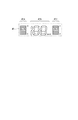
<VFD表示器41の構成>
VFD表示器41の外観の具体例を図3に示す。図3に示すように、VFD表示器41は、温度計表示部41a、速度計表示部41b、及び燃料計表示部41cを有している。温度計表示部41aは、自動車の冷却水温度を表示するために利用される。速度計表示部41bは、自動車の現在の車速を表示するために利用される。燃料計表示部41cは、燃料残量を表示するために利用される。
<Configuration of
A specific example of the appearance of the
温度計表示部41a、速度計表示部41b、及び燃料計表示部41cは、それぞれバーグラフや数値を表示できるように多数の表示セグメントで構成されている。多数の表示セグメントはそれぞれ独立して表示のオンオフを切り替えることができる。実際には、セグメント毎に独立したアノード(陽極)電極を有している。従って、各セグメントのアノード電極に印加する電圧のオンオフを切り替えることで、セグメント毎に表示のオンオフを制御することができる。
The
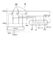
<電子制御装置(ECU)10の構成>
電子制御装置(ECU)10の構成例を図4に示す。この電子制御装置10は、図4に示すようにマイクロコンピュータ(CPU1)11、送信データ格納部12、中間バッファ13、及びプロトコル制御部14を備えている。
<Configuration of Electronic Control Unit (ECU) 10>
A configuration example of the electronic control unit (ECU) 10 is shown in FIG. As shown in FIG. 4, the
マイクロコンピュータ11は、予め組み込まれているプログラムを実行することにより、この装置を搭載した車両上で様々な情報、すなわち冷却水の温度、車速、燃料残量などの情報を収集して管理する。マイクロコンピュータ11が収集した情報は、他の装置に送信できるように送信データ格納部12上に順次に格納される。
The
送信データ格納部12を構成するメモリ(RAM)は、多数の送信データスロットで構成されている。送信データスロット毎に独立した情報が順番に格納される。プロトコル制御部14の2つの信号線CTX、CRXは、車載通信網CANと接続されている。一方の信号線CTXは、プロトコル制御部14が他の装置に対してデータを送信するために利用される。もう一方の信号線CRXは、プロトコル制御部14が他の装置からデータを受信するために利用される。
The memory (RAM) constituting the transmission
この車載通信網CANには、図1に示したように表示装置100が接続されている。従って、電子制御装置10は、車載通信網CANを介して、表示装置100との間でデータの送信及び受信を必要に応じてあるいは定期的に行うことができる。このデータ送受信の手順をプロトコル制御部14が管理する。例えば定期的に、あるいは表示装置100から要求があった時に、プロトコル制御部14は送信データ格納部12に格納されている情報を順番に取り出して、表示装置100に送信する。送信データ格納部12から取り出された情報は、一時的に中間バッファ13上に保持され、プロトコル制御部14の制御のタイミングに合わせて、中間バッファ13からプロトコル制御部14を経由して車載通信網CANに送出される。
A
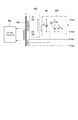
<VFD表示器41及びドライバ部42の電気回路の構成>
VFD表示器41及びドライバ部42の電気回路の構成例を図5に示す。VFD表示器41は、図5に示すように1つのカソード(陰極)電極と、グリッド電極と、多数のアノード電極とを有している。多数のアノード電極のそれぞれが表示要素のセグメントに対応している。各々のアノード電極に印加する電圧のオンオフを切り替えることにより、該当する位置のセグメントの表示のオンオフを制御することができる。
<Configuration of Electric Circuit of
An example of the configuration of the electric circuit of the
ドライバ部42は、ドライバの機能を有する集積回路42aと、セグメント毎に用意された多数のスイッチング回路42bとで構成されている。集積回路42aの入力に、主表示制御部20から出力される表示出力信号SG2が印加される。
The
集積回路42aは、入力される表示出力信号SG2をデコードして、各々のセグメントを制御するための制御信号を生成し、各々の制御信号を該当するセグメントのスイッチング回路42bに印加する。
The
各々のスイッチング回路42bは、VFD表示器41の該当するアノード電極に印加する電圧のオンオフを切り替える。ドライバ部42の電源ラインには、VFD電源43から電源電圧Vcc及びVEEが印加される。
Each switching
VFD表示器41のグリッド電極には、VFD電源43から電源電圧Vccが印加される。各スイッチング回路42bのスイッチングトランジスタのオンオフに応じて、VFD表示器41の各アノード電極には、電源電圧Vcc又はVEEに近い電圧が印加される。また、VFD表示器41のカソード電極に接続された2つの端子には、VFD電源43から電源電圧VK1及びVK2がそれぞれ印加される。
A power supply voltage Vcc is applied from the
<VFD電源43の構成>
VFD電源43の構成例を図6に示す。VFD電源43には、図6に示すようにDC−ACコンバータ43a、昇圧トランス43b、整流回路43c、及び平滑回路43dが備わっている。
<Configuration of
A configuration example of the
DC−ACコンバータ43aは、車両側の電源回路から供給される直流(DC)電圧(通常は12V)をスイッチングして交流(AC)の電圧を生成する。DC−ACコンバータ43aが生成した交流の電圧が昇圧トランス43bの一次側巻線に供給される。昇圧トランス43bの各二次側巻線には、一次側巻線との巻数比に応じて昇圧された交流電圧が誘起される。
The DC-
昇圧トランス43bの一方の二次側巻線に誘起される高電圧の交流電圧は、整流回路43cで整流され、平滑回路43dで平滑され、電源電圧Vcc及びVEEとして出力される。また、昇圧トランス43bのもう一方の二次側巻線に誘起される低電圧の交流電圧は、電源電圧VK1及びVK2として出力される。
The high AC voltage induced in one secondary winding of the step-up
<装置の動作>
図1に示した副表示制御部30の動作を図2に示す。すなわち、副表示制御部30のマイクロコンピュータ(CPU3)が所定のプログラムを実行することにより、図2に示す動作が実現される。図2に示す動作について以下に説明する。
<Operation of the device>
The operation of the sub
ステップS11では、副表示制御部30は、電子制御装置10が車載通信網CANに送信した表示情報(温度、車速、燃料残量)を、受信信号SG1として入力し、副表示制御部30の内部メモリ(RAM)に格納する。
In step S <b> 11, the sub
ステップS12では、副表示制御部30は、ステップS11で内部メモリに格納した表示情報に予め定めた変換処理を施すことにより、VFD表示部40用の「表示出力情報1」を生成する。すなわち、主表示制御部20が車載通信網CANから取得した情報に基づいて表示出力信号SG2を生成する動作と同等の動作を、副表示制御部30も実行することにより、副表示制御部30の内部で、表示出力信号SG2に相当する信号を「表示出力情報1」としてS12で生成する。
In step S12, the sub
実際には、受信信号SG1は温度、車速、燃料残量等を表す数値であるが、表示出力信号SG2は、VFD表示器41の各セグメントのオンオフを表す情報を予め定めた規則に従って順番に並べたシリアルデータ、あるいは複数ビットで構成されるパラレルデータとして符号化したデータである。従って、予め定めた規則に従って変換することにより、受信信号SG1の表示情報から表示出力信号SG2に相当する「表示出力情報1」を生成できる。
Actually, the received signal SG1 is a numerical value indicating temperature, vehicle speed, fuel remaining amount, etc., but the display output signal SG2 is arranged in order according to a predetermined rule, information indicating ON / OFF of each segment of the
ステップS13では、副表示制御部30はS12で生成したVFD表示部40用の「表示出力情報1」を、副表示制御部30の内部メモリ(RAM)に格納する。
In step S <b> 13, the sub
ステップS14では、副表示制御部30は、主表示制御部20が出力した表示出力信号SG2をフィードバック信号SG3としてフィードバック信号用入力ポート32から入力し、このフィードバック信号SG3を「表示出力情報2」として副表示制御部30の内部メモリ(RAM)に格納する。
In step S14, the sub
ステップS15では、副表示制御部30は、S13で格納した前記「表示出力情報1」と、S14で格納した前記「表示出力情報2」とを内部メモリから読み込んでこれらを全ビット(全セグメント)について比較する。
In step S15, the
S15の比較の結果、「表示出力情報1」と「表示出力情報2」の全ビットが一致した場合には、副表示制御部30の処理はS16からS11に戻り、一致しないビットを検出した場合には、副表示制御部30の処理はS16からS17に進む。
As a result of the comparison in S15, when all the bits of “display output information 1” and “display output information 2” match, the process of the sub
通常の状態であれば、主表示制御部20が車載通信網CANから取得した情報に基づいて表示出力信号SG2を生成する動作と、副表示制御部30が受信信号SG1から「表示出力情報1」を生成する動作とは同じになるので、「表示出力情報1」と「表示出力情報2」との比較の結果は全ビットが一致するはずである。しかし、例えば主表示制御部20の内部で回路の故障が発生した場合や、ノイズなどの影響で主表示制御部20の動作に異常が発生した場合や、主表示制御部20が実行するプログラム自体の不具合などによって、不一致が生じる可能性もある。この不一致が生じた状態は、本来表示すべき主表示制御部20が受信した表示情報(温度、車速、燃料残量)とは異なる情報がVFD表示器41側に表示出力信号SG2として印加される状態、すなわち異常な表示が行われる状態を意味する。このような異常な状態において、ステップS17以降の処理が実行される。
In the normal state, the main
ステップS17では、副表示制御部30は、制御信号SG4を出力して、主表示制御部20に対して特別な指示を与える。すなわち、VFD表示部40に対して表示出力信号SG2を出力する動作を停止するように、制御信号SG4で指示する。これにより、VFD表示器41の表示動作が停止する。
In step S <b> 17, the sub
ステップS18では、副表示制御部30は、主表示制御部20に与える制御信号SG4を制御して、異常の表示を行うように主表示制御部20に対して指示を与える。この指示により、主表示制御部20は、表示出力信号SG2を通常とは異なる状態に制御し、例えばVFD表示器41が異常の発生を表す点滅表示を行うように制御する。
In step S18, the sub
ステップS19では、副表示制御部30は、検出した異常の種類や発生した箇所などを表す故障情報を生成し、この情報を不揮発性メモリ25に書き込み記録する。
In step S <b> 19, the sub
<表示装置100の利点>
上述の表示装置100は、主表示制御部20の内部回路に故障が発生した場合や、ノイズの影響、あるいは主表示制御部20が実行するプログラム自体の不具合などを原因として、VFD表示器41の表示内容に異常が発生するような状況であっても、これらの異常を検出し自動的に対応することができる。すなわち、異常が発生すると、図2のステップS17で異常な表示を停止し、ステップS18で異常の発生を表示し、ステップS19で故障情報を故障情報を自動的に記録する。
<Advantages of
In the
<変形例>
図2に示した動作においては、「表示出力情報1」と「表示出力情報2」との比較の結果だけで故障の有無を識別している(S15、S16)が、その他の処理により故障の有無を識別することもできる。
<Modification>
In the operation shown in FIG. 2, the presence / absence of a failure is identified only by the comparison result between “display output information 1” and “display output information 2” (S15, S16). The presence or absence can also be identified.
例えば、主表示制御部20が定期的に車載通信網CANから表示情報(温度、車速、燃料残量)を受信するような場合には、図2に示したステップS11において、受信信号SG1が所定時間以上入力されない場合は、副表示制御部30が通信の異常とみなしてS17以降の処理を実行するように動作を変更することが考えられる。また、図2に示したステップS11において、受信信号SG1にエラー情報が含まれているような場合にも、副表示制御部30が通信の異常とみなしてS17以降の処理を実行するように動作を変更することが考えられる。
For example, when the main
また、ステップS19で記録する故障情報の内容については、図2に示したステップS11で検出した通信系の異常と、ステップS16で検出した主表示制御部20の故障とを区別できるようにそれぞれ独立したエラーコードを割り当てることが想定される。
Further, the contents of the failure information recorded in step S19 are independent so that the communication system abnormality detected in step S11 shown in FIG. 2 and the failure of the main
<補足説明>
(1)図1に示した表示装置100は、所定の通信経路(CAN)から入力される第1の表示指示情報に基づいて第2の表示指示情報(SG2)を生成する主表示制御部(20)と、前記主表示制御部から出力される前記第2の表示指示情報を入力して表示内容に反映する表示出力部(40)とを有する表示装置であり、この表示装置100は前記主表示制御部から独立した副表示制御部(30)を含む。
また、前記副表示制御部は、図2に示すように、前記通信経路から入力される前記第1の表示指示情報を、前記第2の表示指示情報(SG2)と同じ第3の表示指示情報に変換して記憶する表示指示情報変換部(S12,S13)と、前記第2の表示指示情報を前記主表示制御部の出力から入力して記憶する表示指示情報監視部(S14)と、前記表示指示情報監視部が記憶した前記第2の表示指示情報を前記表示指示情報変換部が記憶した前記第3の表示指示情報と比較し、少なくとも表示状態の異常の有無を識別する表示状態識別部(S15,S16)とを備えている。
<Supplementary explanation>
(1) The
Further, as shown in FIG. 2, the sub-display control unit converts the first display instruction information input from the communication path into third display instruction information that is the same as the second display instruction information (SG2). A display instruction information conversion unit (S12, S13) that converts and stores the second display instruction information from an output of the main display control unit and stores the second display instruction information; A display state identification unit that compares the second display instruction information stored in the display instruction information monitoring unit with the third display instruction information stored in the display instruction information conversion unit and identifies at least the presence or absence of an abnormality in the display state (S15, S16).
(2)また、前記表示状態識別部は、図2に示すように、表示状態の異常有を検出した場合に、前記主表示制御部もしくは前記表示出力部に対して表示動作を停止するための制御信号(SG4)を出力する(S17)。 (2) Further, as shown in FIG. 2, the display state identification unit is configured to stop the display operation with respect to the main display control unit or the display output unit when the display state abnormality is detected. A control signal (SG4) is output (S17).
(3)また、前記表示状態識別部は、図2に示すように、表示状態の異常有を検出した場合に、前記主表示制御部もしくは前記表示出力部に対して表示状態が異常であることを明示するための制御信号(SG4)を出力する(S18)。 (3) Further, as shown in FIG. 2, when the display state identification unit detects that the display state is abnormal, the display state is abnormal with respect to the main display control unit or the display output unit. Is output (S18).
(4)また、表示装置100は更に、不揮発性メモリ(25)を備え、前記表示状態識別部は、表示状態の異常有を検出した場合に、発生した異常の種類を表す故障情報を生成し、前記故障情報を前記不揮発性メモリ上に自動的に保存する(S19)。
(4) The
10 電子制御装置(ECU)
11 マイクロコンピュータ
12 送信データ格納部
13 中間バッファ
14 プロトコル制御部
20 主表示制御部
21 CANコントローラ
22 表示制御用出力ポート
25 不揮発性メモリ
30 副表示制御部
31 CANコントローラ
32 フィードバック信号用入力ポート
40 VFD表示部
41 VFD表示器
41a 温度計表示部
41b 速度計表示部
41c 燃料計表示部
42 ドライバ部
42a 集積回路
42b スイッチング回路
43 VFD電源
43a DC−ACコンバータ
43b 昇圧トランス
43c 整流回路
43d 平滑回路
100 表示装置
SG1 受信信号
SG2 表示出力信号
SG3 フィードバック信号
SG4 制御信号
10 Electronic control unit (ECU)
11
Claims (4)
前記主表示制御部から独立した副表示制御部を含み、
前記副表示制御部は、
前記通信経路から入力される前記第1の表示指示情報に対して前記変換処理と同じ変換処理を施すことにより第3の表示指示情報を生成して記憶する表示指示情報変換部と、
前記第2の表示指示情報を前記主表示制御部の出力から入力して記憶する表示指示情報監視部と、
前記表示指示情報監視部が記憶した前記第2の表示指示情報と前記表示指示情報変換部が記憶した前記第3の表示指示情報との比較結果に不一致が生じている状態の時に、前記主表示制御部の動作に異常が発生しているとみなすと共に、前記通信経路からの前記第1の表示指示情報の入力状況に基づいて通信の異常の有無を識別し、前記主表示制御部の異常又は前記通信の異常を検出した場合に、前記主表示制御部の異常及び前記通信の異常のうち発生した異常の種類を表す故障情報を生成する表示状態識別部と
を備えることを特徴とする表示装置。 A main display control unit that generates second display instruction information by performing predetermined conversion processing on the first display instruction information input from a predetermined communication path, and the main display control unit outputs the second display instruction information. A display device having a display output unit that inputs the second display instruction information and reflects it in display content,
A sub-display control unit independent of the main display control unit,
The sub-display control unit
A display instruction information conversion unit that generates and stores third display instruction information by performing the same conversion process as the conversion process on the first display instruction information input from the communication path;
A display instruction information monitoring unit for inputting and storing the second display instruction information from the output of the main display control unit;
The main display is in a state where there is a discrepancy in the comparison result between the second display instruction information stored in the display instruction information monitoring unit and the third display instruction information stored in the display instruction information conversion unit. together regarded as abnormal operation of the control unit occurs, the identifying the presence or absence of communication abnormality based on the input state of the first display instruction information from the communication path, abnormalities of the main display control unit or when detecting abnormalities of the communications, further comprising a display state identification unit for generating a failure information indicating the type of abnormality that occurs among the main display control unit anomalies and the communication abnormality Characteristic display device.
ことを特徴とする請求項1に記載の表示装置。 The display state identification unit, if the main abnormalities of the display control unit or detecting the abnormal of the communications, control to stop the display operation with respect to the main display control unit or the display output unit The display device according to claim 1, wherein a signal is output.
ことを特徴とする請求項1に記載の表示装置。 Said display state identification unit, the main anomalies display control unit or when detecting the abnormal of the communications, the display state with respect to the main display control unit or the display output unit is abnormal The display device according to claim 1, wherein a control signal for specifying is output.
前記表示状態識別部は、前記主表示制御部の異常又は前記通信の異常を検出した場合に、前記生成した故障情報を前記不揮発性メモリ上に自動的に保存する
ことを特徴とする請求項1に記載の表示装置。 In addition, a non-volatile memory is provided,
The display state identification unit, and wherein said main display control unit anomaly or of when detecting abnormalities of the communications, it automatically stores the failure information described above generated on the non-volatile memory The display device according to claim 1.
Priority Applications (1)
| Application Number | Priority Date | Filing Date | Title |
|---|---|---|---|
| JP2012159784A JP6118043B2 (en) | 2012-07-18 | 2012-07-18 | Display device |
Applications Claiming Priority (1)
| Application Number | Priority Date | Filing Date | Title |
|---|---|---|---|
| JP2012159784A JP6118043B2 (en) | 2012-07-18 | 2012-07-18 | Display device |
Publications (2)
| Publication Number | Publication Date |
|---|---|
| JP2014021275A JP2014021275A (en) | 2014-02-03 |
| JP6118043B2 true JP6118043B2 (en) | 2017-04-19 |
Family
ID=50196204
Family Applications (1)
| Application Number | Title | Priority Date | Filing Date |
|---|---|---|---|
| JP2012159784A Expired - Fee Related JP6118043B2 (en) | 2012-07-18 | 2012-07-18 | Display device |
Country Status (1)
| Country | Link |
|---|---|
| JP (1) | JP6118043B2 (en) |
Families Citing this family (6)
| Publication number | Priority date | Publication date | Assignee | Title |
|---|---|---|---|---|
| JP2014032292A (en) * | 2012-08-02 | 2014-02-20 | Yazaki Corp | Display device |
| JP7082471B2 (en) * | 2017-10-25 | 2022-06-08 | ローム株式会社 | Anomaly detection data recording device |
| JP2020106632A (en) | 2018-12-27 | 2020-07-09 | セイコーエプソン株式会社 | Liquid crystal device, electronic apparatus, and movable body |
| JP7271947B2 (en) | 2018-12-27 | 2023-05-12 | セイコーエプソン株式会社 | Liquid crystal drivers, electronic devices and moving bodies |
| JP7206953B2 (en) | 2019-01-28 | 2023-01-18 | セイコーエプソン株式会社 | Liquid crystal devices, liquid crystal drivers, electronic devices and moving bodies |
| CN114355648B (en) * | 2021-12-17 | 2024-04-12 | 山东蓝贝思特教装集团股份有限公司 | Liquid crystal writing device erasing voltage control system and method based on VFD driving chip |
Family Cites Families (12)
| Publication number | Priority date | Publication date | Assignee | Title |
|---|---|---|---|---|
| JPS6047596B2 (en) * | 1979-05-02 | 1985-10-22 | 東芝テック株式会社 | Electronic devices with display devices |
| JPS5843775B2 (en) * | 1979-08-29 | 1983-09-29 | 横河電機株式会社 | Processor backup system |
| JPS61151746A (en) * | 1984-12-26 | 1986-07-10 | Hitachi Ltd | Processing method of data error |
| JPH02189580A (en) * | 1989-01-18 | 1990-07-25 | Nec Corp | Display device |
| JP2670730B2 (en) * | 1992-10-02 | 1997-10-29 | エムケー精工株式会社 | Display device |
| DE19716197A1 (en) * | 1997-04-18 | 1998-10-22 | Itt Mfg Enterprises Inc | Microprocessor system for safety-critical regulations |
| JP3631702B2 (en) * | 2001-07-19 | 2005-03-23 | エヌイーシーシステムテクノロジー株式会社 | Drawing display system |
| JP2003091264A (en) * | 2001-09-17 | 2003-03-28 | Seiko Epson Corp | Inspection method and device |
| JP2005134655A (en) * | 2003-10-30 | 2005-05-26 | Toshiba Lsi System Support Kk | Driving circuit for liquid crystal display device, microcontrol unit mounted with driving circuit, and inspection method for the same |
| JP4277055B2 (en) * | 2007-05-29 | 2009-06-10 | シャープ株式会社 | Drive circuit, display device, and television system |
| US8117512B2 (en) * | 2008-02-06 | 2012-02-14 | Westinghouse Electric Company Llc | Failure detection and mitigation in logic circuits |
| JP5325032B2 (en) * | 2009-07-03 | 2013-10-23 | 株式会社日立製作所 | High reliability controller for multi-system |
-
2012
- 2012-07-18 JP JP2012159784A patent/JP6118043B2/en not_active Expired - Fee Related
Also Published As
| Publication number | Publication date |
|---|---|
| JP2014021275A (en) | 2014-02-03 |
Similar Documents
| Publication | Publication Date | Title |
|---|---|---|
| JP6046404B2 (en) | Display device | |
| JP6118043B2 (en) | Display device | |
| CN102431549A (en) | Electronic control apparatus for a vehicle | |
| TW201119173A (en) | Method of using power supply to execute remote monitoring of an electronic system | |
| US8621286B2 (en) | Fault information managing method and fault information managing program | |
| TWI488014B (en) | Control device | |
| JP4758276B2 (en) | Power supply system and system power supply | |
| KR101428288B1 (en) | Diagnosis method of side step apparatus for vehicle | |
| CN108399116A (en) | A kind of server power-up state monitoring system and method | |
| KR102066887B1 (en) | System for Motor Control Center having Redundant Protection Control Module | |
| JP2014032292A (en) | Display device | |
| JP2008143418A (en) | Data rewriting state display control device | |
| KR20170114827A (en) | Fail-safety circuit of smart power relay assembly | |
| JP2020078107A (en) | Motor control device | |
| CN108146494A (en) | The electronic control unit of EPS | |
| JP4747683B2 (en) | On-vehicle electronic control system, fault diagnosis method thereof, and on-vehicle electronic control device | |
| JP2015142452A (en) | Motor drive device | |
| KR101140177B1 (en) | Voltage sag management system | |
| JP6856416B2 (en) | Process control system | |
| JP4851498B2 (en) | Electric power steering control device | |
| KR101410870B1 (en) | Structure for Power Supplying for Cluster System of Construction Heavy Machine | |
| US20200278134A1 (en) | Electronic continuous-flow heater and method for operating such a heater | |
| JP2020035621A (en) | Hydrogen tank control device | |
| KR101545130B1 (en) | Device for forming a monitoring display of control system of power plant | |
| CN110778514B (en) | Fan control system |
Legal Events
| Date | Code | Title | Description |
|---|---|---|---|
| RD02 | Notification of acceptance of power of attorney |
Free format text: JAPANESE INTERMEDIATE CODE: A7422 Effective date: 20150122 |
|
| A621 | Written request for application examination |
Free format text: JAPANESE INTERMEDIATE CODE: A621 Effective date: 20150619 |
|
| A977 | Report on retrieval |
Free format text: JAPANESE INTERMEDIATE CODE: A971007 Effective date: 20160218 |
|
| A131 | Notification of reasons for refusal |
Free format text: JAPANESE INTERMEDIATE CODE: A131 Effective date: 20160301 |
|
| A521 | Request for written amendment filed |
Free format text: JAPANESE INTERMEDIATE CODE: A523 Effective date: 20160329 |
|
| A131 | Notification of reasons for refusal |
Free format text: JAPANESE INTERMEDIATE CODE: A131 Effective date: 20160830 |
|
| A521 | Request for written amendment filed |
Free format text: JAPANESE INTERMEDIATE CODE: A523 Effective date: 20160930 |
|
| TRDD | Decision of grant or rejection written | ||
| A01 | Written decision to grant a patent or to grant a registration (utility model) |
Free format text: JAPANESE INTERMEDIATE CODE: A01 Effective date: 20170228 |
|
| A61 | First payment of annual fees (during grant procedure) |
Free format text: JAPANESE INTERMEDIATE CODE: A61 Effective date: 20170324 |
|
| R150 | Certificate of patent or registration of utility model |
Ref document number: 6118043 Country of ref document: JP Free format text: JAPANESE INTERMEDIATE CODE: R150 |
|
| R250 | Receipt of annual fees |
Free format text: JAPANESE INTERMEDIATE CODE: R250 |
|
| R250 | Receipt of annual fees |
Free format text: JAPANESE INTERMEDIATE CODE: R250 |
|
| R250 | Receipt of annual fees |
Free format text: JAPANESE INTERMEDIATE CODE: R250 |
|
| LAPS | Cancellation because of no payment of annual fees |