JP6095350B2 - Imaging apparatus and defective pixel detection method - Google Patents
Imaging apparatus and defective pixel detection method Download PDFInfo
- Publication number
- JP6095350B2 JP6095350B2 JP2012270261A JP2012270261A JP6095350B2 JP 6095350 B2 JP6095350 B2 JP 6095350B2 JP 2012270261 A JP2012270261 A JP 2012270261A JP 2012270261 A JP2012270261 A JP 2012270261A JP 6095350 B2 JP6095350 B2 JP 6095350B2
- Authority
- JP
- Japan
- Prior art keywords
- defective pixel
- solid
- image
- imaging device
- address
- Prior art date
- Legal status (The legal status is an assumption and is not a legal conclusion. Google has not performed a legal analysis and makes no representation as to the accuracy of the status listed.)
- Active
Links
Images


Description
本発明は、撮像装置に関し、特に、撮像装置に用いられる固体撮像素子の欠陥画素を検出する技術に関する。 The present invention relates to an imaging apparatus, and more particularly to a technique for detecting defective pixels of a solid-state imaging element used in the imaging apparatus.
CMOSセンサ等の固体撮像素子の小型化が進むにつれて、欠陥画素の発生頻度が上がっており、種々の異なる特性を有する欠陥画素が確認されている。代表的な欠陥画素としては、遮光時のようなダーク画像で白点となる白点欠陥画素や、ライトボックスのような高輝度被写体撮影時に黒点となる黒点欠陥画素が挙げられるが、電荷蓄積時間や温度によって出力レベルが変化する特性を持つ欠陥画素も知られている。 As solid-state imaging devices such as CMOS sensors are miniaturized, the frequency of defective pixels increases, and defective pixels having various different characteristics have been confirmed. Typical defective pixels include white point defective pixels that become white points in dark images when light is blocked, and black point defective pixels that become black points when shooting high-luminance subjects such as light boxes. There are also known defective pixels whose output level changes with temperature.
このような欠陥画素に対処するために、撮像装置では、例えば、生産ラインで固体撮像素子の欠陥画素検出を行い、検出したアドレスを不揮発性メモリに記憶し、そのアドレスに基づいて欠陥画素の周辺画素から欠陥画素を補正する補間画素を作成している。また、欠陥画素検出技術として、白点欠陥画素を検出する際には低輝度被写体で、黒点欠陥画素を検出する際には高輝度被写体で欠陥画素検出を行うことにより、検出漏れや誤検出を低減させる技術が提案されている(特許文献1参照)。更に、温度に応じて欠陥画素を検出する閾値を変化させて、検出性能の温度に対する依存性を低減することにより、誤検出を低減させる技術が提案されている(特許文献2参照)。 In order to deal with such defective pixels, the imaging device, for example, detects a defective pixel of a solid-state imaging device on a production line, stores the detected address in a nonvolatile memory, and around the defective pixel based on the address An interpolation pixel for correcting a defective pixel from the pixel is created. In addition, as a defective pixel detection technique, detection of defective pixels or false detections is performed by detecting defective pixels with a low-intensity subject when detecting white-point defective pixels and with a high-luminance subject when detecting black-point defective pixels. A technique for reducing the thickness has been proposed (see Patent Document 1). Furthermore, a technique has been proposed in which false detection is reduced by changing a threshold value for detecting a defective pixel in accordance with temperature to reduce dependency of detection performance on temperature (see Patent Document 2).
ここで、CMOSセンサにおける欠陥画素の例について説明する。図7は、CMOSセンサの欠陥画素における温度と出力特性との関係の例を示す図である。図7(a)は電荷蓄積時間を1/60秒(TV60)としたときの、図7(b)は電荷蓄積時間を1/2秒(TV2)としたときの、欠陥画素α,β,γの温度と出力特性との関係を示している。 Here, an example of defective pixels in the CMOS sensor will be described. FIG. 7 is a diagram illustrating an example of a relationship between temperature and output characteristics in a defective pixel of a CMOS sensor. 7A shows the defective pixels α, β, when the charge accumulation time is 1/60 seconds (TV60), and FIG. 7B shows the charge accumulation time when the charge accumulation time is 1/2 seconds (TV2). The relationship between the temperature of γ and the output characteristics is shown.
図7(a),(b)を対比すると明らかなように、欠陥画素αは、一般的に知られている特性を示す白点欠陥画素であって、CMOSセンサの温度によって出力レベルが変化すると共に、電荷蓄積時間に依存して出力レベルが変化する欠陥画素である。欠陥画素βは、温度によって出力レベルが変化するが、電荷蓄積時間による出力レベルの変化は殆どないものである。欠陥画素γは、温度にも電荷蓄積時間にもよらず、出力レベルが一定の画素である。欠陥画素α,βはフォトダイオード(PD)の欠陥で現れる特性であり、欠陥画素γはフローティングディフュージョン(FD)の欠陥で現れる特性である。 As is clear from the comparison between FIGS. 7A and 7B, the defective pixel α is a white point defective pixel having a generally known characteristic, and its output level changes depending on the temperature of the CMOS sensor. At the same time, it is a defective pixel whose output level changes depending on the charge accumulation time. The defective pixel β has an output level that changes with temperature, but has almost no change in output level due to the charge accumulation time. The defective pixel γ is a pixel having a constant output level regardless of the temperature and the charge accumulation time. The defective pixels α and β are characteristics that appear due to defects in the photodiode (PD), and the defective pixel γ is a characteristic that appears as defects in the floating diffusion (FD).
欠陥画素を検知可能な出力レベルを100mVと仮定すると、全ての白点欠陥画素を精度よく検出するためには、図7から、TV60ではCMOSセンサが60℃以上に、TV2ではCMOSセンサが55℃以上になった状態で検出を行う必要のあることがわかる。
Assuming that the output level at which defective pixels can be detected is 100 mV, in order to accurately detect all white point defective pixels, from FIG. 7, the
しかしながら、撮像装置の生産性を確保するためには、欠陥画素検出に必要以上に時間をかけるわけにはいかないため、固体撮像素子が低温の状態で欠陥画素検出を行う必要がある。低温状態で出力特性が温度により変化する欠陥画素を検出するためには、上記特許文献2のように検出閾値を低く設定することとなるが、検出閾値を下げすぎると、本来検知不要な欠陥画素γの特性を持つ欠陥画素が大量に検出されてしまうという問題が生じる。また、これにより、必要以上に欠陥画素を補間する補正を行うことにより、補正後の出力画像が劣化してしまうという問題が生じる。 However, in order to ensure the productivity of the imaging apparatus, it is not possible to spend more time than necessary to detect defective pixels, and therefore it is necessary to detect defective pixels while the solid-state imaging device is at a low temperature. In order to detect defective pixels whose output characteristics change depending on temperature in a low temperature state, the detection threshold is set low as in Patent Document 2 described above. However, if the detection threshold is too low, defective pixels that are not originally required to be detected are detected. There arises a problem that a large number of defective pixels having the γ characteristic are detected. This also causes a problem that the corrected output image is deteriorated by performing correction for interpolating defective pixels more than necessary.
これに対して、TV2の状態として検出閾値を高く設定することで、欠陥画素γの特性を持つ欠陥画素を大量に検出することなく、欠陥画素αのみを検出することができる。また、欠陥画素γに対しては、欠陥画素α,βとは異なり、PD電荷転送をオフ(OFF)とした状態でも検出が可能である特性を利用して、別途に検出することで対応が可能である。このような方法により、必要以上に補正を行うことで補正後の出力画像を劣化させてしまう上記問題の発生を防ぐことができるが、固体撮像素子が低温状態では欠陥画素βを検出することができないという問題が残る。 On the other hand, by setting the detection threshold high as the state of the TV 2, it is possible to detect only the defective pixel α without detecting a large amount of defective pixels having the characteristic of the defective pixel γ. Further, unlike the defective pixels α and β, the defective pixel γ can be dealt with by detecting it separately using a characteristic that can be detected even when the PD charge transfer is turned off. Is possible. Such a method can prevent occurrence of the above-described problem that the output image after correction is deteriorated by performing correction more than necessary, but the solid-state imaging device may detect the defective pixel β in a low temperature state. The problem of being unable to remain remains.
本発明は、固体撮像素子が低温の状態でも、出力特性が温度に依存するが電荷蓄積時間には殆ど依存しない特性を持つ欠陥画素の検出精度を高める技術を提供することを目的とする。 An object of the present invention is to provide a technique for improving the detection accuracy of a defective pixel having a characteristic that the output characteristic depends on the temperature but hardly depends on the charge accumulation time even when the solid-state imaging device is in a low temperature state.
本発明に係る撮像装置は、固体撮像素子が有する欠陥画素を、前記固体撮像素子によって得られた画像から検出する検出手段と、前記固体撮像素子によって得られた第1の画像から前記検出手段が検出した欠陥画素のアドレスから、前記固体撮像素子によって得られた第2の画像から前記検出手段が検出した欠陥画素のアドレスを除去して、所定の特性の欠陥画素のアドレスを得る除去手段とを備え、前記第1の画像は、前記固体撮像素子のフォトダイオードの電荷を転送して得られた画像であり、前記第2の画像は、前記固体撮像素子のフォトダイオードの電荷を転送せずに得られた画像であることを特徴とする。 The image pickup apparatus according to the present invention includes: a detection unit that detects a defective pixel included in a solid-state image sensor from an image obtained by the solid-state image sensor; and the detection unit that detects a first image obtained by the solid-state image sensor. Removing means for removing the address of the defective pixel detected by the detecting means from the second image obtained by the solid-state imaging device from the detected address of the defective pixel, and obtaining the address of the defective pixel having a predetermined characteristic; The first image is an image obtained by transferring the charge of the photodiode of the solid-state imaging device, and the second image is transferred without transferring the charge of the photodiode of the solid-state imaging device. It is an obtained image .
本発明に係る別の撮像装置は、固体撮像素子によって得られた第1の画像から、前記固体撮像素子によって得られた第2の画像を減算して差分画像を得る減算手段と、前記減算手段により得られた前記差分画像から、前記固体撮像素子が有する所定の特性の欠陥画素のアドレスを検出する検出手段と、を備え、前記検出手段は、前記固体撮像素子が所定の温度より高いときには前記第1の画像から欠陥画素のアドレスを検出し、該検出した欠陥画素のアドレスを前記所定の特性の欠陥画素のアドレスとすることを特徴とする。 Another imaging apparatus according to the present invention includes a subtracting unit that subtracts a second image obtained by the solid-state imaging device from a first image obtained by the solid-state imaging device, and obtains a difference image; and the subtracting unit Detecting means for detecting an address of a defective pixel having a predetermined characteristic possessed by the solid-state imaging device from the difference image obtained by the step , and when the solid-state imaging device is higher than a predetermined temperature, the detecting means A defective pixel address is detected from the first image, and the detected defective pixel address is used as the defective pixel address having the predetermined characteristic .
本発明によれば、撮像素子が低温の状態でも、出力特性が温度に依存するが電荷蓄積時間には殆ど依存しない特性を持つ欠陥画素を精度よく検出することができる。これにより不必要な欠陥画素の補間を行うことがなくなるために、品質の高い出力画像を得ることができる。 According to the present invention, even when the image sensor is in a low temperature state, it is possible to accurately detect a defective pixel having a characteristic whose output characteristic depends on temperature but hardly depends on the charge accumulation time. Accordingly, unnecessary defective pixel interpolation is not performed, so that a high-quality output image can be obtained.
以下、本発明の実施の形態について、添付図面を参照して詳細に説明する。ここでは、本発明に係る欠陥画素検出方法を採用した撮像装置の一例としてデジタルビデオカメラを取り上げて、本発明を説明することとする。 Hereinafter, embodiments of the present invention will be described in detail with reference to the accompanying drawings. Here, the present invention will be described by taking a digital video camera as an example of an imaging apparatus employing the defective pixel detection method according to the present invention.
<デジタルビデオカメラの外観構造>
図1は、本発明の実施の形態に係るデジタルビデオカメラの外観構造を示す斜視図である。デジタルビデオカメラ100は、撮像画像、撮像条件、デジタルビデオカメラ100の機能設定や動作設定等の各種情報を表示する表示部として、液晶(LCD)パネル101及びファインダ102を備える。また、デジタルビデオカメラ100は、電源ケーブル(不図示)を接続するためのコネクタ105を備える。デジタルビデオカメラ100は、装着されたバッテリ(不図示)からの給電を受けて動作し、そのバッテリはバッテリ収納部106の内側に収容されている。
<Appearance structure of digital video camera>
FIG. 1 is a perspective view showing an external structure of a digital video camera according to an embodiment of the present invention. The
デジタルビデオカメラ100は、ユーザからの各種操作を受け付ける各種スイッチ、ボタン、タッチパネル等の操作部材からなる操作部107を備える。液晶パネル101に表示されるメニューボタンや種々の機能アイコンを選択してタッチ操作を行うことにより、選択した機能の実行が可能となっている。機能アイコンとしては、例えば、終了ボタン、戻るボタン、画像送りボタン、ジャンプボタン、絞込みボタン、属性変更ボタン等が挙げられる。なお、タッチパネルは、液晶パネル101に重畳配置されている。タッチパネルのタッチ検出方法には制限はなく、例えば、抵抗膜方式、静電容量方式、表面弾性波方式、赤外線方式、電磁誘導方式、画像認識方式、光センサ方式等が挙げられる。
The
また、デジタルビデオカメラ100は、トリガボタン103と、モード切替スイッチ104と、ズームキー108と、電源スイッチ109とを備える。トリガボタン103は、撮影指示(撮影開始/撮影終了)を行う。モード切替スイッチ104は、動作モード(動画撮影モード/静止画撮影モード)の切り替えを行う。また、モード切替スイッチ104は、撮影モード(オート撮影モード、オートシーン判別モード、マニュアルモード、撮影シーン別のシーンモード、プログラムAEモード、カスタムモード等)の切り替えを行う。ズームキー108は、光学ズームや電子ズーム等のズーム操作を行う。電源スイッチ109は、電源のオン(ON)/オフ(OFF)を切り替える。
The
デジタルビデオカメラ100には、メモリカード等の記録媒体220(図2参照)を格納するための記録媒体スロット111を備え、記録媒体スロット111は蓋112により開閉自在となっている。記録媒体スロット111に格納された記録媒体220は、デジタルビデオカメラ100の本体と通信可能となる。デジタルビデオカメラ100は、撮影時にデジタルビデオカメラ100とユーザの手を固定するためのグリップベルト110を備える。
The
<デジタルビデオカメラのハードウエア構成>
図2は、デジタルビデオカメラ100の概略のハードウエア構成を示すブロック図である。なお、図2において、図1と同じ構成要素について同じ符号を示している。デジタルビデオカメラ100は、バリア201、撮影レンズ202、シャッタ203、撮像素子204、A/D変換部205、画像処理部206、メモリ制御部207、D/A変換部208、メモリ209及びシステム制御部210を備える。
<Digital video camera hardware configuration>
FIG. 2 is a block diagram showing a schematic hardware configuration of the
バリア201は、撮影レンズ202を覆うことにより、撮影レンズ202やシャッタ203、撮像素子204を含む撮像光学系の汚れや破損を防止する。撮影レンズ202は、ズームレンズやフォーカスレンズを含むレンズ群である。シャッタ203は、絞り機能を備え、撮像素子204に対する露光量を制御する。撮像素子204は、被写体の光学像を電気信号(アナログ信号)に変換するMOSセンサやCCDセンサ等の固体撮像素子である。A/D変換部205は、撮像素子204から出力されるアナログ信号をデジタル信号(画像データ)に変換する。
The
画像処理部206は、A/D変換部205から出力される画像データ又はメモリ制御部207から受信する画像データに対して、画素補間処理や縮小等のリサイズ処理、色変換処理等を行う。また、画像処理部206は、システム制御部210が露光制御や測距制御を行う際に用いるデータを、撮影した画像データを用いて所定の演算処理を行うことにより求める。なお、システム制御部210が実行する露光制御や測距制御としては、TTL(スルー・ザ・レンズ)方式のAF(オートフォーカス)処理、TTL方式のAWB(オートホワイトバランス)処理、AE(自動露出)処理、EF(フラッシュプリ発光)処理等が挙げられる。
The
A/D変換部205から出力されるデジタル信号(画像データ)は、画像処理部206とメモリ制御部207を介して、或いは、メモリ制御部207を介して、メモリ209に書き込まれる。また、メモリ209は、画像表示用のメモリ(ビデオメモリ)を兼ねており、液晶パネル101及びファインダ102に表示するための画像表示用データを格納する。なお、メモリ209は、所定枚数の静止画像、所定時間の動画像及び音声データを格納するのに十分な記憶容量を備えている。D/A変換部208は、メモリ209に格納されている画像表示用データをアナログ信号に変換して液晶パネル101やファインダ102に供給し、これにより、液晶パネル101やファインダ102に画像等が表示される。なお、A/D変換部205によりA/D変換されてメモリ209に蓄積された画像データをD/A変換部208でD/A変換し、液晶パネル101とファインダ102に逐次転送することにより、電子ビューファインダ機能によるスルー画像表示を行うことができる。
A digital signal (image data) output from the A /
デジタルビデオカメラの100は、不揮発性メモリ211、システムメモリ212、システムタイマ213、電源制御部214、電源部215及び記録媒体I/F216を備える。不揮発性メモリ211は、電気的に消去/記録が可能なメモリであり、例えば、EEPROM等が用いられる。不揮発性メモリ211は、システム制御部210の動作用の定数、プログラム(後述する図3及び図5のフローチャートを実行するためのプログラムを含む)を記憶している。
The
システム制御部210は、デジタルビデオカメラ100の全体的な制御を行い、シャッタ203の操作による撮像素子204からの信号読み出しから記録媒体220に画像データを書き込むまでの、一連の撮影処理の動作を開始する。また、システム制御部210は、不揮発性メモリ211に記憶された所定のプログラムを実行することにより、後述する各種の処理を実行する。更に、システム制御部210は、メモリ209、D/A変換部208、液晶パネル101及びファインダ102等を制御することにより液晶パネル101及びファインダ102の表示制御を行う。
The
システムメモリ212には、RAMが用いられ、システム制御部210の動作用の定数や変数が一時的に記憶され、また、不揮発性メモリ211から読み出したプログラム等が展開される。システムタイマ213は、各種の制御に用いる時間や内蔵された時計の時間を計測する。トリガボタン103、モード切替スイッチ104、操作部107、電源スイッチ109は、図1を参照して既に説明しているため、ここでの説明を省略する。
The
電源部215は、アルカリ電池やリチウム電池等の一次電池やNiCd電池やNiMH電池、Li電池等の二次電池、ACアダプター等である。電源制御部214は、電池検出回路、DC−DCコンバータ、通電するブロックを切り替えるスイッチ回路等により構成され、電源部215における電池の装着の有無や電池の種類、電池残量の検出を行う。また、電源制御部214は、検出結果とシステム制御部210からの指示に基づいてDC−DCコンバータを制御し、必要な電圧を必要な期間、記録媒体220を含む各部へ供給する。記録媒体I/F216は、記録媒体220とシステム制御部210との通信を可能にするインタフェースである。記録媒体220は、例えば、メモリカード等の半導体メモリ、ハードディスク、光ディスク等である。
The
<撮像素子204の欠陥画素検出処理>
次に、撮像素子204の欠陥画素検出処理について説明する。以下の説明では、先に説明した図7と同様に、撮像素子204の温度と電荷蓄積時間によって出力特性(出力レベル)が変化する(出力レベルの温度依存性と電荷蓄積時間依存性とがある)白点欠陥画素を欠陥画素αとする。また撮像素子204の温度によって出力レベルが変化するが、電荷蓄積時間による出力レベルの変化は殆どない(出力レベルに温度依存性はあるが電荷蓄積時間依存性は殆どない)白点欠陥画素を欠陥画素βとする。更に、撮像素子204の温度にも電荷蓄積時間にもよらず、出力レベルが一定である(出力レベルの温度依存性と電荷蓄積時間依存性とがない)白点欠陥画素を欠陥画素γとする。したがって、欠陥画素α,βは、フォトダイオード(PD)の欠陥で現れ、欠陥画素γはフローティングディフュージョン(FD)の欠陥で現れる。なお、撮像素子204がいかなる温度であったとしても欠陥画素α,βの取得を可能とするために、欠陥画素検出に用いる閾値は、撮像素子204の温度に応じて変化させるものとする。
<Defective Pixel Detection Processing of
Next, the defective pixel detection process of the
[第1の欠陥画素検出方法]
第1の欠陥画素検出方法では、複数の検出条件で検出された全ての欠陥画素から、任意の検出条件で検出された欠陥画素を排除することで、欠陥画素を検出する。図3は、第1の欠陥画素検出方法の処理手順を示すフローチャートである。なお、システム制御部210が不揮発性メモリ211に記憶された所定のプログラムを読み出してシステムメモリ212のワークエリアに展開、実行してデジタルビデオカメラ100の各部を制御することにより、図3のフローチャートの各処理が実行される。
[First defective pixel detection method]
In the first defective pixel detection method, a defective pixel is detected by excluding a defective pixel detected under an arbitrary detection condition from all defective pixels detected under a plurality of detection conditions. FIG. 3 is a flowchart showing a processing procedure of the first defective pixel detection method. The
先ず、ステップS301では、システム制御部210は、ダーク画像を撮像するための前準備として、シャッタ203やレンズキャップ等の構成要素を使用して遮光を行い、電荷蓄積時間を短秒露光に設定する電荷蓄積制御を行う。ここでは、短秒露光の電荷蓄積時間を1/60秒(TV60)とする。続くステップS302では、システム制御部210は、ステップS301で遮光された短秒蓄積のダーク画像である撮像画像A_in(第1の撮像画像)を取得する。続いて、ステップS303では、システム制御部210は、ステップS302で取得した撮像画像A_inを用いて欠陥画素検出(第1の検出ステップ)を行う。
First, in step S301, as a preparation for capturing a dark image, the
次に、ステップS304では、システム制御部210は、ステップS303で欠陥画素検出を行った結果として得られた欠陥画素検出結果A_outを取得する。ここで得られる欠陥画素は、欠陥画素α,β,γの全てである。そして、ステップS305において、システム制御部210は、PD電荷転送をオフに設定する。これにより、PDの欠陥である欠陥画素α,βは発生せず、FDの欠陥である欠陥画素γのみが発生する状態になる。なお、PD電荷転送をオフにする代わりに、電荷蓄積状態に設定してもよい。
Next, in step S304, the
次のステップS306では、システム制御部210は、ステップS305でPD電荷転送がオフに設定された状態で、短秒蓄積のダーク画像である撮像画像B_in(第2の撮像画像)を取得する。そして、続くステップS307では、システム制御部210は、ステップS306で取得した撮像画像B_inを用いて欠陥画素検出(第2の検出ステップ)を行う。続いて、ステップS308では、システム制御部210は、ステップS307で欠陥画素検出を行った結果として得られた欠陥画素検出結果B_outを取得する。ここで得られる欠陥画素は、ステップS304で得られた欠陥画素検出結果A_outに存在する欠陥画素γと同等である。
In the next step S306, the
そこで、次のステップS309では、システム制御部210は、ステップS304で得られた欠陥画素検出結果A_outからステップS308で得られた欠陥画素検出結果B_outを除去することにより、欠陥画素検出結果C_outを取得する。この欠陥画素検出結果C_outは欠陥画素α,βのみを検出している。つまり、欠陥画素検出結果C_outから欠陥画素α,βが決定される。これにより、本処理は終了となる。
Therefore, in the next step S309, the
以上の処理の通り、第1の欠陥画素検出方法では、複数の検出条件で検出された全ての欠陥画素から任意の検出条件で検出された欠陥画素を排除する。これにより、出力レベルの温度依存性はあるが、電荷蓄積時間依存性が殆どない特性を有する欠陥画素βに対して、撮像素子204が低温の状態でも、誤検出の発生を低減した精度の高い検出を行うことが可能となる。
As described above, in the first defective pixel detection method, defective pixels detected under an arbitrary detection condition are excluded from all defective pixels detected under a plurality of detection conditions. As a result, with respect to the defective pixel β having the characteristic that the output level is temperature-dependent but has almost no charge accumulation time dependency, the occurrence of false detection is reduced even when the
また、第1の欠陥画素検出方法では、欠陥画素検出に用いる閾値を撮像素子204の温度に応じて変化させているため、撮像素子204の温度が高温になった場合でも、欠陥画素検出が可能である。即ち、欠陥画素γは、従来と同様にPD電荷転送をオフとした状態で検出可能である。そこで、この特性を利用して、欠陥画素γのみを検出し、ステップS309の検出結果と欠陥画素γのみの検出結果とをOR処理することで、より高い精度で欠陥画素α,β,γの全てを検出することができる。
Further, in the first defective pixel detection method, the threshold used for detecting defective pixels is changed according to the temperature of the
なお、撮像素子204が高温状態にある場合には、欠陥画素検出に用いる閾値が充分に高い値となるために、欠陥画素γの誤検出の発生がなくなる。そのため、撮像素子204の温度が所定の温度を超えた場合には、ステップS305以降の処理を省略することにより、欠陥画素検出処理時間の短縮を図ってもよい。第1の欠陥画素検出方法により得られた欠陥画素の画素値を周囲の画素を用いて補間することにより、欠陥画素の補正が可能となることは言うまでもない。
When the
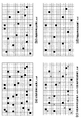
図4は、第1の欠陥画素検出方法を実行した場合に、欠陥画素検出結果がどのように遷移するかを模式的示す図である。図4(a)は、ステップS304で得られた欠陥画素検出結果A_outのイメージ図である。黒四角(■)は、検出された欠陥画素を示しており、ここに示される欠陥画素は、欠陥画素α,β,γの全てである。図4(b)は、ステップS308で得られた欠陥画素検出結果B_outのイメージ図であり、ここに示される欠陥画素は欠陥画素γのみである。 FIG. 4 is a diagram schematically showing how the defective pixel detection result transitions when the first defective pixel detection method is executed. FIG. 4A is an image diagram of the defective pixel detection result A_out obtained in step S304. Black squares (■) indicate detected defective pixels, and the defective pixels shown here are all defective pixels α, β, and γ. FIG. 4B is an image diagram of the defective pixel detection result B_out obtained in step S308, and the defective pixels shown here are only defective pixels γ.
図4(c)は、ステップS309で実施している処理のイメージ図である。ここでは、ステップS304で得られた欠陥画素検出結果A_outからステップS308で得られた欠陥画素検出結果B_outを除去しており、バツ印(×)が除去される欠陥画素を示している。図4(d)は、ステップS309で得られた欠陥画素検出結果C_outのイメージ図であり、ここに示される欠陥画素は欠陥画素α,βのみとなる。 FIG. 4C is an image diagram of the processing performed in step S309. Here, the defective pixel detection result B_out obtained in step S308 is removed from the defective pixel detection result A_out obtained in step S304, and a defective pixel from which the cross (x) is removed is shown. FIG. 4D is an image diagram of the defective pixel detection result C_out obtained in step S309, and the defective pixels shown here are only defective pixels α and β.
[第2の欠陥画素検出方法]
第2の欠陥画素検出方法では、第1の撮像画像(任意の撮影画像)から、第1の撮像画像とは異なる第2の撮像画像(別の任意の撮影画像)を減算することによって得られた画像データを用いて、欠陥画素を検出する。図5は、第2の欠陥画素検出方法の処理手順を示すフローチャートである。なお、システム制御部210が不揮発性メモリ211に記憶された所定のプログラムを読み出してシステムメモリ212のワークエリアに展開、実行してデジタルビデオカメラ100の各部を制御することにより、図5のフローチャートの各処理が実行される。
[Second defective pixel detection method]
In the second defective pixel detection method, it is obtained by subtracting a second captured image (another arbitrary captured image) different from the first captured image from the first captured image (arbitrary captured image). The defective pixel is detected using the obtained image data. FIG. 5 is a flowchart showing a processing procedure of the second defective pixel detection method. The
先ず、ステップS501では、システム制御部210は、ダーク画像を撮像するための前準備として、シャッタ203やレンズキャップ等の構成要素を使用して遮光を行い、電荷蓄積時間を短秒露光に設定する。ここでも、短秒露光の電荷蓄積時間を1/60秒(TV60)とする。続くステップS502では、システム制御部210は、ステップS501で遮光された短秒蓄積のダーク画像である撮像画像A_inを取得する。続くステップS503では、システム制御部210は、PD電荷転送をオフに設定する。これにより、PDの欠陥である欠陥画素α,βは発生せず、FDの欠陥である欠陥画素γのみが発生する状態になる。なお、PD電荷転送をオフにする代わりに、電荷蓄積状態に設定してもよい。
First, in step S501, as a preparation for capturing a dark image, the
次に、ステップS504では、システム制御部210は、ステップS503でPD電荷転送がオフに設定された状態で、短秒蓄積のダーク画像である撮像画像B_inを取得する。続くステップS505では、システム制御部210は、ステップS502で得られた撮像画像A_inからステップS504で得られた撮像画像B_inを減算し、これにより、差分画像C_inを取得する。続いて、ステップS506では、システム制御部210は、ステップS505で取得した差分画像C_inに対して欠陥画素検出を行う。そして、ステップS507では、システム制御部210は、ステップS506で欠陥画素検出を行った結果として得られた欠陥画素検出結果C_outを取得する。この欠陥画素検出結果C_outは、欠陥画素α,βのみを検出しており、これにより、本処理は終了となる。
Next, in step S504, the
以上の処理の通り、第2の欠陥画素検出方法では、任意の撮像画像A_inから撮像画像A_inとは異なる任意の撮像画像B_inを減算することによって得られた差分画像C_inに対して欠陥画素検出を行う。これにより、出力レベルの温度依存性はあるが、電荷蓄積時間依存性が殆どない特性を有する欠陥画素βに対して、撮像素子204が低温の状態でも、誤検出の発生を低減した精度の高い検出を行うことが可能となる。
As described above, in the second defective pixel detection method, defective pixel detection is performed on the difference image C_in obtained by subtracting an arbitrary captured image B_in different from the captured image A_in from an arbitrary captured image A_in. Do. As a result, with respect to the defective pixel β having the characteristic that the output level is temperature-dependent but has almost no charge accumulation time dependency, the occurrence of false detection is reduced even when the
また、第2の欠陥画素検出方法では、欠陥画素検出に用いる閾値を撮像素子204の温度に応じて変化させているため、撮像素子204の温度が高温になった場合でも、欠陥画素検出が可能である。即ち、欠陥画素γは、従来と同様にPD電荷転送をオフとした状態で検出可能である。そこで、この特性を利用して、欠陥画素γのみを検出し、ステップS309の検出結果と欠陥画素γのみの検出結果とをOR処理することで、より高い精度で欠陥画素α,β,γの全てを検出することができる。
In the second defective pixel detection method, the threshold used for detecting defective pixels is changed in accordance with the temperature of the
なお、撮像素子204が高温状態にある場合には、欠陥画素検出に用いる閾値が充分に高い値となるために、欠陥画素γの誤検出の発生がなくなる。そのため、撮像素子204の温度が所定の温度を超えた場合には、ステップS503からステップS505の処理を省略することにより、欠陥画素検出処理時間の短縮を図ってもよい。第2の欠陥画素検出方法により得られた欠陥画素を周囲の画素を用いて補間することにより、欠陥画素の補正が可能となることは言うまでもない。
When the
図6は、第2の欠陥画素検出方法を実行した場合に、欠陥画素検出結果がどのように遷移するかを模式的示す図であり、図6(a)に示すように、図6(b)〜(e)は、撮像素子204の撮像領域の任意の水平ラインを抽出した際の画素と出力レベルの関係を示している。
FIG. 6 is a diagram schematically showing how the defective pixel detection result transitions when the second defective pixel detection method is executed. As shown in FIG. 6A, FIG. (E) to (e) show the relationship between pixels and output levels when an arbitrary horizontal line in the imaging region of the
図6(b)は、ステップS502で得られた撮像画像A_inのイメージ図であり、ここで得られた欠陥画素は欠陥画素α,β,γの全てである。図6(c)は、ステップS504で得られた撮像画像B_inのイメージ図であり、ここで得られた欠陥画素は欠陥画素γのみである。図6(d)は、ステップS505で実施している処理のイメージ図である。ここでは、ステップS502で得られた撮像画像A_inからステップS504で得られた撮像画像B_inを減算しており、バツ印(×)が減算する出力レベルを示している。図6(e)は、ステップS505で得られた差分画像C_inのイメージ図であり、ここで得られた欠陥画素(破線矢印で示す出力レベルの高い画素)は、欠陥画素α,βのみである。 FIG. 6B is an image diagram of the captured image A_in obtained in step S502, and the defective pixels obtained here are all defective pixels α, β, and γ. FIG. 6C is an image diagram of the captured image B_in obtained in step S504, and the defective pixel obtained here is only the defective pixel γ. FIG. 6D is an image diagram of the process performed in step S505. Here, the picked-up image B_in obtained in step S504 is subtracted from the picked-up image A_in obtained in step S502, and the cross mark (×) indicates the output level to be subtracted. FIG. 6E is an image diagram of the difference image C_in obtained in step S505, and the defective pixels (pixels having a high output level indicated by broken line arrows) obtained here are only defective pixels α and β.
<その他の実施形態>
以上、本発明をその好適な実施形態に基づいて詳述してきたが、本発明はこれら特定の実施形態に限られるものではなく、この発明の要旨を逸脱しない範囲の様々な形態も本発明に含まれる。さらに、上述した各実施形態は本発明の一実施形態を示すものにすぎず、各実施形態を適宜組み合わせることも可能である。
<Other embodiments>
Although the present invention has been described in detail based on preferred embodiments thereof, the present invention is not limited to these specific embodiments, and various forms within the scope of the present invention are also included in the present invention. included. Furthermore, each embodiment mentioned above shows only one embodiment of this invention, and it is also possible to combine each embodiment suitably.
本発明は以下の処理を実行することによっても実現される。即ち、上述した実施形態の機能を実現するソフトウェア(プログラム)をネットワーク又は各種記憶媒体を介してシステム或いは装置に供給し、そのシステム或いは装置のコンピュータ(又はCPUやMPU等)がプログラムコードを読み出して実行する処理である。この場合、そのプログラム、及び該プログラムを記憶した記憶媒体は本発明を構成することになる。 The present invention can also be realized by executing the following processing. That is, software (program) that realizes the functions of the above-described embodiments is supplied to a system or apparatus via a network or various storage media, and a computer (or CPU, MPU, etc.) of the system or apparatus reads the program code. It is a process to be executed. In this case, the program and the storage medium storing the program constitute the present invention.
204 撮像素子
207 メモリ制御部
206 画像処理部
210 システム制御部
204
Claims (10)
前記固体撮像素子によって得られた第1の画像から前記検出手段が検出した欠陥画素のアドレスから、前記固体撮像素子によって得られた第2の画像から前記検出手段が検出した欠陥画素のアドレスを除去して、所定の特性の欠陥画素のアドレスを得る除去手段とを備え、
前記第1の画像は、前記固体撮像素子のフォトダイオードの電荷を転送して得られた画像であり、前記第2の画像は、前記固体撮像素子のフォトダイオードの電荷を転送せずに得られた画像であることを特徴とする撮像装置。 Detecting means for detecting a defective pixel included in the solid-state imaging device from an image obtained by the solid-state imaging device;
The address of the defective pixel detected by the detection unit is removed from the second image obtained by the solid-state imaging device from the address of the defective pixel detected by the detection unit from the first image obtained by the solid-state imaging device. And a removing means for obtaining an address of a defective pixel having a predetermined characteristic ,
The first image is an image obtained by transferring the charge of the photodiode of the solid-state image sensor, and the second image is obtained without transferring the charge of the photodiode of the solid-state image sensor. imaging device, characterized in that the is image.
前記減算手段により得られた前記差分画像から、前記固体撮像素子が有する所定の特性の欠陥画素のアドレスを検出する検出手段と、を備え、
前記検出手段は、前記固体撮像素子が所定の温度より高いときには前記第1の画像から欠陥画素のアドレスを検出し、該検出した欠陥画素のアドレスを前記所定の特性の欠陥画素のアドレスとすることを特徴とする撮像装置。 Subtracting means for subtracting the second image obtained by the solid-state image sensor from the first image obtained by the solid-state image sensor to obtain a difference image;
Wherein from the difference image obtained by subtracting means, and a detection means for detecting an address of a defective pixel of a predetermined characteristic in which the solid-state imaging device has,
The detecting means detects an address of a defective pixel from the first image when the solid-state imaging device is higher than a predetermined temperature, and uses the detected defective pixel address as an address of a defective pixel having the predetermined characteristic. An imaging apparatus characterized by the above.
前記固体撮像素子によって得られた第1の画像から前記固体撮像素子が有する欠陥画素のアドレスを検出する第1の検出ステップと、
前記固体撮像素子によって得られた第2の画像から前記固体撮像素子が有する欠陥画素のアドレスを検出する第2の検出ステップと、
前記第1の検出ステップで検出された欠陥画素のアドレスから、前記第2の検出ステップで検出された欠陥画素のアドレスを除去して、所定の特性の欠陥画素のアドレスを得る除去ステップと、を有し、
前記第1の画像は、前記固体撮像素子のフォトダイオードの電荷を転送して得られた画像であり、前記第2の画像は、前記固体撮像素子のフォトダイオードの電荷を転送せずに得られた画像であることを特徴とする欠陥画素検出方法。 A defective pixel detection method in which a computer of an imaging apparatus including a solid-state imaging device detects a defective pixel of the solid-state imaging device,
A first detection step of detecting an address of a defective pixel included in the solid-state imaging device from a first image obtained by the solid-state imaging device;
A second detection step of detecting an address of a defective pixel included in the solid-state imaging device from a second image obtained by the solid-state imaging device;
Removing the defective pixel address detected in the second detection step from the defective pixel address detected in the first detection step to obtain a defective pixel address having a predetermined characteristic ; and Yes, and
The first image is an image obtained by transferring the charge of the photodiode of the solid-state image sensor, and the second image is obtained without transferring the charge of the photodiode of the solid-state image sensor. A defective pixel detection method characterized by being an image .
前記固体撮像素子によって得られた第1の画像から前記固体撮像素子によって得られた第2の画像を減算して差分画像を得る減算ステップと、
前記減算ステップで得られた前記差分画像から、前記固体撮像素子が有する所定の特性の欠陥画素のアドレスを検出する検出ステップとを有し、
前記検出ステップでは、前記固体撮像素子が所定の温度より高いときには前記第1の画像から欠陥画素のアドレスを検出し、該検出した欠陥画素のアドレスを前記所定の特性の欠陥画素のアドレスとすることを特徴とする欠陥画素検出方法。 A defective pixel detection method in which a computer of an imaging apparatus including a solid-state imaging device detects a defective pixel of the solid-state imaging device,
A subtraction step of subtracting a second image obtained by the solid-state imaging device from a first image obtained by the solid-state imaging device to obtain a difference image;
Wherein from the difference image resulting from the subtraction step, have a detection step of detecting an address of a defective pixel of a predetermined characteristic in which the solid-state imaging device has,
In the detecting step, when the solid-state imaging device is higher than a predetermined temperature, an address of the defective pixel is detected from the first image, and the detected defective pixel address is set as an address of the defective pixel having the predetermined characteristic. A defective pixel detection method characterized by the above.
Priority Applications (1)
| Application Number | Priority Date | Filing Date | Title |
|---|---|---|---|
| JP2012270261A JP6095350B2 (en) | 2012-12-11 | 2012-12-11 | Imaging apparatus and defective pixel detection method |
Applications Claiming Priority (1)
| Application Number | Priority Date | Filing Date | Title |
|---|---|---|---|
| JP2012270261A JP6095350B2 (en) | 2012-12-11 | 2012-12-11 | Imaging apparatus and defective pixel detection method |
Publications (3)
| Publication Number | Publication Date |
|---|---|
| JP2014116830A JP2014116830A (en) | 2014-06-26 |
| JP2014116830A5 JP2014116830A5 (en) | 2016-02-04 |
| JP6095350B2 true JP6095350B2 (en) | 2017-03-15 |
Family
ID=51172403
Family Applications (1)
| Application Number | Title | Priority Date | Filing Date |
|---|---|---|---|
| JP2012270261A Active JP6095350B2 (en) | 2012-12-11 | 2012-12-11 | Imaging apparatus and defective pixel detection method |
Country Status (1)
| Country | Link |
|---|---|
| JP (1) | JP6095350B2 (en) |
Family Cites Families (6)
| Publication number | Priority date | Publication date | Assignee | Title |
|---|---|---|---|---|
| JP3014895B2 (en) * | 1993-06-02 | 2000-02-28 | 株式会社日立製作所 | Video camera |
| JP2005159600A (en) * | 2003-11-25 | 2005-06-16 | Victor Co Of Japan Ltd | Flaw detecting circuit |
| JP4396435B2 (en) * | 2004-07-30 | 2010-01-13 | 株式会社島津製作所 | Radiation imaging device |
| JP4062300B2 (en) * | 2004-11-18 | 2008-03-19 | コニカミノルタオプト株式会社 | Imaging device |
| JP5311945B2 (en) * | 2008-09-16 | 2013-10-09 | キヤノン株式会社 | Imaging apparatus and defective pixel detection method |
| JP2011155568A (en) * | 2010-01-28 | 2011-08-11 | Panasonic Corp | Image pickup device |
-
2012
- 2012-12-11 JP JP2012270261A patent/JP6095350B2/en active Active
Also Published As
| Publication number | Publication date |
|---|---|
| JP2014116830A (en) | 2014-06-26 |
Similar Documents
| Publication | Publication Date | Title |
|---|---|---|
| US9667888B2 (en) | Image capturing apparatus and control method thereof | |
| JP5820120B2 (en) | Imaging apparatus and control method thereof | |
| JP4378341B2 (en) | Imaging apparatus and correction method | |
| US9531946B2 (en) | Image capturing apparatus, method of controlling the same, and storage medium | |
| JP5311922B2 (en) | Imaging apparatus and control method thereof | |
| JP7312012B2 (en) | IMAGING DEVICE, IMAGING DEVICE CONTROL METHOD, PROGRAM, AND STORAGE MEDIUM | |
| US9635281B2 (en) | Imaging apparatus method for controlling imaging apparatus and storage medium | |
| JP5629456B2 (en) | Imaging apparatus and control method thereof | |
| US11122226B2 (en) | Imaging apparatus and control method thereof | |
| US9232133B2 (en) | Image capturing apparatus for prioritizing shooting parameter settings and control method thereof | |
| US20180184009A1 (en) | Imaging control apparatus, control method for the same, and storage medium | |
| JP6095350B2 (en) | Imaging apparatus and defective pixel detection method | |
| US10530981B2 (en) | Image capturing apparatus, control method, and storage medium for not producing a notification sound | |
| JP4717645B2 (en) | Imaging apparatus and control method thereof | |
| JP2006042258A (en) | Imaging apparatus and its control method | |
| JP6039410B2 (en) | Image processing apparatus and image processing method | |
| US11625948B2 (en) | Imaging control apparatus capable of selecting detected subject and method for the same | |
| JP2014158123A (en) | Image pickup device | |
| JP6257310B2 (en) | Imaging apparatus, imaging control method, and program | |
| JP5755035B2 (en) | Imaging apparatus and control method thereof | |
| JP7129864B2 (en) | Imaging device and its control method | |
| JP2017034473A (en) | Photographing device and control method thereof | |
| US20110267498A1 (en) | Image pickup apparatus and control method therefor | |
| JP2013197839A (en) | Image pickup device and control method and program therefor | |
| JP2017126959A (en) | Imaging device, control method for the same and program therefor |
Legal Events
| Date | Code | Title | Description |
|---|---|---|---|
| A521 | Request for written amendment filed |
Free format text: JAPANESE INTERMEDIATE CODE: A523 Effective date: 20151209 |
|
| A621 | Written request for application examination |
Free format text: JAPANESE INTERMEDIATE CODE: A621 Effective date: 20151209 |
|
| A977 | Report on retrieval |
Free format text: JAPANESE INTERMEDIATE CODE: A971007 Effective date: 20160908 |
|
| A131 | Notification of reasons for refusal |
Free format text: JAPANESE INTERMEDIATE CODE: A131 Effective date: 20160913 |
|
| A521 | Request for written amendment filed |
Free format text: JAPANESE INTERMEDIATE CODE: A523 Effective date: 20161028 |
|
| TRDD | Decision of grant or rejection written | ||
| A01 | Written decision to grant a patent or to grant a registration (utility model) |
Free format text: JAPANESE INTERMEDIATE CODE: A01 Effective date: 20170117 |
|
| A61 | First payment of annual fees (during grant procedure) |
Free format text: JAPANESE INTERMEDIATE CODE: A61 Effective date: 20170214 |
|
| R151 | Written notification of patent or utility model registration |
Ref document number: 6095350 Country of ref document: JP Free format text: JAPANESE INTERMEDIATE CODE: R151 |